LECTURE 040 –DIGITAL PHASE LOCK LOOPS (DPLLs)
LECTURE 040 –DIGITAL PHASE LOCK LOOPS (DPLLs)
LECTURE 040 –DIGITAL PHASE LOCK LOOPS (DPLLs)

Create successful ePaper yourself
Turn your PDF publications into a flip-book with our unique Google optimized e-Paper software.
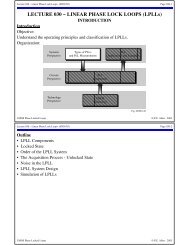
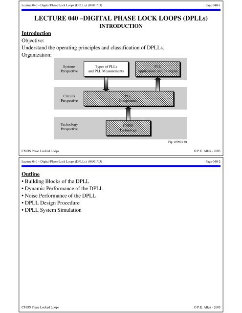
Lecture <strong>040</strong> – Digital Phase Lock Loops (<strong>DPLLs</strong>) (09/01/03) Page <strong>040</strong>-1<strong>LECTURE</strong> <strong>040</strong> –DIGITAL <strong>PHASE</strong> <strong>LOCK</strong> <strong>LOOPS</strong> (<strong>DPLLs</strong>)INTRODUCTIONIntroductionObjective:Understand the operating principles and classification of <strong>DPLLs</strong>.Organization:SystemsPerspectiveCircuitsPerspectiveTypes of PLLsand PLL Measurements;;;;;PLLApplications and Examples;;;;;;;;;;;;;;PLLComponents;;;;;;;;;TechnologyPerspectiveCMOS;;;;;Technology;;;;;Fig. 030901-01CMOS Phase Locked Loops © P.E. Allen - 2003Lecture <strong>040</strong> – Digital Phase Lock Loops (<strong>DPLLs</strong>) (09/01/03) Page <strong>040</strong>-2Outline• Building Blocks of the DPLL• Dynamic Performance of the DPLL• Noise Performance of the DPLL• DPLL Design Procedure• DPLL System SimulationCMOS Phase Locked Loops © P.E. Allen - 2003
V OLFig. 2.2-02Lecture <strong>040</strong> – Digital Phase Lock Loops (<strong>DPLLs</strong>) (09/01/03) Page <strong>040</strong>-3BUILDING B<strong>LOCK</strong>S OF THE DPLLBlock Diagram of the DPLLv 1 , ω 1DigitalAnalogv 2 , ω 2v 2 ', ω 2 ' PhaseDetectorLowpassFilterVCOv d v fFig. 2.2-01÷N Counter(Optional)• The only digital block is the phase detector and the remaining blocks are similar to theLPLL• The divide by N counter is used in frequency synthesizer applications.ω 2 ’ = ω 1 = ω 2N → ω 2 = N ω 1CMOS Phase Locked Loops © P.E. Allen - 2003Lecture <strong>040</strong> – Digital Phase Lock Loops (<strong>DPLLs</strong>) (09/01/03) Page <strong>040</strong>-4DIGITAL <strong>PHASE</strong> DETECTORSIntroductionKey assumption in digital phase detectors: v 1 (t) and v 2 (t) are square waves. This mayrequire amplification and limiting.v in (t)V IHV ILtv outV OHV ILV IHV OLv inV OHv in (t)tTypes of digital phase detectors:1.) EXOR gate2.) The edge-triggered JK flip-flop3.) The phase-frequency detectorCMOS Phase Locked Loops © P.E. Allen - 2003
Lecture <strong>040</strong> – Digital Phase Lock Loops (<strong>DPLLs</strong>) (09/01/03) Page <strong>040</strong>-5The EXOR Gatev 1v 2 'Zero Phase Error:v dG 1Fig. 2.2-03v 1 v 2 ’ v d0 0 00 1 11 0 11 1 0v 1v 2 'v dPositive Phase Error:v 1v 2 'θ e >0v dttv dt Fig. 2.2-04ttv dt Fig. 2.2-05CMOS Phase Locked Loops © P.E. Allen - 2003Lecture <strong>040</strong> – Digital Phase Lock Loops (<strong>DPLLs</strong>) (09/01/03) Page <strong>040</strong>-6EXOR Gate – ContinuedAssume that the average value of v d , is shifted to zero for zero phase error, θ e . v d can beplotted as,V OHv d-ππ2-π2πθ eK d = V OH-V OLπV OLFig. 2.2-06If v 1 and v 2 ’ are asymmetrical (have different duty cycles), then v d becomes,v 1v 2 'v dttv dtV OHv dV OLFig. 2.2-07The effect of waveform asymmetry is to reduce the loop gain of the DPLL and also resultsin a smaller lock range, pull-in range, etc.-ππ2-π2πθ eCMOS Phase Locked Loops © P.E. Allen - 2003
Lecture <strong>040</strong> – Digital Phase Lock Loops (<strong>DPLLs</strong>) (09/01/03) Page <strong>040</strong>-9The Phase-Frequency Detector (PFD)The PFD can detect both the phase and frequency difference between v 1 and v 2 ’.Conceptual diagram:PD LPF 1V LPF1V inω inV outω outPhase FeedbackVCOFrequency FeedbackFD LPF 2V LPF2The output signal of the PFD depends on the phase error in the locked state and on thefrequency error in the unlocked state.Consequently, the PFD will lock under any condition, irrespective of the type of loop filterused.CMOS Phase Locked Loops © P.E. Allen - 2003Lecture <strong>040</strong> – Digital Phase Lock Loops (<strong>DPLLs</strong>) (09/01/03) Page <strong>040</strong>-10The PFD – ContinuedPFD implementation:V DDv 1v 2 'DFF AClk RD RFFClk BQQNo AND Gate With AND GateQ AUpQ B DnFig. 2.2-12Q A Q B Q A Q B0 0 1 0→State=+11 0 0 0→State = 00 1 0 1→State=-11 1PFD State Diagram:State II B State 0 A State IBQ A = 0Q B = 1Q A = 0Q B = 0Q A = 1Q B = 0AA B Fig. 2.2-13Unlike the EXOR gates and the R-S latches, the PFD generates two outputs which arenot complementary.CMOS Phase Locked Loops © P.E. Allen - 2003
Lecture <strong>040</strong> – Digital Phase Lock Loops (<strong>DPLLs</strong>) (09/01/03) Page <strong>040</strong>-11Illustration of a PFDPFD (ω A = ω B ):ABQ APFDQ B(Rising edge triggered) Fig. 2.2-14φ A >φ B :Aφ A
Lecture <strong>040</strong> – Digital Phase Lock Loops (<strong>DPLLs</strong>) (09/01/03) Page <strong>040</strong>-17A Charge-Pump PLL – ContinuedY(s)X(s) = V 2(s)V 1 (s) = ?Y(s) = K os V d(s) = K oK ds 2 [X(s) – Y(s)] → Y(s)X(s) =K o K ds 2 + K o K dwhich has poles at ±j K o K d . To avoid instability, a zero mustbe introduced by the resistor in series with C p .∴V d (s) = I2π⎝ ⎜ ⎜ ⎛R+ 1 IsC = p s2πC (sRC p p +1) = K ds (sτ p +1)⎠ ⎟ ⎟ ⎞Y(s) = K os V d (s) = K oK ds 2 (sτ p +1) [X(s) – Y(s)]⎡⎢Y(s) ⎢ ⎣1 + K oK d⎥s 2 (sτ p +1) = K oK d⎦ s 2 (sτ p +1)X(s)Y(s)X(s) = K o K d (sτ p +1)s 2 + K o K d τ p s + K o K dEquating to the standard second-order denominator gives,ω n = K o K d and ζ = ω nτ p⎤⎥2V DDC pCMOS Phase Locked Loops © P.E. Allen - 2003I 1S1I 2V outS 2RFig. 2.2-21Lecture <strong>040</strong> – Digital Phase Lock Loops (<strong>DPLLs</strong>) (09/01/03) Page <strong>040</strong>-18Nonideal Effects of Charge-Pumps1.) Dead zone.A dead zone occurs when Q A or Q B do not reach their full logiclevels. This is due to delay differences in the AND gate and the flipflops.It is easily removed by proper synchronization of the delays.DeadZonev dθe2.) Mismatch between I 1 and I 2 .To eliminate the dead zone, Q A and Q B can be simultaneouslyhigh for a small time. If I 1 ≠ I 2 , the output varies even though θ e = 0.(Can introduce spurs.)3.) Charge injection.When the S 1 and S 2 switches turn off, they can inject/removecharge from C p . Changes ω 2 .4.) Charge sharing.If X → V DD and Y = 0 when S 1 and S 2 are off, the VCO willexperience a jump when S 1 or S 2 turns on. This periodic effectintroduces sidebands (spurs) at the output.ABQ AQ Bv dV DDFig. 2.2-22tFig. 2.2-23IC 1 xXS 1 v dC y S 2Y C pI 2Fig. 2.2-24CMOS Phase Locked Loops © P.E. Allen - 2003
Lecture <strong>040</strong> – Digital Phase Lock Loops (<strong>DPLLs</strong>) (09/01/03) Page <strong>040</strong>-19DYNAMIC PERFORMANCE OF THE DPLLTypes of PLLsType I – Open-loop transfer function has one pole at the origin.Type II – Open-loop transfer function has two poles at the origin.The above transfer functions may also have other roots but not at the origin.Model for the DPLLθ 1 (s)θ 2 '(s)PDK dLPFF(s)VCOK osθ 2 (s)÷ N CounterOptionalVarious configurations of the DPLL:1.) Phase detector – EXOR, J-K flip-flop, or PFD2.) Filter –Passive lag with or without a charge pumpActive lag with or without a charge pumpActive PI with or without a charge pump1NFig. 2.2-25CMOS Phase Locked Loops © P.E. Allen - 2003Lecture <strong>040</strong> – Digital Phase Lock Loops (<strong>DPLLs</strong>) (09/01/03) Page <strong>040</strong>-20Loop Filters1.) Passive lag-PD → F(s) =1 + sτ 21 + s(τ 1 + τ 2 )PFD → F(s) ≈ 1 + sτ 2s(τ 1 + τ 2 )Experimental results using the PFD with a passive lag filter show that the gain of thepassive filter is not constant. As a result, the filter dynamics become nonlinear.2.) Active lag-1 + sτ 2PD → F(s) = K a 1 + sτ 1PFD → F(s) ≈ 1 + sτ 2sτ 13.) Active PI-PD or PFD → F(s) = 1 + sτ 2sτ 1CMOS Phase Locked Loops © P.E. Allen - 2003
Lecture <strong>040</strong> – Digital Phase Lock Loops (<strong>DPLLs</strong>) (09/01/03) Page <strong>040</strong>-21The Hold Range, ∆ω HThe hold range, ∆ω H , is the frequency range within which the PLL operation isstatically stable. The hold range for various types of <strong>DPLLs</strong> are:Type of PD EXOR EXOR EXOR JK-FF JK-FF JK-FF PFDLoop Filter PassiveLagActiveLagActivePIPassiveLagActiveLagActivePIAllFilters∆ω HK o K d (π/2) oK d (π/2) ∞ K o K d π K o K d K a πN NN N∞ ∞CMOS Phase Locked Loops © P.E. Allen - 2003Lecture <strong>040</strong> – Digital Phase Lock Loops (<strong>DPLLs</strong>) (09/01/03) Page <strong>040</strong>-22The Lock Range, ∆ω LThe lock range is the offset between ω 1 and ω 2 /N that causes the DPLL to acquire lockwith one beat note between ω 1 and ω 2 ’ = ω 2 /N.1.) PD = EXOR v d0.5K d πtRecall that ∆ω L (LPLL) = 2ζω nand ∆ω L ∝ Range of θ e = ∆θ e-0.5K d πω 2 'But, ∆θ e (EXOR)=0.5π ∆θ e (LPLL)2π/∆ω∴ ∆ω L = 0.5π(2ζω n ) = πζω nω 1v dK d πω o∆ω∆ω L = πζω n2.) PD =JK-Flip flop ∆θ e (EXOR) = π ∆θ e (LPLL)t∴ ∆ω L = π(2ζω n )-K d πω 2 'ω 12π/∆ωω o∆ω L = 2πζω n3.) PD = PFD∆θ e (PFD) = 2π ∆θ e (LPLL)→Fig. 2.2-27∆ω L = 2π(2ζω n ) → ∆ω L = 4πζω nThe lock time for all cases is T p ≈ 2π/ω n .ω 2 '(t)ω 2 '(t)tFig. 2.2-26∆ωCMOS Phase Locked Loops © P.E. Allen - 2003t
Lecture <strong>040</strong> – Digital Phase Lock Loops (<strong>DPLLs</strong>) (09/01/03) Page <strong>040</strong>-23The Pull-In Range, ∆ω p , and the Pull-In Time, T pThe pull-in range, ∆ω p , is the largest ∆ω = |ω 1 −ω 2 ’| for which an unlocked loop will lock.The pull-in time, T p , is the time required for the loop to lock.EXOR as the PD:Waveformsvd0.5K d π-0.5K d πT 1 T 2T = 2π/∆ωttFig. 2.2-28CMOS Phase Locked Loops © P.E. Allen - 2003ω 2 '∆ω(t)ω oT = 2π/∆ωT 1 > T 2 because ∆ω is smaller when v d is positive and larger when v d is negative.Results-Type of Filter ∆ω p (Low loop gains) ∆ω p (High loop gains) Pull-in Time, T pPassive Lagπ2 2ζω πnK o K d - ω 2 n2 ζω nK o K4 o 2dπ 2 ζω 3 nActive Lag π2 2ζω n K o K d - ω n 2 πK a2 ζω nK o K4 o 2dπ 2 ζω 3 nActive PI ∞ ∞ 4 o 2π 2 ζω 3 nω 1ω 2 'Lecture <strong>040</strong> – Digital Phase Lock Loops (<strong>DPLLs</strong>) (09/01/03) Page <strong>040</strong>-24The Pull-In Range, ∆ω p , and the Pull-In Time, T p -ContinuedJK Flip-Flop as the PD:WaveformsvdK d π-K d πT 1 T 2T = 2π/∆ωtω 2 'ω o∆ω(t)T = 2π/∆ωω 1ω 2 'tFig. 2.2-29T 1 > T 2 because ∆ω is smaller when v d is positive and larger when v d is negative.Results-Type of Filter ∆ω p (Low loop gains) ∆ω p (High loop gains) Pull-in Time, T pPassive Lag π 2ζω n K o K d - ω 2 n π 2 ζω n K o K d 1 o 2π 2 ζω 2 nActive Lagπ 2ζω n K o K d - ω n 2 π 2 ζω n K o K d 1 ∆ω o 2K a π 2 ζω 2 nActive PI ∞ ∞ 4 ∆ω o 2π 2 ζω 2 nCMOS Phase Locked Loops © P.E. Allen - 2003
Lecture <strong>040</strong> – Digital Phase Lock Loops (<strong>DPLLs</strong>) (09/01/03) Page <strong>040</strong>-25∆ω p and T p for the PFDAssume that the PFD uses a single power supply of V DD . The various waveforms are,v 1V DD0.5V DDv 2 'v d0 tv d (eq.)V DDv dHighImpedanceState0.5V DD(If the filter time constant >> the duty cycle, this waveform simplifies the analysis.)0 tv fV DD0.5V DDω 1∆ωKov d (eq.) is a 50% duty cycle model of the PFD to find T p .T PtFig. 2.2-30CMOS Phase Locked Loops © P.E. Allen - 2003Lecture <strong>040</strong> – Digital Phase Lock Loops (<strong>DPLLs</strong>) (09/01/03) Page <strong>040</strong>-26∆ω p and T p for the PFD – ContinuedSince ∆ω p = ∞, let us find T p using the following model for the passive lag filter:+V R DD1 +R 2v2d C-PFDFilter100% Duty Cycle+v f-V DD2PFD+v d-R 1 +R 22CFilter+v f-50% Duty Cycle Fig. 2.2-31Use the 50% duty cycle model, solve for the time necessary to increase v f by ∆ω/K o .1.) Loop filter = Passive lag⎛ K⎜ o V DD /2 ⎞⎟T p = 2(τ 1 +τ 2 ) ln⎜⎟⎝K o V DD /2 - ∆ω o ⎠2.) Loop filter = Active lag⎛ K⎜ o K a V DD /2 ⎞⎟T p = 2τ 1 ln⎜⎟⎝K o K a V DD /2 - ∆ω o ⎠3.) Loop filter = Active PIT p = 2τ 1∆ω oK o V DD /2For split power supplies, replace V DD with (V OH -V OL ).CMOS Phase Locked Loops © P.E. Allen - 2003
Lecture <strong>040</strong> – Digital Phase Lock Loops (<strong>DPLLs</strong>) (09/01/03) Page <strong>040</strong>-27The Pull-Out Range, ∆ω poThe pull-out range is the size of the frequency step applied to the reference input thatcauses the PLL to lose phase tracking.1.) EXOR: ∆ω po ≈ 2.46ω n (ζ + 0.65) for 0.1 < ζ < 32.) JK Flip-flop:∆ω po = πω n exp ⎢ ⎢⎡ ζ⎣ 1-ζ 2 tan-1 ⎜⎛ 1-ζ 2⎝ ζ ⎠ ⎟⎞⎦ ⎥⎥⎤ , ζ < 1∆ω po = πω n e, ζ = 1∆ω po ≈ 5.78ω n (ζ + 0.5) for all ζ∆ω po = πω n exp ⎢ ⎢⎡ ζ⎣ 1-ζ 2 tanh-1 ⎜⎛ 1-ζ 2⎝ ζ ⎠ ⎟⎞⎦ ⎥⎥⎤ ,ζ > 13.) PFD:∆ω po = 2πω n exp ⎢ ⎢⎡ ζ⎣ 1-ζ 2 tan-1 ⎜⎛ 1-ζ 2⎝ ζ ⎠ ⎟⎞⎦ ⎥⎥⎤ , ζ < 1∆ω po = 2πω n e, ζ = 1∆ω po = 2πω n exp ⎢ ⎢⎡ ζ⎣ 1-ζ 2 tanh-1 ⎜⎛ 1-ζ 2⎝ ζ ⎠ ⎟⎞⎦ ⎥⎥⎤ , ζ > 1∆ω po ≈ 11.55ω n (ζ + 0.5) for all ζCMOS Phase Locked Loops © P.E. Allen - 2003Lecture <strong>040</strong> – Digital Phase Lock Loops (<strong>DPLLs</strong>) (09/01/03) Page <strong>040</strong>-28Example 1 – A Simple CMOS PLLRConsider the PLL shown. Assume that: 1.) the phase2 Cdetector is a simple CMOS EXOR whose logic levels θ in REXOR 1 θ-outVCOare ground and V DD = 5V, 2.) both the input to the PD+loop and the VCO output are square waves thatV DDswing between ground andV DD , and 3.) that the VCO2 Part (d.)has a perfectly linear relationship between the control÷NSU03E1P2voltage and output frequency of 10 MHz/V. Thepolarities are such that an increase in control voltage causes an increase in the VCOfrequency.(a.) Derive the expression for the open-loop transmission and the transfer functionθ out (s)/θ in (s).(b.) Initially assume R 2 = 0 and R 1 = 10kΩ. What value of C gives a loop crossoverfrequency of 100kHz? What is the phase margin. Assume the op amp is ideal.(c.) With the value of C from part (b.), what value of R 2 will provide a phase margin of 45°while preserving a 100 kHz crossover frequency.(d.) Now assume that a frequency divider of factor N is inserted into the feedback path.With the component values of part (c.), what is the largest value of N that can be toleratedwithout shrinking the phase margin below 14°?CMOS Phase Locked Loops © P.E. Allen - 2003
Lecture <strong>040</strong> – Digital Phase Lock Loops (<strong>DPLLs</strong>) (09/01/03) Page <strong>040</strong>-29Example 1 - ContinuedSolution(a.) θ out (s) = K o⎛⎜⎟s F(s)K d ⎜⎟⎝θ in (s) + θ out(s)⎞N = 5K osπ F(s) ⎜ ⎜ ⎛θ⎝ in (s) + θ out(s)N⎠K d = 5V π and F(s) = - R 2+(1/sC)sR 1 C = - sR 2C+1sR 1 C = - sτ 2+1sτ 1, τ 1 = R 1 C and τ 2 = R 2 C∴ θ out (s) = - 5K osπ ⎜ ⎜ ⎛ sτ 2 +1⎝ ⎠ ⎟ ⎟ ⎞ ⎛⎜⎟sτ⎜ 1θ ⎟⎝ in (s) + θ out(s) ⎞N ⎠⎡⎢θ out (s) ⎢ 1 + 5K o⎛sτ ⎜ 2 +1⎞⎣sπN ⎜ ⎝sτ 1= 5K o⎛sτ ⎜ 2 +1⎞⎟sπ ⎜ ⎟ ⎝sτ 1θ in (s)θ out (s)θ in (s) =θ out (s)θ in (s) =⎤⎟⎥⎟⎥⎠⎦- 5K oπτ 1(sτ 2 +1)s 2 + 5K oπN τ 2τ 1s + 5K oπNτ 1- 5K oπτ 1(sτ 2 +1)s2+ 5K o τ 2πN τ 1s + 5K and the loop gain = LG = - 5K o⎜osNπ ⎜ ⎝πNτ 1Assume N = 1 to get the answer to part (a.).⎠CMOS Phase Locked Loops © P.E. Allen - 2003⎛⎠ ⎟ ⎟ ⎞sτ 2 +1⎞sτ 1⎟⎟⎠Lecture <strong>040</strong> – Digital Phase Lock Loops (<strong>DPLLs</strong>) (09/01/03) Page <strong>040</strong>-30Example 1 - Continued(b.) With R 2 = 0, τ 2 = 0 so that the loop gain becomes,5K oLG = - s 2 τ 1 Nπ = 5·2πx107s 2 τ 1 π = 10 8108ω c2τ = 1 → τ 1 1 = (2π·10 5 ) 2 = 253.3µsec.τ 1 = R 1 C → 253.3µsec. = 10kΩC → C = 25.3nFThe phase margin is 0°.(c.) The phase margin is totally due to τ 2 . It is written as,PM = tan -1 (ω c τ 2 ) = 45° → ω c τ 2 = 1 → τ 2 = 1 1ω c= 2πx10 5 = 1.5915µs = R 2 C1∴ R 2 = 2πx10525.3x10-9 = 62.83Ω(d.) N does not influence the phase shift so we can write,tan -1 (ω c τ 2 ) = 14° → ω c ’τ 2 = 0.2493 → ω c ’ = 0.2493ω c = 156,657 rads/sec.Now the loop gain at ω c ’ must be unity.LG = -N =5K oω c ’Nπ⎝ ⎜⎛(ω c ’τ 2 ) 2 +1ω ⎠ ⎟⎞5K oc ’τ 1= 1 → N = (ω c ’)2πτ 1(ω c ’τ 2 ) 2 +110 8(156,657) 2 253.3x10 -6 (0.2493) 2 +1 = 16.58 = 16CMOS Phase Locked Loops © P.E. Allen - 2003
Lecture <strong>040</strong> – Digital Phase Lock Loops (<strong>DPLLs</strong>) (09/01/03) Page <strong>040</strong>-31NOISE PERFORMANCE OF THE DPLLCombination of Noise and InformationIn the LPLL, the noise and information signals are added because of the linearmultiplier PD.The noise supression of DPLL’s is generally better than LPLL’s but no theory of noiseexists for the DPLL.The following pages provide some insight into the noise performance of the DPLL.CMOS Phase Locked Loops © P.E. Allen - 2003Lecture <strong>040</strong> – Digital Phase Lock Loops (<strong>DPLLs</strong>) (09/01/03) Page <strong>040</strong>-32Noise Performance of a DPLL with an EXOR PDθ jv 1v 2 'v dPhase noise ata given inbandfrequencytInput withphase noisesuperimposed(phase jitter)v 1jθ j θ j θ jIdeal Inputθ j θ j θ jDetectorOuputv d100%50%0%v d is proportionalto the phase noise.∴ LPLL noise theory≈ DPLL noise theory.tFig. 2.2-32CMOS Phase Locked Loops © P.E. Allen - 2003
Lecture <strong>040</strong> – Digital Phase Lock Loops (<strong>DPLLs</strong>) (09/01/03) Page <strong>040</strong>-33Phase Noise in a Communication SignalConsider the following simple noise model-Noiseless binary information signal:v 1Above signal after transmission through a bandlimited system:v 1btSuperposition of noise:v 1nReshaped signal:v;;1r;;;;PhaseJitter;; ;;;;;; ;;;;V upperV lowerCMOS Phase Locked Loops © P.E. Allen - 2003tttFig. 2.2-33Lecture <strong>040</strong> – Digital Phase Lock Loops (<strong>DPLLs</strong>) (09/01/03) Page <strong>040</strong>-34Input Signal-to-Noise RatioThe input signal noise ratio of a pulse with phase jitter is defined as,1SNR i =2 θ 2 n1whereθ 2 n1 ≈ W236where,v 1WtCMOS Phase Locked Loops © P.E. Allen - 2003
Lecture <strong>040</strong> – Digital Phase Lock Loops (<strong>DPLLs</strong>) (09/01/03) Page <strong>040</strong>-35Phase Noise in a DPLL with a JK Flip-Flop and a PFDThe basic difference is that the JK Flip-flop and PFD are edge-triggered.When the input signal fades (v 1 →0), the reshaped signal can stick at a distinct logiclevel.Conclusion:The noise suppression of the DPLL is about the same for all phase detectors as long asnone of the edges of the reference get lost by fading. If fading occurs, the EXOR offersbetter noise performance.Summary of DPLL Noise Performance:P s = input signal powerP n = input noise powerB i = input noise bandwidthB L = noise bandwidth ≈ ω n2 ⎝ ⎜ ⎛ζ + 1 4ζ⎞⎟⎠SNR i = SNR of the input signal = P sP nSNR L = SNR of the loop = SNR iB i2B LCMOS Phase Locked Loops © P.E. Allen - 2003Lecture <strong>040</strong> – Digital Phase Lock Loops (<strong>DPLLs</strong>) (09/01/03) Page <strong>040</strong>-36DPLL DESIGN PROCEDUREDesign ProcedureObjective: Design K o , K d , ζ, and F(s)Given: Phase detector and VCOSteps:1.) Specify f 1 (min), f 1 (max), f 2 (min), and f 2 (max).2.) Design N unless otherwise specified.Given: ω n (min) < ω n < ω n (max) and ζ min < ζ < ζ maxFor these ranges we get approximately,ω n (max)ω n (min) =N maxN minandζ maxζ min=N maxN min→ N = N mean = N max N min3.) Determine ζ. Typically, ζ ≈ 0.7.4.) If noise is of concern, continue with the next step, otherwise go to step 12.5.) If there are missing edges in the input signal (fading), go to step 6, otherwise go tostep 7.6.) Choose an EXOR phase detector. Continue with step 8.K d = V OH-V OLπCMOS Phase Locked Loops © P.E. Allen - 2003
Lecture <strong>040</strong> – Digital Phase Lock Loops (<strong>DPLLs</strong>) (09/01/03) Page <strong>040</strong>-37Design Procedure – Continued7.) Choose the JK Flip-flop or PFD as the phase detector.K d = V OH-V OL2π (JK flip-flop)K d = V OH-V OL4π (PFD)8.) Specify B L .B L should be chosen so that SNR i B i2B L≥ 4θ n12 → SNR i and B i ⇒ B L• If N changes, this can create a problem becauseB L = ω n ⎛ ⎞⎜2 ζ + 1 ⎟⎝ 4ζ ⎠and both ω n and ζ vary with N.• Need to check that B L (min) is large enough.• If B L is too small, then N should be increased.CMOS Phase Locked Loops © P.E. Allen - 2003Lecture <strong>040</strong> – Digital Phase Lock Loops (<strong>DPLLs</strong>) (09/01/03) Page <strong>040</strong>-38Design Procedure – Continued9.) Find K o .K o = ω 2(max)-ω 2 (min)v f (max)-v f (min)10.) Find ω n given B L and ζ.ω n = 8B Lζ1+4ζIf N is variable, use B L and ζ correspondingly to N = N mean .11.) Specify the loop filter.Given ω n , ζ, K o , K d , and N find τ 1 , τ 2 , and K a (K a >1).Go to step 19.12.) Continued from step 4.Choose the PFD →13.) Find K o .K o = ω 2(max)-ω 2 (min)v f (max)-v f (min)K d = V OH-V OL4πCMOS Phase Locked Loops © P.E. Allen - 2003
Lecture <strong>040</strong> – Digital Phase Lock Loops (<strong>DPLLs</strong>) (09/01/03) Page <strong>040</strong>-39Design Procedure – Continued14.) Specify the type of loop filter. Use the passive lag filter as the others offer nobenefits.15.) Determine ω n .a.) Fast switching (T p ). Go to step 16.b.) DPLL does not lock out when switching from N o f ref to (N o +1) f ref . ∴ ∆ω po
Lecture <strong>040</strong> – Digital Phase Lock Loops (<strong>DPLLs</strong>) (09/01/03) Page <strong>040</strong>-41Flowchart of the DPLL Design ProcedureYesUse EXORYesAre there missing edges?Specify the noise bandwidth, B LDesign the VCOSpecify the range of f 1 and f 2Determine N or range of NDetermine ζ or range of ζNoIs Noise Suppression Required?NoChoose the PFD, design the VCO and the loop filterUse PFDTP Given T P , ∆ω po , or T L∆ω T po LUse T P to find τ 1 or τ 1 +τ 2Use ∆ω po and ζ to find ω n Use T L to find ω nEstimate ω n from τ 1Use ω n and ζ to find τ 1Use B L and ζ to find ω nSelect the loop filter and determine τ 1 , τ 2 , (K a )Use ω n and ζ to find τ 2Calculate the loop filter values Fig. 2.2-37CMOS Phase Locked Loops © P.E. Allen - 2003Lecture <strong>040</strong> – Digital Phase Lock Loops (<strong>DPLLs</strong>) (09/01/03) Page <strong>040</strong>-42Design Example – A Frequency Synthesizer Using the 74HC/HCT4076Design a DPLL frequency synthesizer using the CMOS 74HC/HCT4076 PLL. Thefrequency sythesizer should be able to produce a set of frequencies in the range of 1MHzto 2MHz with a channel spacing of 10kHz. Use a PFD and a passive lag-lead filter.Design:1.) Determine the ranges of the input and output frequencies.f 1 is constant at 10kHz. f 2 (min) = 1MHz and f 2 (max) = 2MHz2.) Choose N.N max = 2MHz10kHz = 200 and N min = 1MHz10kHz = 100∴ N mean = N max·N min = 1413.) Find ζ. Start by choosing ζ = 0.7 and find ζ max and ζ min .ζ maxζ max=N maxN min= 2 and ζ = ζ max·ζ min = 0.7∴ ζ 2 min 2 =0.49 → ζ min = 0.59 and ζ max = 0.59 2 = 0.83∴ 0.59 < ζ < 0.83 which is consistent with our choice of ζ.4.) Select the PFD as the phase detector. For the 74HC/HCT4076, V OH = 5V andV OL =0V. This gives a K d = 5V/4π = 0.4 V/rad.CMOS Phase Locked Loops © P.E. Allen - 2003
Lecture <strong>040</strong> – Digital Phase Lock Loops (<strong>DPLLs</strong>) (09/01/03) Page <strong>040</strong>-43Design Example – Continued5.) According to the data sheet of thef 2 (MHz)74HC4046A, the VCO operates linearly in thevoltage range of v f = 1.1V to 3.9V as shown.2∴ K o = 2x106 x2π3.9-1.1 = 2.2x10⁶ rads/V·sec 1The data sheet also requires calculation of1.1V3.9Vtwo resistors, R 1 and R 2 , and a capacitor, C 1 .Using the graphs from the data sheet gives,R 1 = 47kΩ, R 2 = 130kΩ, and C 1 = 100pF.6.) Assume the loop should lock with 1ms.0 1 2 3 4 5∴ T L = 1ms → ω n = 2π/T L = 6280 rads/sec.7.) Using a passive loop filter we get,τ 1 +τ 2 = K oK dNω 2 = 2.2x106·0.4n 141·6280 2 = 161µs8.) τ 2 = 2ζω n= 2·0.76280 = 223µs !!! (The problem is that τ 1+τ 2 is too small)Go back and choose T L = 2ms → ω n = 2π/T L = 3140 rads/sec.τ 1 +τ 2 = K oK dNω 2 = 2.2x106·0.4n 141·3140 2 = 633µs and τ 2 = 2ζω n= 2·0.73140 = 446µs → τ 1 = 187µsv f (V)Fig. 2.2-35CMOS Phase Locked Loops © P.E. Allen - 2003Lecture <strong>040</strong> – Digital Phase Lock Loops (<strong>DPLLs</strong>) (09/01/03) Page <strong>040</strong>-44Design Problem – Continued9.) Design the loop filter.For optimum sideband supression, C should be large. Choose C = 0.33µF.∴ R 1 = τ 1C = 187x10-60.33x10 -6 = 567Ω and R 2 = τ 2C = 446x10-60.33x10 -6 = 1.351ΩThe data sheet requires that R 1 +R 2 ≥ 470Ω which is satisfied.Block diagram of the DPLL frequency synthesizer design of this example:C 1 =100pFv 1 (10kHz) SIGinCOMPinv 2 'PC1(EXOR)74HC4046AC1AC1BData NP0····P7PEPC2(PFD)PCP outVCOVCOoutCP74HC40102(40103)TCv 2 'PC3(JK)TE PL MRPC2 out VCOin R1 R2R 1 =R 1 =567Ω47kΩR 2 =1.35kΩR 2 =130kΩ+5VC = 0.33µFFig. 2.2-36CMOS Phase Locked Loops © P.E. Allen - 2003
Lecture <strong>040</strong> – Digital Phase Lock Loops (<strong>DPLLs</strong>) (09/01/03) Page <strong>040</strong>-45Simulation of the DPLL ExampleThe block diagram of this example is shown below.θ 1 (s)θ 2 '(s)PDK dLPFF(s)VCOK osθ 2 (s)÷ N CounterOptionalThe PFD-charge pump combination can be approximated as †K d (1+sτ 2 )“K d F(s)” = s(τ 1 +τ 2 )Therefore, the loop gain becamesLG(s) = K oK d (1+sτ 2 )s 2 (τ 1 +τ 2 )=K v (1+sτ 2 )(s+ε) 2 (τ 1 +τ 2 )1NFig. 2.2-25(the factor ε is used for simulation purposes)For this problem,K d = 0.4V/rad., K o = 2.2x10 6 , τ 2 = 446µs, and τ 2 +τ 2 = 633µs. Also choose ε = 0.01.† R.E. Best, “Phase-Locked Loops – Design, Simulation, and Applications,” 4 th Ed., McGraw-Hill, NY, p. 103CMOS Phase Locked Loops © P.E. Allen - 2003Lecture <strong>040</strong> – Digital Phase Lock Loops (<strong>DPLLs</strong>) (09/01/03) Page <strong>040</strong>-46Simulation of the DPLL Example – ContinuedPSPICE Input FileDPLL Design Problem-Open Loop Response - BestVS 1 0 AC 1.0R1 1 0 10K* Loop bandwidth = Kv =8.8x10E5 sec.-1 Tau1=187E-6 Tau2=446E-6 N=141ELPLL 2 0 LAPLACE {V(1)}= {8.8E+6/(S+0.01)/141*(0.446E-3*S+1)/(S+0.01)/0.633E-3}R2 2 0 10K*Steady state AC analysis.AC DEC 20 10 100K.PRINT AC VDB(2) VP(2).PROBE.END100Simulation Results:80Note that the phase is veryclose to 0° and |LG|>>1 atlow frequencies which istypical of type II systems.dB or Degrees6<strong>040</strong>LG Phase20Phase|LG|0Margin≈ 84°-20ω c-4010 100 1000 10 4 10 5Frequency (Hz)CMOS Phase Locked Loops © P.E. Allen - 2003
Lecture <strong>040</strong> – Digital Phase Lock Loops (<strong>DPLLs</strong>) (09/01/03) Page <strong>040</strong>-47DPLL SYSTEM SIMULATIONExamples of Case Studies using the Best Software †PLL Parameters-Supply voltages:Positive supply = 5V Negative supply = -5VPhase detector:V + sat = 4.5V V - sat = 0.5VLoop filter:τ 1 = 500µs τ 2 = 50µsOscillator:K o = 130,000 rads/V·sec V + sat = 4.5V V - sat = 0.5VThe simulation program will be used to verify the following calculated values:ω n = 17,347 rads/sec.ζ = 0.486∆f po = 7719 Hz∆f p = 13,192 Hz† Roland E. Best, Phase-Locked Loops – Design, Simulation, and Applications, 4 th ed., McGraw-Hill Book Co., 1999, New York, NYCMOS Phase Locked Loops © P.E. Allen - 2003Lecture <strong>040</strong> – Digital Phase Lock Loops (<strong>DPLLs</strong>) (09/01/03) Page <strong>040</strong>-48Case 1 – System Benchmarkv dv d (mV)v ft(µs)CMOS Phase Locked Loops © P.E. Allen - 2003
Lecture <strong>040</strong> – Digital Phase Lock Loops (<strong>DPLLs</strong>) (09/01/03) Page <strong>040</strong>-49Case 2 - ∆f = 8000Hzv dv d (V)↑Phase error≥ 90°v fCMOS Phase Locked Loops © P.E. Allen - 2003Lecture <strong>040</strong> – Digital Phase Lock Loops (<strong>DPLLs</strong>) (09/01/03) Page <strong>040</strong>-50Case 3 – Loop Just Locks Outv fvfv d (V)vdv d← Loop pulls outCMOS Phase Locked Loops © P.E. Allen - 2003
Lecture <strong>040</strong> – Digital Phase Lock Loops (<strong>DPLLs</strong>) (09/01/03) Page <strong>040</strong>-51Case 4 – Pull-In Range Verification4.5v f4.03.53.0v dv d (V)2.52.01.51.00.5Loop will not pull back in for df > 14,200 HzCMOS Phase Locked Loops © P.E. Allen - 2003Lecture <strong>040</strong> – Digital Phase Lock Loops (<strong>DPLLs</strong>) (09/01/03) Page <strong>040</strong>-52Case 5 – PFD and Illustration of a Virtually Infinite Pull-In Range∆f p = ±40kHz ∆f = 35 kHz to avoid clipping of v f .v d (V) v dv fT p ≈ 1.5msCMOS Phase Locked Loops © P.E. Allen - 2003
Lecture <strong>040</strong> – Digital Phase Lock Loops (<strong>DPLLs</strong>) (09/01/03) Page <strong>040</strong>-53Case 6 – EXOR with Active PI Filter4.54.03.5v fv d (V)3.02.52.01.51.00.5v dT p ≈ 5msCMOS Phase Locked Loops © P.E. Allen - 2003Lecture <strong>040</strong> – Digital Phase Lock Loops (<strong>DPLLs</strong>) (09/01/03) Page <strong>040</strong>-54SUMMARY• The DPLL has a digital phase detector and the remainder of the blocks are analog• Digital phase detectors- EXOR Gate- JK Flip-Flop- Phase-Frequency Detector• Charge pump – a filter implementation using currents sources and a capacitor thatworks with the PFD• Charge pumps implement a pole at the origin to result in zero phase error• The DPLL is much more compatible with IC technology and is the primary form of PLLused for frequency synthesizersCMOS Phase Locked Loops © P.E. Allen - 2003