EE-461 Lab #3 Digital Communications Systems - Capitol College ...
EE-461 Lab #3 Digital Communications Systems - Capitol College ...
EE-461 Lab #3 Digital Communications Systems - Capitol College ...
You also want an ePaper? Increase the reach of your titles
YUMPU automatically turns print PDFs into web optimized ePapers that Google loves.
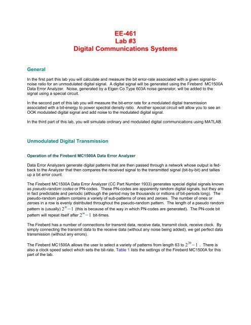
Noise Inn(t)Test PointSignal Ins(t)+r(t)+–DetectedSignal Out2.5 voltsFigure 1. Block diagram of circuit to add signal to noise for “Unmodulated <strong>Digital</strong> Transmission.”Data Error AnalyzerRxCLKTxCLKRxDNoise SourceTxDSignal InNoise InSummerDetectedSignal OutFigure 2. Setup configuration for “Unmodulated <strong>Digital</strong> Transmission.”
Probability of ErrorThe noise generated by the 1350-B has a Gaussian distribution. Let n be the random variable associatedwith the noise signal. The probability distribution for n is given byp n(n )= 1n22σe− 2 ,σ √2πwhere σ is the (RMS) noise voltage (to be measured). When this noise is added to a signal, two types oferrors can occur: the signal is a logical zero and the noise is positive and greater than half-way between thelogical zero voltage and the logical one voltage (2.5 V for TTL); (2) the signal is a logical one and the noiseis negative and less than the half-way point. In either case, given the noise (RMS) voltage, and the half-waypoint, the probability of error is the same:∞P (error)=∫ 2.5by a change of variables, this integral is also equal toP (error )=∫ 2.5σ∞ 1√2πn21 2σe− 2 dn.σ √2πe−z22 dz≡Q ( 2.5σ ).Bit Error Rate Measurements and PredictionsBy cycling the switch, a PN-sequence is generated by the Fireberd. The received sequence is compared tothe transmitted sequence, and the number of bit errors is determined. The length of the test sequence isdetermined by the pattern select.The probability of error should be equal to the bit error rate. The probability of error is determined by thenoise (RMS) voltage (if the threshold is constant). In general, the probability of error is determined by thesignal-to-noise ratio, that is the ratio of the signal power to the noise power:SNR=10 log12 52σ 2 =20log 5σ √2 .Given a signal-to-noise ratio, we may calculate the probability of error (and, hence, predict the bit error rate)by first converting the dB signal-to-noise ratio to linear, dividing by the square root of two, and evaluating theQ-function at this value. To set the signal-to-noise, simply find the sigma corresponding to the given valuefor the dB signal-to-noise ratio, and adjust the noise output to the summer (setting the signal switch off) tohave that σ value.By setting the noise voltage (as indicated above), and calculating the probability of error (indicated in“Probability of Error”), fill-in the following table (Table 2) for probability of error and bit error rate for varioussignal-to-noise levels. Write the result under BER (measured). If the probability of error is not indicated onthe ‘Q’ tables, use an appropriate approximation.
SNR σ Error Probability BER (Measured)20151050Table 2. Bit Error-Rate Measurements for “Unmodulated <strong>Digital</strong> Transmission.”Modulated <strong>Digital</strong> TransmissionMuch higher bit rates for digital transmission may be obtained by digital modulation, that is by transformingdigital signals to sine waves (of various frequencies, amplitudes or phases). In this lab you will use a circuitthat performs an OOK modulation and demodulation of a digital signal. Noise will be added to themodulated signal, and we will predict and measure the effect of this noise (in terms of BER) on thedemodulation (detection) process.OOK Modulation and DemoduationOOK (digital) modulation is the equivalent of amplitude modulation of a sine wave with a unipolar signal (onewhere logic ‘0’ is 0V and logic ‘1’ is some positive value [say 5V]). When the digital input is 0, we have amodulated signal of 0V; when the digital input is 1, we have a modulated signal that is a sine wave.Modulation is performed by multiplication of the digital signal by the sine wave. Demodulation is performedby multiplication of the modulated signal by a sine wave of the same frequency, integrating the product andthreshold detecting the output of the integrator. The threshold is (usually) set halfway between the detectedoutput value for a ‘0’ and the detected value for a ‘1’.The circuit whose block diagram is in Figure 3 performs the digital modulation and demodulation. This circuitalso allows for the addition of noise to the modulated signal. We specifically wish to see what happenswhen noise is integrated. The effect of the integration of noise will ultimately determine the probability oferror in (most) digital modulation/demodulation systems. The circuit corresponding to Figure 3 produces aclock that drives the data error analyzer. This clock is derived from an internal clock that also drives thecounter connected to a ROM whose output goes to a digital-to-analog converter (DAC). The output of thedigital-to-analog converter is a sine wave corresponding to the carrier. This sine wave may be amplitudemodulated if a multiplying digital-to-analog converter is used. Because we have a single clock used togenerate the carrier and the data clock, we may achieve carrier coherency, that is the phasing between thecarrier and the data is fixed.Using the circuit corresponding to Figure 3, set-up the configuration in Figure 4. This configuration uses aData Error Analyzer (Fireberd 1500A) to generate a PN sequence. The PN sequence from the Data ErrorAnalyzer is modulated OOK by a sine wave generated by the circuit, then has noise added to the modulatedsignal, and then the modulated signal with noise is demodulated. When hooking-up this equipment, firstverify that we have perfect error transmission when no noise is added. Use the settings in Table 3 for theData Error Analyzer.
OptionSettingGenerator ClockExternal I/FPattern 63Error InsertOffDataNormTestNormAudioOffAuto SyncDisableBER Mode 10 5RTSOffInput Impedance8 K-Ohms (on back)Modeunipolar unbalanced (on back)Table 3. Settings for the Fireberd Data Error Analyzer for “Modulated <strong>Digital</strong> Transmission.”Addition of Signal to NoiseSet the noise generator bandwidth to 500 kc (this is not the true bandwidth).Probability of ErrorThe received (modulated) signal r (t ) can be decomposed into its (undistorted) signal component s(t ) anda noise component n( t ) :r (t )=s(t )+n(t ).In this lab s(t )=A cosω c t and n( t ) is a noise signal whose bandwidth is W and whose power spectraldensity is N 0(the noise power spectral density is constant over the bandwidth). ( A is the peak value of the2modulated sine wave [without noise] and can be measured from Test Point #2. The power spectral densityN 0may be measured using a spectrum analyzer connected to the output of the Noise Generator.)2Demodulation (detection) is performed by integrating the product of the received signal and B cosω ct .Integrating this product amounts to converting this random signal into a random variable. Let r d be thisrandom variable, that is, the value of the integral of the product.wherer d =∫ 0Tr(t ) B cosωc t dt=s d +n d .s d=∫ 0Ts(t ) B cosωc t dt= AB∫ 0Tcos 2 ω ct dt=AB T 2 ,n d=∫ 0Tn(t ) B cosωc t dt .
The variable r dis a Gaussian random variable with mean μ rd = AB T 2and variance σ 2nd (the variance of r dis the same as the variance of n d). The variance of n dis found as follows:σ 2 nd = E {n 2 T Td } = E {∫ 0 n(t ) B cos ωc t dt∫ 0 n( s) B cos ωc s ds}= B 2 ∫ 0TE {n(t )n( s)} cos ωc t cosω cs dt ds= B 2 T N∫002 δ (t−s) cosω c t cosω c s dt ds= B 2 N 0∫ T2 0 cos 2 ω cts dt= B N 2 0 T4 .(The last is true assuming that ω cis an integral multiple of 2πT .Thus, drawing from the results in Basic <strong>Digital</strong> Transmission in Noise, we have for the probability of error,P (error )=Q( μ rd /2σ nd) =Q ABT /4( B √ N o T /2 ) ( =Q A √ T 2 N 0) .Note that the larger the value for T, the lower the probability of error. (No matter how large the noise powerspectral density is, we can demodulate and detect the signal with arbitrarily low probability of error if weintegrate long enough.)Bit Error Rate Measurements and PredictionsThe circuit corresponding to Figure 3 performs an integrate-and-dump over only half of the digital bit period(for reasons of circuit simplicity). Therefore, in order to corroborate the measured value with the predicted(calculated) value, the value for T must be one-half the bit period. For the case of this circuit, T = 32 over10 6 = 32 µs.By calculating the probability of error and setting the noise voltage (the same way as indicated in Basic<strong>Digital</strong> Transmission in Noise), fill-in Table 4 for probability of error and bit error rate for the various signal-tonoiselevels. The first step in filling in any one line of this table is to first compute N ofrom E bN 0whereE b= A2 T2. (The value A is the peak modulated amplitude, which may be measured from the signal atTest Point # 2.) Given A , T and E bN 0(as a dB value), we may find N o2 :
dB = 10 log E bN 0.dB1010 = E b.N 0N 0 = A2 T2⋅10dB10.The second step is to compute the noise (rms) voltage (to be measured at Test Point #2) from therelationship σ n2=WN 0, where W is the bandwidth of the noise signal. This bandwidth may be determinedby observing the noise on a spectrum analyzer (do not trust the bandwidth setting on the noise generator).σ n2 is the noise variance. The parameter σ n2 is the (rms) noise voltage measured by the True RMSVoltmeter from Test Point #2.Should it be impossible to add enough noise to generate the appropriate E bN 0indicate why.ratio, leave that entry blank andE bN 0N(dB) 0σ n Error Probability BER (Measured)4035302520151050Table 4. Bit Error-Rate Measurements for “Modulated <strong>Digital</strong> Transmission.”
Questions1. What would the true rms voltage of a TTL waveform be? Assume an equal number of zeroes andones2. List the noise voltages and powers corresponding to BER's of 1E-5, 1E-6, 1E-7 and 1E-8 for a TTLwaveform. Find the signal-to-noise ratio in each case. Express the signal-to-noise ratio in dB.3. List the noise voltages and powers corresponding to BER's of 1E-5, 1E-6, 1E-7 and 1E-8 for anOOK modulated waveform. Find the bit-energy-to-power spectral density ratio E bN 0Express the values in dB.in each case.


