

Semiconductor Physics Sectional Programme Overview ...
Semiconductor Physics Sectional Programme Overview ...
Semiconductor Physics Sectional Programme Overview ...

Create successful ePaper yourself
Turn your PDF publications into a flip-book with our unique Google optimized e-Paper software.
<strong>Semiconductor</strong> <strong>Physics</strong> <strong>Sectional</strong> <strong>Programme</strong> <strong>Overview</strong><br />
Prof. Dr. Werner Wegscheider (DPG)<br />
Universität Regensburg<br />
Postfach<br />
93040 Regensburg, Germany<br />
werner.wegscheider@physik.uni-regensburg.de<br />
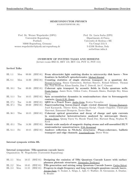
Invited Talks<br />
SEMICONDUCTOR PHYSICS<br />
HALBLEITERPHYSIK (HL)<br />
Prof. Dr. Lucia Sorba (EPS)<br />
Dipartimento di Fisica<br />
Università di Modena e RE<br />
Via Campi 213/A<br />
I-41100 Modena, Italy<br />
sorba@tasc.infm.it<br />
OVERVIEW OF INVITED TALKS AND SESSIONS<br />
(lecture rooms HSZ 01, BEY 118, BEY 154, POT 51, POT 151)<br />
HL 1.1 Mon 09:30 (HSZ 01) From ultraviolet light emitting diodes to microcavity disk lasers - New<br />
frontiers in InAlGaN optoelectronics, Michael Kneissl<br />
HL 8.1 Mon 14:30 (HSZ 01) Counting statistics of single electron transport in a quantum dot,<br />
Renaud Leturcq, Simon Gustavsson, Barbara Simovic, Roland Schleser, Thomas<br />
Ihn, Paul Studerus, Klaus Ensslin, Dan C. Driscoll, Art C. Gossard<br />
HL 10.1 Tue 09:30 (HSZ 01) Coherent spin transport by acoustic fields in GaAs quantum wells,<br />
Paulo Santos, James Stotz, Odilon Couto, Fernando Iikawa, Rudolph Hey, Klaus<br />
Ploog<br />
HL 11.1 Tue 10:15 (HSZ 01) Spin accumulation dynamics in semiconductors close to ferromagnetic<br />
contacts, Gerrit E.W. Bauer<br />
HL 17.1 Tue 14:30 (HSZ 01) QED in a Pencil Trace, Andre Geim, Kostya Novoselov<br />
HL 37.1 Thu 09:30 (HSZ 01) Superconducting boron-doped single crystal diamond, Etienne Bustarret,<br />
Jozef Kacmarcik, Thierry Klein, Benjamin Sacépé, Claude Chapelier, Christophe<br />
Marcenat, Emmanuel Bourgeois, Xavier Blase<br />
HL 38.1 Thu 10:15 (HSZ 01) Coherent optical generation and decay of charge and spin currents<br />
in semiconductor heterostructures analyzed by microscopic theory,<br />
Torsten Meier, Quang Tuyen Vu, Huynh Thanh Duc, Hartmut Haug, Stephan W.<br />
Koch<br />
HL 45.1 Thu 14:30 (HSZ 01) Atomic scale analysis of magnetic doping atoms and self-assembled III/V<br />
semiconductor nanostructures, P.M. Koenraad<br />
HL 51.1 Fri 10:15 (HSZ 01) Andreev reflection in Nb-InAs structures: Phase-coherence, ballistic<br />
transport and edge channels, JonathanEroms, Dieter Weiss<br />
Internal symposia within HL<br />
Internal symposium: THz-quantum cascade lasers<br />
Organization: W. Wegscheider (Universität Regensburg)<br />
HL 2.1 Mon 10:15 (HSZ 01) Designing the emission of THz Quantum Cascade Lasers with surface<br />
plasmon photonic structures, Alessandro Tredicucci<br />
HL 2.2 Mon 10:45 (HSZ 01) THz generation and mixing using Quantum Cascade Lasers, Carlos Sirtori<br />
HL 2.3 Mon 11:15 (HSZ 01) Progress in single frequency and long wavelength quantum cascade lasers,<br />
Jerome Faist, G. Scalari, L. Sirigu, L. Ajili, C. Walther, M. Giovannini, A. Dunbar,<br />
R. Houdre
<strong>Semiconductor</strong> <strong>Physics</strong> <strong>Sectional</strong> <strong>Programme</strong> <strong>Overview</strong><br />
HL 2.4 Mon 11:45 (HSZ 01) Growth and Processing of GaAs quantum cascade lasers, Gottfried Strasser,<br />
Aaron Maxwell Andrews, Tomas Roch, Gernot Fasching, Alexander Benz, Sebastian<br />
Golka, Maximilian Austerer, Christian Pfluegl, Werner Schrenk, Karl Unterrainer<br />
HL 2.5 Mon 12:15 (HSZ 01) GaInAs/AlAsSb quantum cascade lasers: a new approach towards 3-to-<br />
5 µm semiconductor lasers, Joachim Wagner, Quankui Yang, Christian Manz,<br />
Wolfgang Bronner, Christian Mann, Klaus Köhler<br />
Internal symposium: Quantum optics in semiconductors<br />
Organization: M. Bayer (Universität Dortmund)<br />
HL 12.1 Tue 11:15 (HSZ 01) Quantum Light Generation from <strong>Semiconductor</strong> Quantum Dots,<br />
Andrew Shields<br />
HL 12.2 Tue 11:45 (HSZ 01) Size-tunable exchange interaction in InAs/GaAs quantum dots,<br />
U. W. Pohl, A. Schliwa, R. Seguin, S. Rodt, K. Pötschke, D. Bimberg<br />
HL 12.3 Tue 12:15 (HSZ 01) Quantum Optics of Excitons in <strong>Semiconductor</strong>s, Heinrich Stolz<br />
HL 12.4 Tue 12:45 (HSZ 01) Microscopic Theory of <strong>Semiconductor</strong> Quantum Optics, Mackillo Kira,<br />
Stephan W. Koch<br />
HL 18.1 Tue 15:15 (HSZ 01) Light Matter Interaction Effects in Quantum Dot Microcavities, S. Reitzenstein,<br />
C. Hofmann, A. Löffler, J. P. Reithmaier, M. Kamp, A. Forchel, G. Sek,<br />
V. D. Kulakovskii, A. Bazhenov, A. Gorbunov, L. V. Keldysh, T. L. Reinecke<br />
HL 18.2 Tue 15:45 (HSZ 01) CQED with II-VI nanocrystals, Ulrike Woggon, Nicolas LeThomas, Oliver<br />
Schoeps, Mikhail Artemyev<br />
HL 18.3 Tue 16:00 (HSZ 01) Deutsch-Jozsa Algorithm using Triggered Single Photons from a Single<br />
Quantum Dot, Oliver Benson, Matthias Scholz, Thomas Aichele, Sven Ramelow<br />
HL 18.4 Tue 16:30 (HSZ 01) Imaging the Local Density of Photonic States in Photonic Crystal<br />
Nanocavities, Michael Kaniber, Felix Hofbauer, Simon Grimminger, Max Bichler,<br />
Gerhard Abstreiter, Jonathan J. Finley<br />
HL 18.5 Tue 16:45 (HSZ 01) Theory of optical properties for quantum dots in microcavities,<br />
Frank Jahnke, Jan Wiersig, Norman Baer, Christopher Gies<br />
Internal symposium: New phenomena in edge transport of QHE systems<br />
Organization: L. Sorba (Università di Modena e RE)<br />
HL 27.1 Wed 14:30 (HSZ 01) Bending the quantum Hall effect: Novel metallic and insulating states in<br />
one dimension, Matthew Grayson<br />
HL 27.2 Wed 15:00 (HSZ 01) Particle-hole symmetric Luttinger liquids in a quantum Hall circuit,<br />
Vittorio Pellegrini, Stefano Roddaro, Fabio Beltram, Lucia Sorba, Giorgio Biasiol ,<br />
Loren N. Pfeiffer, K.W. West<br />
HL 27.3 Wed 15:30 (HSZ 01) The Detection and Spectroscopy of Millimeter Wave Radiation based on<br />
the Interference of Edge-Magnetoplasmons, Jurgen Smet, Igor Kukushkin,<br />
Chunping Jiang, Sergey Mikhailov, Klaus von Klitzing<br />
HL 27.4 Wed 16:00 (HSZ 01) Selective edge excitations - inter-edge magnetoplasmon mode and interedge<br />
spin diode, Frank Hohls, Gennadiy Sukhodub, Rolf J. Haug<br />
Internal symposium: Photonic metamaterials<br />
Organization: M. Wegener (Universität Karlsruhe)<br />
HL 39.1 Thu 11:00 (HSZ 01) Magnetoinductive waves in magnetic metamaterials, Ekaterina Shamonina<br />
HL 39.2 Thu 11:30 (HSZ 01) Photonic metamaterials: Magnetism and negative index of refraction at<br />
optical frequencies, Stefan Linden, Martin Wegener, Christian Enkrich, Matthias.<br />
W. Klein, Manuel Decker, Gunnar Dolling, Nils Feth, Costas. M. Soukoulis, Sven<br />
Burger, Frank Schmidt<br />
HL 39.3 Thu 12:00 (HSZ 01) Metamaterials: Going Optical, Vladimir Shalaev<br />
HL 39.4 Thu 12:30 (HSZ 01) Negative refraction without absorption in the optical regime,<br />
Michael Fleischhauer
<strong>Semiconductor</strong> <strong>Physics</strong> <strong>Sectional</strong> <strong>Programme</strong> <strong>Overview</strong><br />
Sessions<br />
HL 1 Invited Talk Kneissl Mon 09:30–10:15 HSZ 01 HL 1.1–1.1<br />
HL 2 Symposium THz-quantum cascade lasers Mon 10:15–12:45 HSZ 01 HL 2.1–2.5<br />
HL 3 III-V semiconductors I Mon 10:15–13:15 POT 51 HL 3.1–3.12<br />
HL 4 New materials Mon 10:15–12:15 BEY 154 HL 4.1–4.8<br />
HL 5 SiC Mon 12:15–13:00 BEY 154 HL 5.1–5.3<br />
HL 6 Quantum dots and wires: Transport properties I Mon 10:15–13:15 BEY 118 HL 6.1–6.12<br />
HL 7 Quantum dots and wires: Optical properties I Mon 10:15–13:00 POT 151 HL 7.1–7.11<br />
HL 8 Invited Talk Leturcq Mon 14:30–15:15 HSZ 01 HL 8.1–8.1<br />
HL 9 Poster I Mon 15:15–17:45 P3 HL 9.1–9.107<br />
HL 10 Invited Talk Santos Tue 09:30–10:15 HSZ 01 HL 10.1–10.1<br />
HL 11 Invited Talk Bauer Tue 10:15–11:00 HSZ 01 HL 11.1–11.1<br />
HL 12 Symposium Quantum optics in semiconductors I Tue 11:15–13:15 HSZ 01 HL 12.1–12.4<br />
HL 13 Spin controlled transport I Tue 11:00–13:15 BEY 118 HL 13.1–13.9<br />
HL 14 II-VI semiconductors I Tue 11:00–13:15 POT 151 HL 14.1–14.9<br />
HL 15 III-V semiconductors II Tue 11:00–13:15 POT 51 HL 15.1–15.9<br />
HL 16 <strong>Semiconductor</strong> laser I Tue 11:00–13:15 BEY 154 HL 16.1–16.9<br />
HL 17 Invited Talk Geim Tue 14:30–15:15 HSZ 01 HL 17.1–17.1<br />
HL 18 Symposium Quantum optics in semiconductors II Tue 15:15–17:15 HSZ 01 HL 18.1–18.5<br />
HL 19 Quantum dots and wires: Optical properties II Tue 17:15–19:30 HSZ 01 HL 19.1–19.9<br />
HL 20 Spin controlled transport II Tue 15:15–16:30 BEY 118 HL 20.1–20.5<br />
HL 21 Transport properties I Tue 16:30–19:30 BEY 118 HL 21.1–21.12<br />
HL 22 <strong>Semiconductor</strong> laser II Tue 15:15–17:15 BEY 154 HL 22.1–22.8<br />
HL 23 Interfaces/surfaces Tue 17:15–19:30 BEY 154 HL 23.1–23.9<br />
HL 24 Ultra fast phenomena Tue 15:15–18:00 POT 151 HL 24.1–24.11<br />
HL 25 C/diamond Tue 18:00–19:00 POT 151 HL 25.1–25.4<br />
HL 26 II-VI semiconductors II Tue 15:15–18:45 POT 51 HL 26.1–26.14<br />
HL 27 Symposium New phenomena in edge transport of Wed 14:30–16:30 HSZ 01 HL 27.1–27.4<br />
QHE systems<br />
HL 28 Transport in high magnetic field/Quantum Hall-effect Wed 16:30–17:00 HSZ 01 HL 28.1–28.2<br />
HL 29 Transport properties II Wed 17:00–18:15 HSZ 01 HL 29.1–29.5<br />
HL 30 Quantum dots and wires: Transport properties II Wed 18:15–19:15 HSZ 01 HL 30.1–30.4<br />
HL 31 Organic semiconductors Wed 14:30–19:00 POT 51 HL 31.1–31.17<br />
HL 32 Photovoltaic Wed 14:30–19:15 BEY 118 HL 32.1–32.18<br />
HL 33 GaN: Preparation and characterization Wed 14:30–17:15 BEY 154 HL 33.1–33.11<br />
HL 34 Impurities/Amorphous semiconductors Wed 17:15–18:30 BEY 154 HL 34.1–34.5<br />
HL 35 II-VI semiconductors III Wed 14:30–16:15 POT 151 HL 35.1–35.7<br />
HL 36 Optical properties Wed 16:15–19:15 POT 151 HL 36.1–36.12<br />
HL 37 Invited Talk Bustarret Thu 09:30–10:15 HSZ 01 HL 37.1–37.1<br />
HL 38 Invited Talk Meier Thu 10:15–11:00 HSZ 01 HL 38.1–38.1<br />
HL 39 Symposium Photonic metamaterials Thu 11:00–13:00 HSZ 01 HL 39.1–39.4<br />
HL 40 Quantum dots and wires: Optical properties III Thu 11:00–13:15 POT 151 HL 40.1–40.9<br />
HL 41 Heterostructures Thu 11:00–12:45 BEY 154 HL 41.1–41.7<br />
HL 42 Quantum dots and wires: Preparation and character- Thu 11:00–13:00 POT 51 HL 42.1–42.8<br />
ization I<br />
HL 43 GaN: Devices I Thu 11:00–12:15 BEY 118 HL 43.1–43.5<br />
HL 44 Si/Ge Thu 12:15–13:15 BEY 118 HL 44.1–44.4<br />
HL 45 Invited Talk Koenraad Thu 14:30–15:15 HSZ 01 HL 45.1–45.1<br />
HL 46 Quantum dots and wires: Preparation and character- Thu 15:15–16:30 POT 51 HL 46.1–46.5<br />
ization II<br />
HL 47 GaN: Devices II Thu 15:15–16:30 BEY 118 HL 47.1–47.5<br />
HL 48 Preparation and characterization Thu 15:15–16:30 POT 151 HL 48.1–48.5
<strong>Semiconductor</strong> <strong>Physics</strong> <strong>Sectional</strong> <strong>Programme</strong> <strong>Overview</strong><br />
HL 49 Devices Thu 15:15–16:30 BEY 154 HL 49.1–49.5<br />
HL 50 Poster II Thu 16:30–19:00 P3 HL 50.1–50.109<br />
HL 51 Invited Talk Eroms Fri 10:15–11:00 HSZ 01 HL 51.1–51.1<br />
HL 52 Quantum dots and wires: Optical properties IV Fri 11:00–14:00 POT 151 HL 52.1–52.12<br />
HL 53 Hybrid systems Fri 11:00–11:15 BEY 154 HL 53.1–53.1<br />
HL 54 Metal-insulator transitions Fri 11:15–11:30 BEY 154 HL 54.1–54.1<br />
HL 55 Photonic crystals Fri 11:30–13:15 BEY 154 HL 55.1–55.7<br />
HL 56 Quantum dots and wires: Preparation and characterization<br />
III<br />
Fri 11:00–13:15 POT 51 HL 56.1–56.9<br />
HL 57 Theory of electronic structure Fri 11:00–12:45 BEY 118 HL 57.1–57.7<br />
Annual General Meeting of the Section <strong>Semiconductor</strong> <strong>Physics</strong><br />
Thu 19:00–20:00 HSZ 01<br />
Tagesordnung:<br />
1. Begrüßung und Bericht<br />
2. Stichwortkatalog<br />
3. Verschiedenes
<strong>Semiconductor</strong> <strong>Physics</strong> Monday<br />
Sessions<br />
– Invited, Keynote, Contributed Talks and Posters –<br />
HL 1 Invited Talk Kneissl<br />
Time: Monday 09:30–10:15 Room: HSZ 01<br />
Invited Talk HL 1.1 Mon 09:30 HSZ 01<br />
From ultraviolet light emitting diodes to microcavity disk<br />
lasers - New frontiers in InAlGaN optoelectronics — •Michael<br />
Kneissl — Institut für Festkörperphysik, Technische Universität<br />
Berlin, Hardenbergstr. 36, D-10123 Berlin, Germany<br />
Over the past decade group III nitrides have evolved into one of the<br />
most important and versatile semiconductor materials. GaN-based blue,<br />
green and white light emitting diodes as well as violet laser diodes are<br />
already commonplace and have entered many areas of everyday life. Here<br />
we will discuss some of the new fields of research for InAlGaN materials<br />
and devices and review progress in the development of deep ultraviolet<br />
light emitting diodes and lasers, growth and optical properties of InN<br />
and indium rich alloys, the role of GaN-based quantum dots for novel<br />
light emitters, and work on spiral microcavity disk lasers.<br />
HL 2 Symposium THz-quantum cascade lasers<br />
Time: Monday 10:15–12:45 Room: HSZ 01<br />
Keynote Talk HL 2.1 Mon 10:15 HSZ 01<br />
Designing the emission of THz Quantum Cascade Lasers<br />
with surface plasmon photonic structures — •Alessandro<br />
Tredicucci — NEST CNR-INFM , Scuola Normale Superiore, Piazza<br />
dei Cavalieri 7, 56126 Pisa, Italy<br />
The development of quantum cascade lasers operating at terahertz frequencies<br />
is proceeding at a very rapid pace. For their successful practical<br />
implementation, specific requirements have now to be addressed, particularly<br />
concerning the properties of the emitted radiation. Single-mode<br />
THz lasers with distributed feedback resonators have been achieved and a<br />
new technique involving surface plasmon gratings has been demonstrated<br />
to improve performances. The latter also offers the possibility of constructing<br />
distributed Bragg gratings as a replacement for high-reflection<br />
coatings or to implement vertical emitting devices. Solutions allowing<br />
broad tuneability are examined, either relying on external cavity set-ups<br />
or more unconventional external electrical control.<br />
Keynote Talk HL 2.2 Mon 10:45 HSZ 01<br />
THz generation and mixing using Quantum Cascade Lasers —<br />
•Carlos Sirtori — Matériaux et Phénomènes Quantiques, Université<br />
Denis Diderot - Paris 7, Paris, France<br />
THz quantum cascade (QC) lasers are electrically pumped semiconductor<br />
devices based on electronic intersubband transition in quantum<br />
wells. Recently, we have been investigating lasers with emission frequency<br />
at 3THz and 1.9THz (λ = 100µm and λ = 160µm). The latter is the<br />
longest wavelength ever achieved in QC lasers without the help of a magnetic<br />
field. At 3THz we were able to obtain 100mW of peak power and<br />
a maximum operating temperature of 100K. After a brief introduction<br />
on the state-of-the-art, I will present our results on novel THz waveguide<br />
structures, allowing ”buried”structures and ultra-low threshold currents.<br />
Finally, I will introduce a scheme in which a beam at telecom frequencies<br />
can be injected into a QC lasers for coherent THz modulation and<br />
up-conversion.<br />
Keynote Talk HL 2.3 Mon 11:15 HSZ 01<br />
Progress in single frequency and long wavelength quantum cascade<br />
lasers — •Jerome Faist 1 , G. Scalari 1 , L. Sirigu 1 , L. Ajili 1 ,<br />
C. Walther 1 , M. Giovannini 1 , A. Dunbar 2 , and R. Houdre 2 —<br />
1 University of Neuchâtel, Switzerland — 2 EPFL Lausanne, Switzerland<br />
The realization of terahertz QC lasers has attracted much attention<br />
because of its potential applications in imaging and spectroscopy. Spatial<br />
and spectral control of the mode profile are therefore of paramount<br />
importance. Single mode distributed feedback, as well as devices with<br />
photonic crystal mirrors will be demonstrated. Electrically switchable,<br />
multi-color emission based on magnetic confinement with a record low<br />
frequency of 1.39 THz will also be discussed. Finally, results with InPbased<br />
terahertz quantum cascade will be described.<br />
Keynote Talk HL 2.4 Mon 11:45 HSZ 01<br />
Growth and Processing of GaAs quantum cascade lasers —<br />
•Gottfried Strasser, Aaron Maxwell Andrews, Tomas<br />
Roch, Gernot Fasching, Alexander Benz, Sebastian Golka,<br />
Maximilian Austerer, Christian Pfluegl, Werner Schrenk,<br />
and Karl Unterrainer — TU Wien, Zentrum für Mikro- und<br />
Nanostrukturen, Floragasse 7, 1040 Wien<br />
We report on growth and processing of GaAs-based quantum cascade<br />
lasers above and below the reststrahlenband. Despite the advances in<br />
mid-infrared (MIR) QCLs, THz QCLs remain difficult to fabricate. The<br />
tolerances in alloy composition, layer thickness, and doping are lower for<br />
THz QCLs than their MIR counterparts. Processing of GaAs QC lasers<br />
at THz frequencies isin spite of the relaxed dimensions, still a demanding<br />
task. This is particularly true for micro cavities. Double plasmon<br />
waveguides, single plasmon and double metal waveguide scenarios will<br />
be discussed. We will report about various THz resonators [1] (circular<br />
and ring shaped micro cavities) as well as surface emitting concepts (2nd<br />
order dfbs), where smart dfb designs can be used for wavelength selection<br />
of e.g. surface SHG [2] versus facet fundamental light output.<br />
[1] G. Fasching, A. Benz, K. Unterrainer, R. Zobl, A.M. Andrews, T.<br />
Roch, W. Schrenk, G. Strasser; ”THz Microcavity Quantum Cascade<br />
Lasers”; Appl. Phys. Lett. 87, (21.11.2005)<br />
[2] C. Pflügl, M. Austerer, W. Schrenk, G. Strasser; ”Second-harmonic<br />
generation in GaAs-based quantum-cascade lasers grown on substrates”;<br />
Electron. Lett., in print (2005)<br />
Keynote Talk HL 2.5 Mon 12:15 HSZ 01<br />
GaInAs/AlAsSb quantum cascade lasers: a new approach towards<br />
3-to-5 µm semiconductor lasers — •Joachim Wagner,<br />
Quankui Yang, Christian Manz, Wolfgang Bronner, Christian<br />
Mann, and Klaus Köhler — Fraunhofer-Institut für Angewandte<br />
Festkörperphysik (IAF), Tullastrasse 72, 79108 Freiburg, Germany<br />
Quantum cascade (QC) lasers based on the GaInAs/AlInAs-on-InP<br />
materials combination yield high-performance devices in the 5-to-10 µm<br />
wavelength range. These lasers can be operated in cw mode up to roomtemperature<br />
and in pulsed mode up to 400-500K. Towards shorter wavelengths<br />
GaInAs/AlInAs QC laser performance rolls off due to insufficient<br />
carrier confinement caused by the limited available conduction- band offset,<br />
which is in the 500-700 meV range. A more than twofold increase<br />
in con-duction band offset can be achieved when using lattice matched<br />
AlAsSb rather than AlInAs as barrier material. For the GaInAs/AlAsSb<br />
materials combination the offset for the direct conduction band minimum<br />
amounts to 1.6 eV. Compared to alternative con-cepts for large conduction<br />
band offset QC structures, such as the GaN/AlN or InAs/AlSb materials<br />
combinations, the present approach has the significant advantage<br />
to make use of the mature fabrication technology available for InP-based<br />
lasers.<br />
In spite of the challenges in materials growth, GaInAs/AlAsSb and even<br />
quaternary barrier GaInAs/AlGaAsSb QC lasers emitting in the 4-4.5
<strong>Semiconductor</strong> <strong>Physics</strong> Monday<br />
µm range have been grown by molecular-beam epitaxy. In pulsed mode<br />
operation, GaInAs/AlAsSb QC lasers ex-hibit a peak output power of<br />
up to 900 mW room-temperature, while their maximum operating tem-<br />
HL 3 III-V semiconductors I<br />
perature lies above 400 K. Furthermore, GaInAs/AlAsSb DFB QC lasers<br />
have been demonstrated, showing single-mode emission at 4.08 µm for<br />
pulsed mode room-temperature operation.<br />
Time: Monday 10:15–13:15 Room: POT 51<br />
HL 3.1 Mon 10:15 POT 51<br />
Surface concentration mapping of InAs/GaAs quantum dots<br />
— •S. Heun 1 , G. Biasiol 1 , G. B. Golinelli 2 , A. Locatelli 3 ,<br />
T. O. Mentes 3 , F. Z. Guo 4 , C. Hofer 5 , C. Teichert 5 , and L.<br />
Sorba 1,2 — 1 Laboratorio TASC INFM-CNR, 34012 Trieste, Italy —<br />
2 Universita degli Studi di Modena e Reggio Emilia, 41100 Modena, Italy<br />
— 3 Sincrotrone Trieste, 34012 Trieste, Italy — 4 JASRI/SPring-8, 1-1-1,<br />
Kouto, Mikazuki, Sayo, Hyogo 679-5198, Japan — 5 Institute of <strong>Physics</strong>,<br />
University of Leoben, 8700 Leoben, Austria<br />
With x-ray photoemission electron microscopy we obtained twodimensional<br />
maps of the in-plane surface composition of InAs/GaAs<br />
self-assembled quantum dots [1]. This provides complementary<br />
information to cross-sectional studies of InAs dots, which could open<br />
the way to a full 3D mapping of the dot composition and to a better<br />
knowledge of their formation mechanisms. Besides, the extreme surface<br />
sensitivity of our technique (photoelectron escape depth 0.5 nm) yields<br />
information essentially on the composition of the growth front. Our<br />
data clearly demonstrate that the surface composition of the dots is<br />
neither pure InAs nor homogeneous InxGa1−xAs, but we observe an<br />
In concentration gradient from the center (high concentration) to the<br />
borders (lower concentration) of the dots. In addition, we observe<br />
a strong In segregation (x ≈ 0.9) to the surface of the dots and<br />
of the surrounding wetting layer. Such segregation, well known for<br />
two-dimensional InAs/GaAs growth, had not been directly observed<br />
so far on top of the dots, and should be considered to model size and<br />
composition of GaAs-overgrown structures.<br />
[1] G. Biasiol et al., Appl. Phys. Lett. 87 (21), in press (2005).<br />
HL 3.2 Mon 10:30 POT 51<br />
Spin polarization in a two dimensional electron gas with spinorbit<br />
interaction — •Mathias Duckheim and Daniel Loss — Department<br />
of <strong>Physics</strong> and Astronomy, University of Basel, Switzerland<br />
Spin-orbit interaction in semiconductor structures can be visualized as<br />
an effective magnetic field with direction and magnitude depending on<br />
the electron momentum. It thus offers indirect control of the spin via the<br />
orbital degree of freedom and can be utilized to achieve coherent spin<br />
manipulation by tuning electric gates. In this context, we calculate the<br />
polarization of electrons in a disordered, two-dimensional semiconductor<br />
structure with spin-orbit interaction in a corresponding field configuration<br />
and find an analytical result for a finite measureable magnetization.<br />
HL 3.3 Mon 10:45 POT 51<br />
Carbon doped high mobility hole gases — •Christian Gerl, Johannes<br />
Bauer, Ursula Wurstbauer, and Werner Wegscheider<br />
— Universität Regensburg, Institut für Experimentelle und Angewandte<br />
Physik, D- 93040 Regensburg<br />
Two dimensional hole gases (2DHGs) in the GaAs/AlGaAs heterosystem<br />
are of renewed interest since their quality has been increased by<br />
utilizing Carbon as an acceptor for MBE growth [1, 2]. They exhibit a<br />
pronounced Rashba effect, a mechanism that is proposed for spintronic<br />
applications in which a macroscopic electric field gives rise to a spin splitting<br />
of subbands for finite values of k [3]. The Shubnikov-de-Haas effect<br />
can be used to determine the individual subband populations. We introduce<br />
Carbon doped 2DHGs in the (100) and (110) crystallographic<br />
direction in various structure designs with low temperature mobilities<br />
beyond 10 6 cm 2 /Vs, grown in our MBE system. Applying a surface gate<br />
bias to the samples the tunability of the Rashba induced spin splitting<br />
as well as the density dependence of the hole mobility is analyzed.<br />
[1] B. Gribic, Appl. Phys. Lett. 85, 2277 (2004) [2] C. Gerl, Appl.<br />
Phys. Lett. 86, 252105 (2005) [3] Y. A. Bychkov, J. Phys. C 17, 6039<br />
(1984)<br />
HL 3.4 Mon 11:00 POT 51<br />
Evidence of material mixing during local anodic oxidation nanolithography<br />
— •S. Heun 1 , G. Mori 1 , M. Lazzarino 1 , D. Ercolani<br />
1 , G. Biasiol 1 , A. Locatelli 2 , and L. Sorba 1 — 1 Laboratorio<br />
Nazionale TASC INFM-CNR, 34012 Trieste, Italy — 2 Sincrotrone Trieste,<br />
34012 Trieste, Italy<br />
We investigated the chemical properties of nanostructures fabricated<br />
by local anodic oxidation (LAO) on epitaxial GaAs/AlAs/GaAs layers by<br />
means of laterally-resolved photoemission spectroscopy. We find evidence<br />
for the unexpected presence of Al compounds located in the topmost surface<br />
layers of the LAO structures. We studied the evolution of the surface<br />
chemical composition of these nanostructures as a function of x-ray exposure<br />
time (photon energy hv=130 eV), and we found a reduction in<br />
the amount of the surface Ga oxide compounds with respect to the Al<br />
compounds [1]. Our results cannot be explained within the framework<br />
of the commonly accepted mechanism that describes the growth of the<br />
LAO oxides in terms of diffusion of oxygen-rich ions through the growing<br />
oxide. A more general mechanism that explains our experimental<br />
findings is proposed [2].<br />
[1] G. Mori, M. Lazzarino, D. Ercolani, G. Biasiol, A. Locatelli, L. Sorba,<br />
and S. Heun, Nucl. Instrum. Methods Phys. Res. B, in press.<br />
[2] G. Mori, M. Lazzarino, D. Ercolani, G. Biasiol, L. Sorba, S. Heun,<br />
and A. Locatelli, J. Appl. Phys., in press.<br />
HL 3.5 Mon 11:15 POT 51<br />
Agglomeration of As Antisites in As-rich LT-GaAs: Nucleation<br />
without a critical nucleus size — •Torsten E.M. Staab 1 , Risto<br />
M. Nieminen 2 , Martina Luysberg 3 , and Thomas Frauenheim 4 —<br />
1 Helmholtz Institut für Strahlen- und Kernphysik,Rheinische Friedrich-<br />
Wilhelms-Universität Bonn, Nußallee 14-16,D-53115 Bonn, Germany<br />
— 2 Laboratory of <strong>Physics</strong>, Helsinki University of Technology,P.O.<br />
Box 1100, FIN–02015 HUT, Finland — 3 Institut für Festkörperforschung,Forschungszentrum<br />
Jülich, D–52425 Jülich, Germany —<br />
4 University GH Paderborn, Department of <strong>Physics</strong>, Theoretical <strong>Physics</strong>,<br />
D–33098 Paderborn, Germany<br />
To investigate the early stages of nucleation and growth of As precipitations<br />
in GaAs grown at low substrate temperature (LT-GaAs)<br />
we make use of a self-consistent-charge density-functional based tightbinding<br />
method. Since already a pair of As-antisite shows a significant<br />
binding energy which increases when attaching more As-antisites, there<br />
is no critical nucleus size. Provided that all excess As has precipitated<br />
the clusters may grow in size since the binding energies increase with increasing<br />
agglomeration size. These findings close the gap between experimental<br />
investigation of point defects and the detection of nanometer-size<br />
precipitations in the TEM [1].<br />
[1] T.E.M. Staab, R.M. Nieminen, M. Luysberg, and Th. Frauenheim,<br />
Phys. Rev. Lett. 95 (2005) 12550<br />
HL 3.6 Mon 11:30 POT 51<br />
Resonant Tunneling through space-charge layers at GaAs surfaces<br />
— •S. Loth 1 , M. Wenderoth 1 , L. Winking 1 , R. G. Ulbrich<br />
1 , S. Malzer 2 , and G. H. Döhler 2 — 1 Universität Göttingen,<br />
IV. Physikalisches Institut, Germany — 2 Universität Erlangen-Nürnberg,<br />
Max-Planck-Research Group, Institute of Optics, Information, and Photonics,<br />
Germany<br />
Recent work in the field of the tunneling magneto resistance showed<br />
that charge transport through tunnel junctions has to be treated beyond<br />
Bardeen’s basic model: the tunnel process must be described within the<br />
framework of the complex band structure [1]. Usually this approach is<br />
not necessary for the interpretation of Scanning Tunneling Microscope<br />
(STM) measurements, because the current is mediated by real states<br />
in the sample and by evanescent states only in the vacuum gap. We<br />
demonstrate that for a class of well known experiments - Scanning Tunneling<br />
Spectroscopy (STS) on GaAs - the evanescent gap states are most<br />
relevant:<br />
We studied p-doped GaAs {110} cleavage surfaces with a low temperature<br />
STM. The observed negative differential conductivity is due to a
<strong>Semiconductor</strong> <strong>Physics</strong> Monday<br />
resonant enhancement of the tunneling probability through the depletion<br />
layer mediated by individual shallow acceptors. Energetically and<br />
spatially resolved spectra show that the pronounced anisotropic contrast<br />
pattern of shallow acceptors occurs exclusively for the energy interval<br />
of this specific transport channel. Our results indicate that structural<br />
properties of the complex band structure can be probed with the STM.<br />
[1] P. Mavropoulos et al., Phys. Rev. Lett. 85, 1088 (2000).<br />
HL 3.7 Mon 11:45 POT 51<br />
Atomically resolved imaging of the GaAsN(110) surface — •V.<br />
Vossebürger 1 , D. Martin 1 , L. Ivanova 1 , A. Lenz 1 , R. Timm 1 ,<br />
H. Eisele 1 , M. Dähne 1 , O. Schuhmann 2 , L. Geelhaar 2 , and H.<br />
Riechert 2 — 1 Technische Universität Berlin, Institut fürFestkörperphysik,<br />
Hardenbergstr. 36, D-10623 Berlin — 2 Infinion Technologies,<br />
Corporate Research Photonics,D-81730 München<br />
GaAs1−xNx is a highly interesting material because of its giant composition<br />
dependent optical bowing, which is theoretically described by the<br />
band anticrossing model (BAC)[1].<br />
In order to determine the arrangement of nitrogen atoms in GaAsN alloys<br />
with low nitrogen concentration x between 1% and 2% as well as its electronic<br />
structure, cross-sectional scanning tunneling microscopy (XSTM)<br />
and spectroscopy (XSTS) experiments were performed of GaAsN layers<br />
in GaAs grown by molecular beam epitaxy (MBE).<br />
Using high resolution voltage dependent XSTM images and simultaneously<br />
acquired XSTS images, we derive a structure model of the<br />
GaAsN(110) surface. In differential conductance spectra, displaying the<br />
local density of states, we observe a reduced band gap and an additional<br />
nitrogen-induced state. This state is related to the theoretically found<br />
band splitting in the BAC model.<br />
This work was supported by the SFB 296, and project Da 408/8 of the<br />
DPG.<br />
[1] W. Shan et al., Phys. Rev. Lett. 82, 1221 (1999)<br />
HL 3.8 Mon 12:00 POT 51<br />
Structure and scanning tunneling microscopy images of Auadsorbed<br />
on GaAs(111)B-( √ 3 × √ 3)-R30 ◦ — •Hongsuk Yi 1 , Peter<br />
Kratzer 1 , Emelie Hilner 2 , Anders Mikkelsen 2 , and Edwin<br />
Lundgren 2 — 1 Fritz-Haber-Institut der MPG, Faradayweg 4-6,<br />
D-14195Berlin, Germany — 2 Institute of <strong>Physics</strong>, LundUniversity, Box<br />
118, SE-22100 Lund, Sweden<br />
Adsorption of gold on GaAs surfaces is interesting both for metallic<br />
contacts and for ”catalyzing”growth of GaAs nanorods. Recently, it has<br />
been observed that small amounts of Au induce a well-ordered ( √ 3× √ 3)<br />
reconstruction on the GaAs(111)B surface, replacing the (2×2) As-trimer<br />
structure of the clean surface. We investigate the stable adsorption sites<br />
and simulate scanning tunneling microscopy (STM) images of Au absorbed<br />
on the GaAs(111)B surface, using the GGA approximation of<br />
density functional theory, and plane-wave/pseudopotential calculations.<br />
We propose an energetically favorable model for the Au/GaAs(111)B-<br />
( √ 3× √ 3) surface with one Au per unit cell located in a threefold hollow<br />
site. From the calculated potential energy surface we obtain a diffusion<br />
barrier height of 0.45 eV for Au adatoms. In the simulated filled-state<br />
STM images the Au atoms appear as triangular structures whose edges<br />
point towards neighboring As atoms. The proposed structural model is<br />
in agreement with experimental data from low-energy electron diffraction<br />
and STM.<br />
HL 3.9 Mon 12:15 POT 51<br />
Scanning Tunneling Spectroscopy on single Mn-acceptors in<br />
InAs — •Felix Marczinowski 1 , Jens Wiebe 1 , Focko Meier 1 ,<br />
Katsushi Hashimoto 1 , Markus Morgenstern 2 , Roland<br />
Wiesendanger 1 , Jiang-Ming Tang 3 , and Michael E. Flatté 3<br />
— 1 Institut für Angewandte Physik, Universität Hamburg, Jungiusstr.<br />
11, 20355 Hamburg — 2 2. Physikalisches Institut, RWTH-Aachen,<br />
Templergraben 55, 52056 Aachen — 3 OSTC and Department of <strong>Physics</strong><br />
and Astronomy, University of Iowa, Iowa City, Iowa 52242, USA<br />
Ferromagnetic semiconductors like InMnAs receive a great amount of<br />
interest as the pivotal material for future spintronic devices. Recent experiments<br />
using STM suggest that the anisotropic shape of the acceptor<br />
wave function might affect the interaction of the magnetic dopants. [1,2]<br />
We performed scanning tunneling spectroscopy on Mn-doped InAs at low<br />
temperatures. In STM images, we find an anisotropic, cross-like shape of<br />
the Mn, which fits nicely to the Mn-acceptor wave function as calculated<br />
with the tight binding method. In contrast to the GaAs-case[1], Mn appears<br />
as a cross-like protrusion in the occupied density-of-states (DOS),<br />
and as a cross-like depression in the unoccupied DOS. These differences<br />
are probably explained by the different band-bending properties of InAs<br />
and GaAs. Additionally, we found several discrete states in dI/dU-curves<br />
which also reflect the symmetry of the Mn-acceptor wave function. The<br />
similarity of our findings to the GaAs-case[1] suggest that the cross-like<br />
shape is universal for Mn-acceptors in III-V-semiconductors.<br />
[1] Yakunin et al., PRL 92, 216806 (2004)<br />
[2] Arseev et al., JETP Lett. 77, 172 (2003)<br />
HL 3.10 Mon 12:30 POT 51<br />
Nitrogen induced properties in Ga1−xInxNyAs1−y observed by<br />
cross-sectional scanning tunneling microscopy — •D. Martin 1 ,<br />
V. Vossebürger 1 , L. Ivanova 1 , A. Lenz 1 , R. Timm 1 , H. Eisele 1 ,<br />
M. Dähne 1 , O. Schumann 2 , L. Geelhaar 2 , and H. Riechert 2 —<br />
1 Technische Universität Berlin, Institut für Festkörperphysik, Hardenbergstr.<br />
36, 10623 Berlin, Germany — 2 Infineon Technologies, Corporate<br />
Research Photonics, 81730 München, Germany<br />
The incorporation of nitrogen at low concentrations of up to 5% in<br />
GaInAs alloys induces a massive redshift in emission wavelength. In<br />
this way semiconductor laser diodes can reach the industrially important<br />
emission wavelengths of 1.3 µm and 1.55 µm. In order to improve the<br />
efficiency of these devices, a detailed investigation of the spatial and electronical<br />
properties of the GaInNAs alloy induced by nitrogen and indium<br />
atoms is required.<br />
GaInNAs layers with different In and N concentrations embedded in<br />
GaAs were grown using molecular beam epitaxy. Cross-sectional scanning<br />
tunneling microscopy was used to study the spatial composition<br />
of GaInNAs alloys on an atomic scale. From high resolution images<br />
of the Ga1−xInxNyAs1−y(110) surface (with 0.013 ≤ x ≤ 0.087 and<br />
0.004 ≤ y ≤ 0.029), details on the spatial distribution of indium and<br />
nitrogen atoms were derived.<br />
This work was supported by the SFB 296 and project Da 408/8 of the<br />
DPG.<br />
HL 3.11 Mon 12:45 POT 51<br />
Atomistic and Continuum Description of Acoustic Phonons in<br />
Nanostructures — •Frank Grosse and Roland Zimmermann —<br />
Halbleitertheore, Institut für Physik an der Humboldt-Unversität Newtonstr.<br />
15 12489 Berlin<br />
Acoustic phonon spectra are calculated for semiconductor nanostructures.<br />
An irregular three-dimensional shape or realistic crystallographic<br />
symmetries allow only a numerical determination. Phonons are described<br />
within continuum linear elasticity theory as well as with atomistic models,<br />
which interaction parameters are determined by ab initio density<br />
functional calculations. Nanoparticles, especially when embedded in a<br />
different material, may be under substantial inhomogeneous stress. It is<br />
confirmed by atomistic calculations that their acoustic phonon modes can<br />
be described by modified inhomogeneous elastic constants going beyond<br />
linear elasticity. Implications for the dephasing of optical excitations in<br />
nanoparticles due to electron-acoustic phonon interaction are discussed.<br />
HL 3.12 Mon 13:00 POT 51<br />
Carrier transport by acoustic fields in InP-based structures<br />
— •Markus Beck 1 , Maurício M. de Lima 1 , Jörg Rudolph 1 ,<br />
Richard Nötzel 2 , and Paulo V. Santos 1 — 1 Paul Drude Institut<br />
für Festkörperelektronik, Berlin, Germany — 2 Technische Universiteit,<br />
Eindhoven, Netherlands<br />
We investigate the modulation of the optical properties and the ambipolar<br />
transport of photogenerated electrons and holes by surface acoustic<br />
waves (SAWs) in InGaAsP structures. The generation of SAWs using<br />
interdigital transducers (IDTs) in InP-based materials is limited by the<br />
low piezoelectric coupling. We succeed to generate strong SAW fields<br />
by coating them with a piezoelectric ZnO film (typically, 0.5 µm-thick)<br />
deposited using a low temperature (< 200 ◦ C) process. The insertion<br />
loss of acoustic delay lines on ZnO-coated InP-substrates could be reduced<br />
to 10 dB. The photoluminescence intensity of InGaAsP structures<br />
with emission wavelength of 1470 nm at 5 K is drastically reduced under<br />
acoustic excitation. This effect is attributed to the spatial separation<br />
and transport of the photogenerated electrons and holes by the piezoelectric<br />
field, as previously observed for GaAs. The carriers are acoustically<br />
transported over distances on the order of 200 µm. The photoluminescence<br />
from the transported carrier can be retrieved by forcing their<br />
recombination in an area where the ZnO film has been removed. These<br />
results demonstrate that acoustic fields can be used to control carriers in<br />
InP-based structures operating at telecommunication wavelengths. (Supported<br />
by the EU-ePIXnet consortium)
<strong>Semiconductor</strong> <strong>Physics</strong> Monday<br />
HL 4 New materials<br />
Time: Monday 10:15–12:15 Room: BEY 154<br />
HL 4.1 Mon 10:15 BEY 154<br />
Influence of the stoichiometry on the crystal structure of phase<br />
change materials — •Julia Steiner, Henning Dieker, Christoph<br />
Steimer, and Matthias Wuttig — I. Institute of <strong>Physics</strong> (IA),<br />
RWTH Aachen University, 52056 Aachen, Germany<br />
Phase change materials are characterized by a remarkable property<br />
combination. On the one hand they show a pronounced difference in<br />
their optical and electronic properties between the amorphous and the<br />
crystalline phase. On the other hand the transition between these two<br />
phases proceeds very fast. Because of this property combination phase<br />
change materials are of both great physical and technological interest.<br />
They are already used in optical data storage applications and are investigated<br />
as non-volatile electronic memories as well.<br />
Nevertheless the correlation between stoichiometry, crystal structure<br />
and physical properties is not yet fully understood. To investigate the<br />
correlation between stoichiometry and crystal structure of phase change<br />
materials diffraction methods have been employed to identify the structure<br />
of different phase change alloys. This comparative analysis allows<br />
us to determine systematic trends in the structure of phase change media<br />
with changing stoichiometry.<br />
HL 4.2 Mon 10:30 BEY 154<br />
Kinetics of crystal nucleation in undercooled droplets of phase<br />
change alloys — •Dominic Lencer 1 , Johannes Kalb 1 , Frans<br />
Spaepen 2 , and Matthias Wuttig 1 — 1 I. Insitute of <strong>Physics</strong> (IA),<br />
RWTH Aachen University, 52056 Aachen, Germany — 2 Division of Engineering<br />
and Applied Sciences, 29 Oxford Street, Cambridge MA 02138,<br />
USA<br />
The demand for fast, reliable and inexpensive data storage and memory<br />
devices has led to the development of devices employing the difference in<br />
the physical properties of so-called phase change materials between the<br />
crystalline and the amorphous state to store information by switching<br />
between these two states.<br />
While this technique is already widely used in optical devices such as<br />
CD-RW and DVD±RW, current research heads for competitive electrical<br />
memories called PCRAM (phase change random access memory).<br />
The main challenge to turn PCRAMs into a viable alternative for<br />
FLASH chips or even DRAMs is related to an improvement in the understanding<br />
of the switching process and the crystallization kinetics.<br />
To obtain such insight droplets of four tellurium-based phase change<br />
alloys (Ag1In1Te2, Ag1Sb1Te2, Ge1Bi2Te4, Ge1Sb2Te4) fluxed in B2O3<br />
glass were prepared by annealing and subsequently undercooled below<br />
their liquidus temperature using a differential thermal analyzer (DTA).<br />
The results of these measurements enabled us to estimate limits for<br />
both the crystal-melt interfacial energy and the steady-state crystal nucleation<br />
rate using the nucleation theory.<br />
HL 4.3 Mon 10:45 BEY 154<br />
Nucleation characteristics of silicon nanowires as a function<br />
of the metal catalyst — •Anna Fontcuberta i Morral 1,2 , Billel<br />
Kalache 2 , and Pere Roca i Cabarrocas 2 — 1 Walter Schottky<br />
Institut- TU Muenchen, Am Coulomwall, 3, 85748 Garching — 2 LPICM,<br />
Ecole Polytechnique, 91128 Palaiseau Cedex, France<br />
A theoretical model of the Vapor-Liquid-Solid growth mechanism pertaining<br />
to the nucleation of silicon nanowires is presented. The model is<br />
based on the diffusion of the silicon through the solid catalyst and predicts<br />
an incubation time for the onset of nanowire growth. To validate<br />
the model, the incubation times of silicon nanowires obtained by Chemical<br />
Vapor Deposition and employing both gold and copper as a catalyst<br />
have been measured for the first time The experimentally observed incubation<br />
times are in excellent agreement with the presented model and<br />
diffusion characteristics of silicon through solid Au and Cu. The results<br />
can be applied to any other metal/semiconductor system for the synthesis<br />
of nanowires and provide a route to measure the phase space for the<br />
nanowire-synthesis.<br />
HL 4.4 Mon 11:00 BEY 154<br />
Band Offset Measurements of Quinternary (AlGaIn)(AsSb) —<br />
•Alexander Bachmann, Oliver Dier, Christian Lauer, Ralf<br />
Meyer, and Markus-Christian Amann — Walter Schottky Institut,<br />
Technische Universität München, Am Coulombwall 3, 85748 Garching<br />
Current MIR antimonide-based type-I diode lasers reach a wavelength<br />
of up to 3.3 µm. These heterojunction devices use GaInAsSb with maximum<br />
55% of In as quantum-well material and AlGaAsSb with 20% to<br />
30% of Al as barrier material. To enlarge the wavelength further, the<br />
active material has to be adjusted. InAsSb has the smallest band gap in<br />
the (AlGaIn)(AsSb) system (0.283 eV according to 4.38 µm), but it has<br />
type-II alignment if used with AlGaAsSb as barrier material. Therefore,<br />
AlInAsSb or the quinternary AlGaInAsSb may be used yielding a type-I<br />
arrangement. As it is not possible to grow AlInAsSb with higher Al or<br />
In concentrations due to the formation of clusters and a large miscibility<br />
gap, Ga-dominated AlGaInAsSb has been used. Because of one more<br />
degree of freedom, it is possible to adjust the valence band offset (VBO)<br />
and the conduction band offset (CBO) almost independently within a<br />
certain range. For a diode laser a sufficiently large VBO for better holeconfinement<br />
and moderately large CBO for a homogeneous injection of<br />
the electrons in every quantum well are needed. However, band offset calculations<br />
from literature yield very different results, depending on the set<br />
of material parameters used. In this talk, we therefore present measured<br />
band-offsets (by C-V profiling) on MBE-grown quinternary samples of<br />
various material combinations to determine the optimal band alignments<br />
for type-I lasers.<br />
HL 4.5 Mon 11:15 BEY 154<br />
Parametric Amplification of Magnetoinductive Waves in<br />
Bi-periodic Metamaterial Arrays — •Oleksiy Sydoruk 1 ,<br />
Oleksandr Zhuromskyy 1 , Ekaterina Shamonina 1 , and<br />
Laszlo Solymar 2 — 1 Department of <strong>Physics</strong>, University of Osnabrück,Osnabrück,<br />
Germany — 2 Department of Electrical and<br />
Electronic Engineering,Imperial College, London, United Kingdom<br />
One of the promising fields of applications of Magnetoinductive Waves<br />
[1,2] is in Magnetic Resonance Imaging, where they can provide an elegant<br />
and effective solution for signal guiding [3] and detection [4]. Since<br />
the human body is a significant source of noise an improvement in the<br />
signal-to-noise ratio is always desirable. Amplification of the signal at an<br />
early stage in the receiving system (which in the case of a magnetoinductive<br />
receiver is a set of magnetically coupled resonators) will allow both<br />
noise reduction and compensation for ohmic losses.<br />
Parametric amplification is an obvious candidate for investigations. It<br />
was suggested [5] that bi-periodic arrays of metamaterial elements can<br />
provide an environment where exact phase matching conditions for parametric<br />
amplification may be fulfilled. Here we present a theory of parametric<br />
amplification in bi-periodic metamaterial arrays with the required<br />
nonlinearity realized by varactor insertions.<br />
[1] E. Shamonina, et. al, Electron. Lett. 38, 371-373 (2002).<br />
[2] E. Shamonina, et. al, J. Appl. Phys. 92, 6252-6261 (2002).<br />
[3] E. Shamonina and L. Solymar, J. Phys. D 37, 362-367 (2004).<br />
[4] L. Solymar, et. al, submitted to J. Appl. Phys.<br />
[5] O. Sydoruk, et. al, Appl. Phys. Lett. 87, 072501-1-3 (2005).<br />
HL 4.6 Mon 11:30 BEY 154<br />
Near Field Phenomena in Metamaterials — •Frank Hesmer 1 ,<br />
Olexander Zhuromskyy 1 , Ekaterina Shamonina 1 , and Laszlo<br />
Solymar 2 — 1 Department of <strong>Physics</strong>, University of Osnabrueck, Germany<br />
— 2 EEE Department, Imperial College London, United Kingdom<br />
Metamaterials are a new class of electromagnetic materials, which are<br />
man-maid structures composed of small resonant elements. The electromagnetic<br />
response of metamaterials can differ from that of natural<br />
materials, because properties of each individual element can be varied in<br />
a wide range. In particular the electromagnetic fields can be manipulated<br />
on the scales much smaller than the wavelength.<br />
Applications of metamaterials include subwavelength imaging due to<br />
evanescent fields and magnetic flux guiding based on magnetoinductive<br />
(MI) waves with potential applications in Magnetic Resonance Imaging.<br />
We apply a number of numerical and analytical tools to study the<br />
near field phenomena in a large variety of metamaterial elements (capacitively<br />
loaded loops, split ring resonators and swiss rolls). We plot<br />
distributions of the magnetic field and also streamlines and magnitudes of<br />
the Poynting vector for visualising the near field phenomena in magnetic<br />
metamaterials.<br />
Support from the German Research Foundation (DFG) Emmy-<br />
Noether-Program is gratefully acknowledged.
<strong>Semiconductor</strong> <strong>Physics</strong> Monday<br />
HL 4.7 Mon 11:45 BEY 154<br />
Ellipsometry and Microreflection on Cylindrite — •Chris<br />
Sturm 1 , Rüdiger Schmidt-Grund 1 , Ronny Kaden 2 , Bernd<br />
Rheinländer 1 , Klaus Bente 2 , and Marius Grundmann 1 —<br />
1 Universität Leipzig, Fakultät für Physik und Geowissenschaften,<br />
Institut für Experimentelle Physik II, Linnéstr. 5, 04103 Leipzig<br />
— 2 Universität Leipzig, Fakultät für Chemie und Mineralogie,<br />
Institut für Mineralogie, Kristallographie und Materialwissenschaft,<br />
Scharnhorststraße 20, 04275 Leipzig<br />
Cylindrite, FeSn4Pb3Sn2S14, is a sulfosalt mineral which naturally occurs<br />
as lamellae and cylinders. Thus, it is a promising material for microand<br />
nanostructures. Up to now the optical dielectric function is not<br />
known.<br />
By CVT (chemical vapour transport) with iodine as transport agent the<br />
cylindrite crystals where synthesized as platelets as well as cylinders.<br />
The samples were studied by ellipsometry in the spectral range from<br />
0.75 eV to 3.5 eV and by microreflection technique in the spectral range<br />
from 1.8 eV to 3.2 eV. Using a layer structure model the dielectric function<br />
of Cylindrite was obtained. This dielectric function was found to be<br />
similar to those of a semiconductor. From the reflectivity spectra in the<br />
absorption range it can be concluded that the chemical composition of<br />
the cylindric and lamellar samples is different.<br />
HL 5 SiC<br />
HL 4.8 Mon 12:00 BEY 154<br />
Ferromagnetism and magnetic anisotropy in Co-implanted TiO2<br />
— •N. Akdogan 1 , B. Rameev 2,3 , L. Dorosinsky 4 , H. Sozeri 4 , R.<br />
Khaibullin 3 , B. Aktas 2 , L. Tagirov 3,5 , A. Nefedov 1 , A. Westphalen<br />
1 , and H. Zabel 1 — 1 Institute of Experimental <strong>Physics</strong> IV,<br />
Ruhr-University Bochum, D-44780 Bochum, Germany — 2 Gebze Institute<br />
of Technology, 41400 Gebze-Kocaeli, Turkey — 3 Kazan Physical-<br />
Technical Institute of RAS, 420029 Kazan, Russia — 4 TUBITAK-UME,<br />
PK 54, 41470 Gebze-Kocaeli, Turkey — 5 Kazan State University, 420008<br />
Kazan, Russia<br />
Oxide based diluted magnetic semiconductors have recently attracted<br />
considerable attention because of reports of room temperature ferromagnetism<br />
in several systems and their projected potential for spintronic<br />
devices. However, subsequent reports have raised concerns about the<br />
initially suggested intrinsic nature of ferromagnetism in these materials.<br />
Magnetic anisotropy of cobalt implanted single-crystalline rutile has<br />
been studied by means of MOKE and SQUID techniques. We observed<br />
for the first time strong angular dependence of the remanent magnetization<br />
and coercive field in the plane of the implanted surface: twofold<br />
anisotropy for the (100)- and fourfold anisotropy for the (001)-substrate<br />
samples. Possible origins of ferromagnetism and anisotropies in singlecrystalline<br />
TiO2 samples after Co-ion implantation are discussed.<br />
This work was partially supported by DFG through SFB 491 and by<br />
RFBR through grant no. 04-02-97505. N. Akdogan acknowledges a fellowship<br />
through the Max-Planck Research School ”SurMat”.<br />
Time: Monday 12:15–13:00 Room: BEY 154<br />
HL 5.1 Mon 12:15 BEY 154<br />
Electronic Raman Scattering of Phosphorus Donors in Silicon<br />
Carbide — •Martin Hundhausen, Roland Puesche, and Lothar<br />
Ley — Technische Physik, Universität Erlangen<br />
We have studied temperature and polarization dependent electronic<br />
Raman scattering in phosphorus doped Silicon Carbide (SiC). We observe<br />
signals in the low temperature Raman spectra with Raman shifts<br />
between 2.2 meV and 5.3 meV depending on the polytype. We assign<br />
these energies to transitions between the donor 1s ground state to its<br />
valley-orbit split 1s excited state. Different valley-orbit energies are assigned<br />
to signals originating from donors substituting different inequivalent<br />
lattice sites of host Si atoms. The splitting results from the different<br />
symmetries of possible linear combinations of states at the nonequivalent<br />
conduction band minima of SiC. From the polarization dependence of<br />
the Raman signals for 6H- and 4H-SiC we conclude that the two possible<br />
1s donor states belong to E2 and A1-symmetry of the C6v point group<br />
of the crystal, respectively. The temperature dependent occupation of<br />
these states as monitored by the Stokes and Anti-Stokes intensities in<br />
the Raman spectra in combination with the known degeneracies gA1 and<br />
gE2 suggests that the A1 state is the ground state.<br />
HL 5.2 Mon 12:30 BEY 154<br />
Electronic properties of the 2x1 3C-SiC surface reconstruction<br />
studied with resonant photoemission — •Massimo Tallarida,<br />
Rakesh Sohal, and Dieter Schmeisser — Angewandte Physik-<br />
Sensorik, Brandenburgische Technische Universität, Konrad Wachsmann<br />
Allee, 17-03046-Cottbus<br />
We have studied the 2x1 reconstructed surface of the 3C-SiC polytype<br />
by means of photoemission spectroscopy. The reconstruction was characterized<br />
through Si2p and C1s core level and angle-integrated valence<br />
band spectroscopy, and confirmed by the observation of a two-domain<br />
2x1 LEED pattern. The electronic properties of this surface were investigated<br />
by collecting valence band spectra at photon energies near the<br />
Si2p and C1s absorption edges. The results show a strong dependence of<br />
the photoemission intensity on the excitation energy with characteristic<br />
resonances for certain valence band features. With a detailed study of<br />
the resonances we are able to assign the electronic origin of the resonating<br />
states and the nature of the electronic transition near the absorption<br />
edges.<br />
HL 5.3 Mon 12:45 BEY 154<br />
Kinetic mechanisms for the deactivation of nitrogen —<br />
•Alexander Mattausch, Michel Bockstedte, and Oleg<br />
Pankratov — Theoretische Festkörperphysik, Staudtstr. 7/B2, 91058<br />
Erlangen, Germany<br />
Nitrogen is a common dopant in silicon carbide. It is known that nitrogen<br />
substitutes for carbon atoms. Yet surprisingly, recent experiments<br />
have shown [1] that the silicon co-implantation (which should support N<br />
incorporation on the C-sublattice) leads to a significant deactivation of<br />
nitrogen at high annealing temperatures. At the same time, the concentration<br />
of compensating centers decreases. Employing ab initio density<br />
functional theory calculations we investigate the interaction of the nitrogen<br />
dopants with self-interstitials and vacancy aggregates in 4H-SiC. We<br />
find that a silicon interstitial can kick-out the activated NC, since the<br />
emission of a nitrogen interstitial from the (N-Si)C complex is favoured<br />
over the silicon emission by 1 eV. The reaction of N with carbon interstitials<br />
leads to (CN)-complexes which possess deep levels. These defects<br />
have dissociation energies between 2.6 eV and 3.2 eV and thus are thermally<br />
stable. Yet, the formation of these complexes requires moderate<br />
temperatures and cannot be responsible for the high temperature annealing<br />
behaviour after silicon co-implantation. A possible alternative is<br />
the formation of the highly stable vacancy clusters (VC)n-VSi. Due to the<br />
high migration barrier of VC this process is possible only at high temperatures.<br />
These defects can trap nitrogen interstitials, finally leading to<br />
the electrically passive (NC)4-VSi complexes.<br />
[1] F. Schmid and G. Pensl, Appl. Phys. Lett. 84, 3064 (2004).
<strong>Semiconductor</strong> <strong>Physics</strong> Monday<br />
HL 6 Quantum dots and wires: Transport properties I<br />
Time: Monday 10:15–13:15 Room: BEY 118<br />
HL 6.1 Mon 10:15 BEY 118<br />
Electrical and optical characterisation of GaN and InN<br />
Nanowires — •Thomas Richter 1 , Michel Marso 1 , Ralph Meijers<br />
1 , Ratan Debnath 1 , Toma Stoica 1,2 , Raffaella Calarco 1 ,<br />
and Hans Lüth 1 — 1 Institute of Thin Films and Interfaces (ISG1) and<br />
CNI - Centre of Nanoelectronic Systems for Information Technology,<br />
Research Center Jülich,52425 Jülich, Germany — 2 INCDFM, Magurele,<br />
POB Mg7, Bucharest, Romania<br />
Nanostructures such as semiconductor nanowires have an increasing<br />
interest as possible candidates for novel nanodevice concepts beyond<br />
CMOS. This is strongly motivated by their high versatility and practical<br />
applications in optical, electrical and chemical devices. Despite<br />
promising achievements by researchers all over the world, fundamental<br />
physical properties of those nanoscaled devices are still unclear. Electrical<br />
transport and optical behavior of these whiskers are interesting<br />
fields of research. We report on the reproducible growth of GaN and InN<br />
nanowires by plasma-assisted molecular beam epitaxy on Si (111) substrates.<br />
To improve the growth conditions the wires have been analysed<br />
by cathodoluminescence spectroscopy. For the electrical characterisation<br />
they have been transferred to a Si (100) substrate covered with a layer<br />
of SiO2. Subsequently single nanowire devices have been fabricated by ebeam<br />
lithography for individually chosen nanowires. Electrical transport<br />
properties of the resulting metal-semiconductor-metal nanostructures are<br />
analyzed by means of current voltage measurements in dark and under<br />
UV-illumination at different temperatures.<br />
HL 6.2 Mon 10:30 BEY 118<br />
Low temperature electronic transport in vertical sub-100<br />
nm resonant tunneling diodes — •Mihail Ion Lepsa 1 , Klaus<br />
Michael Indlekofer 1 , Jakob Wensorra 1 , Arno Förster 2 , and<br />
Hans Lüth 1 — 1 Institut für Schichten and Grenzflächen (ISG1) und<br />
Center of Nanoelectronic Systems for Information Technology (CNI),<br />
Forschungszentrum Jülich GmbH, 52425 Jülich — 2 Fachhochschule<br />
Aachen, Abteilung Jülich, Physikalische Technik, Ginsterweg 1, 52428<br />
Jülich<br />
Using a top down approach, vertical GaAs/AlAs resonant tunneling<br />
diodes (RTD) with lateral dimensions down to 50 nm have been processed.<br />
DC electrical measurements at very low temperatures have been carried<br />
out both in linear and nonlinear regimes. Investigations at room<br />
temperature have already shown that the electronic transport properties<br />
in these nanodevices are strongly influenced by the lateral depletion region,<br />
leading to a new interesting behavior [1]. The actual study allows<br />
to evaluate the suggested quantum collimation model, which was used to<br />
explain qualitatively the room temperature transport characteristics of<br />
the sub-100 nm RTDs.<br />
[1] J. Wensorra, K. M. Indlekofer, M. I. Lepsa, A. Förster, and H. Lüth,<br />
Nano Letters, DOI: 10.1021/nl051781a.<br />
HL 6.3 Mon 10:45 BEY 118<br />
Resonant Tunneling in GaAs/AlAs Nanocolumns Improved by<br />
Quantum Collimation — •Jakob Wensorra 1 , Klaus Michael<br />
Indlekofer 1 , Mihail Ion Lepsa 1 , Arno Förster 2 , and Hans<br />
Lüth 1 — 1 Institut für Schichten and Grenzflächen (ISG1) und<br />
Center of Nanoelectronic Systems for Information Technology (CNI),<br />
Forschungszentrum Jülich GmbH, 52425 Jülich — 2 Fachhochschule<br />
Aachen, Abteilung Jülich, Physikalische Technik, Ginsterweg 1, 52428<br />
Jülich<br />
DC electrical measurements on top-down processed resonant tunneling<br />
GaAs/AlAs nanocolumns have been carried out at room temperature.<br />
The dependence of the I-V characteristics on the device dimension has<br />
shown that the electronic transport properties of the smallest devices<br />
are strongly influenced by the lateral depletion region, which defines the<br />
vertical conductive channel within the device. In the I-V characteristics,<br />
a clearly pronounced region of negative differential conductance has<br />
been observed, down to 50 nm lateral dimensions. Simulations of the<br />
2D-potential map of the device structure by means of a self-consistent<br />
semi-classical drift-diffusion solver suggest a transport model based on<br />
a quantum collimation effect [1] due to a sadle point in the potential<br />
profile. For the ultimately scaled structures, this quantum collimation<br />
effect can lead to a distinct improvement of the nanodevice performance<br />
at room temperature.<br />
[1] J. Wensorra, K. M. Indlekofer, M. I. Lepsa, A. Förster, and H. Lüth,<br />
Nano Letters 10.121/nl051781a (2005).<br />
HL 6.4 Mon 11:00 BEY 118<br />
Enhanced Shot Noise in Tunneling through coupled InAs Quantum<br />
Dots — •P. Barthold 1 , N. Maire 1 , F. Hohls 1,2 , R. J.<br />
Haug 1 , and K. Pierz 3 — 1 Institut für Festkörperphysik, Universität<br />
Hannover, Appelstraße 2, 30167 Hannover — 2 Cavendish Laboratory,<br />
University of Cambridge Madingley Road, Cambridge CB3 0HE, UK —<br />
3 Physikalisch-Technische Bundesanstalt, Bundesallee 100, 38116 Braun-<br />
schweig<br />
We investigate the noise properties of vertically coupled self-assembled<br />
InAs quantum dots (QDs) and find a surprising enhancement of shot<br />
noise.<br />
The two layers of InAs QDs are surrounded by AlAs tunneling barriers.<br />
GaAs acts as a 3-dimensional emitter and collector. Depending on the<br />
external bias voltage we find peaks in the I/V-characteristic that correspond<br />
to electron transport through a stack of two vertically coupled<br />
QDs. We find enhanced shot noise at these peaks. For the noise measurements<br />
we focus on one peak in the I/V-characteristic. The so-called Fano<br />
factor α is introduced to compare the measured shot noise S with the<br />
full-Poissonian noise Sfull = 2eI that is expected for a single tunneling<br />
barrier: α := S/2eI. At both sides of the peak the Fano factor α rises<br />
to values of α = 1.4, while the noise is reduced on the top of the peak<br />
(α < 1). The Fano factor α shows a significant temperature dependence<br />
while the peak in the I/V-characteristic changes only slightly. We discuss<br />
the different coupling mechanisms which can lead to such an enhanced<br />
shot noise.<br />
HL 6.5 Mon 11:15 BEY 118<br />
Resonances in the transport through one-dimensional constrictions<br />
in silicon based MOS field effect transistors — •Carsten<br />
Kentsch, Wolfgang Henschel, and Dieter Kern — Institut für<br />
Angewandte Physik, Auf der Morgenstelle 10, 72076 Tübingen<br />
Recently silicon has attracted attention towards the realization of spin<br />
based qubits as its main isotope has no nuclear spin and therefore a reduced<br />
probability of scattering with the base material can be expected.<br />
Spin-polarized electrons exist in the edge-states of two-dimensional electron<br />
gases at high magnetic fields. They are individually accessible by<br />
suitable constrictions and therefore can be useful to study the scattering<br />
between the spin-states by measuring electric current.<br />
Hall-bar devices consisting of a silicon MOS field effect transistor with<br />
embedded split-gates below the top gate have been fabricated and characterized<br />
at. 1.5 Kelvin and magnetic fields of up to 8 Tesla. Transport<br />
through constrictions induced by the split gates shows fluctuations<br />
which can be interpreted as the effect of transmission resonances in a<br />
one-dimensional channel of a length comparable with the split-gate dimensions.<br />
HL 6.6 Mon 11:30 BEY 118<br />
Probing a Kondo correlated quantum dot with spin spectroscopy<br />
— •M. C. Rogge 1 , D. Kupidura 1 , M. Reinwald 2 , W.<br />
Wegscheider 2 , and R. J. Haug 1 — 1 Institut für Festkörperphysik,<br />
Universität Hannover, D-30167 Hannover — 2 Angewandte und Experimentelle<br />
Physik, Universität Regensburg, D-93040 Regensburg<br />
We investigate Kondo effect and spin blockade observed on a manyelectron<br />
quantum dot and study the magnetic field dependence. The<br />
quantum dot is built using local anodic oxidation. In a 3He/4He dilution<br />
refrigerator the magnetic field dependence of the differential conductance<br />
is measured. At lower fields a pronounced Kondo chessboard pattern is<br />
found which is replaced by spin blockade at higher fields. In an intermediate<br />
regime both effects are visible and the spin of the tunneling electron<br />
in the Kondo regime is detected. We make use of this combined effect to<br />
gain information about the internal spin configuration of our quantum<br />
dot. We find that the data cannot be explained assuming regular filling<br />
of electronic orbitals. Instead spin polarized filling seems to be probable.<br />
We compare our results with other publications of chessboard patterns<br />
and find a correlation with the electron number.
<strong>Semiconductor</strong> <strong>Physics</strong> Monday<br />
HL 6.7 Mon 11:45 BEY 118<br />
Conductance and frequency dependent noise of a quantum dot<br />
spin valve — •Matthias Braun 1 , Jürgen König 1 , and Jan Martinek<br />
2 — 1 Theoretische Physik III, Ruhr-Universit”at Bochum, D-44780<br />
Bochum — 2 Institute of Molecular <strong>Physics</strong>, Polish Academy of Science,<br />
60-179 Poznań, Poland<br />
We discuss the transport properties of a single-level quantum dot<br />
weakly coupled to ferromagnetic leads with non-collinear magnetizations.<br />
The conductance of such a device directly depends on the non-equilibrium<br />
spin on the quantum dot [1]. The dot spin undergoes an interaction induced<br />
intrinsic spin precession [2], which can suppress magnetoresistance<br />
and can lead to a negative differential conductance. Spin relaxation can<br />
be addressed by an all electrical Hanle setup [3]. While the conductance<br />
is sensitive to the time average dot spin only, the time dependent spin<br />
dynamics can be observed in the current-current correlation function.<br />
[1] M. Braun, J. König, and J. Martinek, PRB 70, 195345 (2004)<br />
[2] J. König and J. Martinek, PRL 90, 166602 (2003)<br />
[3] M. Braun, J. König, and J. Martinek, EPL 72, 294 (2005)<br />
HL 6.8 Mon 12:00 BEY 118<br />
Freely Suspended Quantum Dots — •Clemens Rössler 1 , Stefan<br />
Ludwig 1 , Jörg P. Kotthaus 1 , Dieter Schuh 2 , and Werner<br />
Wegscheider 2 — 1 Center for NanoScience and Sektion Physik,<br />
Ludwig-Maximilians-Universität, Geschwister Scholl Platz 1, 80539<br />
München, Germany — 2 Institut für Angewandte und Experimentelle<br />
Physik, Universität Regensburg, 93040 Regensburg, Germany<br />
Electrons in quantum dots are confined in all three spatial directions.<br />
The confinement leads to a quantisation of the eigenenergy of the electron<br />
states. <strong>Semiconductor</strong> quantum dots are promising candidates for<br />
the realisation of quantum bits (qubits). Similar to a classical bit a qubit<br />
is based on two states, e.g. the charge state of a single electron in a<br />
tunnel coupled double quantum dot. In such a system the interaction<br />
with phonons is a major source of decoherence.<br />
In order to investigate the electron-phonon coupling we employ phonon<br />
cavities that are nanoscale bridges excavated from an AlGaAs/GaAs<br />
heterostructure. The latter contains a two-dimensional electron system<br />
(2DES). By use of top gates we locally deplete the 2DEG and, thus, define<br />
a freely suspended quantum dot on the bridge. In this way we couple<br />
a phonon cavity with a charge cavity.<br />
This setup allows the observation of coupled electro-mechanical modes<br />
[1]. The tunability of the modified phonon spectrum of the nanobridge<br />
will allow to investigate the electron-phonon interaction by means of<br />
transport experiments.<br />
[1] E. M. Höhberger et al., PRL 92, 046804 (2004).<br />
HL 6.9 Mon 12:15 BEY 118<br />
Tunneling resonances in quantum dots: Coulomb interaction<br />
modifies the width — •Björn Kubala 1 , Jens Könemann 2 ,<br />
Jürgen König 1 , and Rolf J. Haug 2 — 1 Institut für Theoretische<br />
Physik III, Ruhr-Universität Bochum, D-44780 Bochum, Germany —<br />
2 Institut für Festkörperphysik, Universität Hannover, Appelstrasse 2,<br />
D-30167 Hannover, Germany<br />
Single-electron tunneling through a zero-dimensional state in an asymmetric<br />
double-barrier resonant-tunneling structure is studied [1]. The<br />
broadening of steps in the I–V characteristics is found to strongly depend<br />
on the polarity of the applied bias voltage. Based on a qualitative<br />
picture for the finite-life-time broadening of the quantum dot states and a<br />
quantitative comparison of the experimental data with a non-equilibrium<br />
transport theory, we identify this polarity dependence as a clear signature<br />
of Coulomb interaction.<br />
[1] J. Könemann, B. Kubala, J. König, and R. J. Haug, condmat/0506505<br />
(unpublished).<br />
HL 6.10 Mon 12:30 BEY 118<br />
Quantum dot system in high magnetic field: From weak to<br />
strong tunnel coupling — •Eleonora Storace, Jürgen Weis,<br />
and Klaus von Klitzing — Max-Planck-Institut für Festkörperforschung,<br />
Heisenbergstrasse 1, D-70569 Stuttgart, Germany<br />
Electrical transport measurements are performed on a quantum dot<br />
(QD) system defined as an in-plane structure via etching through a<br />
GaAs/AlGaAs heterostructure. Applying a perpendicular magnetic field<br />
and increasing afterwards the coupling between the leads and the QD,<br />
peaks and valleys of the conductance traces show a smooth transition<br />
from the Coulomb blockade oscillations regime to a constant value that<br />
is a multiple of e 2 /h, suggesting the formation of a direct channel between<br />
source and drain leads. This behavior is explained considering that, since<br />
the geometrical extension of the QD itself is rather large, compressible<br />
and incompressible strips are formed along the whole structure and, in<br />
the case of strong coupling, the electron wavefunctions in the outer compressible<br />
strips in the leads can overlap with the ones in the QD. Tuning<br />
the magnetic field through different values of Landau levels filling factor,<br />
several electron configurations can be studied; in particular, it is possible<br />
to define a situation in which a compressible droplet is present inside<br />
the dot region in co-existence with the direct channel, giving rise to an<br />
interfering phenomenon known as Fano effect.<br />
HL 6.11 Mon 12:45 BEY 118<br />
Carrier storage time of milliseconds at room temperature in<br />
self-organized quantum dots — •A. Marent 1 , M. Geller 1 , A.<br />
P. Vasiev 2 , E. S. Semenova 2 , A. E. Zhukov 2 , V. M. Ustinov 2 ,<br />
and D. Bimberg 1 — 1 Institut für Festkörperphysik, TU Berlin, Hardenbergstr.<br />
36, 10623 Berlin — 2 A. F. Ioffe Physico-Technical Institute,<br />
Russian Academy of Sience, Polytekhnicheskaya 26, 194021 St. Petersburg,<br />
Russia<br />
Self-organized quantum dots (QDs) are promising building blocks for<br />
future memory devices. The first milestone is a carrier retention time in<br />
the order of milliseconds at room temperature, the typical refresh time<br />
of a dynamic random access memory (DRAM). We showed previously,<br />
that holes in InAs/GaAs QDs exhibit a ground state localization energy<br />
of about 200 meV. This leads to a storage time at room temperature in<br />
the order of nanoseconds, which is not sufficient for a memory device.<br />
Here, we studied the carrier storage and emission from InAs/GaAs QDs<br />
with an additional AlGaAs barrier with deep level transient spectroscopy<br />
(DLTS). The thermal emission from the hole ground states over the entire<br />
AlGaAs barrier shows a pronounced peak at 300 K for a reference<br />
time of 5 ms. That means, we measure a storage time in the order of<br />
milliseconds at room temperature, the crucial DRAM refresh time. In<br />
addition, we determined the thermal activation energy for hole emission<br />
from the ground states over the entire AlGaAs barrier to ∼580 meV.<br />
The work was partly funded by the SANDiE Network of Excellence<br />
of the European Commission, contract number NMP4-CT-2004-500101<br />
and SFB296 of DFG.<br />
HL 6.12 Mon 13:00 BEY 118<br />
Acoustoelectric current transport through a double quantum<br />
dot — •Jens Ebbecke 1 , Nick Fletcher 2 , and JT Janssen 2<br />
— 1 Lehrstuhl für Experimentalphysik I, Universität Augsburg, Universitätsstr.<br />
1, 86159 Augsburg — 2 National Physical Laboratory, Queens<br />
Road, Teddington TW11 0LW, United Kingdom<br />
We present acoustoelectric current measurements through a double<br />
quantum dot. Due to background impurity potential fluctuations an<br />
unintentional quantum dot is situated next to an intentionally induced<br />
single dot. By changing the top gate voltages, each of the two dots<br />
alone can be addressed separately but also a situation can be realized<br />
where both dots are coupled and form a double quantum dot system. In<br />
the regime that is dominated by the conduction through the intentional<br />
quantum dot quantized charge transport has been realized mediated by<br />
surface acoustic waves. Based on the measurements on this device we<br />
propose a mechanism for a parallel double quantum dot turnstile that<br />
can be used as a spin entangler.
<strong>Semiconductor</strong> <strong>Physics</strong> Monday<br />
HL 7 Quantum dots and wires: Optical properties I<br />
Time: Monday 10:15–13:00 Room: POT 151<br />
HL 7.1 Mon 10:15 POT 151<br />
Spectral jitter in cathodo- versus photoluminescence of single<br />
InGaAs quantum dots — •Erik Stock, Till Warming, Robert<br />
Seguin, Sven Rodt, Konstantin Pötschke, and Dieter Bimberg<br />
— Institut für Festkörperphysik, TU Berlin, Hardenbergstr. 36, D-10623<br />
Berlin<br />
Spectral jitter in the lumiscence of single quantum dots (QD) has been<br />
regulary observed. This jitter is attributed to the quantum confined Stark<br />
effect, induced by local electrical fields near the QDs. For future single<br />
QD devices this jitter might be harmfull (for example for coupling to a<br />
microcavity) Here we present a comparison of the jitter of the same single<br />
QD using cathodoluminescence (CL) and micro-photoluminescence<br />
(PL). In CL the primary electrons have larger energy, then the exciting<br />
photons in PL. We observe that the amplitude of the jitter in CL is much<br />
larger then in PL experiments. We conclude that it is impossible to extract<br />
information about the structural quality of QD heterostructures by<br />
comparison of the jitter in single dot luminescence measurements, done<br />
with different excitation sources.<br />
This work was partly funded by the SANDiE Network of Excellence<br />
of the European Commission, contract number NMP4-CT-2004-500101<br />
and SFB296 of DFG.<br />
HL 7.2 Mon 10:30 POT 151<br />
Impact of Piezoelectricity on Shape and Order of Wavefunctions<br />
in Uncapped InAs/GaAs Quantum Dots — •Andrei Schliwa 1 ,<br />
Theophilos Maltezopoulos 2 , Markus Morgenstern 3 , Roland<br />
Wiesendanger 2 , and Dieter Bimberg 1 — 1 Institut für Festkörperphysik,<br />
Technische Universität*Berlin — 2 Institute of Applied <strong>Physics</strong>,<br />
University of Hamburg — 3 II. Inst. of <strong>Physics</strong> B, RWTH Aachen University<br />
Recently it became possible to map the shape of electron wavefunctions<br />
in uncapped InAs/GaAs quantum dots (QDs) by using scanning<br />
tunneling spectroscopy (STS) [1]. These measurement revealed an<br />
anomalous order of the single particle states in most of the investigated<br />
QDs which triggered the here presented theoretical investigations based<br />
on the eight-band-k·p model.<br />
The outer shape of the model-QD is specified by using the morphological<br />
data, recorded as a byproduct of the STS-method, whilst the composition<br />
profile has been treated as variable. All of the measured QDs are<br />
elongated in [1¯10] direction with a larger in-plane anisotropy-ratio at the<br />
QD-apex than at the bottom. This alone however is not sufficient to<br />
explain the observed wavefunction order. It requires the inclusion of the<br />
strain induced piezoelectric field to amplify the already present confinement<br />
anisotropy to finally obtain the anomalous order of the electron<br />
orbitals in the simulation.<br />
[1] Maltezopoulos T., Bolz A., Meyer C., Heyn C., Hansen W., Morgenstern<br />
M., Wiesendanger R., Phys. Rev. Lett. 91, p.196804 (2003)<br />
HL 7.3 Mon 10:45 POT 151<br />
Noise properties of ultrabroadband Quantum Dot Superluminescent<br />
Light Emitting Diodes — •Martin Blazek, Joachim<br />
Kaiser, Tobias Gensty, and Wolfgang Elsäßer — Institut für<br />
Angewandte Physik, Technische Universität Darmstadt, Schloßgartenstraße<br />
7, D-64289 Darmstadt<br />
Incoherent light applications, for example, Optical Coherence Tomography<br />
(OCT), require high power, low noise, and broad bandwidth light<br />
sources. We experimentally investigate the intensity noise properties<br />
of ultrabroadband Superluminescent Light Emitting Diodes (SLEDs),<br />
which are based on Quantum Dot structures. The spectral emission<br />
bandwidth of more than 50 nm (FWHM) is associated with a short coherence<br />
length guaranteeing a high axial resolution in OCT operation.<br />
The examined SLEDs emit more than 30 mW centered around 1300 nm.<br />
In a direct noise detection setup, we use a large area InGaAs photodiode<br />
to detect the emitted light. The amplified photocurrent noise is measured<br />
with an Electrical Spectrum Analyzer and normalized to the shot<br />
noise level. Spatially, spectrally and polarization resolved measurements<br />
are performed to reveal relations between the noise behavior and the<br />
SLEDs specific spatial and spectral emission properties. The results will<br />
be discussed with respect to device characteristics and OCT applications.<br />
HL 7.4 Mon 11:00 POT 151<br />
Optical Nearfield Spectroscopy of Individual InAs/GaAsQuantum<br />
Dots at Low Temperatures — •Omar Al-Khatib, Kai Hodeck,<br />
and Mario Dähne — Technische Universität Berlin, Institut<br />
fürFestkörperphysik, Hardenbergstr. 36, 10623 Berlin, Germany<br />
<strong>Semiconductor</strong> quantum dots attract considerable interest for future<br />
technical purposes. In particular the possibility to realise discrete energy<br />
levels in solid-state matter promises to provide a basis for innovations<br />
like new laser sources or quantum information technology. We<br />
report on photoluminescence spectroscopy of individual MOCVD-grown<br />
InAs/GaAs-dots. For that purpose we use Scanning Nearfield Optical<br />
Microscopy (SNOM) in the range from 10 K up to 300 K [1]. We focus<br />
on the investigation of relatively large quantum-dots, which are grown<br />
with low dot density and display ground-state emission of 1300 nm wavelength<br />
at room-temperature, thus matching telecommunication fiberoptic<br />
requirements. By taking single-dot spectra under varying excitation<br />
intensity, we observe photoluminescence emissions from different recombination<br />
processes, in particular biexciton and trion recombination, and<br />
discuss the data with theoretical models of multiexciton complexes. We<br />
would like to thank Konstantin Pötschke and Prof. Dr. D. Bimberg for<br />
providing the samples.<br />
[1] K. Hodeck et al., phys. stat. sol. (c)No.4, 1209 (2003)<br />
HL 7.5 Mon 11:15 POT 151<br />
InP-Quantum Dots in AlGaInP — •Wolfgang-Michael<br />
Schulz 1,2 , Robert Rossbach 1,2 , Michael Jetter 1,2 , and Peter<br />
Michler 2 — 1 4 th <strong>Physics</strong> Institute, University Stuttgart, Pfaffenwaldring<br />
57, 70550 Stuttgart, Germany — 2 5 th <strong>Physics</strong> Institute,<br />
University Stuttgart, Pfaffenwaldring 57, 70550 Stuttgart, Germany<br />
In recent years low dimensional structures have attracted great interest<br />
in research and device fabrication because of the strong change in the density<br />
of states and the associated effects. One major issue of the quantum<br />
dots (QDs) is the emission at elevated temperatures, especially for further<br />
applications towards single-photon devices in the visible spectral range.<br />
The InP-material system can fulfill these requirements. Therefore, to<br />
achieve a high electron confinement we grew InP-QDs embedded in high<br />
band gap AlGaInP. The samples were structurally investigated by atomic<br />
force microscopy as well as optically by power-, temperature-dependent<br />
and time-resolved photoluminescence. By analysing the temperature behaviour<br />
we found that even at high aluminum containing barriers the<br />
carriers can only escape to the direct Γ-band of the AlGaInP. We could<br />
also observe single-photon emission in the wavelength range from 670 nm<br />
up to 565 nm.<br />
HL 7.6 Mon 11:30 POT 151<br />
Diamagnetic shift of disorder-localized excitons in narrow quantum<br />
wells — •M. Erdmann 1 , M. Wenderoth 1 , R. G. Ulbrich 1 , S.<br />
Malzer 2 , and G. Döhler 2 — 1 Universität Göttingen, IV. Physikalisches<br />
Institut, Germany — 2 Universität Erlangen-Nürnberg, Institut für<br />
technische Physik, Germany<br />
Magneto-µ-photoluminescence (µPL) experiments on narrow<br />
GaAs/Al0.3Ga0.7As quantum wells reveal an increase in diamagnetic<br />
shift of localized exciton states with emission energy. In a narrow<br />
GaAs/AlAs double quantum well, even negative diamagnetic shift<br />
is observed. µPL spectra were obtained in a confocal setup with<br />
a magnetic field applied perpendicular to the quantum well plane.<br />
This is the first experimental evidence that the diamagnetic shift of<br />
disorder-localized excitons is a sum of two contributions: A positive shift<br />
from the relative motion, and a negative center-of-mass shift resulting<br />
from disorder. [1]<br />
[1] M. Grochol, F. Grosse, and R. Zimmermann, PRB 71, 125339 (2005)<br />
HL 7.7 Mon 11:45 POT 151<br />
Resonant Rayleigh scattering from single excitons in disordered<br />
GaAs/AlGaAs quantum wells — •Daniel Schwedt 1 , Rico<br />
Schwartz 1 , Heinrich Stolz 1 , Dirk Reuter 2 , Andreas Wieck 2 ,<br />
Galina Khitrova 3 , and Hyatt M. Gibbs 3 — 1 Universität Rostock,<br />
Institut für Physik, Universitätsplatz 3, 18051 Rostock — 2 Ruhr-<br />
Universität Bochum — 3 College of Optical Sciences, Tucson, Az.<br />
We report on experiments performed on MBE-grown quantum well<br />
samples exhibiting different kinds of disorder such that the excitons be-
<strong>Semiconductor</strong> <strong>Physics</strong> Monday<br />
come localized either in the nano-roughness of the interfaces or in slightly<br />
larger islands of monolayer steps, i.e. interface fluctuation quantum dots.<br />
The excitons have been excited resonantly in Brewster geometry and the<br />
elastically scattered signal, i.e. resonant Rayleigh scattering (RRS), has<br />
been observed in normal direction with microscopic resolution. The limitation<br />
of spatial resolution by diffraction is counterbalanced with high<br />
spectral resolution limited only by the linewidth of the exciting cw laser<br />
(less than 20 µeV in this case) so that the determined RRS spectra break<br />
up into single exciton lines. Thus, important sample parameters like the<br />
homogeneous exciton linewidth or relative oscillator strengths are directly<br />
measureable by a straight forward resonance scan of the excitation<br />
energy. Moreover, microscopically resolved RRS may become a tool for<br />
determination of the extension of the exciton’s center-of-mass wave functions<br />
as well as local energy distribution of the exciton states and such<br />
giving insight to the underlying disorder potential.<br />
HL 7.8 Mon 12:00 POT 151<br />
Strong and weak coupling of quantum dot excitons in pillar<br />
microcavities — •Stephan Reitzenstein 1 , Carolin Hofmann 1 ,<br />
Andreas Löffler 1 , Alexander Kubanek 1 , Johann Peter<br />
Reithmaier 1,2 , Martin Kamp 1 , Vladimir Kulakovskii 3 , Leonid<br />
Keldysh 4 , Thomas Reinecke 5 , and Alfred Forchel 1 —<br />
1 Technische Physik, Universität Würzburg, Würzburg, Germany —<br />
2 Technische Physik, Universität Kassel, Kassel, Germany — 3 Institute of<br />
Solid State <strong>Physics</strong>, RAS, Chernogolovka, Russia — 4 Lebedev Physical<br />
Institute, RAS, Moscow, Russia — 5 Naval Research Laboratory,<br />
Washington DC, USA<br />
We report on strong as well as weak coupling of self assembled In-<br />
GaAs quantum dots in high-Q semiconductor micropillar cavities. The<br />
micropillar cavities are based on a planar microcavity structure grown<br />
by molecular beam epitaxy. The planar structure consists of a GaAs<br />
λ-cavity centered between a lower and an upper distributed GaAs/AlAs<br />
Bragg reflector. In the center of the GaAs λ-cavity a low density layer<br />
of InGaAs QDs is introduced. By means of electron beam lithography<br />
and deep plasma etching we realized micropillars with Q-factors of about<br />
5.000 to 35.000. The low quantum dot density allows us to investigate<br />
the interaction of single QD excitons and the vacuum field of the microcavity<br />
by temperature tuning. In addition to simple cases of strong<br />
coupling with a vacuum Rabi splitting of up to 140 µeV we will present<br />
examples of sequential coupling where QD excitons with different emission<br />
energies show strong or weak coupling with the optical mode of the<br />
same micropillar at different resonance temperatures.<br />
HL 7.9 Mon 12:15 POT 151<br />
Micro-photoluminescence investigations on single InGaN quantum<br />
dots up to 150 K — •K. Sebald, H. Lohmeyer, J. Gutowski,<br />
T. Yamaguchi, and D. Hommel — Institute of Solid State <strong>Physics</strong>,<br />
University of Bremen, Germany<br />
To fully utilize the potential of InGaN quantum dot (QD) samples for<br />
future device applications their optical properties must be studied thoroughly.<br />
We will present micro-photoluminescence (µ-PL) measurements<br />
on single InGaN QDs. The QD samples were grown by MOVPE on sapphire<br />
(0001) substrates. The InGaN is deposited on a GaN buffer at a<br />
temperature of 700 ◦ C. The InGaN QD layer is stabilized by a novel kind<br />
of capping layer. For the final GaN capping the growth temperature is<br />
increased up to 820 ◦ C. Mesa structures with diameters down to 200 nm<br />
have been fabricated by focused-ion-beam etching after evaporation of<br />
an Al2O3 protection layer. Due to the low spatial surface density of the<br />
HL 8 Invited Talk Leturcq<br />
QDs one gets access to the optical properties of isolated QDs already at<br />
mesa diameters of 600 nm. The emission peaks possess linewidths down<br />
to 0.2 meV which is in the order of the spectral resolution of the experimental<br />
setup. µ-PL measurements on single InGaN QDs were carried out<br />
in dependence on the excitation density. We report on the observation<br />
of binding and antibinding multiexcitonic states. Furthermore, we were<br />
able to analyse the emission of single QDs up to 150 K and to quantify<br />
their activation energy.<br />
HL 7.10 Mon 12:30 POT 151<br />
Excited state emission and carrier dynamics of single<br />
InP/GaInP quantum dots — •Matthias Reischle 1 , Gareth<br />
J. Beirne 1 , Robert Roßbach 2 , Michael Jetter 2 , and Peter<br />
Michler 1 — 1 5. Physikalisches Institut, Universität Stuttgart,<br />
Pfaffenwaldring 57, 70569 Stuttgart, Germany — 2 4. Physikalisches<br />
Institut, Universität Stuttgart, Pfaffenwaldring 57, 70569 Stuttgart,<br />
Germany<br />
InP quantum dots (QDs) are promising candidates for lasers and<br />
single photon sources in the visible spectral range. To proceed towards<br />
a room temperature operating device first the complex carrier<br />
dynamics have to be understood. Therefore we have performed power<br />
dependent-, temperature dependent-, and time-resolved measurements<br />
on single QDs. Approximately 50% of the dots exhibit a number of additional<br />
recombination-lines which emerge at high power-densities and are<br />
thought to originate from excited states. In general we have observed up<br />
to four distinct excited states from these dots. Furthermore, we have observed<br />
a strong correlation between the level spacings and the activation<br />
energies obtained from fitting the temperature dependence of the emission<br />
intensity using an Arrhenius model. This indicates, that at elevated<br />
temperatures carriers can occupy succesively higher excited states and<br />
thereby eventually escape from the dot.<br />
HL 7.11 Mon 12:45 POT 151<br />
Spin coherence in spherical CdS quantum dots — •P. Nahalkova<br />
1,2 , D. Sprinzl 1 , P. Nemec 1 , P. Maly 1 , V. N. Gladilin 2 ,<br />
and J. T. Devreese 2 — 1 Charles University in Prague, Ke Karlovu 3,<br />
121 16 Prague 2, Czech Republic — 2 Universiteit Antwerpen, Universiteitsplein<br />
1, B-2610 Antwerpen, Belgium<br />
Spin coherence in quasi-spherical CdS quantum dots (QDs) in a glass<br />
matrix has been investigated. Time-resolved differential transmission experiments<br />
were performed to measure the decay of the degree of circular<br />
(linear) polarization DCP (DLP). We show that due to the nearly spherical<br />
shape of our QDs, the properties of DCP and DLP differ considerably<br />
from those of the most often investigated pyramidal self-assembled QDs.<br />
Namely, the electron spin relaxation time of ∼ 10 ns can be deduced<br />
from the DCP decay. The DCP dynamics measured on ns timescale can<br />
be explained well by intralevel exciton transitions with electron spin flip,<br />
driven by the electron-hole exchange interaction and assisted by two LO<br />
phonons. Two-phonon processes contribute significantly also to exciton<br />
transitions without electron spin flip, which are manifested in DCP and<br />
DLP dynamics on ps timescale. We also discuss the influence of attractive<br />
interaction between electron-hole pairs on DCP and DLP. This work<br />
was supported by the Ministry of Education of the Czech Republic in the<br />
framework of the research plan MSM 0021620834 and the research centre<br />
LC510, as well as by the Bijzonder Onderzoeksfonds of the Universiteit<br />
Antwerpen, BOF NOI UA 2004, IUAP (Belgium), and the European<br />
Commission SANDiE Network of Excellence, contract No. NMP4-CT-<br />
2004-500101.<br />
Time: Monday 14:30–15:15 Room: HSZ 01<br />
Invited Talk HL 8.1 Mon 14:30 HSZ 01<br />
Counting statistics of single electron transport in a quantum<br />
dot — •Renaud Leturcq 1 , Simon Gustavsson 1 , Barbara<br />
Simovic 1 , Roland Schleser 1 , Thomas Ihn 1 , Paul Studerus 1 ,<br />
Klaus Ensslin 1 , Dan C. Driscoll 2 , and Art C. Gossard 2 —<br />
1 Solid State <strong>Physics</strong> Laboratory, ETH Zürich, CH-8093 Zürich, Switzerland<br />
— 2 Materials Department, University of California, Santa Barbara,<br />
CA-93106, USA<br />
We demonstrate the measurement of current fluctuations in a semiconductor<br />
quantum dot by using a quantum point contact as a charge<br />
detector. Electrons traveling through the quantum dot are counted one<br />
by one. In addition to the shot noise, this method gives access to the<br />
full distribution of current fluctuations, known as full counting statistics.<br />
We demonstrate experimentally the suppression of the second moment<br />
(variance, related to the shot noise) and the third moment (asymmetry)<br />
in a tunable semiconductor quantum dot, in agreement with theoretical<br />
predictions.<br />
Current fluctuations in a conductor give additional information compared<br />
to average current measurements, in particular for interacting systems.<br />
In semiconductor quantum dot systems it is envisioned that shot<br />
noise measurement provide a way to demonstrate entanglement of electrons.<br />
However, this measurement is difficult with conventional methods,
<strong>Semiconductor</strong> <strong>Physics</strong> Monday<br />
due to the very low current levels in quantum dots of the order of 10 fA.<br />
Our experimental technique allows to measure currents in the aA regime.<br />
HL 9 Poster I<br />
Also the experimental resolution of the noise signal is 5-6 order of magnitude<br />
better than in previous experiments.<br />
Time: Monday 15:15–17:45 Room: P3<br />
HL 9.1 Mon 15:15 P3<br />
Systematische Untersuchung zum Strahlprofil von fokussierten<br />
Ionenstrahlen — •andre uhlemann, Alexander Melnikov,<br />
Rolf Wernhardt, and Andreas Wieck — Angewandte Festkörperphysik<br />
Ruhr-Universität Bochum, Universitätstr.150,44801 Bochum<br />
Systematische Untersuchung zum Strahlprofil von fokussierten Ionenstrahlen<br />
Andre Uhlemann, Alexander Melnikov, Rolf Wernhardt<br />
und A.D.Wieck Lehrstuhl für angewandte Festkörperphysik, Ruhr-<br />
Universität Bochum,Universitätsstr.150, Bochum 44780 Techniken zur<br />
Anwendung fokussierter Ionenstrahlen (FIB) finden an vielen Stellen<br />
Einzug in die Nanotechnologie. Die Verbesserung der Funktionalität<br />
vieler Anwendungen macht eine systematische Untersuchung von Strahlprofilen<br />
und deren unerwünschte Seitendosis erforderlich. Mit Hilfe von<br />
Ionenstrahllithographie und durch das Sputtern dünner Goldfilme wird<br />
das Strahlprofil eines Zwei-Linsen- FIB Systems untersucht .Im Vordergrund<br />
dieser Untersuchung steht die Einflussnahme von Abbildungsparametern<br />
wie z.B Blenden, Strahlstrom, Stigmatoren und Strahlengang<br />
auf das Strahlprofil. Es wird darüber hinaus die Frage diskutiert , unter<br />
welchen Konditionen eine Strahlaufweitung aufgrund des statistischen<br />
Coulomb-Effekts vorliegt, und in wie weit eine Holtsmarkverteilung das<br />
Strahlprofil besser als eine einfache Gaussverteilung beschreiben kann.<br />
HL 9.2 Mon 15:15 P3<br />
MOVPE of InN on nitridated sapphire and GaN templates<br />
— •M. Drago 1 , C. Werner 1 , P. Vogt 1 , G. Manolis 2 , M. Pristovsek<br />
1 , U. W. Pohl 1 , M. Kneissl 1 , and W. Richter 3 — 1 Techn.<br />
Univ. Berlin, Institut für Festkörperphysik, Hardenbergstraße 36, 10623<br />
Berlin, Germany — 2 Nat. Techn. University of Athens, Dept. of <strong>Physics</strong>,<br />
GR-15780 Athens, Greece — 3 Univ. di Roma Torvergata, Dipart. di<br />
Fisica, Via della ricerca scientifica 1, I-00133 Rome, Italy<br />
Optimum crystalline quality and defect analysis are still critical issues<br />
for InN research. For MOVPE growth on sapphire, substrate nitridation<br />
is the key step in order to obtain single crystal InN layers. Here we report<br />
studies on sapphire nitridation with ammonia by in-situ spectroscopic ellipsometry<br />
(SE). At 1050 ◦ C, 100 mbar and an ammonia flow of 1 L/min<br />
the sapphire surface reacts completely within 45 s, forming an AlN layer<br />
about 0.8 nm thick. The influence of sapphire nitridation on the quality<br />
of InN layers was assessed ex-situ investigating a set of InN layers grown<br />
on sapphire after different nitridation duration. For a 45 s nitridation<br />
InN displayed the best morphology, electronic properties and narrowest<br />
(00.2) X-Ray reflections. For a duration of 180 s sapphire nitridation<br />
(˜1.0 nm AlN calculated by SE), the InN (10.2) reflections became narrower.<br />
Longer nitridation times led to deterioration of the quality of the<br />
InN layers. These results are compared to the growth of InN on GaN<br />
templates. SXPS measurements on the InN layers demonstrate no contamination<br />
by carbon, but show some traces of oxygen, which influence<br />
electronic and optical properties of InN.<br />
HL 9.3 Mon 15:15 P3<br />
Spin noise spectroscopy in GaAs — •M. Roemer, M. Oestreich,<br />
R.J. Haug, and D. Haegele — Institut für Festkörperphysik,<br />
Universität<br />
We observe the thermal noise of electron spins in bulk GaAs by<br />
Faraday-rotation noise spectroscopy. This new experimental technique<br />
allows for nearly perturbation free measurements of the spin dynamics<br />
in semiconductors. Faraday-rotation is measured in the spectral region<br />
below the band gap, which avoids common problems like carrier heating<br />
and electron spin relaxation by spin interaction with optically created<br />
holes. We measure exemplarily the electron spin relaxation time and<br />
the electron Landé g–factor in n–doped GaAs at low temperatures and<br />
discuss the noise power in dependence on the probe wavelength. The<br />
measured noise power is compared to a theory based on Poisson distribution<br />
probability which yields good agreement.<br />
HL 9.4 Mon 15:15 P3<br />
Electrical Characterization of AlInN / GaN heterostructures<br />
grown by MOVPE — •C. Baer, H. Witte, A. Krtschil, C.<br />
Hums, J. Blaesing, A. Dadgar, and A. Krost — Otto-von-<br />
Guericke-University Magdeburg, Postfach 4120, 39016 Magdeburg<br />
AlInN/GaN-junctions are of special interest due to its possible application<br />
as p-type FETs for In concentrations above 32%. However,<br />
there is only rare information on the electrical properties of AlInN<br />
and AlInN/GaN heterostructures up to now. We have investigated<br />
AlInN/GaN grown on different buffer layer structures on sapphire or<br />
Si substrates by metal organic vapour phase epitaxy.<br />
At first we investigated the influence of the different junctions on<br />
the electrical measurements. For instance, in Hall-effect and CVmeasurements<br />
the properties of the GaN buffer layer were found to be<br />
dominant. In samples with thick and thin AlInN layers we found both ntype<br />
and p-type conductivity regions by Halleffect and CV-measurements<br />
as well as by scanning capacitance microscopy (SCM). The origin for the<br />
different conductivity types will be discussed in terms of the layer structure<br />
and various defects. Furthermore, the AlInN/GaN structures were<br />
characterized by photo-conductivity spectroscopy, optical and thermal<br />
admittance spectroscopy and by deep level transient spectroscopy with<br />
respect to the defects.<br />
HL 9.5 Mon 15:15 P3<br />
Optical Investigation of AlN Layers and AlN Single Crystals —<br />
•Günther M. Prinz 1 , Martin Feneberg 1 , Christoph Kirchner<br />
2 , Sarad B. Thapa 2 , Matthias Bickermann 3 , Boris Epelbaum<br />
3 , Ferdinand Scholz 2 , Klaus Thonke 1 , and Rolf Sauer 1<br />
— 1 Abt. Halbleiterphysik, Universität Ulm, D-89069 Ulm — 2 Abt. Optoelektronik,<br />
Universität Ulm, D-89069 Ulm — 3 Institut für Werkstoffwissenschaften<br />
6, Universität Erlangen, D-91058 Erlangen<br />
Aluminum nitride (AlN) has an ultra-wide direct bandgap of approximately<br />
6.2eV at LHe temperature. This fact and the full miscibility with<br />
gallium nitride make AlN a very promising material for optoelectronic<br />
applications.<br />
We investigate both AlN layers grown by MOCVD on sapphire and<br />
AlN single crystals using cathodoluminescence and photoluminescence<br />
spectroscopy. In both cases the light is dispersed by a monochromator<br />
with a focal length of 1m (yielding a spectral resolution better than<br />
1meV) and detected by a LN2-cooled CCD-camera.<br />
The measurements are carried out from LHe to room temperature. For<br />
both sample types, we observe strong near band-edge emission at around<br />
6eV. The spectral shift of the near band-edge luminescence as a function<br />
of temperature is fitted using different models.<br />
HL 9.6 Mon 15:15 P3<br />
Spatial fluctuations of the local potential in Silicon doped GaAs<br />
— •K. Teichmann 1 , S. Loth 1 , M. Wenderoth 1 , R. G. Ulbrich 1 ,<br />
and U. Kretzer 2 — 1 Universität Göttingen, IV. Physikalisches Institut,<br />
Germany — 2 Freiberger Compound Materials GmbH, Freiberg, Germany<br />
We investigated highly Silicon doped GaAs (10 +19 cm −3 ). Silicon is<br />
typically incorporated as a shallow donor, and is known to show strong<br />
autocompensation at high doping concentrations [1]. In our measurement<br />
we used UHV scanning tunneling microscopy at 8K. We prepared<br />
our sample as {110} cleavage plane. In particular we investigated distribution<br />
of dopants. In addition constant current topographies reveal<br />
a large amount of dopant induced defects. Both are not statistically<br />
distributed and show significant clustering on a length scale of several<br />
nanometers. By scanning the same region of the sample with different<br />
voltages (multibias spectroscopy) and by performing dI/dz spectroscopy<br />
we studied the correlation between the local dopant distribution and the<br />
electrostatic potential (φel.stat.(x, y)) as well as the local apparent barrier<br />
height.<br />
[1] C. Domke et al., Phys. Rev. B 54, 10288 (1996).
<strong>Semiconductor</strong> <strong>Physics</strong> Monday<br />
HL 9.7 Mon 15:15 P3<br />
To handicraft material systems with magnetic and semiconducting<br />
properties — •Safak Gök, Alexander Melnikov, Jun Ling<br />
Yang, and Andreas D. Wieck — Ruhr-Universität Bochum, Universitätstr.<br />
150, D-44780 Bochum<br />
We have tried to fabricate a material system, which owns semiconducting<br />
and magnetic properties at the same time. Therefore we have<br />
utilized the advantages of our combined molecular beam epitaxy - focused<br />
ion beam (MBE-FIB) -System, to deposite Mn atoms into GaAs in a soft<br />
landing mode. This technique offers the possibility to integrate the magnetic<br />
atoms into the semiconductor lattice with very low crystal defects.<br />
Magneto - transport measurements show an anomalous Hall effect which<br />
reveals clearly that our MBE-FIB-System makes possible an important<br />
progress the research towards convenient material for spintronics.<br />
HL 9.8 Mon 15:15 P3<br />
Magnetotransport of Ga1−xMnxAs on (001) and (311)A GaAs —<br />
•Ursula Wurstbauer, Matthias Reinwald, Matthias Döppe,<br />
Dieter Schuh, Dieter Weiß, and Werner Wegscheider — Universität<br />
Regensburg, 93040 Regensburg, Germany<br />
We have studied Ga1−xMnxAs grown by low-temperature molecular<br />
beam epitaxy (LT-MBE) on GaAs (001) and (311)A substrates. Inplane<br />
and out-of-plane magnetotransport measurements clearly reveal<br />
an anomalous Hall effect (AHE) and a giant planar Hall effect (GPHE).<br />
Rotating the samples in the field, the magnetic anisotropy relative to the<br />
crystal orientation can be deduced. The (001) samples show for in-plane<br />
measurements a cubic anisotropy with the hard axis aligned along the<br />
[1-10] and [110] directions and an easy axis along [100] and [0-10]. Additional<br />
an uniaxial anisotropy with the hard axis along the [001] direction<br />
and the easy axis parallel to the surface was observed by out-of-plane<br />
measurements.<br />
Unlike these, the (311)A samples exhibit for both in-plane and out-ofplane<br />
measurements a complex superposition of the AHE and the GPHE.<br />
In addition, we compared post growth annealing with an in-situ annealing<br />
method using an As capping layer. In both cases we found an increase<br />
of Tc.<br />
HL 9.9 Mon 15:15 P3<br />
Temperature Dependence of the Electron g Factor in GaAs —<br />
•Stefanie Döhrmann 1 , Roland Winkler 1,2 , Daniel Hägele 1 ,<br />
and Michael Oestreich 1 — 1 Universität Hannover, Institut für<br />
Festkörperphysik, Abteilung Nanostrukturen, Appelstr. 2, 30167<br />
Hannover — 2 Northern Illinois University, Department of <strong>Physics</strong>, De<br />
Kalb, IL 60115, USA<br />
We present detailed high precision measurements of the electron Landé<br />
factor g ∗ in weakly n-doped GaAs. Using time- and polarization resolved<br />
spin quantum beat spectroscopy in an external magnetic field, we determine<br />
g ∗ in a temperature range from 2 K to 300 K. At low temperatures,<br />
we find a strong interaction between the electron and nuclear spin system.<br />
The resulting dynamic nuclear polarization (DNP) acts as an additional<br />
magnetic field which drastically affects the measured g ∗ . The value of the<br />
bare g ∗ can be determined accurately by monitoring the time dependent<br />
DNP. We systematically investigate the dependence of g ∗ on excitation<br />
polarization, excitation energy, excitation density, external magnetic field<br />
and temperature. The measured temperature dependence of g ∗ shows the<br />
opposite trend compared to k · p calculations.<br />
HL 9.10 Mon 15:15 P3<br />
Self-built molecular beam epitaxy system for III - V semiconductors<br />
— •K. Trounov, I. Kamphausen, D. Reuter, and<br />
A. D. Wieck — Lehrstuhl fuer Angewandte Festkoerperphysik, Ruhr-<br />
Universitaet Bochum, Universitaetsstr. 150, D-44780 Bochum<br />
We are setting up an MBE system for the growth of III-V semiconductor<br />
heterostructures. The system is completely in-house designed and<br />
fabricated. It consists of three chambers: a load lock, a buffer chamber,<br />
and the main chamber. We will discuss design considerations as<br />
e.g. the shutter mechanism and the materials choice for the individual<br />
components. The present status of the system will also be discussed.<br />
HL 9.11 Mon 15:15 P3<br />
Influence of the structural transition from Ga1−xMnxAs alloys<br />
to granular GaAs:Mn/MnAs hybrids probed by magnetotransport<br />
— •M. Elm 1 , J. Teubert 1 , P.J. Klar 1 , W. Heimbrodt<br />
1 , M. Reinwald 2 , and W. Wegscheider 2 — 1 Dept. <strong>Physics</strong><br />
and WZMW, Philipps-University of Marburg, Germany — 2 Institute of<br />
Applied and Experimental <strong>Physics</strong> II, University of Regensburg, Germany<br />
The magneto-resistance properties of Ga0.98Mn0.02As alloys on<br />
(311)A substrate grown by molecular beam epitaxy and corresponding<br />
GaAs:Mn/MnAs hybrid samples obtained by controlled thermal annealing<br />
at different temperatures were studied. Thermal annealing leads to<br />
the formation of MnAs clusters. The size of the clusters increases with<br />
increasing annealing temperature whereas the cluster density decreases<br />
accordingly. The magneto-resistance measurements were performed on<br />
Hall-bars with a length of 650 µm and a width of 200 µm in fields up<br />
to 10 T and in the temperature range from 2 to 280 K. Clear differences<br />
are observed in the transport behaviour of the alloy sample and the hybrid<br />
samples. The results are compared with measurements of GaMnAs/MnAs<br />
hybrid structures grown by MOVPE on (100) substrates.<br />
HL 9.12 Mon 15:15 P3<br />
Why does the level-repulsion model fail in the vicinity of the<br />
GaNxP1−x indirect gap? — •M. Güngerich 1 , P.J. Klar 1 , W.<br />
Heimbrodt 1 , G. Weiser 1 , J.F. Geisz 2 , C. Harris 3 , A. Lindsay 3 ,<br />
and E.P. O Reilly 3 — 1 Dept. of <strong>Physics</strong> and Material Sciences Center,<br />
Philipps-University, Renthof 5, D-35032 Marburg, Germany — 2 National<br />
Renewable Energy Laboratory, 1617 Cole Boulevard, Golden, Colorado<br />
80401, USA — 3 Tyndall National Institute, Lee Maltings, Prospect Row,<br />
Cork, Ireland<br />
The character of the fundamental band gap of P-rich GaNxP1−x has<br />
been under controversial discussion during the last few years. By electromodulated<br />
absorption studies of MOVPE-grown GaNxP1−x with 0.0<br />
≤ x ≤ 0.029, we prove that a simple parametrization of the electronic<br />
structure in the energy range of the N localized levels according to a twolevel<br />
repulsion-model fails in this material. The Γ character of electronic<br />
transitions in the range of the N levels is shown to be spread over several<br />
sharp transitions rather than concentrated in a single E− transition.<br />
Pressure-dependent photoluminescence indicates a purely impurity-like<br />
character of these transitions. For ordered structures containing well<br />
separated N atoms the applicability of the level-repulsion model is confirmed<br />
by tight-binding calculations. As soon as, due to statistical spatial<br />
N-distribution, N pairs and clusters are formed the model breaks down<br />
and needs to be replaced by the Linear Combination of Isolated Nitrogen<br />
States (LCINS) approach. Photocurrent measurements confirm the<br />
widely observed blue shift of the GaP-like E+ band gap.<br />
HL 9.13 Mon 15:15 P3<br />
Low-temperature scanning tunneling microscopy on semiconductor<br />
samples grown by molecular beam epitaxy — •Selina<br />
Olthof, Oguzhan Gürlü, Giovanni Costantini, Armando<br />
Rastelli, Oliver G. Schmidt, M. Alexander Schneider,<br />
and Klaus Kern — Max-Planck-Institut für Festkörperforschung,<br />
Heisenbergstr.1, D-70569, Stuttgart<br />
The Scanning Tunneling Microscope (STM) is a powerful tool to analyze<br />
surfaces with atomic resolution as well as to perform local spectroscopy.<br />
Especially for the latter investigation, an instrument working<br />
at liquid helium temperatures gives superior access to the electronic<br />
structure of e.g. heterostructures and quantum dots. To be able to<br />
investigate semiconductor samples that are grown by Molecular Beam<br />
Epitaxy (MBE) in a home build low temperature UHV-STM, a battery<br />
operated vacuum system was build that allows sample transfer between<br />
separate chambers. As sample sizes in the STM are smaller than the<br />
2” wafer standard used in semiconductor MBE, an adapter was designed<br />
that interferes as little as possible with the MBE growth procedure. First<br />
results of topographic and spectroscopic studies performed at 6 Kelvin<br />
on MBE-grown III-V heterostructures will be presented.
<strong>Semiconductor</strong> <strong>Physics</strong> Monday<br />
HL 9.14 Mon 15:15 P3<br />
Carrier relaxation dynamics in annealed and hydrogenated<br />
(GaIn)(NAs)/GaAs quantum wells — •Torben Grunwald 1 ,<br />
Kristian Hantke 1 , Jörg D. Heber 1 , Sangam Chatterjee 1 ,<br />
Peter J. Klar 1 , Kerstin Volz 1 , Wolfgang Stolz 1 , Antonio<br />
Polimeni 2 , Mario Capizzi 2 , and Wolfgang Rühle 1 — 1 Faculty of<br />
<strong>Physics</strong> and Material Sciences Center, Philipps-Universität Marburg,<br />
Renthof 5, D-35032 Marburg, Germany — 2 CNISM-Dipartimento di<br />
Fisica, Universitá di Roma, Piazzale A. Moro 2, I-00182 Roma, Italy<br />
We measured time-resolved photoluminescence on as-grown, annealed,<br />
as well as annealed and hydrogenated (Ga0.7In0.3)(N0.006As0.994)/GaAs<br />
quantum well structures. The post-growth treatment changes not only<br />
the photoluminescence decay time but also the intensity of photoluminescence<br />
directly after excitation. This initial luminescence intensity is<br />
determined by a competition between relaxation of electrons into nitrogen<br />
related potential fluctuations in the conduction band and their capture by<br />
deep traps. In contrast, the decay of the photoluminescence is mainly determined<br />
by the competition between radiative and nonradiative recombination,<br />
which are both influenced by localization. Annealing decreases<br />
localization effects and nonradiative recombination. Hydrogenation also<br />
reduces localization effects but increases nonradiative recombination.<br />
HL 9.15 Mon 15:15 P3<br />
(InGa)As Oberflächenemitter mit horizontaler Kavität (HC-<br />
SEL) — •Volker Gottschalch 1 , Helmut Herrnberger 2 , Tobias<br />
Gühne 1 , Jaroslav Kovac jr. 3 , Gunnar Leibiger 1 , Jaroslav<br />
Kovac 3 , Rüdiger Schmidt-Grund 1 , Joachim Zajadacz 2 , Jens<br />
Dienelt 2 , and Axel Schindler 2 — 1 Universität Leipzig, Fakultäten<br />
für Chemie und Physik, Linnéstrasse 3, D-04103 Leipzig — 2 Leibniz-<br />
Institut für Oberflächenmodifizierung e.V., Permoser Str. 15, D-04318<br />
Leipzig — 3 Slowakische Technische Universität, Fakultät für Mikroelektronik,<br />
Ilkovicova 3, SK-81219 Bratislava<br />
Oberflächenemittierende Laserdioden mit horizontaler Kavität sind infolge<br />
ihrer hohen Lichtleistungen im Vergleich zu VCSEL-Strukturen<br />
von speziellem Applikationsinteresse. In0.37Ga0.63As-Doppel-QW-<br />
Laserstrukturen mit Emissionswellenlängen bis zu 1180 nm wurden mit<br />
der MOVPE im Standardsystem bei Abscheidungstemperaturen von<br />
550 ◦ C gezüchtet. Die Schwellstromdichten der Oxidstreifenlaser lagen<br />
bei 250 Acm −2 . Mittels der PECVD wurden die Laserriegel auf<br />
den Spaltflächen mit dielektrischen Spiegeln aus SiOx/Si-Schichtfolgen<br />
vergütet. Die Auswirkungen auf den differentiellen Quantenwirkungsgrad,<br />
die Schwellstromdichte und die Strahlgüte wurden untersucht.<br />
Mikrospiegel von 45 ◦ wurden durch reaktives Ionenstrahlätzen (Cl2<br />
CAIBE) erzeugt und nach der Charakterisierung der Einzeldioden ebenfalls<br />
zur Auskopplung des Laserstrahls durch das GaAs-Substrat mit<br />
einem Bragg-Spiegel versehen. Die elektrooptischen Kennlinien der Dioden<br />
werden diskutiert.<br />
HL 9.16 Mon 15:15 P3<br />
MOVPE-Wachstum von GaN Nadeln — •Matthias Shirnow 1 ,<br />
Volker Gottschalch 1 , Gerald Wagner 2 , Jens Bauer 1 , Hendrik<br />
Paetzelt 1 , and Jörg Lenzner 3 — 1 Institut für Anorganische<br />
Chemie, Universität Leipzig, Johannesallee 29, D-04103 Leipzig<br />
— 2 Institut für Kristallographie und Mineralogie, Universität Leipzig,<br />
Linnéstrasse 3, D-04103 Leipzig — 3 Institut für Experimentelle Physik<br />
II, Universität Leipzig, Linnéstrasse 3, D-04103 Leipzig<br />
Das MOVPE-Wachstum von GaN-Nadeln wurde für die Quellenkombination<br />
Trimethylgallium und Dimethylhydrazin untersucht. Als Substratmaterial<br />
kamen (001), (111) Ga, (¯111) As GaAs-, (111) Si- und (0001),<br />
(01¯12) Al2O3-Substrate zum Einsatz. Bei der Niederdruck-MOVPE in<br />
einem kommerziellen Reaktor wurde der DMHy-Partialdruck von 0.07<br />
bis 1 mbar und die Wachstumstemperatur von 550 bis 750 ◦ C variiert.<br />
Die Charakterisierung erfolgte mittels TEM, HRTEM, SAD, Röntgendiffraktometrie<br />
und CL. GaN-Nadeln entstanden im Temperaturgebiet<br />
von 550 bis 650 ◦ C. In allen Fällen wurde unter den GaN-Nadeln eine GaN-<br />
Schicht detektiert. Der anisotrope Wachstumsprozess (”‘catalyst-free”’),<br />
der zu nadelförmigen Kristallen im nm- bis µm-Bereich führt, steht offensichtlich<br />
mit Zinkblende-Wurtzit-Übergangen in dieser Übergangsschicht<br />
im Zusammenhang.<br />
HL 9.17 Mon 15:15 P3<br />
A III B V Nano- und Mikroröhren verschiedener Orientierung<br />
und Struktur — •Hendrik Paetzelt 1 , Volker Gottschalch 1 ,<br />
Jens Bauer 1 , Helmut Herrnberger 2 , and Gerald Wagner 3 —<br />
1 Institut für Anorganische Chemie, Universität Leipzig, Johannesallee<br />
29, D-04103 Leipzig — 2 Leibniz-Institut für Oberflächenmodifizierung<br />
e.V., Permoser Str. 15, D-04318 Leipzig — 3 Institut für Kristallographie<br />
und Mineralogie, Universität Leipzig, Linnéstrasse 3, D-04103 Leipzig<br />
Aus stark verzerrten MOVPE-Heterostrukturen wurden mittels materialselektiver<br />
Ätztechnik AIII B V Nano- und Mikroröhren definierter Geometrie<br />
und Orientierung erzeugt. Die Schichtfolgen (BGa)As/GaInAs<br />
und (BGa)P/(GaIn)P wurden mit Opferschichten aus AlAs und AlGaP<br />
kombiniert, um Röhren mit Durchmessern zwischen 140 nm und 2 µm<br />
herzustellen. Der Einfluss der Materialparameter: Zusammensetzung,<br />
Schichtdicke, Grenzflächengüte, sowie der Substratorientierung bzw.<br />
Fehlorientierung auf Durchmesser und Struktur der Röhren, wurden untersucht<br />
und mittels linearer Elastizitätstheorie modelliert. TEM Aufnahmen<br />
von Querschnittsflächen und AFM Aufnahmen der Oberflächen<br />
bzw. der Grenzflächen werden vorgestellt und diskutiert. Die Auswirkungen<br />
einer nachträglichen epitaktischen Abscheidung von pseudomorphen<br />
GaAs-Schichten auf die gekrümmte Oberfläche der Röhren, und<br />
deren Einfluss auf Stabilität und Röhrendurchmesser wurden untersucht,<br />
und damit die Möglichkeit der nachträglichen Veränderung der Spannungsverteilung<br />
in der Nanoröhre aufgezeigt.<br />
HL 9.18 Mon 15:15 P3<br />
Oberflächenpassivierung von GaAs-Nanodrähten und<br />
Ladungsträgerconefinement durch Mantelstrukturen — •Jens<br />
Bauer 1 , Volker Gottschalch 1 , Hendrik Paetzelt 1 , Gabriele<br />
Benndorf 2 , and Gerald Wagner 3 — 1 Institut für Anorganische<br />
Chemie, Universität Leipzig, Johannesallee 29, D-04103 Leipzig —<br />
2 Institut für Experimentelle Physik II, Universität Leipzig, Linnéstrasse<br />
3, D-04103 Leipzig — 3 Institut für Kristallographie und Mineralogie,<br />
Universität Leipzig, Linnéstrasse 3, D-04103 Leipzig<br />
Eine Kombination von MOVPE (metallorganische Gasphasenepitaxie)<br />
und VLS (”‘vapor-liquid-solid”’)-Wachstumsmechanismus erlaubt die<br />
Darstellung von Halbleiternanodrähten. Durch gezielte Variation der<br />
Züchtungsbedingungen können sowohl eine säulenförmige als auch eine<br />
spitz zulaufende Morphologie erreicht werden. Die geringen lateralen<br />
Ausdehnungen führen zu einem hohen Einfluss von Oberflächeneffekten<br />
auf die optischen Eigenschaften dieser Nanodrähte. Durch geeignete<br />
Passivierungsmethoden reduzieren sich derartige Einflüsse deutlich.<br />
Unter Ausnutzung von normalem epitaktischen Schichtwachstum lassen<br />
sich Mantelstrukturen auf den Nanodrähten realisieren (”‘core-shell”’-<br />
Strukturen), welche bei geeigneter Materialwahl ein Ladungsträgerconfinement<br />
im Nanodraht ermöglichen. Im Beitrag werden die Passivierung<br />
von GaAs-Nanodrähten durch in-situ-Stickstoffbehandlung<br />
bzw. ex-situ-SiOx-Abscheidung und der Aufbau von GaAs/(AlGa)As<br />
bzw. GaAs/Ga(AsN) ”‘core-shell”’-Strukturen vorgestellt und die<br />
Einflüsse auf die Photolumineszenzausbeute diskutiert.<br />
HL 9.19 Mon 15:15 P3<br />
Optical orientation of electron spins by in-plane excitation of<br />
GaAs quantum wells — •Niels Ubbelohde 1 , Stefan Pfalz 1 ,<br />
Roland Winkler 1,2 , Daniel Hägele 1 , and Michael Oestreich 1<br />
— 1 Universität Hannover, Institut für Festkörperphysik, Appelstr. 2, D-<br />
30167 Hannover — 2 Department of <strong>Physics</strong>, Northern Illinois University,<br />
De Kalb, IL 60115, USA<br />
We study the optical orientation of electron spins in GaAs quantum<br />
wells using a light beam propagating parallel to the plane of the twodimensional<br />
(2D) system. A circularly polarized laser pulse is focussed<br />
on the cleaved edge of the quantum wells thus creating spin-polarized<br />
electrons in the wells. Application of an in-plane magnetic field perpendicular<br />
to the excitation direction leads to spin precession which we<br />
observe in the emission along the growth direction of the 2D system.<br />
From the polarization- and time-resolved photoluminescence, we obtain<br />
the initial degree of electron spin polarization P0 which is studied as a<br />
function of the excitation energy. In comparison with the optical orientation<br />
for excitation in growth direction [1], we observe a qualitatively<br />
different behaviour of the energy dependence of P0. While the former<br />
geometry yields a high degree of initial spin polarization for excitation<br />
of the lowest heavy-hole exciton, we now measure P0 = 0. Furthermore,<br />
we find that the sign of P0 is independent of the excitation energy.<br />
[1] S. Pfalz, R. Winkler, T. Nowitzki, D. Reuter, A. D. Wieck, D. Hägele<br />
and M. Oestreich, Phys. Rev. B 71, 165305 (2005)
<strong>Semiconductor</strong> <strong>Physics</strong> Monday<br />
HL 9.20 Mon 15:15 P3<br />
Slow, focused ion beam (FIB) meet high-purity layers: combined<br />
MBE-low-energy-FIB facility to creat shallow, overgrown<br />
doped layers — •Sinan Ünlübayir, Dirk Reuter, Alexander<br />
Melnikov, and Andreas D. Wieck — Ruhr-Universität Bochum,<br />
Universitätsstraße 150, 44801 Bochum<br />
We have modified a commercial focused ion beam (FIB) to allow usage<br />
in a variable energy range between only 10 eV to 30 keV. To slow<br />
down the ions, a retarding field between the sample stage and a FIB column<br />
is applied. In case of slow ion implantation it is common to speak<br />
about deposition, because the depth of penetration is few nanometer, or<br />
around one monolayer. The FIB is connected with a ultra high vacuum<br />
lock to a III/V molecular beam epitaxy system. This enable us to overgrow<br />
the implanted regions after transferring into the MBE chamber.<br />
With this technique we have embeded lateral, shallow doped regions into<br />
GaAs or AlGaAs. The present work discussed about Si- and Be-doped<br />
layers in GaAs, which are produced by ion energy between 10 eV to<br />
1000 eV. Furthermore we doped GaAs/AlxGa1−xAs-Heterostructures (<br />
so-called HEMTs) with this Si deposition technique. It will be showed<br />
that, production of two dimensional electron gases (2DEG) is achieved.<br />
The samples have been examined by means of Hall and magneto transport<br />
measurements at low temperatures. The smallest lateral size of<br />
the doped layer obtained by us was 5 µm. To the best of the authors<br />
knowledge, this is the smallest size reported elsewhere.<br />
HL 9.21 Mon 15:15 P3<br />
Magnetotransport of p-type and n-type (B,Ga,In)As — •J. Teubert<br />
1 , P. J. Klar 1 , W. Heimbrodt 1 , and V. Gottschalch 2 —<br />
1 Dept. <strong>Physics</strong> and WZMW, Philipps-University, Germany — 2 Faculty<br />
of Chemistry and Mineralogy, University of Leipzig, Germany<br />
We present magnetoresistance (MR) measurements on p-type and ntype<br />
(B,Ga,In)As in fields up to 10 T and at temperatures down to 2 K.<br />
The samples were grown by MOVPE with B and In contents of 2,7%<br />
and 6%, respectively, and with different carrier concentrations. The MR<br />
results will be compared with those of (Ga,In)(N,As). Both, the incorporation<br />
of N and B forms highly localized energy levels resonant with the<br />
conduction band leading to an interaction of these localized levels with<br />
the extended conduction band states. In the case of N, one observes<br />
strong level-repulsion effects and thus a strong red-shift of the fundamental<br />
band gap. B seems to have much less influence on the conduction<br />
band structure compared to N, e.g. no significant reduction of the band<br />
gap was observed and only an increase of effective electron mass was<br />
found. Despite the difference in band-structure modification due to B<br />
and N, it is surprising that the MR results of (B,Ga,In)As show many<br />
similarities to those of (Ga,In)(N,As) e.g. strong Anderson localization<br />
effects for n-type samples.<br />
HL 9.22 Mon 15:15 P3<br />
Thermopower measurements on n-type (Ga,In)(N,As) — •J.<br />
Teubert, P. J. Klar, W. Heimbrodt, K. Volz, W. Stolz, and P.<br />
Thomas — Dept. <strong>Physics</strong> and WZMW, Philipps-University of Marburg,<br />
Germany<br />
We present first thermopower measurements on n-type-(Ga,In)(N,As)<br />
semiconductor alloys. N in (Ga,In)(N,As) forms a highly localized energy<br />
level resonant with the conduction band that strongly perturbs the<br />
conduction band structure of the crystal. The interaction between the localized<br />
N-related levels and the extended conduction band states leads to<br />
a strong dependence of the local band gap on nitrogen concentration. Together<br />
with the variation of the local N-environment this results in significant<br />
spatial and energetic disorder. For example, these effects manifest<br />
themselves in the magnetotransport behaviour of n-type (Ga,In)(N,As),<br />
which is dominated by weak Anderson localization effects. Combined<br />
thermopower and resistivity measurements can be analysed using models<br />
established for amorphous semiconductors. This analysis yields further<br />
insight into the nature (i.e. lengthscale, width) of the disorder potential<br />
fluctuations.<br />
HL 9.23 Mon 15:15 P3<br />
Pulsed Laser Deposition growth and characterization of laterally<br />
arranged uniform ZnO nanowires — •Andreas Rahm 1 ,<br />
Thomas Nobis 1 , Michael Lorenz 1 , Gregor Zimmermann 1 , Marius<br />
Grundmann 1 , Bodo Fuhrmann 2 , and Frank Syrowatka 2<br />
— 1 Universität Leipzig, Fakultät für Physik und Geowissenschaften,<br />
Linnéstr. 5, D-04103 Leipzig, Germany — 2 Universität Halle, Zentrum<br />
für Materialwissenschaften, Hoher Weg 8, D-06120 Halle, Germany<br />
A regular lateral alignment of Zinc Oxide nanostructures which have<br />
very promising optical properties is necessary for practical device applications.<br />
We report on the Pulsed Laser Deposition [1] growth of free<br />
standing nanowire arrays with uniform hexagonal arrangement. In order<br />
to achieve this we prepared an ordered array of catalytic gold particles<br />
by nanosphere lithography [2] using monodisperse spherical polystyrol<br />
nanoparticles. These templates were investigated by Scanning Electron<br />
Microscopy and Atomic Force Microscopy prior to growth. Using XRD<br />
we determined the crystallographic relations between the ZnO wires and<br />
the a-plane sapphire substrates. Furthermore we present Cathodoluminescence<br />
measurements.<br />
[1] M. Lorenz, E.M. Kaidashev, A. Rahm, T. Nobis, J. Lenzner, G.<br />
Wagner, D. Spemann, H. Hochmuth, M. Grundmann, Appl. Phys. Lett.<br />
86 (2005), 143113<br />
[2] J.C. Hulteen, R.P. van Duyne, J. Vac. Sci. Technol. A 13(3)<br />
(1995), 1553<br />
HL 9.24 Mon 15:15 P3<br />
Cathodoluminescence Study of Zinc Oxide Nanopillars in a<br />
Field Emitter-SEM — •Martin Schirra, Anton Reiser, Andreas<br />
Ladenburger, Rolf Sauer, and Klaus Thonke — Abt.<br />
Halbleiterphysik, Universität Ulm, D-89069 Ulm<br />
Investigation of semiconductor nanostructures in a scanning electron<br />
microscope (SEM) requires a field-emitter (FE) type cathode for high<br />
spatial resolution. When apart from SEM images also cathodoluminescence<br />
(CL) shall be measured, one has to know and control the excited<br />
sample volume which limits the spatial CL resolution and, due to electron<br />
scattering, is mainly determined by the energy of the primary electron<br />
beam. We present a simple model to estimate the size of the excitation<br />
volume. Small excitation volumes require low acceleration voltages,<br />
which in turn demand short working distances in the FE-SEM. This is<br />
problematic, if the CL-signal is coupled out via mirror optics. Therefore<br />
we have developed a setup which uses UV transparent glas fiber optics.<br />
The system was tested by recording CL spectra of single ZnO nanopillars.<br />
A spatial resolution of 80nm at a spectral resolution better than<br />
0.5meV was achieved. Recording extrinsic and intrinsic near bandedge<br />
CL features the crystalline quality, strain, defects, shallow dopant species<br />
and doping gradients along the pillar axis are assessed and the results<br />
are discussed.<br />
HL 9.25 Mon 15:15 P3<br />
Investigation of ZnO layers obtained by RBQE method —<br />
•Lia Trapaidze, Tamaz Butkhuzi, Tamar Khulordava, Lia<br />
Aptsiauri, Eka Kekelidze, Maia Sharvashidze, and Giorgi<br />
Natsvlishvili — Tbilisi State University, Dep. of <strong>Physics</strong>, 3<br />
Chavchavadze Ave, 0128, Tbilisi, Georgia<br />
Wide band semiconductors are interesting materials for obtaining of<br />
the light-emitting diodes in the violet and ultraviolet area, solid-state<br />
lasers and other electro optic systems. We elaborated non-equilibrium<br />
method Radical Beam Epitaxy (RBE), which gives us a possibility to<br />
regulate effectively electro-optical characteristics of the wide band semiconductors.<br />
Using RBQE method it is possible to get p-type, n-type<br />
and isolate layers of ZnO and p-n junction of the basis of ZnO/ZnO. By<br />
means of RBE method ZnO layers were grown on the basis of ZnO. The<br />
temperature of treatment was 400 C, duration was 4 hours. We measured<br />
I-V characterization, after them we obtained p-n junction. In the<br />
ultraviolet part of the PL spectra of ZnO epitaxial layers we observed<br />
intense peaks and the visible part were reduced. Observation of acceptor<br />
bound exciton in ZnO layers obtained by RBQE are characterized by<br />
high purity and perfection structure and significantly reduced number of<br />
point defect, what is one of the most important problems. For structural<br />
characterization of ZnO, new layers were checked with a Siemens D5000<br />
XRD (X-Ray diffraction) spectrometer.<br />
HL 9.26 Mon 15:15 P3<br />
Confined optical modes in monolithic ZnSe-based pillar microcavities<br />
— •H. Lohmeyer 1 , K. Sebald 1 , C. Kruse 1 , J. Gutowski 1 ,<br />
D. Hommel 1 , J. Wiersig 2 , N. Baer 2 , and F. Jahnke 2 — 1 Institute<br />
of Solid State <strong>Physics</strong>, University of Bremen, P.O.Box 330 440, 28359<br />
Bremen, Germany — 2 Institute of Theoretical <strong>Physics</strong>, University of Bremen,<br />
P.O.Box 330 440, 28359 Bremen, Germany<br />
We report on the successful realization and optical characterization of<br />
monolithic II-VI pillar microcavities (MCs) which are very promising for<br />
future applications such as single photon emitters at elevated temperatures<br />
or quantum-dot based vertical-cavity surface-emitting lasers in the<br />
blue-green spectral region.
<strong>Semiconductor</strong> <strong>Physics</strong> Monday<br />
VCSEL structures made of ZnCdSSe/ZnSSe λ-cavities and Bragg mirrors<br />
composed of ZnSSe and MgS/ZnCdSe superlattices have been fabricated<br />
by molecular-beam epitaxy. Airpost pillar MCs with diameters<br />
between 500 nm and 4 µm were fabricated by focused ion-beam etching.<br />
The discrete mode spectra of the pillars are studied by photoluminescence<br />
measurements.<br />
The measured data show full agreement with calculations of the transmission<br />
spectra of the three-dimensional pillars based on a vectorial<br />
transfer-matrix method. Achievable Purcell factors well above 10 can<br />
be estimated from the measured quality factors and calculated mode volumes.<br />
First investigations of the coupling of quantum-dot like emitters<br />
to the pillar modes show a strong enhancement in the detected photoluminescence<br />
signal of the latter in resonance with modes of the cavity.<br />
This work was supported by the Deutsche Forschungsgemeinschaft.<br />
HL 9.27 Mon 15:15 P3<br />
Growth and characterization of Mn- and Co- doped ZnO<br />
nanowires — •Andreas Rahm, Evgeni M. Kaidashev, Heidemarie<br />
Schmidt, Mariana Diaconu, Andreas Pöppl, Rolf<br />
Böttcher, Christoph Meinecke, Tilman Butz, Michael<br />
Lorenz, and Marius Grundmann — Universität Leipzig, Fakultät<br />
für Physik und Geowissenschaften, Linnéstr. 5, D-04103 Leipzig,<br />
Germany<br />
ZnO based nanostructures have attracted increasing interest in recent<br />
years due to their structural diversity. Furthermore, transition metal<br />
doping (e.g. by Co or Mn) of ZnO has been predicted [1] and shown<br />
[2] to create a promising ferromagnetic material for spintronics. We report<br />
on the high-pressure pulsed laser deposition growth of zinc oxide<br />
nanowires [3] containing about 0.2 at-% Co and 0.5 at-% Mn by NiO and<br />
Au catalyst. Scanning electron microscopy and X-ray diffraction measurements<br />
revealed arrays of parallel-standing nanowires with hexagonal<br />
cross section and uniform in-plane epitaxial relations without rotational<br />
domains. Elemental analysis was carried out using particle induced Xray<br />
emission and Q-band electron spin resonance. The valence of the<br />
incorporated Mn was determined to be 2+. Atomic and magnetic force<br />
microscopy measurements indicate that Mn is incorporated preferentially<br />
at the nanowire boundaries. [1] T. Dietl , H. Ohno, F. Matsukura, J.<br />
Cibert, D. Ferrand, Sciene 287, 1019 (2000) [2] K. Ueda, H. Tabata, T.<br />
Kawai, Appl. Phys. Lett. 79, 988 (2001) [3] M. Lorenz, E.M. Kaidashev,<br />
A. Rahm, T. Nobis, J. Lenzner, G. Wagner, D. Spemann, H. Hochmuth,<br />
M. Grundmann, Appl. Phys. Lett. 86 (2005), 143113<br />
HL 9.28 Mon 15:15 P3<br />
Synthesis and Characterisation of CdSe:Mn-nanoparticles —<br />
•Andreas Hofmann 1 , Christina Graf 1 , Reinhard Neder 2 ,<br />
Georg Schmidt 3 , and Eckart Rühl 1 — 1 Institut für Physikalische<br />
Chemie, Universität, , Am Hubland, D-97074 — 2 Institut für<br />
Mineralogie und Kristallstrukturlehre, Universität Würzburg, Am<br />
Hubland, D-97074 — 3 Physikalisches Institut, Universität Würzburg,<br />
Am Hubland, D-97074<br />
We present a new preparation method for dilute magnetic II-VIsemiconductor<br />
nanoparticles by a high temperature synthesis. On the<br />
basis of a Green Chemistry approach we use CdO and different Mnprecursors<br />
to build up nearly monodisperse CdSe:Mn-nanocrystals (NC)<br />
without a size-selection process. The NC have a manganese content of<br />
about 1%, which was measured by ICP. SQUID-measurements also show<br />
a paramagnetic coupling, which indicates that there is no interaction between<br />
Mn-atoms. The size of the NC (3 to 7 nm) was determined by<br />
transmission electron microscopy and photoluminescence-measurements.<br />
We use EPR-spectroscopy to determine the location of Mn in the particles.<br />
It is shown that Mn is embedded in the CdSe-core. It is crucial for<br />
integrating Mn in the core of the NC that it has a zinc-blende lattice [1].<br />
This is accomplished by growing CdSe on zinc-blende ZnSe NC. However,<br />
we use a novel synthesis [2] to produce zinc-blende CdSe-cores, where Mn<br />
can incorporate easily. Further, we try to coat the particles with a thin<br />
ZnS-shell and discuss resulting changes in fluorescence quantum yield.<br />
[1] S. C. Erwin et al., Nature, 91, 436, (2005).<br />
[2] M. B. Mohamed et al., J. Phys. Chem. B, 10533, 109, (2005).<br />
HL 9.29 Mon 15:15 P3<br />
The influence of native and impurity defects on the formation<br />
of radiative centres in ZnSe crystals — •Vadim Sirkeli, Galina<br />
Ivanova, Dmitrii Nedeoglo, and Natalia Nedeoglo — Moldova<br />
State University, Department of <strong>Physics</strong>, A. Mateevici str. 60, Chisinau,<br />
MD-2009 Moldova<br />
Photoluminescence spectra of both as-grown ZnSe crystals and the<br />
crystals doped with Au from Zn+Au or Se+Au melt have been investigated.<br />
It is established that gold-doping from Zn+Au melt leads to the<br />
formation of both simple Aui donor and AuZn acceptor defects. Associative<br />
radiative centres (AuZn-Aui) and (AuZn-D) are also formed. The<br />
edge luminescence of the crystals is attributed to radiative annihilation<br />
of Aui and VSe donor-bound excitons. The luminescence spectra of ZnSe<br />
crystals doped with Au from Se+Au melt contain only one narrow line,<br />
which is ascribed to radiative annihilation of AuZn acceptor-bound excitons.<br />
It is shown that the process of the formation of Aui donor or<br />
AuZn acceptor defects and their complexes with native defects can be<br />
controlled by changing the composition of annealing medium. The observed<br />
variations of radiative properties for gold-doped ZnSe crystals are<br />
explained by amphoteric properties of gold impurity and its ability to<br />
form the complexes with native defects.<br />
HL 9.30 Mon 15:15 P3<br />
Optical and vibrational properties of p-doped Zn1−xMnxTe-bulk<br />
material — •C. Kehl 1 , M. Eyring 1 , M. Lentze 1 , T. Kießling 1 ,<br />
Le Van Khoi 2 , J. Geurts 1 , and W. Ossau 1 — 1 Universität<br />
Würzburg, Physikalisches Institut, Experimentelle Physik III, Am<br />
Hubland, 97074 Würzburg — 2 Institut of <strong>Physics</strong>, Polish Academy of<br />
Science, AL. Lotnikow 32/46, 02-668 Warsaw<br />
Using magneto-optic photoluminescence, reflectivity and Raman measurements,<br />
p-doped Zn1−xMnxTe-bulk material was investigated in order<br />
to study its optical properties at the fundamental band gap and its lattice<br />
dynamics. The samples used for this study were grown via Bridgman<br />
technique with a Mn concentration from 0 up to 30% and doping levels<br />
from p = 1·10 16 to 5·10 19 cm −3 .<br />
The photoluminescence and reflectivity respectively was measured both<br />
without magnetic field and with B-fields up to 4 Tesla in Faraday configuration.<br />
It was applied for the exact determination of the Mn concentration<br />
in several samples, as well as for the investigation of the internal<br />
electronic Mn transition, the donor-acceptor-transition and the excitonic<br />
excitations. Furthermore the phonon behaviour was investigated via resonant<br />
Raman experiments, close to the fundamental gap resonance. The<br />
experiments were performed both without B-field and with B-field in<br />
Voigt configuration. An obvious dependence of the phonon eigenfrequencies<br />
on the Mn concentration of the sample could be demonstrated.<br />
HL 9.31 Mon 15:15 P3<br />
Growth and Doping of ZnO Nanostructures on Different Substrate<br />
Materials — •Anton Reiser, Günther M. Prinz, Martin<br />
Schirra, Andreas Ladenburger, Martin Feneberg, Rolf<br />
Sauer, and Klaus Thonke — Abt. Halbleiterphysik, Universität Ulm,<br />
89069 Ulm<br />
Growth of ZnO nanostructures either by vapor-liquid-solid epitaxy<br />
(VLSE) or by modified chemical vapor deposition (CVD) is investigated.<br />
Variation of the growth parameters such as temperature of the sample,<br />
temperature and composition of the source materials, flow of the transport<br />
gas, oxygen supply etc. allows to control preferential growth of<br />
specific ZnO nanostructures. Different substrates, as e.g. a-, r-, c-plane<br />
sapphire, silicon, and gallium nitride, affect the structure and the optical<br />
properties of the resulting nanostructures. We study the doping of such<br />
nanostructures, either directly in the growth process, by adding suitable<br />
materials to the sources, by using different catalyst materials, or by ion<br />
implantation of the as-grown structures. The crystalline quality and the<br />
optical properties of the nanostructures as grown and after subsequent<br />
process steps are monitored by SEM images and x-ray analysis, by micro-<br />
Raman measurements, by photoluminescence, and by field emitter type<br />
SEM cathodoluminescence spectroscopy.<br />
HL 9.32 Mon 15:15 P3<br />
Impact of As-doping on the optical properties of ZnO —<br />
•Martin Noltemeyer, Frank Bertram, Thomas Hempel,<br />
Silke Petzold, Jürgen Christen, Sören Giemsch, Armin<br />
Dadgar, and Alois Krost — Institute of Experimental <strong>Physics</strong>,<br />
Otto-von-Guericke-University Magdeburg, Germany<br />
We present results from the optical and structural characterization of<br />
heteroepitaxial grown ZnO which was doped with arsenic. The samples<br />
were grown by metal organic vapor phase epitaxy (MOVPE) on<br />
GaN/sapphire templates. For doping experiments the layers were doped<br />
with arsenic using different AsH3-flows ranging from 0.0005-0.5 sccm. An<br />
un-doped reference samples is grown for comparison. In the low temper-
<strong>Semiconductor</strong> <strong>Physics</strong> Monday<br />
ature (T = 4.2K) photoluminescence spectrum the free exciton X, the<br />
bound exciton lines I0/I1, I2/I3, and I8, as well as the 1 st and 2 nd LO<br />
phonon replica from I8 can be easily identified. In addition, the TES-I8<br />
line can be observed. With increasing the AsH3-flow all excitonic lines<br />
broaden and significantly decrease in intensity. In particular I2/I3 completely<br />
disappears. As a more prominent feature, a distinguished donor<br />
acceptor pair recombination band (DAP) shows up with As-doping at<br />
3.23 eV exhibiting up to 6 well resolved LO phonon replicas. Spatially<br />
and spectrally resolved cathodoluminescence measurements give a direct<br />
correlation of structural and optical properties of these layers.<br />
HL 9.33 Mon 15:15 P3<br />
Doping of ZnS monocrystals by P ions — •Aptsiauri Lia,<br />
Kekelidze Eka, Trapaidze Lia, and Butkhuzi Tamaz — Tbilisi<br />
State University, Chavchavadze ave.3, 0128, Tbilisi Georgia<br />
. ZnS belongs to a class of materials that can be easily doped only<br />
n-type, but to obtain samples with low ohmic is considered to be difficult<br />
mainly because of intense compensating processes, which are widely<br />
investigated. In the present work in order to obtain hole conductivity in<br />
ZnS by phosphorus doping and to identify the centers that are responsible<br />
for the increase of hole concentration as well as the centers compensating<br />
the conductivity we carried out implantation of ZnS mono-crystals by P<br />
ions. Initial mono-crystals were of electric conductivity. After implantation<br />
the samples were annealed under preliminary deposited gold layers<br />
in nitrogen atmosphere. The lowest resistivity was obtained We carried<br />
out Thermodynamic analysis for ZnS-P. We defined defects and carriers<br />
as a function of zinc vacancies concentration. Thermodynamic analysis<br />
showed that difficulty of doping is conditioned by the fact that area of<br />
hole conductivity is too narrow and at high temperatures it may even<br />
disappear.<br />
HL 9.34 Mon 15:15 P3<br />
Energy transfer processes between extended band states and<br />
Te-related localized states in ZnS1−xTex — •T. Niebling, P.J.<br />
Klar, and W. Heimbrodt — Dept. <strong>Physics</strong> and WZMW, Philipps-<br />
Univerisity of Marburg, Germany<br />
Various wurtzite ZnS1−xTex bulk samples of low x have been studied<br />
by time-resolved photoluminescence (PL). The dependence on concentration,<br />
on temperature, and on excitation density as well as the temporal<br />
behaviour indicate that the dynamics of the PL is influenced by excitation<br />
transfer processes between band states and the isoelectronic impurity<br />
levels located above the top of the valence band. These states can be related<br />
to Ten complexes where n = 1, 2, 3 is the number of Te impurities<br />
forming the complex. For higher Te concentrations or immediately after<br />
the excitation pulse, the PL spectrum is dominated by a UV band whose<br />
intensity shifts towards a blue band either with increasing concentration<br />
or with increasing time delay after the excitation pulse. The observed<br />
concentration dependence is a manifestation of the statistics of the different<br />
complexes where preferably higher Te clusters occur with increasing<br />
x. The time evolution of the PL is caused by excitation transfer processes<br />
towards smaller energies. The energy transfer from the isolated centres<br />
to the pair states will be discussed in detail.<br />
HL 9.35 Mon 15:15 P3<br />
Hydrogen-related shallow donors in zinc oxide studied by infrared<br />
absorption and photoconductivity — •F. Börrnert, E.<br />
V. Lavrov, and J. Weber — Technische Universität Dresden, 01062<br />
Dresden, Germany<br />
Zinc oxide samples grown from vapor phase and treated with hydrogen<br />
and/or deuterium plasma were studied by means of infrared absorption<br />
spectroscopy and photoconductivity. Two electronic transitions were<br />
found in infrared absorption at 1430 and 1480 cm −1 . These lines belong<br />
to the H-I defect which was tentatively associated with bond-centered hydrogen.<br />
The energies of these transitions rule out H-I as a candidate for<br />
the hydrogen-related shallow donor in zinc oxide. Electronic transitions<br />
of three independent hydrogen-related shallow donors were observed in<br />
the photoconductivity spectra at 180, 240, and 310 cm −1 .<br />
HL 9.36 Mon 15:15 P3<br />
Pseudopotential investigations of electronic and optical properties<br />
of wurtzite ZnO and GaN — •Daniel Fritsch, Heidemarie<br />
Schmidt, and Marius Grundmann — Universität Leipzig, Fakultät<br />
für Physik und Geowissenschaften<br />
We have investigated the electronic properties of two important UV<br />
materials by means of the empirical pseudopotential method (EPM) in-<br />
cluding spin-orbit coupling. The transferable model potential parameters<br />
of the ionic model potential used in this work were fitted to experimentally<br />
well-known low-temperature transition energies of wurtzite ZnO and<br />
GaN to obtain a reliable description of the band dispersion throughout<br />
the Brillouin zone.<br />
We determined the transition matrix elements in the electric dipole approximation<br />
at special points in the Brillouin zone following the scheme<br />
proposed by Chadi and Cohen [1]. A summation of these matrix elements<br />
yields the dielectric function and can be related to experimental<br />
data obtained by spectroscopic ellipsometry [2].<br />
[1] D. J. Chadi and M. L. Cohen, Phys. Rev. B 8, 5747 (1973).<br />
[2] D. Fritsch et al., Proceedings of NUSOD ’05, 69 (2005).<br />
HL 9.37 Mon 15:15 P3<br />
Influence of confinement effects and carrier concentration on<br />
spin relaxation rates studied by spin-flip Raman spectroscopy<br />
on heavily doped (Zn,Mn)Se and (Cd,Mn)Te — •M. Lentze 1 ,<br />
L. C. Smith 2 , D. Wolverson 2 , P. Grabs 1 , and J. Geurts 1 —<br />
1 Universität Würzburg, Experimentelle Physik III, Am Hubland, 97074<br />
Würzburg — 2 University of Bath, Department of <strong>Physics</strong>, Bath BA2<br />
7AY, United Kingdom<br />
Spin-flip Raman spectroscopy (SFRS) is a convenient way to study<br />
optical properties of diluted magnetic semiconductors (DMS). Especially<br />
useful features of the technique are optical material selectivity (important<br />
for heterostructures) as well as high sensitivity. We studied II-VI semiconductors<br />
like Zn(1−x)MnxSe and Cd(1−x)MnxT e which are promising<br />
components for the new spin based information technology (spintronics).<br />
Our investigations are focused on n-doped heterostructures, containing<br />
quantum wells with 2DEG ((Zn, Mn)Se and (Cd, Mn)T e) embedded in<br />
(Zn, Be)Se and (Cd, Mg)T e respectively. Analysing the Raman signal<br />
we obtain the effective Manganese content, the g-values of the electrons<br />
and their exchange parameter N0α. A non-ambiguous influence of confinement<br />
and electron concentration in the quantum wells on the SFRS<br />
linewidth occurs for both material systems.<br />
Besides backward scattering experiments, also spin-flip Raman spectra<br />
in forward scattering were taken, after selective substrate etching. By the<br />
comparison of half width of the SFRS signals we could determine spin<br />
relaxation times T2 as well as spin diffusion constants Ds. An obvious<br />
decrease of T2 with increasing n-doping level could be demonstrated.<br />
HL 9.38 Mon 15:15 P3<br />
Cathodoluminescence of PLD grown ZnO thin films: A<br />
comparison of experiment and simulation — •Robert Johne,<br />
Michael Lorenz, Holger Hochmuth, Jörg Lenzner, Holger<br />
von Wenckstern, Gabriele Benndorf, and Marius Grundmann<br />
— Universität Leipzig, Institut für Experimentelle Physik II,<br />
04103 Leipzig, Germany<br />
We have investigated ZnO thin films on sapphire, which are intended<br />
to serve as scintillators. Cathodoluminescence (CL) spectra were excited<br />
on the ZnO side of the thin film samples and the emitted light was<br />
detected in two geometries: (a) on the ZnO side (reflection geometry)<br />
and (b) on the sapphire substrate side (transmission geometry). The<br />
excitonic CL peak in reflection geometry red-shifts with increasing CL<br />
excitation energy. This redshift and the peak shift of reflection relative<br />
to transmission geometry spectra can be explained by a model of photon<br />
propagation including the effect of self-absorption of the near band edge<br />
luminescence in the ZnO film. In addition, different surface morphologies,<br />
slopes and positions of the intrinsic absorption edge and effects to<br />
due detection in a limited solid angle were included in the simulation and<br />
compared with experimental results. These influences may explain the<br />
occasionally observed double peak structure of experimental CL spectra<br />
in reflection geometry.<br />
HL 9.39 Mon 15:15 P3<br />
Ferromagnetism in Zn(Mn,Sn)O and Zn(Mn,P)O films<br />
— •M. Diaconu 1 , H. Schmidt 1 , M. Fecioru-Morariu 2 , G.<br />
Güntherodt 2 , D. Spemann 1 , H. Hochmuth 1 , M. Lorenz 1 , and<br />
M. Grundmann 1 — 1 Inst. für Exp. Physik II, Fakultät für Physik,<br />
Uni. Leipzig, Linnestrasse 3-5, 04103 Leipzig — 2 II. Physikalisches<br />
Institut, RWTH Aachen, Physikzentrum Melaten, Huyskensweg Turm<br />
28B, 52074 Aachen<br />
Ferromagnetic behavior was observed in Zn(Mn,Sn)O films below<br />
250 K and in Zn(Mn,P)O films above 300 K, with a maximum magnetic<br />
moment of 0.045 µB per Mn ion at room temperature. The films<br />
have a Mn content around 5 at% and P content around 0.1 and 0.5 at%
<strong>Semiconductor</strong> <strong>Physics</strong> Monday<br />
or Sn content around 0.05 at% and were grown by pulsed laser deposition<br />
on a-plane sapphire. The film composition was determined by Rutherford<br />
backscattering and particle induced X-ray emission. The presence<br />
of secondary phases was investigated by X-ray diffraction. We also investigated<br />
the effect of annealing at 800 ◦ C in N2 atmosphere and we<br />
observed that after 2 hours annealing the films became paramagnetic at<br />
all temperatures and electrically insulating.<br />
HL 9.40 Mon 15:15 P3<br />
Integral electrical and micro-electrical investigations of ZnO<br />
thin films — •H. von Wenckstern, M. Brandt, H. Schmidt, G.<br />
Zimmermann, R. Johne, J. Lenzner, H. Hochmuth, M. Lorenz,<br />
and M. Grundmann — Universität Leipzig, Institut für Experimentelle<br />
Physik II, Linnéstraße 5, 04103 Leipzig<br />
ZnO thin films grown by pulsed-laser deposition on sapphire substrates<br />
are investigated by integral electrical and micro-electrical methods. Temperature<br />
dependent Hall measurements yield the dominant scattering<br />
mechanisms and the thermal activation energy of dominant donors. The<br />
results obtained from this integral method are compared to surface properties<br />
investigated on the nanometer scale. For that, atomic force microscopy,<br />
scanning capacitance microscopy, scanning surface potential<br />
microscopy, and scanning electron microscopy measurements are used.<br />
Further, the influence of a degenerate layer at the sapphire/ZnO interface<br />
on the determination of transport properties is discussed thoroughly<br />
in this contribution.<br />
HL 9.41 Mon 15:15 P3<br />
Electrical characterization of ZnO grown by MOCVD on a<br />
multi-layer template — •Stephan Tiefenau, H. Witte, A.<br />
Krtschil, A. Dadgar, S. Giemsch, and A. Krost — Otto-von-<br />
Guericke Universität Magdeburg, FNW/IEP/AHE, Postfach 4120,<br />
39016 Magdeburg<br />
Currently, ZnO layers are in the focus of interest due to its possible applications<br />
in future optoelectronic devices, for instance in highly efficient<br />
LED and laser diodes. However, there are still some problems in the<br />
growth of high quality ZnO and especially in an effective p-type doping.<br />
For the latter topic, electrical measurements are important to understand<br />
transport and compensation mechanisms and properties of deep defects.<br />
The ZnO layers were grown by metal organic vapor phase epitaxy on<br />
a GaN/AlN template either on silicon or sapphire substrates. The heterostructures<br />
cause space charge regions which influence the electrical<br />
characteristics and have to be considered. We compare Hall effect and<br />
C-V measurements and show the different information depths of these<br />
methods. Furthermore, the impact of layer defects such as holes and<br />
surface roughness is investigated systematically with C-V measurements<br />
and scanning surface potential microscopy. On the basic of these investigations,<br />
properties of ZnO related deep defects and of interface states are<br />
characterized using photoconductivity spectroscopy, thermal and optical<br />
admittance spectroscopy and deep level transient spectroscopy.<br />
HL 9.42 Mon 15:15 P3<br />
Photoluminescence studies of VPE-grown ZnO nanorods — •H.<br />
Gafsi 1 , C. Bekeny 1 , T. Voß 1 , I. Rückmann 1 , J. Gutowski 1 , A.<br />
Che Mofor 2 , A. Bakin 2 , and A. Waag 2 — 1 Institute of Solid State<br />
<strong>Physics</strong>, University of Bremen, P.O.Box 330 440, 28359 Bremen, Germany<br />
— 2 IHT, TU Braunschweig, P.O Box 3329,38023 Braunschweig<br />
Capable of emitting UV light ZnO is a promising semiconductor for<br />
realizing fully integrated optoelectronic nanodevices. It has a wurtzite<br />
crystal structure with a large band gap of 3.37 eV (300 K) and an exciton<br />
binding energy of 60 meV , which assures excitonic emission processes<br />
still being important at room temperature.<br />
Here, we present temperature dependent PL measurements on ZnO<br />
nanorods grown by vapor-phase epitaxy (VPE) on two different substrates,<br />
6H-SiC and a-plane Al2O3.<br />
The PL reveals well resolved near-band-gap features, in particular excitonic<br />
peaks. Also, it shows phonon-assisted excitonic transitions at<br />
temperatures up to about 200 K. On the high energy side of the free<br />
exciton at around 3.42 eV an emission band with several fine structure<br />
lines is observed whose origin is discussed. Comparing the PL spectra on<br />
different substrates, a-Al2O3 provides a narrower donor-bound-exciton<br />
emission peak than 6H-SiC. Though nominally undoped the rods on<br />
6H-SiC show signatures, which can be attributed to band-to-acceptor<br />
transitions. These results demonstrate that by using VPE it is possible<br />
to produce nanorods of high quality without using a catalyst.<br />
HL 9.43 Mon 15:15 P3<br />
Composition Dependent Properties of Structured II-VI<br />
<strong>Semiconductor</strong> Nanoparticles — •Sofia Dembski 1 , Christina<br />
Graf 1 , Reinhard Neder 2 , and Eckart Rühl 1 — 1 Institut für<br />
Physikalische Chemie, Universität Würzburg, Am Hubland, D-97074<br />
Würzburg — 2 Institut für Mineralogie und Kristallstrukturlehre,<br />
Universität Würzburg, Am Hubland, D-97074 Würzburg<br />
II-VI-<strong>Semiconductor</strong> nanoparticles (quantum dots, QD) have unique<br />
size-dependent optical and electronic properties. Especially, small<br />
nanoparticles have a large surface-to-bulk ratio. Therefore, it is expected<br />
that the particle surface dominates their properties so that the local environment<br />
near the surface strongly influences their properties. We present<br />
a systematic study on optical, electronic, and structural properties of QD<br />
in selected environments. CdSe-ZnS core-shell nanoparticles are obtained<br />
from the high temperature thermolysis of organometallic precursors in<br />
coordinative solvents. These particles are subsequently functionalized either<br />
by an exchange of their ligands or by the reversible coating with an<br />
amphiphilic polymer. As a result, the particles can be studied in various<br />
environments. The crystal structure of the QD is characterized by transmission<br />
electron microscopy (TEM) and x-ray diffraction (XRD). The<br />
influence of the local environment on the optical properties of the QD is<br />
studied by optical absorption and photoluminescence spectroscopy.<br />
HL 9.44 Mon 15:15 P3<br />
Phonon properties in Zn1−xMnxSe bulk epilayers and thickness<br />
effect on the shape of reststrahlen band — •K. C. Agarwal, B.<br />
Daniel, D. Kälblein, C. Klingshirn, and M. Hetterich — Institut<br />
für Angewandte Physik and Center for Functional Nanostructures<br />
(CFN), Universität Karlsruhe, D-76131 Karlsruhe, Germany<br />
Recently, diluted magnetic semiconducts (DMS) like Zn1−xMnxSe attract<br />
a lot of attention due to their potential for the realization of spin<br />
devices. In this contribution, we present the results of our temperature<br />
dependent far infrared (FIR) investigations performed on MBE grown<br />
Zn1−xMnxSe epilayers. Our results reveal the phonon properties of this<br />
mixed crystal alloy. For the Zn1−xMnxSe samples with low Mn contents<br />
(x = 0, 8 %), the anharmonic interactions are small resulting in equal<br />
values of the transverse optical (TO)- and longitudinal optical (LO)broadenings<br />
(γ). However, for the samples with larger Mn contents a<br />
significant difference between LO and TO broadenings is found. In addition<br />
to the known ZnSe-like and MnSe-like phonon resonances, we observe<br />
a weak feature below the MnSe-like phonon band. The frequency<br />
of this feature shows a temperature and Mn dependent shift. We suggest<br />
that this feature observed in our measurements is a “weak-mode”, which<br />
has its origin in the disorder resulting from the Mn incorporation in the<br />
samples. Additionally, the shape of the reststrahlen band is found to<br />
change significantly with layer thickness. This effect is studied in some<br />
detail for pure ZnSe epilayers by comparing our experimental data with<br />
theoretical simulations.<br />
HL 9.45 Mon 15:15 P3<br />
PAC-measurements in GaN on alternative Si(111)-based substrates<br />
— •J. Penner 1 , R. Vianden 1 , A. Dadgar 2 , and A. Krost 2<br />
— 1 Helmholtz - Institut für Strahlen- und Kernphysik der Universität<br />
Bonn, Nußallee 14-16, 53115 Bonn, Germany — 2 Institut für Experimentelle<br />
Physik, Otto-von-Guericke-Universität, PO-Box 4120, 39016<br />
Magdeburg, Germany<br />
Si(111) substrates are an interesting alternative for growing GaN epilayers.<br />
However, since lattice parameters and thermal behaviour of Si<br />
differ from GaN, high defect densities and hydrostatic expansion is produced<br />
during the growth of epilayers. Thin AlN buffer layers can help<br />
to build up compressive strain and to reduce the defect density [1]. The<br />
AlN layers also passivate the silicon surface and inhibit the so-called<br />
melt-back etching. We used the Perturbed-Angular-Correlation (PAC)<br />
method to study the electric field gradient at the site of 111 In implanted<br />
into GaN/AlN/Si(111). Subsequently, an annealing programme was carried<br />
out. A similar behaviour as seen in GaN grown on sapphire is<br />
found.However, the interaction frequency observed for probes on regular<br />
sites and the frequency for probes sitting in an disturbed environment<br />
are significantly higher than the corresponding values for GaN/sapphire.<br />
We discuss possible reasons for this behaviour.<br />
[1] A. Dadgar et. al.; Appl. Phys. Lett. 82 (2003), 28-30
<strong>Semiconductor</strong> <strong>Physics</strong> Monday<br />
HL 9.46 Mon 15:15 P3<br />
Formation of Antimony rich double layer structures at<br />
InP/GaAsSb Interfaces — •Stefan Weeke 1 , Martin Leyer 1 ,<br />
Markus Pristovsek 1 , and Wolfgang Richter 2 — 1 Institut für<br />
Festkörperphysik, Hardenbergstraße 36, TU Berlin, 10623 Berlin —<br />
2 Dipartimento di Fisica, Roma II (Tor Vergata), Via della Ricerca<br />
Scientifica 1, I-00133 Rome, Italy<br />
The GaAsSb/InP material system is promising for InP based DHBTs.<br />
However, segregation of antimony into InP is a serious problem, affecting<br />
the quality of the interface and hence the device performance. To<br />
investigate the segregation behaviour of antimony, we exposed InP surfaces<br />
with antimony by TMSb covering the typical InP/GaAsSb growth<br />
temperature range in MOVPE.We have observed the unexpected formation<br />
of an antimony rich double layer structure with one layer occuring<br />
at the interface and the other 50 to 100nm deep in the InP overlayer<br />
after subsequent overgrowth with InP. It was observed that the spacing<br />
between the layers depends on growth temperature, growth rate and the<br />
amount of antimony deposited on the surface.During MOVPE growth<br />
of GaAsSb only the antimony rich surface reconstruction is observed by<br />
RAS. During overgrowth with InP the antimony slowly vanishes, until at<br />
a certain point all remaining Sb is incorporated into a second antimony<br />
rich layer. This transition is most easily seen in first derivative of the<br />
RAS transients. As an explanation of this unusual segregation behaviour<br />
a model of strain induced surface melting is proposed.<br />
HL 9.47 Mon 15:15 P3<br />
Characterization of thin sol-gel-deposited high-k zirconia<br />
(ZrO2) layers — •Peter Iskra 1 , Michel Kazempoor 2 , Gerhard<br />
Lilienkamp 1 , and Winfried Daum 1 — 1 Institut für Physik und<br />
Physikalische Technologien, TU Clausthal — 2 Institut für Schichten<br />
und Grenzflächen (ISG3), Forschungszentrum Jülich GmbH<br />
Thin ZrO2 films have been deposited on silicon (100) with and without<br />
native oxide layers using the sol-gel process. The oxide thickness<br />
and surface morphology was determined by ellipsometry and AFM measurements.<br />
Auger depth profiles were used to characterize composition<br />
and interface reactions. We applied tunneling-AFM to evaluate the local<br />
thickness and electrical properties of the oxides. AFM measurements<br />
showed a roughness of the oxide layers which is comparable to the roughness<br />
of the substrates. By means of the depth profiles we found appropriate<br />
parameters for the sol-gel process such as composition of the sol,<br />
annealing temperature, and oxygen partial pressures which made the deposition<br />
of stoichiometric, carbon-free layers possible. The Auger depth<br />
profiles revealed that a thin interface layer of complex composition is<br />
formed and how the thickness of this layer depends on the annealing<br />
process. First attempts have been made to evaluate film characteristics<br />
such as thickness and homogeneity from tunneling-AFM images and<br />
tunneling I-V curves.<br />
HL 9.48 Mon 15:15 P3<br />
Spontaneous 2D accumulation of charged Be dopants in GaAs<br />
p-n superlattices — •Sebastian Landrock, Knut Urban, and<br />
Philipp Ebert — Institut für Festkörperforschung, Forschungszentrum<br />
Jülich, 52425 Jülich<br />
In a classical view abrupt dopant profiles in semiconductors tend to be<br />
smoothed out by diffusion due to concentration gradients and repulsive<br />
screened Coulomb interactions between the charged dopants. We demonstrate,<br />
however, using scanning tunneling microscopy and secondary ion<br />
mass spectroscopy, that charged Be dopant atoms in GaAs p-n superlattices<br />
spontaneously accumulate and form two-dimensional dopant layers.<br />
These are stabilized by reduced repulsive screened Coulomb interactions<br />
between the charged dopants arising from the two-dimensional quantum<br />
mechanical confinement of charge carriers.<br />
HL 9.49 Mon 15:15 P3<br />
Structural study of Cyclopentene on InP(001)(2x4) — •Miron<br />
Kropp 1 , Regina Paßmann 1,2 , Patrick Vogt 1 , Norbert Esser 2 ,<br />
and Wolfgang Richter 3 — 1 TU Berlin, Institute of Solid State<br />
<strong>Physics</strong>, Hardenbergstr. 36, 10623 Berlin, Germany — 2 ISAS - Institute<br />
for Analytical Sciences - Department Berlin, Albert-Einstein-Str. 9,<br />
12489 Berlin, Germany — 3 Università degli Studi di Roma ”Tor Vergata”,<br />
Via della Ricerca Scientifica 1, 00133 Roma, Italy<br />
Organic molecules could be the ideal building blocks for functionalization<br />
of semiconductor surfaces. Up to now most of the experimental<br />
work has been concerned with Si surfaces. Almost no results exist for<br />
the technologically important III-V(001) surfaces such as InP(001) and<br />
GaAs(001). Here we report on the modification of the optical anisotropy<br />
during absorption of Cyclopentene(C5H8) on the InP(001)(2x4) surface<br />
as measured by Reflectance Anisotropy Spectroscopy (RAS). Surfaces are<br />
also characterized by LEED and Auger Electron Spectroscopy (AES).<br />
Upon Cyclopentene deposition, the InP(001)(2x4) LEED pattern disappears<br />
until only the (1x1) bulk symmetry remains. Auger spectra show<br />
that a carbon peak emerges. The surface related RAS features around<br />
1,8 eV are reduced in intensity depending on the amount of molecules<br />
deposited. By annealing the sample at 400 ◦ C the whole process can<br />
be reversed and the (2x4) can be restored. Comparison to calculations<br />
of the InP(001)(2x4) RAS signal hint towards an interactions between<br />
Cyclopentene and the Indium dangling bonds. In addition the atomic<br />
structure of the C5H8/InP(001) surface is studied by SXPS and STM.<br />
HL 9.50 Mon 15:15 P3<br />
Improving the interface between silicon and La2O3 high-k dielectric<br />
— •Sandra Seidel, Christian Wolff, Andreas Aßmuth,<br />
Tanja Stimpel-Lindner, Hermann Baumgärtner, and Ignaz<br />
Eisele — Institut für Physik, Fakultät für Elektrotechnik, Universität<br />
der Bundeswehr München, 85577 München-Neubiberg, Deutschland<br />
The traditional scaling of CMOS devices is reaching the fundamental<br />
limits of the standard materials. Therefore, new materials have to be<br />
introduced. The most critical point for the shrinking is the introduction<br />
of a high dielectric constant (high-k) material as alternative gate<br />
material. In general materials having dielectric constant around 10 are<br />
suggested for short term and materials having k > 20 for long term solution.<br />
Furthermore, the dielectric constant is not the only parameter to<br />
be taken into consideration. Other important parameters are band gap,<br />
band alignment and interface-state density. In this work, molecular-beam<br />
deposited La2O3 was studied as a possible high-k candidate. In direct<br />
contact with silicon, this binary oxide is unstable and interfacial SiO2<br />
and silicate layers are formed. Therefore, an engineered interfacial layer<br />
was required in order to take advantage of the potential high-k characteristics.<br />
This interface can be achieved by growing an ultrathin nitride<br />
layer between substrate and high-k material. Electrical characteristics<br />
and XPS results will be shown.<br />
HL 9.51 Mon 15:15 P3<br />
Band Bending of Sulfur Passivated GaAs: A Raman Investigation<br />
— •Steve Pittner 1 , Gianina Nicoleta Gavrila 2 , Georgeta<br />
Salvan 1 , Axel Fechner 1 , Marion Friedrich 1 , and Dietrich<br />
R. T. Zahn 1 — 1 Chemnitz University of Technology, <strong>Semiconductor</strong><br />
<strong>Physics</strong>, D-09107 Chemnitz, Germany — 2 BESSY GmbH, Albert-<br />
Einstein-Straße 15, D-12489 Berlin, Germany<br />
In this work the influence of a wet chemical treatment using a solution<br />
of S2Cl2 + CCl4 (1:3) on GaAs(100) on the depletion layer thickness and<br />
band bending was investigated. Various excitation wavelengths were employed<br />
for taking Raman spectra under UHV conditions. The depletion<br />
layer thickness and band bending was calculated from the ratio of the<br />
coupled plasmon- LO phonon (PLP) mode and LO mode in the Raman<br />
spectra. The dependence on the information depth of different laser lines<br />
will be shown. N - and p-type doped GaAs are compared. The results<br />
are discussed in comparison to previous measurements [1,2] and it is illustrated<br />
that the improved treatment used leads to reduction of the<br />
depletion layer thickness and the band bending by approximately 60%<br />
for n-type GaAs. The importance of annealing steps in UHV are pointed<br />
out.<br />
[1] Vasily N Bessolov, Mikhail V Lebedev, Nguyen Minh Binh, Marion<br />
Friedrich and Dietrich R T Zahn, Semicond. Sci. Technol. 13 (1998)<br />
[2] L.A.Farrow, C.J. Sandroff, M.C. Tamargo, Appl. Phys. Lett., Vol.<br />
51, No.23, 1931<br />
HL 9.52 Mon 15:15 P3<br />
Charge trapping at Si(100)-ZrO2 interfaces studied by<br />
second-harmonic generation — •Bastian Manschwetus, Armin<br />
Rumpel, Peter Iskra, Gerhard Lilienkamp, and Winfried<br />
Daum — Institut für Physik und Physikalische Technologien, TU<br />
Clausthal, Leibnizstrasse 4, D-38678 Clausthal-Zellerfeld<br />
Thin ZrO2 layers deposited on Si(100) substrates by a sol-gel technique<br />
have been studied by second-harmonic generation (SHG) spectroscopy<br />
using femtosecond laser pulses. SHG spectra in the two-photon energy<br />
range between 3.1 eV and 4.2 eV are dominated by interband transitions<br />
at the main bulk critical-points of silicon (E1 at 3.3 eV and E2 at 4.4 eV)<br />
and by a specific interface transition at 3.6 eV. Fixed-frequency measurements<br />
at 730 nm and 700 nm laser wavelength (1.70 eV and 1.77 eV, re-
<strong>Semiconductor</strong> <strong>Physics</strong> Monday<br />
spectively) show a pronounced time dependence of the SHG signal. This<br />
time dependence on the scale of seconds to several minutes describable<br />
by two exponentials varies as the intensity of the exciting laser beam<br />
is increased. In analogy to previous results of other groups obtained<br />
for Si-SiO2 systems we relate the time dependence of the SHG signal<br />
to a quasi-static electric field giving rise to electric-field-induced SHG<br />
at the silicon side of the interface. This field is caused by multi-photon<br />
excitation of electrons and holes in the ZrO2 layer and subsequent trapping<br />
of a part of these charges in defects of the ZrO2 layer. At lower<br />
laser intensities electron excitation into the ZrO2 conduction band is the<br />
dominant mechanism as it requires only two-photon excitation. Hole excitation<br />
into the ZrO2 valence band requires three-photon excitation and<br />
becomes important only at higher intensities.<br />
HL 9.53 Mon 15:15 P3<br />
Diluted magnetic semiconductors Sb(2-x)V(x)Te(3) —<br />
•Cestmir Drasar 1 , Petr Lostak 1 , Zhenhua Zhou 2 , and Ctirad<br />
Uher 2 — 1 University of Pardubice, Studentska 95, 53210, Pardubice,<br />
Czech Republic — 2 Unversity of Michigan,Ann Arbor, Michigan 48109,<br />
USA<br />
Recently, a new type of diluted magnetic semiconductors based on the<br />
tetradymite-type structure was described [1,2]. In this contribution, we<br />
compare the transport and magnetic properties of Sb(2-x)V(x)Te(3) in<br />
the single crystalline form (x = 0.0-0.03) with the properties of thin films<br />
grown by MBE in which the content of vanadium is much higher (x =<br />
0.0-0.35). It was found that the vanadium-doping in single crystals of<br />
Sb(2)Te(3) does not change the concentration of holes yet it gives rise to<br />
ferromagnetism at low temperatures. The Curie temperature T(C) increases<br />
with the vanadium content and reaches 22 K for a single crystal of<br />
Sb(1.97)V(0.03)Te(3). In the case of thin films of Sb(2-x)V(x)Te(3), the<br />
concentration of holes determined from the Hall effect increases with the<br />
increasing concentration of vanadium and the Curie temperature T(C)of<br />
a film with x = 0.35 reaches at least 177 K, the temperature comparable<br />
or higher than that obtained with Mn-doped GaAs.<br />
1. J. S. Dyck, P. Hájek, P. Loˇsˇták, and C. Uher, Phys. Rev. B 65,<br />
115212 (2002). 2. Z. Zhou, Y.-J. Chien, and C. Uher, Appl. Phys. Lett.<br />
87, 112503 (2005).<br />
HL 9.54 Mon 15:15 P3<br />
Molecular Beam Deposition of La2O3 as high-k gate dielectric —<br />
•Christian Wolff, Sandra Seidel, Andreas Assmuth, Oliver<br />
S. Senftleben, Tanja Stimpel-Lindner, Hermann Baumgärtner,<br />
and Ignaz Eisele — Institut für Physik, Fakultät für Elektrotechnik,<br />
Universität der Bundeswehr München, 85577 München-Neubiberg,<br />
Deutschland<br />
One of the big challenges in the shrinking of CMOS devices approach is<br />
the gate insulator. To be able to follow the dimension shrinking according<br />
to the ITRS, the SiO2 film thickness should drop below 1nm within<br />
the next few years. This means that the direct tunnel leakage current<br />
through the insulator will increase to an extent where a replacement for<br />
SiO2 will be needed. The evolving near-term solutions for the gate dielectric<br />
problem are materials like silicon oxynitride or aluminium oxide.<br />
As a long-term solution with a dielectric constant between 20 and 30, we<br />
have studied the rare earth metal oxide La2O3. Lanthanum oxide thin<br />
films were grown on silicon substrate by molecular beam deposition. The<br />
deposition process in UHV was optimised investigating the influence of<br />
substrate temperature, the partial pressures of oxygen and ozone, respectively,<br />
and post-growth annealing. The La2O3 thin films grown with the<br />
developed processes have been electrically and physically characterised<br />
by I(U), C(U), XPS, AES and SEM measurements.<br />
HL 9.55 Mon 15:15 P3<br />
In-situ characterization of the electronic properties of Sinanoparticles<br />
— •Ingo Plümel 1,2 , Hartmut Wiggers 2 , and<br />
Axel Lorke 1 — 1 Experimental <strong>Physics</strong>, University of Duisburg-Essen,<br />
Lotharstraße 1, 47048 — 2 Institute of Combustion and Gas Dynamics,<br />
University of Duisburg-Essen, Lotharstraße 1, 47048<br />
The compaction behavior of nano- and microcrystalline silicon powder<br />
under the application of an uniaxial force was characterized in the 37<br />
MPa to 750 MPa range using DC measurements and impedance spectroscopy.<br />
Changes in conductance and impedance are caused by pressure dependent<br />
rearrangement of particles within the powder, and deformation of<br />
the particle and electrode interfaces. Time dependent measurements at<br />
a constant force show three regions which are dominated by different ef-<br />
fects. Analysis of this behavior with impedance spectroscopy enables a<br />
more precise characterization of the ongoing relaxation processes. With<br />
the help of a laser interferometer, the influence of mechanical changes<br />
during compaction on the impedance can be taken into account. The<br />
different contributions to the total impedance can be separated by designing<br />
and applying an equivalent circuit diagram.<br />
Finally, by analyzing the time dependent change of the separated capacity<br />
contributions, the powder can be characterized using an effective<br />
medium model.<br />
HL 9.56 Mon 15:15 P3<br />
Quantum coherence and transport in mesoscopic (Ga,Mn)As<br />
wires and rings — •Daniel Neumaier, Konrad Wagner,<br />
Matthias Reinwald, Werner Wegscheider, and Dieter Weiss<br />
— Institut für Experimentelle und Angewandte Physik, Universität<br />
Regensburg, 93040 Regensburg, Germany<br />
We investigated the coherence length of holes in (Ga,Mn)As mesoscopic<br />
wires and rings at mK temperatures. The structures were fabricated using<br />
negative elecrton beam lithography and chemical assisted dry etching<br />
techniques. Phase coherence is significantly reduced in ferromagnetic<br />
conductors, due to magnetism related scattering effects, and coherence<br />
phenomena in electronic transport like universal conductance fluctuations<br />
(UCF), or the Aharonov-Bohm effect are expected only in samples<br />
with very small dimensions. Here we investigate UCFs in (Ga,Mn)As<br />
wires with length between 100 and 600 nm and a width of 25 nm as well<br />
as in rings with diameters ranging from 100 nm to 200 nm with the same<br />
width. We also tried to improve the coherent transport by post-growth<br />
low temperature annealing, which significantly reduces the concentration<br />
of Mn interstitials. First results will be reported.<br />
HL 9.57 Mon 15:15 P3<br />
Hydrodynamic Effects in a two dimensional Jet of Interacting<br />
Electrons — •Xaver Vögele — Center for NanoScience und Sektion<br />
Physik, Ludwig-Maximilians-Universität,Geschwister Scholl Platz 1, D-<br />
80539 München, Germany<br />
We discuss hydrodynamic effects in a 2dim jet of electrons in a<br />
GaAs/AlGaAs heterostructure. According to a prediction by A. Govorov<br />
and J. Heremans (Phys. Rev. Lett. 92, 26803 (2004)) an electron<br />
beam traversing an aperture creates a pumping effect attracting carriers.<br />
Due to electron-electron collisions the injected electrons leave positively<br />
charged holes thus generating an attractive potential for the charge carriers.<br />
This phenomenon may be compared to classical hydrodynamic<br />
effects described by the quadratic Bernoulli equation (e.g. the pumping<br />
power of a water pump is proportional to the square of the pressure applied<br />
along the tube.) However the predicted quantum pumping effect in<br />
a Fermi liquid depends linearly on the source drain voltage applied across<br />
the aperture. Our experimental setup to confirm this effect consists of<br />
a GaAs/AlGaAs heterostructure with a high mobility two dimensional<br />
electron gas. Topgates are used to shape an aperture and define a 3 ym<br />
wide and 5 ym long channel along which the characteristic potential of<br />
the jet is measured by quantum point contacts. Potential measurements<br />
along the channel at different distances from the aperture will be used<br />
to extract the electron-electron collision length. We present the planed<br />
experiment and discuss first results.<br />
HL 9.58 Mon 15:15 P3<br />
Magnetic focusing phenomena in mesoscopic Hall-bar geometries<br />
— •Tobias Feil 1 , Kai Bröking 2 , Ragnar Fleischmann 2 ,<br />
Werner Wegscheider 1 , and Dieter Weiss 1 — 1 Universität Regensburg,<br />
93040 Regensburg — 2 Max-Planck-Institut für Dynamik und<br />
Selbstorganisation, 37073 Göttingen<br />
We investigate low field magnetotransport in ballistic Hall-bar geometries<br />
with dimensions much smaller than the electron mean free path at<br />
low temperatures. For the experiments we use GaAs/AlGaAs heterojunctions<br />
with mobilities up to 1000m 2 /Vs and a corresponding mean<br />
free path of 50µm. Our Hall-bars are manufactured by means of electron<br />
beam lithography and dry etching with typical potential probe separations<br />
between 2 and 10µm and potential probe width of ≈500nm.<br />
Driving a constant current along the Hall-bar, we observe pronounced<br />
oscillations of the longitudinal resistance as a function of a perpendicular<br />
magnetic field. The oscillations, reminiscent of magnetic focusing, show<br />
minima with resistance values often below the Drude resistance. The experimental<br />
findings are compared to Landauer-Büttiker-type simulations,<br />
aiming at the transition from Drude resistance to ballistic transport in<br />
such mesoscopic Hall-bars.
<strong>Semiconductor</strong> <strong>Physics</strong> Monday<br />
HL 9.59 Mon 15:15 P3<br />
Parallel implementation of the recursive Green’s function<br />
method — •Panagiotis Drouvelis 1,2 , Peter Schmelcher 1,3 ,<br />
and Peter Bastian 2 — 1 Theoretische Chemie, Universität Heidelberg,<br />
Im Neuenheimer Feld 229, D-69120 Heidelberg, Germany<br />
— 2 Interdisziplin ´ ’ares Zentrum für Wissenschaftliches Rechnen, Im<br />
Neuenheimer Feld 368, D-69120 Heidelberg, Germany — 3 Physikalisches<br />
Institut, Philosophenweg 12, Universität Heidelberg, D-69120<br />
Heidelberg, Germany<br />
A parallel algorithm for the implementation of the recursive Green’s<br />
function technique, which is extensively applied in the coherent scattering<br />
formalism, will be presented. The algorithm performs a domain<br />
decomposition of the scattering region among the processors participating<br />
in the computation and calculates the Schur’s complement block in<br />
the form of distributed blocks among the processors. If the method is<br />
applied recursively, thereby eliminating the processors cyclically, it is possible<br />
to arrive at a Schur’s complement block of small size and compute<br />
the desired block of the Green’s function matrix directly. The numerical<br />
complexity due to the longitudinal dimension of the scatterer scales linearly<br />
with the number of processors, though, the computational cost due<br />
to the processors’ cyclic reduction, establishes a bottleneck to achieve efficiency<br />
100%. The proposed algorithm is accompanied by a performance<br />
analysis for two numerical benchmarks, in which the dominant sources<br />
of computational load and parallel overhead as well as their competitive<br />
role in the efficiency of the algorithm will be demonstrated.<br />
HL 9.60 Mon 15:15 P3<br />
Hall effect measurements at high temperatures in highly resistive<br />
materials (CaF2) — •Thomas Geruschke 1 , Peter Blaum 2 ,<br />
and Reiner Vianden 1 — 1 Helmholtz-Institut für Strahlen und Kernphysik<br />
Universität Bonn, Nußallee 14-16, 53115 Bonn — 2 Schott AG,<br />
Dept.: ”Research and Technology Development/Materials Development-<br />
Glass Ceramics”, 55122 Mainz<br />
In photolithography for integrated circuit fabrication narrower printed<br />
linewidths is achieved by moving to shorter wavelengths. For 157 nm<br />
lithography fluorine excimer lasers are used. In process the high energetic<br />
laser photons damage the crystallattice of the calcium fluoride<br />
lenses. This leads to a change of the optical properties of the material.<br />
With Hall effect techniques we try to investigate these defects. Therefore<br />
a Hall apparatus for measurements at high temperatures is under<br />
construction. The results will be presented and discussed.<br />
HL 9.61 Mon 15:15 P3<br />
Ballistic and mode-controlled rectification in high-mobility<br />
Si/SiGe cross junctions — •Egmont Fritz 1 , Gang Qiao 1 , Ulrich<br />
Wieser 1 , Ulrich Kunze 1 , and Thomas Hackbarth 2 — 1 Werkstoffe<br />
und Nanoelektronik, Ruhr-Universität Bochum, D-44780 Bochum —<br />
2 DaimlerCrysler Forschungszentrum Ulm, Wilhelm-Runge-Straße 11,<br />
D-89081 Ulm<br />
Mesoscopic multi-terminal junctions prepared from high-mobility semiconductor<br />
field-effect heterostructures have attracted much attention in<br />
order to study ballistic electron transport. Here we report on the observation<br />
of ballistic rectification found in four-terminal Si/SiGe cross<br />
junctions. The Ψ-shaped junctions are composed of a central voltage<br />
stem and two current-injecting branches. The branches are directed towards<br />
the lower voltage probe of the stem and oppositely merge under<br />
zero injection angle into the stem. Electrical characterization of the rectifiers<br />
is performed at T = 4.2 K. The configuration of leads and voltage<br />
probes enables to separate between different mechanisms of rectification.<br />
The potential at the upper voltage probe displays a mode-controlled signal<br />
while the potential difference between both ends of the stem indicates<br />
a pure ballistic voltage. Nonlocal effects are studied in a modified cross<br />
junction with orthogonal current leads.<br />
HL 9.62 Mon 15:15 P3<br />
Spectral function of externally confined electrons in a strong<br />
time-dependent field — •Andrea Fromm 1 , Michael Bonitz 1 , and<br />
James Dufty 2 — 1 Institut für Theoretische Physik und Astrophysik,<br />
Universität Kiel, Leibnizstr. 15, 24098 Kiel — 2 <strong>Physics</strong> Department,<br />
University of Florida, Gainesville<br />
Charged particles which are spatially confined in traps or quantum dots<br />
are of growing interest in many fields, including semiconductor transport,<br />
clusters or ultracold ions. Of special relevance is the particle response to<br />
strong AC electromagnetic fields where interesting collective effects (plasmons)<br />
and nonlinear phenomena such as high-harmonics generation and<br />
multi-photon absorption are expected. A self-consistent gauge-invariant<br />
nonequilibrium Green’s functions treatment of these phenomena has been<br />
developed recently [1,2] for spatially homogeneous systems and was extended<br />
to weakly inhomogeneous spatially confined systems [3]. Here<br />
we extend this approach to a detailed analysis of the electron spectral<br />
function which selfconsistently includes strong fields and confinement effects<br />
and present results for the effective quantum potential for various<br />
external fields.<br />
[1] D. Kremp, Th. Bornath, M. Bonitz, and M. Schlanges, Phys. Rev.<br />
E 60, 4725 (1999). [2] M. Bonitz, Th. Bornath, D. Kremp, M. Schlanges,<br />
and W.D. Kraeft, Contrib. Plasma Phys. 39, 329 (1999). [3] M. Bonitz,<br />
and J.W. Dufty, Cond. Matt. Phys. 7, 483 (2004)<br />
HL 9.63 Mon 15:15 P3<br />
Transient photocurrents of porous semiconductor electrodes<br />
permeated with electrolyte — •Sven Rühle 1 , Ivan Ivanov 2 ,<br />
Valery Skryshevskyy 2 , Jörg Rappich 3 , and Thomas Dittrich 3<br />
— 1 Condensed Matter & Interfaces, Debye Institute, University Utrecht,<br />
3508 TA Utrecht, The Netherlands — 2 Taras Shevchenko University, Department<br />
of Radiophysics, Volodymyrska st. 64, 01033 Kyiv, Ukraine —<br />
3 Hahn-Meitner-Institut, Glienicker Str. 100, 14109 Berlin, Germany<br />
Photocurrent transients were used to investigate electron transport in<br />
mesoporous, nanocrystalline TiO 2 and Si films immersed into aqueous<br />
electrolyte. The pH and the conductivity of the electrolyte were changed<br />
systematically. It is shown that both trapping and recombination depend<br />
strongly on the pH. For porous Si, addition of fluoride into the acidic solution<br />
lead to an increase of the diffusion coefficients. Values for the<br />
effective diffusion constants are evaluated. A numerical model was used<br />
to decouple the impact of recombination and trapping on the transient<br />
response.<br />
HL 9.64 Mon 15:15 P3<br />
Inertial ballistic rectification in a top-contact metal-oxide-InAs<br />
nanostructure — •Markus Wahle, Thorsten Last, Saskia F.<br />
Fischer, and Ulrich Kunze — Werkstoffe und Nanoelektronik, Ruhr-<br />
Universität Bochum, 44780 Bochum<br />
Ballistic motion of charge carriers in semiconductors brings about new<br />
phenomena which can be explained by a classical billiardlike model. One<br />
prominent effect of this kind is the negative bend resistance in crossshaped<br />
devices associated with the current passing around the corner of<br />
the junction [1,2]. Here we report on the effect of ballistic rectification<br />
in a lateral metal-semiconductor nanostructure. The non-local voltagecurrent<br />
characteristic of a four-probe metal-oxide-InAs structure exhibits<br />
a kink centered at zero bias current at low temperatures [3]. At forward<br />
current a nearly linear characteristic with an excess resistance of about<br />
2 Ohm can be observed, which gradually decreases with temperature<br />
increasing from 2 K up to 20 K. We explain this rectification effect by<br />
polarity-dependent ballistic injection of hot electrons from the drift region<br />
between the current leads into the adjacent collector region. The<br />
experiments indicate a low-temperature ballistic mean free path larger<br />
than the distance of 1.8 µm between the nanoscale contacts for current<br />
injection and voltage probe.<br />
[1] G. Timp et al., Phys. Rev. Lett. 60, 2081 (1988).<br />
[2] Y. Hirayama et al., Phys. Rev. B 45, 13465 (1992).<br />
[3] T. Last et al., J. Supercond., in press.<br />
HL 9.65 Mon 15:15 P3<br />
Drift velocity of electrons and Existence of the pinch effect in<br />
the Ge-n — •Mehdi Vaezzadeh, Majid Vaezzadeh, Mahmoud<br />
Jafari, and Ehsan Noroozifar — Dept. of <strong>Physics</strong> K.N.Toosi University<br />
of technology, P.O. Box: 15875-4416 Tehran Iran<br />
A theoretical model has been proposed. Based on this model we have<br />
calculated analytically the increasing of longitudinal resistance by applying<br />
magnetic field on the Ge-n. Our work is based on decreasing the cross<br />
section of conduction electrons which leads to determination of the drift<br />
velocity of itinerant electrons. The repulsion of electrons in a direction<br />
(Hall Effect) decreases the cross section of the itinerant electrons which<br />
causes the longitudinal resistance of the sample increases. With increasing<br />
the external magnetic field the longitudinal resistance of the sample<br />
increases. By fitting the calculated results with the experimental results<br />
of the Ge-n in the range of 0
<strong>Semiconductor</strong> <strong>Physics</strong> Monday<br />
HL 9.66 Mon 15:15 P3<br />
Indirect transitions and direct current in semiconductor<br />
superlattices generated by application of half-cycle pulses<br />
— •Andrey Moskalenko, Alex Matos-Abiague, and Jamal<br />
Berakdar — Max-Planck-Institut für Mikrostrukturphysik, Weinberg<br />
2, D-06120 Halle, Germany<br />
We investigate the action of a single half-cycle pulse (HCP) on a semiconductor<br />
superlattice. As a model system we choose a superlattice consisting<br />
of a lattice of delta function peaks. We calculate matrix elements<br />
for transitions between eigenstates of the superlattice and use them to<br />
calculate populations in minibands and charge current induced by the<br />
HCP having a duration that is short enough. The current consists of an<br />
intraminiband part, which is constant in time (neglecting the relaxation),<br />
and an oscillating interminiband part. We investigate the dependence of<br />
the intraminiband current on the strength of the HCP for different fillings<br />
of the lowest miniband at zero temperatures. We show that for a<br />
low filling of the lowest miniband the dependence of the intraminiband<br />
current on the strength of the HCP has minima when the wave vector<br />
transferred by the pulse to the carriers matches an integer of the half<br />
of the reciprocal lattice constant. In the case of the filled lowest miniband<br />
the dependence of the intraminiband current on the pulse strength<br />
has a threshold since for the generation of the intraminiband current the<br />
population in the second or higher minibands must be created.<br />
HL 9.67 Mon 15:15 P3<br />
Control of occupations and coherences in semiconductor quantum<br />
dots induced by traveling wave packets — •Doris Reiter,<br />
Vollrath Martin Axt, and Tilmann Kuhn — Institut für<br />
Festkörpertheorie, Westfälische Wihelms-Universität Münster, Wilhelm-<br />
Klemm-Str.10, 48145 Münster, Germany<br />
The capture of a traveling electronic wave packet by carrier-phonon<br />
interaction from a semiconductor quantum wire into a quantum dot can<br />
result in a superpostion of the discrete dot states. We show that we can<br />
control not only the resulting occupations but also the coherences between<br />
the discrete dot states by suitably creating two wave packets. By<br />
varying the starting time, starting position or the mean excess energy of<br />
the wave packets we achieve different control mechanism. While usually<br />
coherences are controlled directly by optical methods, in our case a decisive<br />
element of control is the arrival time of the wave packets at the<br />
dot. When we place two wave packets at each side of the dot the two<br />
packets cannot interfere, so we can easily control the time difference of<br />
the arrival by the starting time or starting position of the wave packets.<br />
If we generate two packets at the same side of the dot interference<br />
leads to spectral shaping of the pulses, which has great influence on both<br />
occupations and coherences. Another interesting case is the excitation<br />
with multicolor pulses, where we can address selectively the discrete dot<br />
states. More interestingly, we can gain control over the coherences in this<br />
case.<br />
HL 9.68 Mon 15:15 P3<br />
Optimized ultrafast optical pumping of a vertical-cavity surfaceemitting<br />
laser — •Christoph Lange 1 , Wendel Wohlleben 2,3 ,<br />
Sangam Chatterjee 1 , Wolfgang Stolz 1 , Marcus Motzkus 2 ,<br />
and Wolfgang Rühle 1 — 1 Faculty of <strong>Physics</strong> and Material Sciences<br />
Center, Philipps-Universität Marburg, Renthof 5, D-35032 Marburg,<br />
Germany — 2 Faculty of Chemistry, Philipps-Universität Marburg,<br />
Hans-Meerwein-Strasse, D-35032 Marburg, Germany — 3 Present Address:<br />
Polymer <strong>Physics</strong> Research, BASF AG, D-67056 Ludwigshafen,<br />
Germany<br />
The emission characteristics of an optically pumped vertical-cavity<br />
surface-emitting laser (VCSEL)[1] are optimized by specifically shaping<br />
the pump pulse. The temporal variation of amplitude and phase<br />
of the excitation are adapted using a genetic algorithm in a learning-loop<br />
[2]. Both, the excitation and emission pulses, are live monitored using<br />
a spectrometer-streak camera system. The performance of the VCSEL<br />
with respect to its emission intensity, pulse width, decay time, or delay<br />
after excitation is thus strongly improved.<br />
[1] C. Ellmers et al., Appl. Phys. Lett. 74, 1367 (1999).<br />
[2] H. Rabitz et al., Science 288, 824 (2000).<br />
HL 9.69 Mon 15:15 P3<br />
Persistent vs. photoinduced currents in semiconductor mesoscopic<br />
rings. — •A. Matos-Abiague, A. S. Moskalenko, and J.<br />
Berakdar — Max-Planck Institut für Mikrostrukturphysik, Weinberg<br />
2, 06120 Halle, Germany.<br />
The dynamics of semiconductor mesoscopic rings driven by ultrashort<br />
electromagnetic pulses is theoretically investigated. It is shown that by<br />
subjecting the ring to a sequence of shaped pulses a charge current can<br />
be generated in the ring in absence of any external magnetic field. The<br />
dependence of the photoinduced currents (and the associated magnetization<br />
of the ring) on the electromagnetic field parameters is studied in<br />
details. We also demonstrate that predefined magnetic states of an array<br />
of rings can be optically generated and manipulated. Furthermore, when<br />
the ring is pierced by a magnetic flux there exist persistent currents that<br />
are dynamically modified by the action of the pulses. The influence of the<br />
electromagnetic field on the persistent current as well as its coexistence<br />
and competition with the photoinduced current are discussed.<br />
HL 9.70 Mon 15:15 P3<br />
Profile of a photoconductive THz Emitter excited by an amplified<br />
laser system — •Falk Peter, Stephan Winnerl, Andre<br />
Dreyhaupt, Harald Schneider, and Manfred Helm —<br />
Forschungszentrum Rossendorf, Institute of Ion Beam <strong>Physics</strong> and Materials<br />
Research, P.O. Box 510119, D-01314 Dresden, Germany<br />
We present a large photoconductive THz emitter[1] consisting of two<br />
interdigitated metallization layers on a semi-insulating GaAs substrate.<br />
The photoexcited carriers are unidirectional accelerated by a bias voltage<br />
providing an electric field. This leads to a subsequent emission of<br />
THz radiation. The second metallization inhibits the optical excitation<br />
in every second period of the electrode structure in order to prevent destructive<br />
interference. We analyse the spatial profile of such an emitter<br />
excited with unfocused fs optical pulses from an Ti:sapphire amplifier<br />
with an average power of 60mW at a 1kHz repetition rate. The resulting<br />
THz beam has a bandwidth from 0.1 THz to 4 THz and a field amplitude<br />
of up to 6kV/cm (Ubias = 30V ). The focussed THz spot was mapped<br />
out and analyzed with respect to the frequency. A strong increase of the<br />
beam diameter with decreasing frequency was found.Saturation behavior<br />
was observed by changing the excitation density.<br />
[1] A. Dreyhaupt, S.Winnerl, T.Dekorsy, and M.Helm, Appl. Phys 86,<br />
121114 (2005)<br />
HL 9.71 Mon 15:15 P3<br />
Charge carrier dynamics in graphite and carbon nanotubes<br />
observed by time-resolved THz spectroscopy — •Tobias<br />
Kampfrath, Luca Perfetti, Christian Frischkorn, and<br />
Martin Wolf — Fachbereich Physik, Freie Universität Berlin,<br />
Arnimallee 14, 14195 Berlin<br />
Ultrafast charge carrier dynamics in graphite and carbon nanotubes<br />
have been investigated by time-resolved THz spectroscopy. In graphite,<br />
analysis of the transient dielectric function between 10 and 30 THz and<br />
model calculations show that more than 90 % of the initially deposited<br />
excitation energy is transferred to few strongly coupled lattice vibrations<br />
within 500 fs. These hot optical phonons also substantially contribute<br />
to the striking increase of the Drude relaxation rate observed during the<br />
first ps after photoexcitation. The subsequent cooling of the hot phonons<br />
yields a lifetime estimate of 7 ps for these modes [1].<br />
The response of the nantoube sample lacks a distinct free-carrier response<br />
which is attributed to the photogeneration of strongly bound excitons<br />
in the tubes with large energy gaps. We find a feature of enhanced<br />
transmission caused by the blocking of optical transitions in small-gap<br />
tubes. The rapid decay of a featureless background with pronounced<br />
dichroism is associated with the increased hopping rate of spatially localized<br />
charge carriers before thermalization is completed.<br />
[1] Phys. Rev. Lett. 95, 187403 (2005)<br />
HL 9.72 Mon 15:15 P3<br />
Cotunneling through quantum dots with phonon-assisted spinflip<br />
processes — •Jörg Lehmann and Daniel Loss — Departement<br />
für Physik und Astronomie, Universität Basel, CH-4056 Basel, Switzerland<br />
For applications in spintronics and quantum computing a detailed<br />
knowledge about relaxation and coherence properties of the considered<br />
systems is crucial. Here, we investigate to what extent measurements of<br />
the cotunneling current through semiconductor quantum dots can provide<br />
information about a major source of decoherence in these systems,<br />
namely spin-flip processes induced by the coupling to acoustic phonons<br />
of the environment. An expression for the phonon-assisted cotunneling<br />
current is derived by means of a generalised Schrieffer-Wolff transformation,<br />
which allows one to eliminate to lowest order the dot-lead coupling.<br />
Explicit expressions for the elastic and inelastic contributions to the co-
<strong>Semiconductor</strong> <strong>Physics</strong> Monday<br />
tunneling current are given and the influence of the spin-phonon coupling<br />
on the heating of the dot is considered. The general results are evaluated<br />
for the case of a parabolic semiconductor quantum dot with Rashba and<br />
Dresselhaus spin-orbit coupling and a method for the determination of<br />
the spin-phonon relaxation rate is proposed. [1]<br />
[1] J. Lehmann and D. Loss, arXiv:cond-mat/0509420.<br />
HL 9.73 Mon 15:15 P3<br />
Non-invasive detection of charge-rearrangement in a quantum<br />
dot — •C. Fricke 1 , M. C. Rogge 1 , B. Harke 2 , F. Hohls 3 , M.<br />
Reinwald 4 , W. Wegscheider 4 , and R. J. Haug 1 — 1 Institut für<br />
Festkörperphysik, Universität Hannover, D-30167 Hannover — 2 Max-<br />
Planck-Institut für biophysikalische Chemie, Göttingen — 3 Cavendish<br />
Laboratory, Cambridge, Great Britain — 4 Angewandte und Experimentelle<br />
Physik, Universität Regensburg<br />
We show transport measurements in high magnetic field on a coupled<br />
system including a quantum dot and a quantum point contact. We use<br />
a GaAs/AlGaAs heterostructure containing a two-dimensional electron<br />
system (2DES) 34 nm below the surface. The lateral quantum dot and<br />
the quantum point contact (QPC) are defined by the atomic force microscope<br />
(AFM) using local anodic oxidation (LAO). We demonstrate<br />
electron redistribution on the quantum dot caused by the magnetic field<br />
[1]. The dot’s charge configuration is measured by means of a quantum<br />
point contact as non-invasive detector. Our device allows to control independently<br />
the quantum point contact and all tunnelling barriers of the<br />
quantum dot. Thus we are able to measure both the change of the quantum<br />
dot charge and also changes of the electron configuration at constant<br />
number of electrons on the quantum dot. We use these features to exploit<br />
the quantum dot in a high magnetic field where transport through<br />
the quantum dot displays the effects of Landau shells and spin blockade.<br />
We confirm the internal rearrangement of electrons as function of the<br />
magnetic field for a fixed number of electrons on the quantum dot.<br />
[1] C. Fricke et al., Phys. Rev. B 72, 193302 (2005)<br />
HL 9.74 Mon 15:15 P3<br />
Coherent single electron spins manipulation in a quantum dot<br />
— •Dawid Kupidura, Stefan Ludwig, and Jörg Kotthaus —<br />
Department für Physik der LMU München, Lehrstuhl Prof. Kotthaus,<br />
Geschwister-Scholl-Platz 1, 80539 München<br />
Recent progress in solid state quantum dots allowed measurement of<br />
the energy relaxation times as well as the phase coherence times of charge<br />
and spin qubits. Maybe the most impressive experiment employs the<br />
singlet-triplet splitting in a two-electron double quantum dot [1]. The<br />
latter measurements indicate the coherence time T2 ¿ 1.2 µs [1]. This<br />
time may be limited due to the Overhauser magnetic field (caused by<br />
hyperfine interactions) varying in space and in time. Another origin of<br />
decoherence in this experiment might be electrostatic potential fluctuations<br />
in time that modify the exchange interaction [1].<br />
In our approach we plan to use the two Zeeman-split spin states of<br />
an electron in a single quantum dot as originally proposed by Loss and<br />
DiVincenzo [2]. An advantage of this design is its robustness against<br />
local potential fluctuations as well as against the fluctuating Overhauser<br />
field (Bext >> Bnuclear). We aim towards a single electron spin resonance<br />
experiment by additionally to Bext applying a pulsed RF-magnetic field.<br />
Single spin read-out for such an experiment was demonstrated elsewhere<br />
[3].<br />
[1] J. R. Petta et. al. Science 309, 2180 (2004) [2] D. Loss and D. P.<br />
DiVincenzo PRA 57, 120 (1998) [3] J. M. Elzerman et. al. Nature 430,<br />
431 (2004)<br />
HL 9.75 Mon 15:15 P3<br />
Signatures of Mixed Phase Space in Open Quantum Dot Arrays<br />
— •Roland Brunner 1 , Ronald Meisels 1 , Friedemar Kuchar 1 ,<br />
Jonathan P. Bird 2 , Richard Akis 3 , and David K. Ferry 3 —<br />
1 Institute of <strong>Physics</strong>, University of Leoben, Austria — 2 Dept. of Electrical<br />
Engineering, University at Buffalo, USA — 3 Dept. of Electrical<br />
Engineering, Arizona State University, USA<br />
An interesting aspect of open quantum dots is the interplay of regular,<br />
quasi-regular and chaotic behavior of the electron transport, where one is<br />
concerned with the correspondence of classical and quantum mechanical<br />
behavior [1].<br />
In this work we focus on the transport in open quantum-dot arrays<br />
regarding the correspondence of classical and quantum-mechanical treatments.<br />
We analyze, in particular, a prominent peak that was recently<br />
reported in the low-field magneto-resistance, MR, (B ∼0.2 T) of a single<br />
dot and arrays with different numbers of dots [2,3]. Certain details of the<br />
behavior of this MR peak can be interpreted in the classical treatment<br />
only by additionally assuming phase-space tunneling. In the quantummechanical<br />
interpretation an important result is the opening of gaps in<br />
the (complex) band structure and the decay of the wave function along<br />
the dot array and its dependence on the energetic position in the gap.<br />
[1] L. E. Reichl, The Transition to Chaos, Springer Verlag (2004).<br />
[2] M. Elhassan et al., Phys. Rev. B 70, 205341 (2004).<br />
[3] R. Brunner et al.,Physica E 21, 491 (2004).<br />
HL 9.76 Mon 15:15 P3<br />
Miscellaneous current measurements through carbon nanotubes<br />
— •Christoph Würstle, Jens Ebbecke, and Achim<br />
Wixforth — Institut für Physik der Universität Augsburg,<br />
Experimentalphysik I, Universitätsstr. 1, 86159 Augsburg<br />
We present measurements where we align carbon nanotubes (CNT)<br />
with surface acoustic waves (SAW) over predefined contacts. When the<br />
contacts are close enough a contacted CNT behaves like a quantum dot<br />
(QD). At low temperatures of around 4.2 K we investigate the effect of<br />
a finite Shottky-Barrier and also Coulomb blockade in such a system.<br />
Instead of applying a finite source drain voltage, we also use a SAW to<br />
induce a current (in dependence of the gate voltage) through the QD.<br />
With this method our aim is to measure quantized current through a<br />
CNT.<br />
HL 9.77 Mon 15:15 P3<br />
Detection of impurities in a Coulmb blockade device — •D. Tutuc<br />
1 , M. C. Rogge 1 , M. Reinwald 2 , W. Wegscheider 2 , and R.<br />
J. Haug 1 — 1 Institut für Festkörperphysik, Abteilung Nanostrukturen,<br />
Universität Hannover, Appelstrasse 2, 30167 Hannover — 2 Angewandte<br />
und Experimentelle Physik, Universität Regensburg, D-93040 Regensburg<br />
In this work we report results on electrical transport in zero and nonzero<br />
magnetic field in a multi-terminal quantum dot fabricated by Local<br />
Anodic Oxidation (LAO) with an Atomic Force Microscope (AFM).<br />
The measurements were performed at low temperatures (approximately<br />
17mK) in a 3He/4He dilution cryostat with magnetic field ranging from<br />
0T to 5T with. In the Coulomb blockade regime we observe charged impurities<br />
suppressing the transport through the dot. The measurements<br />
are fully reproducible and the effect is also present in the measurements<br />
in magnetic field at 1T and 2T. The reproducibility of this effect lets<br />
us assume that the impurities are stable and not induced by random<br />
telegraph noise. Since magnetic field has almost no detectable effect the<br />
impurities seem to be of non-magnetic origin and seem to be situated<br />
near the barriers.<br />
HL 9.78 Mon 15:15 P3<br />
Shot noise at a Fermi edge singularity — •N. Maire 1 , T.<br />
Lüdtke 1 , F. Hohls 1,2 , R. J. Haug 1 , and K. Pierz 3 — 1 Institut<br />
für Festkörperphysik, Universität Hannover, D-30167 Hannover —<br />
2 Cavendish Laboratory, University of Cambridge, Madingley Road,<br />
Cambridge CB3 0HE, UK — 3 Physikalisch-Technische Bundesanstalt,<br />
Bundesallee 100, D-38116 Braunschweig<br />
We investigate self-assembled InAs quantum dots embedded in a GaAs-<br />
AlAs-GaAs heterostructure. We see steps in the I-V characteristic which<br />
can be directly linked to resonant tunneling through individual quantum<br />
dots. At one of these steps we notice a peak like current overshoot at a<br />
magnetic field of 14.9 T. We find that this current overshoot stems from<br />
an electron-electron interaction effect, a so-called Fermi edge singularity<br />
(FES) effect.<br />
We measure the noise spectra of this step and observe a 1/f noise and<br />
a frequency independent noise, the shot noise. We observe a suppressed<br />
shot noise compared to the theoretical value S = 2eI of a single tunneling<br />
barrier. This suppression is indeed expected for a double barrier<br />
resonant tunneling structure (DBRTS). This suppression is characterized<br />
by the dimensionless Fano factor α = S/2eI; S being the average noise<br />
power density. We find that the shot noise is even more suppressed at the<br />
voltage position of the current peak induced by the FES. Temperature<br />
dependent measurements down to ≈ 300 mK show that this additional<br />
suppression decreases with increasing temperature. We find that these<br />
effects can be attributed to the varying tunneling rate of the emitter<br />
electrons near the FES.
<strong>Semiconductor</strong> <strong>Physics</strong> Monday<br />
HL 9.79 Mon 15:15 P3<br />
Magnetotransportmeasurements and electron counting on<br />
GaAs/AlGaAs quantum rings — •A. Mühle 1 , R. J. Haug 1 , W.<br />
Wegscheider 2 , and M. Bichler 3 — 1 Institut für Festkörperphysik,<br />
Universität Hannover, D-30167 Hannover — 2 Angewandte und<br />
Experimentelle Physik, Universität Regensburg, D-92040 Regensburg<br />
— 3 Walter Schottky Institut, TU München, D-85748 Garching<br />
We present transport measurements done in dependence of an external<br />
magnetic field on quantum rings on the surface of GaAs/AlGaAs heterostructures.<br />
These rings were fabricated by atomic force microscope<br />
lithography utilising local anodic oxidation [1]. Using in-plane gates, the<br />
energy of the electrons in the arms of the rings as well as the coupling of<br />
the structures to the leads can be controlled.<br />
While sweeping the magnetic field in the regime with only few electrons<br />
on the ring, it is possible to determine their exact number if certain<br />
features in the transport spectrum can be observed namely Kondo effect<br />
and spin-flips.<br />
Additionally, a setup with a quantum point contact next to a quantum<br />
ring can be used to count the electrons on the ring by utilizing the<br />
influence of the ring’s charge on the conductance of the point contact.<br />
[1] U. F. Keyser et al., Phys. Rev. Lett. 90, 196601-1 (2003)<br />
HL 9.80 Mon 15:15 P3<br />
The role of quantum capacitance in coupled low-dimensional<br />
electron systems — •Bastian Marquardt 1 , Marco Ruß 1 ,<br />
Cedrik Meier 1 , Axel Lorke 1 , Dirk Reuter 2 , and Andreas<br />
D. Wieck 2 — 1 Experimental <strong>Physics</strong>, University of Duisburg-Essen,<br />
Lotharstr. 1, D-47048 Duisburg, Germany — 2 Lehrstuhl für Angewandte<br />
Festkörperphysik, Ruhr-Universität Bochum, D-44799 Bochum,<br />
Germany<br />
We have investigated the charging behavior of a layer of self-assembled<br />
InAs quantum dots placed in close vicinity to a two-dimensional electron<br />
gas (2DEG). As the gate bias is changed, the charging states of both<br />
systems are altered simultaneously. Based on the quantum capacitance<br />
of the involved layers we develop a general model to determine the charging<br />
state of coupled low-dimensional electron systems from capacitancevoltage<br />
(CV) spectroscopy. The model is then applied to the special<br />
case of a layer of self-assembled quantum dots, coupled to a 2DEG. As a<br />
complementary method to detect the carrier densities we have employed<br />
Hall voltage measurements. We find that the measurement of the twodimensional<br />
carrier density through lateral transport provides a direct<br />
insight into the vertical charging process of the quantum dot system.<br />
In agreement with results from CV spectroscopy Coulomb blockade and<br />
quantization energies can be extracted. Moreover, the Hall measurement<br />
offers a higher peak to valley ratio and a better estimate for the number<br />
of simultaneously charged dots than the capacitance data. This novel<br />
DC transport spectroscopy is particularly promising for structures with<br />
very slow tunneling times, such as single electron memory devices.<br />
HL 9.81 Mon 15:15 P3<br />
Magneto-capacitance Spectroscopy of Self-assembled InAs<br />
Quantum Dots — •R. Roescu, P. Kailuweit, D. Reuter,<br />
and A. D. Wieck — Lehrstuhl für Angewandte Festkörperphysik,<br />
Ruhr-Universität Bochum, Universitätsstr. 150, 44780 Bochum,<br />
Germany<br />
We have investigated self-assembled InAs quantum dots (QDs) by<br />
magneto-capacitance-voltage (C-V) spectroscopy to obtain insight into<br />
their energy band structure.<br />
The dispersion of the charging peaks with perpendicular field (i.e. field<br />
direction perpendicular to the growth plane) gives information of the orbital<br />
angular momentum of the individual charging peaks [1]. Monitoring<br />
the height of the capacitance signal as a function of an in-plane field allows<br />
mapping the wave functions of the QDs in momentum space [2].<br />
We will discuss the results for electrons as well as for holes and point<br />
out the significant differences.<br />
[1] R. J. Warburton et all, Phys. Rev. B 58 no. 24 (1998) 16221-16231<br />
[2] O. Wibbelhoff et all, Physica E21 (2004) 516-520<br />
Financial support from the DFG GRK384 is gratefully acknowledged.<br />
HL 9.82 Mon 15:15 P3<br />
Photoelectronic Transport Imaging (PETI) of Individual Carbon<br />
Nanotubes — •Eduardo Lee, Kannan Balasubramanian,<br />
Marko Burghard, and Klaus Kern — Max-Planck-Institut für<br />
Festkörperforschung, Heisenbergstraße 1, Stuttgart, 70569<br />
Carbon nanotubes (CNTs) display a range of interesting properties,<br />
which make them attractive as components of nanoscale electronic devices.<br />
However, the operation mechanism of CNT-based devices is still<br />
not thoroughly understood. To overcome this limitation, local probe<br />
techniques have proven as highly valuable tools. Photoelectronic transport<br />
imaging (PETI) is one such methods which involves the acquisition<br />
of photo-generated current images while scanning the sample through<br />
a diffraction-limited laser spot. The resulting PET images contain signatures<br />
of local charge transport barriers that may arise from charge<br />
transfer at the interface to attached electrodes or defects along the nanotubes<br />
such as intramolecular junctions. In fact, previous PETI studies<br />
of both semiconducting and metallic single-wall carbon nanotubes (SWC-<br />
NTs) revealed strong photocurrent responses at the contacts due to the<br />
local Schottky-like barriers. In the present contribution, gate voltagedependent<br />
PETI is applied to investigate these contact barriers in more<br />
detail. For the semiconducting tubes, it was observed that the photocurrent<br />
signal at the contacts is suppressed upon band flattening through<br />
the applied gate potential. This behavior is distinguished from the metallic<br />
tubes, for which no significant changes could be detected upon gate<br />
potential variation.<br />
HL 9.83 Mon 15:15 P3<br />
Low-temperature electrical transport in semiconducting<br />
nanowires — •Marc Scheffler, Jorden van Dam, Floris<br />
Zwanenburg, and Leo Kouwenhoven — Kavli Institute of<br />
NanoScience, Delft University of Technology, POB 5046, 2600GA Delft,<br />
The Netherlands<br />
<strong>Semiconductor</strong> nanowires offer a new route to the study of electronic<br />
transport on mesoscopic length scales, as their diameter sets an intrinsic<br />
constriction to the range of 100 nm and below. Additional structures<br />
along the longitudinal direction can be defined during growth (heterostructures)<br />
as well as by metallic contacts and gates.<br />
We study the electronic transport in InP and InAs nanowires at low<br />
temperatures. Here the choice of appropriate metallic contacts can induce<br />
new electronic phases, e.g. superconductivity. Even more tunability<br />
is given by different gate geometries that we use to deplete the nanowire<br />
either as a whole or locally. Local gating can then lead to controllable<br />
separation of different sections of a nanowire as required for devices like<br />
point contacts or quantum dots.<br />
HL 9.84 Mon 15:15 P3<br />
Acoustoelectric current in single GaN-whiskers — •Simone<br />
Maisch 1 , Jens Ebbecke 1 , Achim Wixforth 1 , Raffaela<br />
Calarco 2 , Ralph Meijers 2 , Michel Marso 2 , and Hans Lüth 2<br />
— 1 Universität Augsburg, Experimentalphysik I, Universitätsstr. 1,<br />
86159 Augsburg — 2 Institute of Thin Films and Interfaces (ISG1) and<br />
CNI-Centre of Nanoelectronic Systems for Information Technology,<br />
Research Center Jülich, 52425 Jülich<br />
Selforganization is a powerful tool for information technology. Different<br />
kinds of semiconductor wires have already been grown by this technique<br />
but their applications to nanostructured electronic devices is still in the<br />
beginning. We have contacted single GaN-whiskers by Ti-contacts fabricated<br />
by ebeam-lithography. Measurements of acoustoelectric current<br />
transport through these selforganized quantum wires will be presented.<br />
There a surface acoustic wave is launched on a piezoelectric substrate<br />
and the goal is to transport single electrons one by one through the<br />
three-terminal device.<br />
HL 9.85 Mon 15:15 P3<br />
Electromigration Forces on Ions in Carbon Nanotube Transistors<br />
— •Neng-Ping Wang 1 , Stefan Heinze 1 , and Jerry Tersoff 2<br />
— 1 Institute of Applied <strong>Physics</strong>, University of Hamburg, Jungiusstrasse<br />
11, 20355 Hamburg, Germany — 2 IBM Research Division, T.J. Watson<br />
Research Center, Yorktown Heights, New York, 10598 USA<br />
Due to their unique structural and electronic properties carbon nanotubes<br />
(CNs) are promising candidates for future nanoelectronics. Recently,<br />
field-effect transistors (FETs) from single-wall CNs have been a<br />
research focus. In particular, ballistic transport has been demonstrated<br />
and key transport parameters compare well with state-of-the-art silicon<br />
FETs. Doping with alkali metals has been a main route to improve transistor<br />
performance. However, current-induced, electromigration, forces<br />
on such alkali ions may lead to ion diffusion and alter the device properties.<br />
Here, we report calculations of ballistic transport in carbon nanotube<br />
transistors using the non-equilibrium Greens function formalism within
<strong>Semiconductor</strong> <strong>Physics</strong> Monday<br />
a tight-binding approximation. We use a cylindrically device setup [for<br />
details, see S. Heinze, N.-P. Wang, and J. Tersoff, Phys. Rev. Lett. 95,<br />
186802 (2005)] and calculate the current-induced forces on ions located<br />
either inside or outside the CN. The forces are largest in the turn-on<br />
regime of the transistor, and much smaller in the on- and off-state. The<br />
electromigration forces are mainly due to momentum transfer from the<br />
charge carriers, i.e., due to the ”wind”force. The sign of the ”effective<br />
valence”Z ∗ is independent of the actual charge sign, but can be reversed<br />
with gate voltage.<br />
HL 9.86 Mon 15:15 P3<br />
Spin Injection into Nonmagnetic <strong>Semiconductor</strong>s: Application<br />
of a Unified Transport Theory — •U. Wille and R. Lipperheide<br />
— Abteilung Theoretische Physik, Hahn-Meitner-Institut Berlin,<br />
Glienicker Str. 100, D-14109 Berlin, Germany<br />
In a recent paper [PRB 72, 165322 (2005)], we have developed a theory<br />
unifying ballistic and diffusive spin-polarized electron transport in ferromagnet/semiconductor<br />
heterostructures. It is based on our previously<br />
formulated “thermoballistic” description of (spinless) electron transport<br />
in parallel-plane semiconductor structures [PRB 68, 115315 (2003)].<br />
In the present contribution, we apply the unified transport theory in<br />
the study of the injection of spin-polarized electrons into nonmagnetic<br />
semiconductors, emphasizing the transition from the purely diffusive to<br />
the purely ballistic transport regime. We consider various examples:<br />
(i) For heterostructures involving ferromagnetic contacts and a homogeneous<br />
semiconducting sample without space charge, we study spin injection<br />
driven by an external electric field over a broad range of system<br />
and material parameters. (ii) The effect of a Schottky barrier piling up<br />
at the interface between a metallic ferromagnet and a semiconductor is<br />
analyzed. (iii) Within an extended formulation of the unified theory, we<br />
consider spin injection out of a (nondegenerate) dilute magnetic semiconductor.<br />
Our results are discussed in comparison with previously obtained theoretical<br />
results.<br />
HL 9.87 Mon 15:15 P3<br />
Anisotropic magnetoresistance and planar Hall effect in (100)<br />
and (311)A GaMnAs — •Thomas Hummel, Michael Glunk,<br />
Joachim Däubler, Wladimir Schoch, Wolfgang Limmer, and<br />
Rolf Sauer — Abteilung Halbleiterphysik, Universität Ulm, D-89069<br />
Ulm, Germany<br />
The in-plane longitudinal and Hall resistance (planar Hall effect) of<br />
GaMnAs is studied for epitaxial GaMnAs layers grown on (100) and<br />
(311)A GaAs substrates. The measurements are carried out at T=4.2K<br />
on photolithographically prepared Hall bars with an external magnetic<br />
field continuously adjustable in magnitude and orientation. Sweeping<br />
the strength of the magnetic field for fixed orientations or stepping its<br />
orientation at fixed field strengths results in pronounced jumps of both<br />
the longitudinal and Hall resistance due to the magnetic anisotropy of<br />
the GaMnAs epilayers. A quantitative analysis of the data within a single<br />
domain model reveals that the direction of the magnetization can be<br />
significantly deflected from the magnetic easy axes by the external magnetic<br />
field even for low field strengths below 50 mT. Specific differences<br />
between the (100) and (311)A GaMnAs layers are discussed.<br />
HL 9.88 Mon 15:15 P3<br />
Lattice parameter and hole density of GaMnAs on GaAs(311)A<br />
— •Joachim Däubler, Michael Glunk, Wladimir Schoch,<br />
Wolfgang Limmer, and Rolf Sauer — Abteilung Halbleiterphysik,<br />
Universität Ulm, D-89069 Ulm, Germany<br />
We discuss the structural and electrical properties of GaMnAs layers<br />
with Mn concentrations up to 5%, grown on GaAs(311)A substrates by<br />
low-temperature molecular-beam epitaxy. High resolution x-ray diffraction<br />
studies reveal a higher concentration of As antisites and a weaker<br />
linear increase of the relaxed lattice constant with Mn content in the<br />
(311)A layers compared to (100) reference layers. The hole densities and<br />
Curie temperatures, determined from magnetotransport measurements,<br />
are drastically reduced in the (311)A layers. The findings are explained<br />
by an enhanced incorporation of Mn atoms on non-substitutional and<br />
non-interstitial sites, probably as Mn-Mn or As-Mn complexes, caused<br />
by the larger amount of excess As in the (311)A layers.<br />
HL 9.89 Mon 15:15 P3<br />
Magneto-Optical Investigation of InGaAs Quantum Dot<br />
Spin-LEDs — •J. Fallert 1 , W. Löffler 1,2 , D. Tröndle 1,2 ,<br />
C. Mauser 1 , M. Hetterich 1,2 , and H. Kalt 1,2 — 1 Universität<br />
Karlsruhe (TH), Karlsruhe, Germany — 2 DFG Center for Functional<br />
Nanostructures (CFN), Karlsruhe, Germany<br />
We investigate p-i-n diode structures in which electrons are spinpolarized<br />
using a semimagnetic n-ZnMnSe layer and then injected into<br />
InGaAs / GaAs quantum dots. Magneto-optical measurements show efficient<br />
electrical spin injection as indicated by a total circular polarization<br />
degree (CPD) of up to 30% in the electroluminescence signal. We observe<br />
that depending on the emitted photon energy of the quantum dots the<br />
spectrally resolved CPD varies from 0% to 75%. HRTEM micrographs<br />
have been used to determine the present quantum dot geometries. Numerical<br />
calculations of electron and hole states in these quantum dots<br />
give quantitative results for the distribution in number and energy of<br />
bound states, depending on size and indium concentration.<br />
HL 9.90 Mon 15:15 P3<br />
Electrical Properties of Fe/GaAs-Heterostructures in<br />
Cleaved-Edge-Overgrowth Geometry — •Fang-Yuh Lo 1 , E.<br />
Schuster 2 , C. Urban 3 , D. Reuter 1 , W. Keune 2 , U. Köhler 3 ,<br />
and A. D. Wieck 1 — 1 Lehrstuhl für Angewandte Festkörperphysik,<br />
Ruhr-Universität Bochum, Universitätsstr. 150, 44780 Bochum —<br />
2 Laboratorium für Angewandte Physik, Universität Duisburg-Essen,<br />
Lotharstr. 1, 47048 Duisburg — 3 Experimentalphysik IV/Oberflächenphysik,<br />
Ruhr-Universität Bochum, Universitätsstr. 150, 44780<br />
Bochum<br />
In order to have clean interfaces, thin Fe layers were grown on the<br />
UHV-cleaved edge of GaAs-based heterostructures. Then the thin Fe<br />
films were patterned into spin-valve structure via the focused ion beam<br />
technique. The Fe/heterostructure contact revealed Schottky character,<br />
which could act as a tunnel junction for injecting spins from Fe into<br />
semiconductors. Magnetoresistances between 0.01% and 0.07% were observed<br />
for different heterostructures, and the possible mechanisms will be<br />
discussed. We gratefully acknowledge financial support from the DFG<br />
SFB491 and DFG GRK384.<br />
HL 9.91 Mon 15:15 P3<br />
Magnetic Anisotropies in (Ga,Mn)As-Hallbars — •S.<br />
Hümpfner, K. Pappert, O. Rival, T. Borzenko, J. Wenisch, C.<br />
Gould, G. Schmidt, and L.W. Molenkamp — Physikalisches Institut<br />
(EP3), Universität Würzburg, Am Hubland, D-97074 Würzburg,<br />
Germany<br />
The ferromagnetic semiconductor (Ga,Mn)As has become a widely<br />
used material in semiconductor spintronics. For device design and the<br />
understanding of its transport behaviour it is crucial to understand the<br />
rich anisotropy landscape of this material.<br />
We investigate the magnetic anisotropy of structures made from thin<br />
LT-(Ga,Mn)As layers grown on a GaAs buffer. The anisotropic magnetoresistance<br />
(AMR) enables us to map the magnetic anisotropy landscape<br />
through careful transport studies. We show how non-local longitudinal<br />
(Rxx)and in-plane Hall (Rxy) resistance measurements on Hall<br />
bars complement each other in this analysis. We then discuss the influence<br />
that different parameters such as the Hall bar design, its orientation<br />
with respect to the (Ga,Mn)As crystal, and annealing have on<br />
the measured (Rxx) and (Rxy)patterns and deduce the underlying magnetic<br />
anisotropies at 4.2 K. Conclusions on the possible origin of different<br />
(Ga,Mn)As anisotropy terms are drawn, which will help to controllably<br />
create or avoid certain magnetic configurations in future device designs.<br />
HL 9.92 Mon 15:15 P3<br />
Magnetotransport properties and dynamics of domain wall in<br />
magnetic nanowires — •Jamal Berakdar 1 , V. K. Dugaev 2 ,<br />
V. R. Vieira 2 , P. D. Sacramento 2 , J. Barnas 3 , and M. A. N.<br />
Araujo 4 — 1 Max-Planck-Institut für Mikrostrukturphysik, Weinberg<br />
2, 06120 Halle, Germany — 2 Departamento de Física and CFIF, Instituto<br />
Superior Técnico, Av. Rovisco Pais, 1049-001 Lisbon, Portugal —<br />
3 Department of <strong>Physics</strong>, Adam Mickiewicz University, Umultowska 85,<br />
61-614 Poznań, Poland — 4Departamento de Física, Universidade de<br />
Évora, P-7000 Évora, Portugal<br />
We investigate theoretically the magnetoresistance of semiconducting<br />
ferromagnetic nanowires with a laterally constrained domain wall . The<br />
wall is assumed to be sharp on the scale of the Fermi wavelength of the
<strong>Semiconductor</strong> <strong>Physics</strong> Monday<br />
charge carriers. The role of the spin-orbit interaction of the Rashba type<br />
as well as the influence of impurity scattering are discussed. In addition,<br />
we discuss the current-induced dynamics of a magnetic domain wall and<br />
calculate the spin torque exterted by an electric current. We find the<br />
torque has two components: one component results in a translational<br />
motion of the domain wall while the other leads to a deformation of the<br />
domain-wall shape, forcing thus the magnetic moments to deviate from<br />
the easy plane.<br />
HL 9.93 Mon 15:15 P3<br />
Spin-polarized injection from ferromagnetic semiconductor<br />
(Ga,Mn)As into GaAs. — •Andreas Einwanger, Mariusz<br />
Ciorga, Janusz Sadowski, Werner Wegscheider, and Dieter<br />
Weiss — Universität Regensburg, Experimentelle und Angewandte<br />
Physik, D-93040 Regensburg<br />
We have fabricated devices to investigate spin-polarized injection of<br />
electrons from ferromagnetic semiconductor (Ga,Mn)As into n and n+<br />
GaAs epilayers. The measurements are performed in lateral spin valve<br />
configuration. Two spin-aligning contacts with different coercive fields<br />
are employed: one to inject spin-polarized carriers and the other to detect<br />
obtained spin-polarization through changes in the in-plane magnetoresistance<br />
occuring when magnetization of each of the two contacts is separately<br />
switched by in-plane magnetic field. To obtain the efficient spinpolarized<br />
injection of electrons from a p-type (Ga,Mn)As into a n-type active<br />
layer we employ a spin Esaki diode structure p+(Ga,Mn)As/n+GaAs<br />
under reverse bias as spin-aligning contacts. This way we avoid problems<br />
related to short spin-relaxation times of holes. The distance between spin<br />
injector and detector can be varied to investigate spin relaxation length<br />
in the material. We report on first results of our experiments on this<br />
all-electrical spin-polarized injection and detection scheme.<br />
HL 9.94 Mon 15:15 P3<br />
Acoustically induced spin transport in (110) GaAs quantum<br />
wells — •Odilon D. D. Couto 1 , Jörg Rudolph 1 , Yang Guang 1 ,<br />
Fernando Iikawa 2 , Rudolf Hey 1 , Paulo V. Santos 1 , and Klaus<br />
H. Ploog 1 — 1 Paul-Drude-Institut, 10117 Berlin — 2 Universidade Estadual<br />
de Campinas, Campinas, Brazil<br />
GaAs quantum well (QW) structures grown along the [110] direction<br />
exhibit due to their symmetry much longer relaxation times for spins<br />
polarized along the growth direction than conventional (100) QWs. The<br />
electronic quality of the (110) structures, in contrast, is substantially<br />
lower than for (100) structures, as judged from the efficiency of the transport<br />
of carriers by surface acoustic waves (SAWs). In this contribution,<br />
we address this limitation for long-range spin transport by SAWs by (i)<br />
improving the sample growth process and (ii) increasing the intensity of<br />
the acoustic fields. The latter was achieved by coating the samples with<br />
a piezoelectric ZnO layer. The steady-state polarization of photogenerated<br />
spins increases substantially under a SAW due to the quenching<br />
of excitonic spin relaxation mechanisms as the electrons and holes are<br />
spatially separated by the piezoelectric field. Optically detected transport<br />
measurements under a magnetic field B in the sample plane and<br />
perpendicular to the SAW propagation direction show that the coherent<br />
transport length reduces from ls = 30 µm for B = 0 (corresponding to<br />
T2 = ls/vSAW ∼ 10 ns, where vSAW is the SAW velocity) to less than<br />
10 µm for B = 18 mT. Mechanisms for this drastic reduction in ls will<br />
be discussed.<br />
HL 9.95 Mon 15:15 P3<br />
Theory of relaxation oscillations in semiconductor quantum dot<br />
lasers — •Ermin Malic, Moritz Jan Philip Bormann, Eckehard<br />
Schöll, and Andreas Knorr — Institut für Theoretische<br />
Physik, Nichtlineare Optik und Quantenelektronik, Technische Universität<br />
Berlin, Hardenberg Str. 36, 10623 Berlin, Germany<br />
The dynamics of relaxation oscillations in semiconductor quantum dot<br />
lasers is investigated theoretically. Our microscopic approach combines<br />
rate equations for photon and electron occupations with kinetic equations<br />
for the scattering rates between Coulomb coupled localized states<br />
and continuum wetting layer states in an InAs/GaAs quantum dot structure.<br />
The relaxation oscillations emerging during turn-on processes are<br />
on a nanosecond time scale.<br />
HL 9.96 Mon 15:15 P3<br />
Study of vertical-cavity surface-emitting laser structures in the<br />
strong coupling regime by modulation spectroscopy — •B. Metzger,<br />
G. Blume, P.J. Klar, and W. Heimbrodt — Dept. <strong>Physics</strong><br />
and WZMW, Philipps-University of Marburg, Germany<br />
In recent years, various modulation spectroscopic methods have been<br />
successfully applied for characterizing vertical-cavity surface-emitting<br />
laser (VCSEL) structures. Most VCSEL structures employed in devices<br />
show only a weak coupling between the cavity mode and the lowest quantum<br />
well exciton in the active region. The spectral line shapes of the<br />
corresponding ∆R/R signals in and off resonance are well understood.<br />
However, so far there are no reports of modulation spectroscopic studies<br />
of VCSEL structures in the strong coupling regime. Here we present first<br />
contactless electroreflectance (CER) results on a VCSEL structure with<br />
12 strain-compensated (Ga,In)As/Ga(P,As) quantum wells in the active<br />
region of a 2λ-cavity exhibiting a large Rabi splitting. The degree of cavity<br />
detuning was varied by changing the sample temperature. The CER<br />
spectra obtained will be analysed and compared with those of VCSEL in<br />
the weak coupling regime.<br />
HL 9.97 Mon 15:15 P3<br />
Characterisation of Ga(N,As,P)/GaP QW structures for III-V<br />
lasers on Si substrates by modulation spectroscopy<br />
— •C. Karcher, G. Blume, P.J. Klar, B. Kunert, K. Volz, W.<br />
Stolz, and W. Heimbrodt — Dept. <strong>Physics</strong> and WZMW, Philipps-<br />
University of Marburg, Germany<br />
Recently lasing was achieved at 100 K in GaP based laser structures<br />
employing highly strained Ga(N,As)/GaP and Ga(N,As,P)/GaP single<br />
quantum well structures in the active region. This opens the field for<br />
achieving III-V lasers on Si substrate as the lattice-mismatch between<br />
GaP and Si is rather small. We study these lasers and related quantum<br />
well structures of different well width and varying composition grown on<br />
(100) GaP substrates by photomodulated reflectance, electroreflectance,<br />
and photocurrent spectroscopy. The obtained modulation spectra and<br />
photocurrent characteristics are analysed in terms of the band alignment<br />
of the quantum well structures. These results yield additional knowledge<br />
about the band structure essential for achieving room-temperature lasing<br />
in the near future.<br />
HL 9.98 Mon 15:15 P3<br />
Collective Excitations and Composite Fermions — •G. Meissner<br />
and U. Schmitt — Theoretische Physik, Universitaet des Saarlandes,<br />
Postfach 15 11 50, D-66041 Saarbruecken<br />
Strong correlations are of significance in incompressible quantun liquid<br />
phases of interacting 2D electrons in high perpendicular magnetic<br />
fields exhibiting the fractional quantum Hall effect at certain fractional<br />
filling factors of the lowest Landau level. Therefore, dispersion relations<br />
of resulting collective excitations as magneto-rotons are reexamined and<br />
shown to be obtained in a non-perturbative many-body approach using<br />
intensively sum-rule techniques. Employing a Chern-Simons gauge<br />
theory in the Zeeman low-energy limit, finite wave-vector spin-flip excitations<br />
of integer quantum Hall states of Composite Fermions with<br />
corresponding integer filling factors are then investigate by summing up<br />
diagrams for their Coulomb interaction in shielded potential approximation.<br />
Compelling similarities found in the dispersion of these intra-<br />
Landau level and inter-Landau level excitations are finally discussed in<br />
view of a comparison with inelastic light-scattering experiments in such<br />
quantum Hall systems.<br />
HL 9.99 Mon 15:15 P3<br />
Magnetotransport measurement set-up in pulsed magnetic<br />
fields up to 60 T — •N. Kozlova, M. Kozlov, D. Eckert,<br />
K.-H. Mueller, and L. Schultz — IFW Dresden<br />
In the present work, the magnetotransport measurement technique is<br />
presented and various materials, exhibiting resistances from 1 mOhm up<br />
to several tens of kOhm, are investigated in pulsed magnetic fields of up<br />
to 60 T. For example, these are semimetals, high-temperature superconductors<br />
and ferromagnetic manganites. The developed technique allows<br />
performing the magnetoresistance and the Hall-effect measurements simultaneously.<br />
[1] N. Kozlova et al. Phys. Rev. Lett. 95 (2005) 086403.<br />
[2] Y. Skourski et al. Physica B 346-347 (2004) 325-328.<br />
[3] N. Kozlova et al. Physica B 346-347 (2004) 74-78.
<strong>Semiconductor</strong> <strong>Physics</strong> Monday<br />
HL 9.100 Mon 15:15 P3<br />
Experimental and Numerical Investigations of the Terahertz<br />
Photoconductivity of QH-Systems — •Gabriel Vasile 1,2 ,<br />
Christian Stellmach 1 , Yuri Vasilyev 3 , Alexander Hirsch 1 ,<br />
Günter Hein 4 , Rolf Gerhardts 5 , and Georg Nachtwei 1 —<br />
1 Institut für Angewandte Physik, TU-Braunschweig, D-38106 Braunschweig,<br />
Deutschland — 2 National Institute of Research-Development<br />
for Cryogenics and Isotopic Technologies, Ro-1000 Rm. Valcea,<br />
Romania — 3 A.F. Ioffe Physical Technical Institute, Ru-194021<br />
St. Petersburg, Russia — 4 Physikalisch-Technische Bundesanstalt,<br />
D-38116 Braunschweig, Deutschland — 5 Max Planck Institut für<br />
Festkörperforschung, D-70569 Stuttgart, Deutschland<br />
We present measurements of the Terahertz (THz) photoconductivity of<br />
quantum-Hall systems in GaAs/AlGaAs heterostructures with meander<br />
and Corbino geometries by using a pulsed p-Ge laser as the THz source<br />
(1.7 to 2.5 THz). The photoconductivity versus the magnetic field shows<br />
a two-fold structure: one peak at the cyclotron frequency and the others<br />
near the minima of the conductivity around the filling factor 2. In order<br />
to understand the features revealed by our measurements we perform calculations<br />
of the absorption (Joule heating) for different magnetic fields<br />
and laser frequencies. To do so we first calculate the dynamic and static<br />
conductivities within the Drude and self-consistent Born approximations.<br />
The quantum effect seems to be smeared out at high frequencies. This<br />
work shows important conclusions for the development of tunable THz<br />
detectors.<br />
HL 9.101 Mon 15:15 P3<br />
Photoconductivity measurements on Terahertz-HgTe/HgCdTe-<br />
Quantum-Hall-detectors — •R. Bonk 1 , C. Stellmach 1 , C.<br />
Becker 2 , V. Hock 2 , G. Hein 3 , and G. Nachtwei 1 — 1 Institut<br />
für Angewandte Physik, TU-Braunschweig, Mendelssohnstr.2, D-38106<br />
Braunschweig — 2 Fakultät für Physik und Astronomie, Julius-<br />
Maximilians-Universität Würzburg, Am Hubland, D-97074 Würzburg<br />
— 3 Physikalisch-Technische Bundesanstalt, Bundesallee 100, D-38116<br />
Braunschweig<br />
Many Terahertz-(THz) applications from material research to biological<br />
systems have stimulated an intense research in the field of THz wave<br />
detection. Two- dimensional electron systems under quantum hall-(QH)<br />
conditions develop energy gaps of the order of 10 meV between the Landau<br />
levels. Therefore, these systems can interact effectively with farinfrared<br />
radiation with wavelengths of the order of 100 µm. Hence, it<br />
was found that QH-systems can be used for fast THz detectors with<br />
spectral selectivity. In this work we present THz- photoconductivity-<br />
(PR) measurements on MCT-(HgCdTe/HgTe)-quantum wells. A pulsed<br />
p-Ge laser (120-180 µm) and a glow bar were used as THz sources. With<br />
the pulsed monochromatic laser radiation quasi-time resolved PR is measured.<br />
The results are relaxation times-(RT) (dissipative to QH state)<br />
limited by the experimental setup in the µm range. Additionally, we are<br />
interested in the spectral resolution and in the sensitivity of THz-QHdetectors.<br />
MCT samples show a sensitivity of the irradiated FIR power,<br />
but no visible reaction in the strong bolometric signal to different laser<br />
energies.<br />
HL 9.102 Mon 15:15 P3<br />
Characterization of AlGaN/GaN - heterostructures by means<br />
of magnetotransport measurements in high magnetic fields —<br />
•K. Knese 1 , F. Vogt 1 , N. Riedel 1 , U. Rossow 1 , E. Sagol 2 , Ch.<br />
Stellmach 1 , and G. Nachtwei 1 — 1 Institut für Angewandte Physik,<br />
Technische Universität Braunschweig, Mendelsohnstr. 2, D-38106 Braunschweig<br />
— 2 Physikalisch Technische Bundesanstalt, Bundesallee 100, D-<br />
38116 Braunschweig<br />
The group-III-nitrides are very promising materials in terms of high<br />
power, high temperature and high frequency electronic applications. In<br />
this work, we investigate the electronic properties of a two dimensional<br />
electron gas (2DEG) in AlGaN/GaN heterostructures grown on sapphire<br />
substrates in order to obtain a better understanding of scattering mechanisms<br />
and transport properties. Therefore, Shubnikov-de Haas (SdH)and<br />
Hall-measurements were performed on several samples (in Hall barand<br />
Van der Pauw- geometry) with different Al-content of the AlGaNbarrier<br />
in high magnetic fields up to 18 T. From SdH- and Hall- measurements<br />
the sheet carrier concentration was determined to be 4·10 12 - 1·10 13<br />
cm −2 . The analysis of temperature-dependent SdH-oscillations yields an<br />
electronic effective mass of 0.23 - 0.26 m0. In addition, the quantum<br />
scattering lifetime τt, which is related to the Landau level broadening,<br />
and the classical lifetime τD can be calculated from such measurements,<br />
whereas the ratio τt/τD is an indicator of the type of scattering mechanism<br />
present in the sample. Finally, the effective Landé-factor g ∗ was<br />
determined from angular dependent SdH-measurements.<br />
HL 9.103 Mon 15:15 P3<br />
Anisotropic magnetization and magnetotransport studies of<br />
two- and three-dimensional electron systems in GaAs — •A.<br />
Krohn, J. I. Springborn, Ch. Heyn, and D. Grundler — Institut<br />
für Angewandte Physik und Zentrum für Mikrostrukturforschung,<br />
Universität Hamburg, Jungiusstraße 11, 20355 Hamburg, Germany<br />
The low-temperature magnetization M of quasi-free electrons in conducting<br />
metals and semiconductors exhibits the well-known de Haas-van<br />
Alphen (dHvA) oscillations which originate from the Landau quantization<br />
of the electronic spectrum in a magnetic field B. While the dHvA<br />
effect is isotropic for a three-dimensional system (3DES) of free electrons,<br />
it is anisotropic for a two-dimensional electron system (2DES). In<br />
our experiment we have examined different electron systems realized in<br />
Si-doped epitaxial GaAs layers where the thickness was varied from 20<br />
nm (2DES) to several µm (3DES). The carrier density was adjusted to<br />
be similar and about 10 18 cm −3 . The mobility was about 2×10 3 cm 2 /Vs.<br />
We measured the dHvA oscillations by detecting the torque τ = M × B<br />
acting on a highly sensitive cantilever magnetometer. This technique was<br />
in particular sensitive to anisotropic magnetization. At the same time<br />
we evaluated the Shubnikov-de Haas oscillations from magnetotransport<br />
measurements. All data were taken at B up to 14 T and temperatures<br />
T < 5 K. We found that also the thick samples exhibited a surprisingly<br />
anisotropic magnetization, even for a layer thickness as large as several<br />
hundred nm. We thank D. Heitmann for continous support and acknowledge<br />
financial support by the Deutsche Forschungsgemeinschaft via SFB<br />
508 and via GR1640/1-3.<br />
HL 9.104 Mon 15:15 P3<br />
Magnetization of a tunneling coupled double-layer electronsystem<br />
and double-layer quantum dots — •O. Rösler 1 , J. Topp 1 ,<br />
D. Reuter 2 , A.D. Wieck 2 , and D. Grundler 1 — 1 Institut<br />
für Angewandte Physik und Zentrum für Mikrostrukturforschung,<br />
Universität Hamburg, Jungiusstraße 11, D-20355 Hamburg — 2 Ruhr-<br />
Universität Bochum, Lehrstuhl für Angewandte Festkörperphysik,<br />
Universitätsstraße 150, D-44780 Bochum<br />
We have experimentally investigated the magnetization of a doublelayered<br />
two dimensional electron system and of double-layered quantum<br />
dots. The heterostructure was grown by molecular-beam epitaxy. It consisted<br />
of two 15 nm wide GaAs quantum wells. These were separated by<br />
a narrow tunneling barrier consisting of Al0.33Ga0.66As with a thickness<br />
of 1 nm. Delta-doping layers on both sides of the double-quantum well<br />
was integrated to provide electrons. The doping layers were optimized to<br />
get an approximately symmetric conduction band profile i.e., a balanced<br />
electron system. The magnetization shows sawtooth like quantum oscillations<br />
at even and odd total filling factors in magnetic fields B up to<br />
33 T. With increasing angle between double-layer normal and B specific<br />
filling factors appear and disappear. This unexpected behaviour will be<br />
studied in further detail in a mixing chamber cryostat providing a temperature<br />
down to 10 mK. Here, we will also investigate quantum dots<br />
prepared from the same wafer. We report on our last results.<br />
The authors thank D. Heitmann for continuous support and the<br />
Deutsche Forschungsgemeinschaft for financial support via SFB 508.<br />
HL 9.105 Mon 15:15 P3<br />
De Haas-van Alphen effect in a two-dimensional electron system<br />
with variable carrier density and mobility — •N. Ruhe, J.<br />
I. Springborn, M. A. Wilde, Ch. Heyn, and D. Grundler — Institut<br />
für Angewandte Physik und Zentrum für Mikrostrukturforschung<br />
der Universität Hamburg, Jungiusstraße 11, 20355 Hamburg, Germany<br />
We have studied simultaneously the de Haas-van Alphen (dHvA) and<br />
the quantum Hall effect in a gated two-dimensional electron system<br />
(2DES) at temperatures down to 300 mK. The 2DES was formed in a<br />
modulation-doped GaAs/AlGaAs heterostructure and integrated into a<br />
micromechanical cantilever. Using a fiber-optics interferometer we measured<br />
the quantum oscillatory behavior of the magnetization in a magnetic<br />
field B up to 14.5 T. The high sensitivity of 4.5 · 10 −16 J/T at<br />
B = 10 T allowed us to measure the dHvA oscillations for carrier densities<br />
nS ranging from 5 to 33 · 10 10 cm −2 . Leads were integrated to measure<br />
simultaneously the zero-field mobility µe. It was found to vary by a factor<br />
of five between 1 and 5 · 10 5 cm 2 /Vs. Unexpectedly we observed that the<br />
sawtooth like dHvA amplitude per electron did not depend on nS and µe
<strong>Semiconductor</strong> <strong>Physics</strong> Monday<br />
for even integer filling factors ν at fixed B. The behavior is consistent<br />
within a density-independent quantum scattering time of 7 · 10 −13 s. For<br />
the dHvA amplitude at ν = 1 we find a characteristic dependence on B<br />
and nS which we explain by exchange enhancement.<br />
The authors thank D. Heitmann and A. Schwarz for continuous support<br />
and the Deutsche Forschungsgemeinschaft for financial support via<br />
SFB 508 and GR 1640/1.<br />
HL 9.106 Mon 15:15 P3<br />
Magneto-resistance studies on evenly curved Hall bars —<br />
•Olrik Schumacher, Miriam Stampe, Christian Heyn, and<br />
Wolfgang Hansen — Institut für Angewandte Physik, Jungiusstr.<br />
11, 20355 Hamburg, Germany<br />
We present transport measurements on evenly curved two-dimensional<br />
electron systems in InGaAs-microtubes. The method of self-rolling<br />
strained semiconductor double layers enables us to build tubes with tuneable<br />
radii [1][2]. Using an optimized epitaxial layer design combined with<br />
a special lithographic procedure we fabricate GaAs/InGaAs-microtubes<br />
with Hall bars containing a two-dimensional electron system (2-DES).<br />
When brought into a magnetic field the field component perpendicular<br />
to the 2-DES plane is strongly modulated. Transport measurements on<br />
such curved Hall bars with current direction along the axis of the microtube<br />
will be shown. By rotating the curved Hall bar in the magnetic<br />
field one can tune the perpendicular field component such that there is<br />
a zero-crossing on the Hall bar. In that case, this field component has<br />
HL 10 Invited Talk Santos<br />
opposite sign at the edges of the bar and new electron trajectories like<br />
snake orbits are predicted [3]. We discuss ac- as well as dc-measurements<br />
in view of the signatures of such orbits.<br />
[1] V. Ya. Prinz et al., Physica E 6 (2000) 828-831<br />
[2] O. Schumacher et al., Appl. Phys. Lett. 86 (2005) 143109<br />
[3] J. E. Müller, Phys. Rev. Lett. 68 (1992) 385-388<br />
HL 9.107 Mon 15:15 P3<br />
Local properties of disordered fractional quantum hall systems<br />
— •Christian Mueller and Daniela Pfannkuche —<br />
Jungiusstrasse 9 20355 Hamburg<br />
We propose a new method to study the local properties of highly<br />
correlated FQH states when disorder is present. The method is based<br />
on the correlations between electrons and wavefunction vortices which<br />
characterizes different fractional quantum Hall states. We calculate the<br />
conditional electron-vortex correlation function gr0 x,y for finite size systems<br />
at different filling factors and disorder potentials. Monte-Carlotechniques<br />
are used to evaluate the multidimensional integrals involving<br />
few-electron-wavefunctions obtained from an exact diagonalization of the<br />
Hamiltonian. Usage of the method is demonstrated in a fully spin polarized<br />
ν = 1 state with up to 6 electrons. The system is disturbed by<br />
3<br />
several disorder potential types. Regions of different filling factors can<br />
de distinguished by comparison of the conditional correlation functions.<br />
Time: Tuesday 09:30–10:15 Room: HSZ 01<br />
Invited Talk HL 10.1 Tue 09:30 HSZ 01<br />
Coherent spin transport by acoustic fields in GaAs quantum<br />
wells — •Paulo Santos, James Stotz, Odilon Couto, Fernando<br />
Iikawa, Rudolph Hey, and Klaus Ploog — Paul-Drude-Institut,<br />
Berlin<br />
Spintronic applications require processes for the storage, manipulation,<br />
and coherent transport of spins. Here, we show that these tasks<br />
can be realized in undoped GaAs quantum wells (QWs) by mobile potential<br />
dots (dynamic quantum dots, DQDs) induced by surface acoustic<br />
waves (SAWs). The type-II piezoelectric potential induces spatially separated<br />
negative and positive DQDs, which store and transport photogenerated<br />
electrons and holes. The spatial separation prevents recombination<br />
and quenches excitonic spin relaxation mechanisms. Measurements of<br />
HL 11 Invited Talk Bauer<br />
the spin transport length ℓs on QWs grown along different orientations<br />
demonstrate that ℓs is limited by the Dyakonov-Perel mechanism. Here,<br />
the carriers experience an effective magnetic field Bint associated with<br />
spin-orbit coupling, which leads to spin precession angles that depend on<br />
the individual carrier trajectory and velocity. Variations in Bint can be<br />
minimized by confining all spins within a small DQD during transport.<br />
In fact, we demonstrate ℓs approaching 100 µm when the DQD dimensions<br />
are reduced below 1 µm. The spins precess coherently around Bint<br />
during transport. The spin precession frequency can be controlled by an<br />
external magnetic field, thus opening the way for the realization of spin<br />
control gates based on SAWs.(Work supported by the NanoQuit/BMBF,<br />
Germany.)<br />
Time: Tuesday 10:15–11:00 Room: HSZ 01<br />
Invited Talk HL 11.1 Tue 10:15 HSZ 01<br />
Spin accumulation dynamics in semiconductors close to ferromagnetic<br />
contacts — •Gerrit E.W. Bauer — TU Delft<br />
In recent experiments the spin accumulation electrically injected into<br />
semiconductors has been spatially imaged by Faraday or Kerr rotation<br />
spectroscopy [1,2]. Here I will review a theory for the spin accumulation<br />
that acquires a time-dependence through proximity of ferromagnets<br />
and applied magnetic fields [3]. It is shown that the experiments pro-<br />
vide important insights into the nature of the spin injection and the<br />
semiconductor-ferromagnet interface.<br />
[1] J. Stephens, J. Berezovsky, J.P. McGuire, L.J. Sham, A.C. Gossard,<br />
D.D. Awschalom, Phys. Rev. Lett. 93, 097602 (2004)} [2] S.A. Crooker,<br />
M. Furis, X. Lou, C. Adelmann, D.L. Smith, C.J. Palmstrom, P.A. Crowell,<br />
Science 309, 2191 (2005)} [3] G.E.W. Bauer, Y. Tserkovnyak, A.<br />
Brataas, J. Ren, K. Xia, M. Zwierzycki, and P. J. Kelly, Phys. Rev. B<br />
72,155304 (2005)}<br />
HL 12 Symposium Quantum optics in semiconductors I<br />
Time: Tuesday 11:15–13:15 Room: HSZ 01<br />
Keynote Talk HL 12.1 Tue 11:15 HSZ 01<br />
Single Photon Nanotechnology based on <strong>Semiconductor</strong> Quantum<br />
Dots — •A. J. Shields — Quantum Information Group, Toshiba<br />
Research Europe Ltd, 260 Cambridge Science Park, Milton Road, Cambridge<br />
CB4 0WE UK<br />
The potential application of quantum optics in areas such as secure<br />
optical communications and ultra-fine imaging has stimulated research<br />
on novel components for the generation and detection of single photons.<br />
We summarise here progress on quantum photonics based on integrating<br />
semiconductor quantum dots into conventional semiconductor devices.<br />
The electroluminescence of a single quantum dot in a p-i-n junction can<br />
be used to realise a light emitting diode (LED) for single photons.[1]<br />
We describe here recent work on incorporating cavities to enhance the<br />
emission efficiency,[2] control the polarisation of the emission,[3] as well<br />
as gating schemes to reduce the jitter in the emission time and exceed<br />
GHz repetition rates.[4] Engineering the dot nanostructure allows the<br />
emission wavelength to be tuned to the fibre optic transmission band at<br />
1300nm.[5] We show also that quantum dots integrated inside resonant<br />
tunnelling diodes make efficient, low noise detectors of single photons.[6]<br />
[1] Yuan et al, Science 295, 102 (2002)<br />
[2] Bennett et al, Appl. Phys. Lett. 86, 181102 (2005)
<strong>Semiconductor</strong> <strong>Physics</strong> Tuesday<br />
[3] Unitt et al, Phys. Rev. B 72, 033318 (2005)<br />
[4] Bennett et al, Phys. Rev. B 72, 033316 (2005)<br />
[5] Ward et al, Appl. Phys. Lett. 86, 201111 (2005)<br />
[6] Blakesley et al, Phys. Rev. Lett. 94, 067401 (2005)<br />
Keynote Talk HL 12.2 Tue 11:45 HSZ 01<br />
Size-tunable exchange interaction in InAs/GaAs quantum dots<br />
— •U. W. Pohl, A. Schliwa, R. Seguin, S. Rodt, K. Pötschke,<br />
and D. Bimberg — Technische Universität Berlin, Hardenbergstr. 36,<br />
10623 Berlin<br />
A systematic variation of the exciton fine-structure splitting ranging<br />
from above 500 µeV to -80 µeV was found in self-organized InAs/GaAs<br />
quantum dots of decreasing, well-defined sizes [1]. This finding is of basic<br />
interest for novel applications in e.g. quantum cryptography and logics.<br />
The assignment of the dependency was enabled by the recently reported<br />
multi-modal size distribution of equally shaped dots in our ensembles<br />
[2], providing a major step towards controlling the exchange interaction<br />
of confined excitons and resulting properties. We will discuss the origin<br />
of such intriguing dot ensembles and show how the comprehensive<br />
knowledge of structural dot properties advances understanding and control<br />
of excitonic properties. Comparison with model calculations allow<br />
statements on the main effects governing the electronic states, yielding<br />
the degree of correlation and piezoelectricity as key parameters being<br />
responsible for exciton binding energy and fine-structure splitting, respectively.<br />
[1] R. Seguin et al., Size-dependent fine-structure splitting in<br />
self-organized InAs/GaAs quantum dots, Phys. Rev. Lett., in print.<br />
[2] U. W. Pohl et al., Evolution of a multimodal distribution of selforganized<br />
InAs/GaAs quantum dots, Phys. Rev. B, in print.<br />
Keynote Talk HL 12.3 Tue 12:15 HSZ 01<br />
Quantum Optics of Excitons in <strong>Semiconductor</strong>s — •Heinrich<br />
Stolz — Institut für Physik, Universität Rostock,<br />
The quantum optical properties of excitons,the bound states of the<br />
electron hole system at low and moderate densities in semiconductors<br />
are determined by the interplay between the fermionic nature of their<br />
constituents and the interaction with the bosonic photon field. In semiconductors<br />
with reduced dimensionality we have in addition to take the<br />
HL 13 Spin controlled transport I<br />
breakdown of the k-selection rule due to the modified symmetry and due<br />
to the always present disorder into account. This leads to a large variety<br />
of effects, which go beyond those in normal atomic quantum optics.<br />
In this talk, the properties connected with the spontaneous radiative<br />
decay of excitons will be considered in more detail. In a coherently driven<br />
state this leads to the phenomena of resonance fluorescence (RF), which<br />
in a 2d quantum well shows up as the driven specularly reflected light<br />
and the spontaneous radiation in arbitrary directions. In a real quantum<br />
well, the latter is superimposed by the disorder induced Rayleigh<br />
scattering. By doing optical homodyning of the resoannce fluorescence<br />
under quasi-monochromtic resonant excitation, the reflected light shows<br />
strong phase-dependend noise, in contrast to what is expected from the<br />
usual semiclassical picture. In the same range of excitation powers, the<br />
spectral shape of the RF changes dramatically by developing side wings<br />
similiar to the well known Mollow triplet in atomic RF. Both effects can<br />
be explained by the simple picture of an ensemble of two-level system.<br />
Applying in addition high spatial resolution, we are able to resolve RF<br />
from single exciton states and clarifiy their dependence on the disorder.<br />
Keynote Talk HL 12.4 Tue 12:45 HSZ 01<br />
Microscopic Theory of <strong>Semiconductor</strong> Quantum Optics —<br />
•Mackillo Kira and Stephan W. Koch — Philipps-University<br />
Marburg<br />
Quantum optical properties of semiconductors are investigated on the<br />
basis of a microscopic theory that includes the quantized light field,<br />
Coulomb interacting fermionic electrons and holes, as well as phonons<br />
at the same consistent level. The theory is evaluated for a wide range<br />
of phenomena including excitonic photoluminescence, entanglement in<br />
incoherent emission, and squeezing in resonance fluorescence. The results<br />
provide the microscopic foundation of quantum-optical spectroscopy<br />
where one generates and detects quasi-particle states in semiconductors<br />
whose quantum-statistical properties are governed by that of the exciting<br />
light.<br />
References:<br />
[1] S. Chatterjee et al., Phys. Rev. Lett. 92, 067402 (2004).<br />
[2] W. Hoyer et al., Phys. Rev. Lett. 93, 067401(2004).<br />
[3] M. Kira and S.W. Koch, Phys. Rev. Lett. 93, 076402 (2004).<br />
[4] M. Kira and S.W. Koch, E. Phys. J. D 36, 143 (2005).<br />
Time: Tuesday 11:00–13:15 Room: BEY 118<br />
HL 13.1 Tue 11:00 BEY 118<br />
Dynamics of Spin-Flip Scattering due to the Bir-Aronov-Pikus<br />
Mechanism — •Hans Christian Schneider — FB Physik, TU<br />
Kaiserslautern<br />
After a brief review of existing theoretical results on electron-hole exchange<br />
scattering in semiconductors (Bir-Aronov-Pikus mechanism), numerical<br />
results on the dynamics of this scattering mechanism and its<br />
interplay with spin-conserving Coulomb scattering are presented. It is<br />
shown that for low electron densities a single spin relaxation-time can<br />
approximate the results of the full calculation rather well, even though<br />
the individual scattering rates are strongly energy-dependent. This spinrelaxation<br />
time is evaluated for a wide range of temperatures and densities<br />
and is shown to agree well with recent experiments. The results are<br />
also compared with widely-used simplified expressions for spin relaxationtimes<br />
that are only valid for extremely high and low p-doping concentrations.<br />
The interesting range of doping concentrations and temperatures<br />
around hole degeneracy, which cannot be described by simplified expressions,<br />
is discussed in detail.<br />
HL 13.2 Tue 11:15 BEY 118<br />
Spin Relaxation Anisotropy in <strong>Semiconductor</strong> Quantum Wells<br />
— •Leonid Golub, Nikita Averkiev, Alexey Gurevich, Vadim<br />
Evtikhiev, Vladimir Kochereshko, Alexey Platonov, Alexey<br />
Shkolnik, and Yuri Dolgikh — A.F. Ioffe Physico-Technical Institute,<br />
Russian Academy of Sciences, 194021 St. Petersburg, Russia<br />
Spin relaxation of conduction electrons is an important field of research<br />
due to rapidly developing semiconductor spintronics. The Dyakonov-<br />
Perel spin relaxation process is the dominant spin decoherence mechanism<br />
in undoped GaAs-based heterostructures. This mechanism is caused<br />
by spin splitting of electron energy spectrum which originate either from<br />
the structure inversion asymmetry (Rashba term) or the bulk inversion<br />
symmetry (Dresselhaus term). The presence of both Rashba and<br />
Dresselhaus spin-splittings results in the electron spin relaxation times<br />
anisotropy. A set of triangular and rectangular GaAs (001) quantum<br />
wells has been MBE grown on semi-insulating GaAs substrates. Circularly<br />
polarized photoluminescence (PL) spectra under circularly polarized<br />
excitation have been studied at 77K in magnetic fields up to 0.5T. The<br />
magnitude of the optical orientation signal amounts to 10% and is virtually<br />
constant within the PL contour. We observe that when the magnetic<br />
field is directed along the [110] axis the Hanle curve is about 1.6 times<br />
wider than the depolarization curve for [1-10] direction. The observed<br />
anisotropy of the Hanle effect is caused by anisotropy of the electron spin<br />
relaxation. The analysis shows that the Rashba term is about 4 times<br />
stronger than the Dresselhaus term in the studied system.<br />
HL 13.3 Tue 11:30 BEY 118<br />
Polarized Electric Current in Semiclassical Transport<br />
with Spin-Orbit Interaction — •P.G. Silvestrov 1 and E.G.<br />
Mishchenko 2 — 1 Theoretische Physik III, Ruhr-Universitt Bochum,<br />
44780 Bochum, Germany — 2 Department of <strong>Physics</strong>, University of<br />
Utah, Salt Lake City, UT 84112, USA<br />
Semiclassical solutions of two-dimensional Schrödinger equation with<br />
spin-orbit interaction and smooth potential are considered. In the leading<br />
order, spin polarization is in-plane and follows the evolution of the<br />
electron momentum for a given subband. Out-of-plane spin polarization<br />
appears as a quantum correction, for which an explicit expression is<br />
obtained. We demonstrate how spin-polarized currents can be achieved<br />
with the help of a barrier or quantum point contact open for transmission<br />
only in the lower subband.
<strong>Semiconductor</strong> <strong>Physics</strong> Tuesday<br />
HL 13.4 Tue 11:45 BEY 118<br />
Optical investigation of spin polarization in semiconductor<br />
heterostructures — •Ulrich Niedermeier, Klaus Wagenhuber,<br />
Christian Gerl, and Werner Wegscheider — Institut für<br />
Experimentelle und Angewandte Physik, Universität Regensburg, 93040<br />
Regensburg<br />
Creating spin polarization in low-dimensional semiconductor systems<br />
is essential for the realization of new concepts in the field of spintronics.<br />
It has been shown that in systems with lifted spin degeneracy due to spinorbit<br />
interaction a new class of spin-related effects can be observed [1].<br />
While the spin-galvanic effect is referred to as a current induced by spin<br />
orientation we are investigating the reversed spin-galvanic effect, i.e. a<br />
spin orientation induced by a current. Recently, it has been demonstrated<br />
by means of optical interband spectroscopy that passing an electric current<br />
in lateral geometry through a two-dimensional hole system leads<br />
to an orientation of spins [2]. In order to reproduce this effect photoluminescence<br />
measurements of modulation doped p-type AlGaAs/GaAs<br />
heterojunctions under current flow are performed. The analysis of the<br />
circular polarization of the photoluminescence signal should give a lowlimit<br />
estimate of the spin polarization achieved.<br />
[1] S. D. Ganichev, W. Prettl, J. Phys.: Condens. Matter (Topical Review)<br />
15, R935 (2003).<br />
[2] A. Yu. Silov et al., Appl. Phys. Lett. 85, 5929-5931 (2004).<br />
HL 13.5 Tue 12:00 BEY 118<br />
Suppression of Spin Relaxation in n-InGaAs-Wires —<br />
•Alexander Holleitner — Center for NanoScience (CeNS),<br />
Munich, Germany<br />
The spin dynamics of electrons have been investigated in narrow twodimensional<br />
n-InGaAs channels as a function of the wire width [1]. We<br />
find that electron-spin relaxation times increase with decreasing channel<br />
width, in accordance with recent theoretical predictions [2]. Surprisingly,<br />
the suppression of the spin relaxation rate can be detected for widths<br />
that are an order of magnitude larger than the electron mean free path.<br />
We find the spin diffusion length and the wire width to be the relevant<br />
length scales for explaining these effects. We discuss to which extent confinement,<br />
spin-orbit coupling, and structural parameters such as strain<br />
explain the observed effects. For the presented work, we acknowledge<br />
financial support by AFOSR and ONR. [1] A.W. Holleitner, V. Sih, R.C.<br />
Myers, A.C. Gossard, and D.D. Awschalom in preparation (2005). [2]<br />
A.G. Malshukov, K.A. Chao, Phys. Rev. B 61, 2413 (2000).<br />
HL 13.6 Tue 12:15 BEY 118<br />
Rashba Spin Splitting in GaN Heterostruckturen — •Wolfgang<br />
Weber 1 , S.D. Ganichev 1 , Z.D. Kvon 2 , V.V. Belkov 3 , L.E.<br />
Golub 3 , S.N. Danilov 1 , D. Weiss 1 , W. Prettl 1 , Hyun-Ick<br />
Cho 4 , and Jung-Hee Lee 4 — 1 Institut für Experimentelle und<br />
Angewandte Physik, Universität Regensburg, 93040 Regensburg —<br />
2 Institut für Halbleiterphysik, Novosibirsk, 630090, Russland — 3 A. F.<br />
Ioffe Physikalisch-Technisches Institut, 194021 St. Petersburg, Russland<br />
— 4 Kyungpook Staatliche Universität, 1370, Sankyuk-Dong, Daegu<br />
702-701, Korea<br />
The spin splitting in k-space of the conduction band of low-dimensional<br />
GaN-structures was experimentally proved. It is shown, that the excitation<br />
of (0001)-oriented GaN quantum wells with infrared or terahertz<br />
radiation causes the circular photogalvanic effect. From a microscopical<br />
point of view this effect is a consequence of spin-orbit-coupling, which<br />
removes the spin-degeneration of the carriers in k-space, and the optical<br />
selection rules. The observation leads to a tunable Rashba-like spin<br />
splitting, which comes from the built-in asymmetry of the AlGaN/GaN<br />
interface. This fact, together with the anticipated high curie temperature<br />
under Mn doping and the long spin relaxation times, makes GaN an<br />
interesting material for spintronics.<br />
HL 13.7 Tue 12:30 BEY 118<br />
Detection of few phosphorus donors in silicon — •H. Huebl 1 ,<br />
D. R. McCamey 2,3 , M. Lunz 1 , W. Hutchison 2,4 , J. C. McCallum<br />
2,5 , A. R. Hamilton 3 , R. G. Clark 2,3 , and M. S. Brandt 1<br />
— 1 Walter Schottky Institut, Germany — 2 Australian Research Council<br />
Centre of Excellence for Quantum Computer Technology — 3 School<br />
of <strong>Physics</strong>, The University of New South Wales, Sydney, Australia —<br />
4 School of Physical, Environmental and Mathematical, University College,<br />
The University of New South Wales ADFA,Canberra, Australia —<br />
5 School of <strong>Physics</strong>, University of Melbourne, Australia<br />
One of the concepts for scalable solid-state based quantum computing<br />
is Kane’s proposal based on phosphorus donors in silicon. To estimate<br />
the sensitivity which is reached with magnetic resonance techniques in<br />
the detection of donor spins, we have measured electrically detected magnetic<br />
resonance (EDMR) on devices containing a few phosphorus donors<br />
only.<br />
In the devices studied phosphorus with a concentration of 2× 10 17 cm −3<br />
is implanted at 15 keV into intrinsic silicon in an area of 100 × 100 nm 2<br />
defined by electron beam lithography. The leads contacting this island<br />
are also obtained by implantation with P, however to a concentration<br />
above the Mott transition which does not lead to an EDMR signal.<br />
At 5 K and under illumination, a resonant change of the conductivity<br />
∆σ/σ ≈ 10 −5 is observed for an island containing 85±10 atoms. From the<br />
signal-to-noise ratio, a sensitivity of about 600 P/ √ number of field scans<br />
can be deduced for the samples investigated so far. This experiments<br />
demonstrate the possibilities for investigating the properties of a few of<br />
donors and indicates that single spin resolution should be achievable.<br />
HL 13.8 Tue 12:45 BEY 118<br />
Pure Spin Currents by Spin Dependent Electron Phonon<br />
Interaction — •Stephan Giglberger 1 , S.D. Ganichev 1 , S.N.<br />
Danilov 1 , V.V. Belkov 2 , E.L. Ivchenko 2 , S.A. Tarasenko 2 ,<br />
D. Weiss 1 , W. Prettl 1 , W. Janzsch 3 , F. Schaffler 3 , and D.<br />
Gruber 3 — 1 Institut für Experimentelle und Angewandte Physik, Universität<br />
Regensburg, 93040 Regensburg — 2 A.F. Ioffe Physico-Technical<br />
Institute, 194021 St. Petersburg, Russland — 3 Institut für Halbleiterund<br />
Festkörperphysik, Johannes-Kepler-Universität, Linz, Österreich<br />
It is shown that in gyrotropic quantum wells Drude absorption of terahertz<br />
radiation leads to a pure spin current. This current is caused by<br />
spin dependent electron phonon interaction wich can be described by klinear<br />
terms in their matrix element. Due to these k-linear terms Drude<br />
absorption leads to an asymmetric allocation of charge carriers within<br />
each subband and hence to a spinpolarised electric current. Due to the<br />
fact that direction of this current is antipodal for both spin subbbands<br />
the resulting electric net current will be zero, but there will be two spin<br />
currents. Here both the theory and the experimental verification of such<br />
spin currents will be presented. In experiment the pure spin current was<br />
converted to an electric current by applying a small magnetic field parallel<br />
to the plane which leads to Zeeman spin splitting and destroys the<br />
equilibrium of the opposing spin currents. Experiments were carried out<br />
on (001)-oriented asymmetric SiGe quantum wells under excitation with<br />
linearly polarised radiation of 140 µm wavelength.<br />
HL 13.9 Tue 13:00 BEY 118<br />
Magnetic anisotropy and antiferromagnetic exchange of<br />
Co impurities in ZnO — •Roland Hayn 1 , Pascal Sati 1 ,<br />
Anatole Stepanov 1 , Roman Kuzian 2 , Thomas Chanier 1 ,<br />
Steffen Schäfer 1 , Sonia Régnier 1 , and Christian Morhain 3<br />
— 1 Laboratoire Materiaux et Microelectronique de Provence, 13397,<br />
Marseille Cedex 20, France — 2 Institute for Material Science,<br />
Krzhizhanovskogo 3, 03180 Kiev, Ukraine — 3 Centre de Recherche<br />
sur l’Hetero-Epitaxie et ses Applications-CNRS, 06560, Valbonne<br />
Sophia-Antipolis, France<br />
We report on the magnetic properties of (Zn,Co)O epitaxial thin films<br />
with low Co concentration. Magnetic and EPR measurements, combined<br />
with crystal field theory, reveal that isolated Co impurities possess a<br />
strong single ion anisotropy, which would lead to an easy plane ferromagnetic<br />
state when a hypothetical Co-Co interaction would be considered.<br />
However, the magnetization measurements show the presence of shortrange<br />
antiferromagnetic exchange interactions between nearest-neighbor<br />
magnetic ions which is supported by LSDA+U calculations.
<strong>Semiconductor</strong> <strong>Physics</strong> Tuesday<br />
HL 14 II-VI semiconductors I<br />
Time: Tuesday 11:00–13:15 Room: POT 151<br />
HL 14.1 Tue 11:00 POT 151<br />
Magnetic field studies of bound exciton complexes in Lithium<br />
doped ZnO — •Rob McKenna 1,2 , Markus R. Wagner 1 , Axel<br />
Hoffmann 1 , Joachim Sann 3 , Stefan Lautenschläger 3 , and<br />
Bruno K. Meyer 3 — 1 Intitute for Solid State <strong>Physics</strong>, Technical<br />
University Berlin — 2 University of Technology Sydney — 3 I. <strong>Physics</strong><br />
Institute, Justus Liebig University Giessen<br />
Lithium located at the Zn site in the ZnO matrix could be a valid<br />
acceptor for p-conduction. Our magneto-PL and -PT investigation of a<br />
Lithium doped ZnO film on a ZnO substrate found I6 to I8, as well as<br />
I0 and I1 bound exciton complexes, with the smallest FWHM of 80 µm.<br />
Zeeman-splitting of peaks up to 580 µeV at 5 T, produced electron gvalues<br />
in good agreement with previous publications. An additional splitting<br />
of peaks in magnetic fields stronger than 3 T, was also clearly apparent.<br />
A non-zero an-isotropic hole effective g-value for B⊥c is discussed<br />
as the possible origin of the observed splitting. The neutral or ionised<br />
nature of the I0 and I1 bound exciton complexes in the magnetic field<br />
was also further clarified and the appearance of a new peak on the lower<br />
energy side of the I1 peak, indicating zero-field-splitting, was also investigated.<br />
In addition to this, the forbidden exciton could be observed.<br />
Temperature dependent measurements were employed to investigate the<br />
donor or acceptor character of the bound exciton complexes and angular<br />
and polarisation dependent measurements clarify whether the involved<br />
holes originate from a valence band with Γ7 or Γ9 symmetry.<br />
HL 14.2 Tue 11:15 POT 151<br />
Photoluminescence properties of MgxZn1−xO thin films grown<br />
by pulsed laser deposition — •Susanne Heitsch, Gregor<br />
Zimmermann, Holger Hochmuth, Daniel Spemann, Gabriele<br />
Benndorf, Heidemarie Schmidt, Michael Lorenz, and Marius<br />
Grundmann — Universität Leipzig, Institut für Experimentelle Physik<br />
II, Linnéstr. 5, D-04103 Leipzig, Germany<br />
MgxZn1−xO thin films (0 ≤ x ≤ 0.18) have been grown on a-plane<br />
sapphire substrates with or without ZnO buffer layers by pulsed laser<br />
deposition. The Mg content in the films was controlled by using different<br />
MgZnO targets and by applying different oxygen partial pressures<br />
p(O2) during the deposition, respectively. Higher oxygen partial pressures<br />
caused a lower Mg content in the thin films. The surface roughness<br />
measured by AFM shows no dependence on x, but on p(O2). A minimum<br />
could be found for samples grown at p(O2) ∼ 1 × 10 −3 mbar.<br />
Samples with equal x grown at lower oxygen partial pressures show a<br />
broader photoluminescence (PL) emission than samples grown at higher<br />
pressures. With increasing x the PL maximum shifts approximately linearly<br />
to higher energies and the emission exhibits a broadening not only<br />
due to alloy broadening. The blueshift of the PL peak position on x is<br />
found to be larger at room temperature than at 2 K. Deposition of the<br />
MgxZn1−xO thin films on ZnO buffer layers improves the surface quality<br />
as well as the half width of the emission.<br />
HL 14.3 Tue 11:30 POT 151<br />
Excitonic-recombination dynamics of individual ZnO nanowires<br />
— •Lars Wischmeier, Tobias Voss, Ilja Rückmann, and Jürgen<br />
Gutowski — Institute of Solid State <strong>Physics</strong>, University of Bremen,<br />
P.O. Box 330440, D-28334 Bremen<br />
Zincoxide (ZnO) nanowires show near band-edge photoluminescence<br />
(PL) in the UV spectral region (Egap = 3.37 eV at room temperature)<br />
and have therefore recently attracted many research activities because<br />
they are considered to be promising building blocks for nanometerscale<br />
optoelectronic devices. Here the optical properties of individual<br />
nanowires with diameters < 200 nm prepared from an as-grown ensemble<br />
are analyzed.<br />
The PL of ZnO is composed of various near band-edge emissions which<br />
are accompanied by phonon-assisted recombinations. These different<br />
emissions of an individual nanowire are measured time-resolved by a<br />
combination of a micro-photoluminescence setup and the time-correlated<br />
single-photon counting technique. The temporal development of the PL<br />
is studied as a function of intensity, temperature, and size of the wires.<br />
From the experimental results the decay times are determined. The<br />
results are analyzed by use of rate equations to model the excitonic recombination<br />
processes.<br />
Additionally the results performed on an individual nanowire are compared<br />
to the results performed on the as-grown nanowire ensemble.<br />
HL 14.4 Tue 11:45 POT 151<br />
Optical and microelectrical characterization of ZnO single<br />
crystals implanted with group V elements — •Matthias<br />
Brandt 1 , Holger von Wenckstern 1 , Gabriele Benndorf 1 ,<br />
Jörg Lenzner 1 , Heidemarie Schmidt 1 , Michael Lorenz 1 ,<br />
Marius Grundmann 1 , Gabriel Braunstein 2 , and Gerhard<br />
Brauer 3 — 1 Universität Leipzig, Institut für Experimentelle Physik<br />
II, Leipzig, Germany — 2 University of Central Florida, Department of<br />
<strong>Physics</strong>, Orlando, Florida, USA — 3 Institut für Ionenstrahlphysik und<br />
Materialforschung, FZ Rossendorf, Dresden, Germany<br />
We have implanted ZnO single crystals produced by pressurized melt<br />
growth with nitrogen, phosphorous and arsenic ions, as well as with argon.<br />
The samples have been annealed at temperatures ranging from 300<br />
to 1000 ◦ C in an oxygen atmosphere for 45 minutes or in air for 60 minutes.<br />
They were characterized optically by cathodoluminescence and photoluminescence<br />
measurements and electrically by scanning capacitance microscopy<br />
and scanning surface potential microscopy. Results have been<br />
compared to the properties of as-grown samples. We find a strong dependence<br />
on a) the implanted species and b) the annealing temperature. An<br />
intense donor-acceptor pair transition was observed in luminescence of<br />
N-implanted crystals annealed at 700 ◦ C only. Strong indication for a ptype<br />
conductivity surface layer was found for P-implanted ZnO annealed<br />
at 700 ◦ C.<br />
HL 14.5 Tue 12:00 POT 151<br />
Deep defects generated in n-conducting ZnO:TM thin films —<br />
•Heidemarie Schmidt, Mariana Diaconu, Holger Hochmuth,<br />
Michael Lorenz, Holgerr von Wenckstern, Gisela Biehne,<br />
Daniel Spemann, and Marius Grundmann — Universität Leipzig,<br />
Fakultät für Physik und Geowissenschaften, Institut für Experimentelle<br />
Physik II, Linnéstrasse 5, D-04103 Leipzig, Germany<br />
The ferromagnetism in highly transparent and intrinsically n-type conducting<br />
zinc oxide doped with 3d transition metals (TM), is predicted to<br />
be defect mediated. We investigate the generation of deep defects in nconducting<br />
1 µm thick ZnO:TM films (TM=Co, Mn, Ti) with a nominal<br />
TM content of 0.02, 0.20 and 2.00 at% grown by pulsed laser deposition<br />
on a-plane sapphire substrates using deep level transient spectroscopy.<br />
We find that a defect level is generated, independent of the TM content,<br />
located 0.31 eV and 0.27 eV below the conduction band minimum of<br />
ZnO:Mn and ZnO:Ti, respectively. Different defect levels are generated<br />
in dependence on the Co content in ZnO:Co. The undoped ZnO reference<br />
sample reveals the well-known E1, E3 and Eα1 [1] defect level. This<br />
work shows that an optimization of defect-related ferromagnetism in nconducting<br />
ZnO:TM thin films will only be possible if the preparation<br />
sensitive formation of deep defects is controlled in the same time.<br />
[1] F. D. Auret et al., Appl. Phys. Lett. 80 (2002) 1340 and F. D. Auret<br />
et al., phys. stat. sol. (c) 1 (2004) 674.<br />
HL 14.6 Tue 12:15 POT 151<br />
Resonantly and Non-Resonantly Excited Bound Excitons in<br />
ZnO Epilayers — •Frank Bertram, Sören Giemsch, Jürgen<br />
Christen, Armin Dadgar, and Alois Krost — Institute of Experimental<br />
<strong>Physics</strong>, Otto-von-Guericke-University Magdeburg, Germany<br />
The photoluminescence (PL) spectrum of ZnO exhibits a rich excitonic<br />
structure in the near bandgap region at 4K. A 8 µm thick ZnO epi-layer<br />
MOVPE grown on a GaN / sapphire template was investigated. The<br />
non-resonant PL spectrum is dominated by the impurity bound exciton<br />
I8 and exhibits further individual BE lines (I1, I2, I6, I9), the TES-lines<br />
of I8 and I9 as well as the LO phonon replica exclusively from I8. Under<br />
resonant excitation, i.e. Eexcitation= E(I8) the TES-I8 line and the I8-LO<br />
line are much more intense and reveal a smaller line width. Under excitation<br />
at the spectral position of I9 the optical features associated with I8<br />
completely disappear, while TES-I9 increases and I9-LO shows up. Resonantly<br />
excited time-resolved PL yields a mono-exponential decay with<br />
lifetimes τ(I8)=270 ps and τ(I9)=280ps, respectively, - distinctively different<br />
from the lifetimes obtained for non-resonant excitation. Measuring<br />
the decay lifetime as a function of tuned laser photon energy, both, I8<br />
and I9 reveals a clear resonance, i.e. drop in time constant (< 200 ps), for<br />
Elaser-EBE=5 meV. This corresponds to the A-B-valence band splitting<br />
and indicates strong scattering into the B-valence band.
<strong>Semiconductor</strong> <strong>Physics</strong> Tuesday<br />
HL 14.7 Tue 12:30 POT 151<br />
Mid-infrared photocurrent spectroscopy of thin ZnO films —<br />
•H. Frenzel, A. Weber, H. v. Wenckstern, G. Biehne, H.<br />
Hochmuth, M. Lorenz, and M. Grundmann — Universität Leipzig,<br />
Institut für Experimentelle Physik II, Linnéstr. 5, 04103 Leipzig, Germany<br />
We investigate mid-infrared photocurrent properties of thin ZnO films<br />
in a temperature range from 4 K to 300 K. The films were grown by<br />
pulsed laser deposition on a-plane sapphire substrates with substrate<br />
temperatures varying from 550 ◦ C to 800 ◦ C and oxygen partial pressures<br />
between 10 −3 to 0.1 mbar [1]. High-quality Pd/ZnO Schottky diodes were<br />
realized by thermal evaporation of Pd on the Zn-face of the c-oriented<br />
thin films. The ideality factors of the diodes were characterized with<br />
Current–Voltage (I–U) measurements.<br />
The optical absorption by shallow impurity traps in the ZnO space<br />
charge region of the diodes is studied with Fourier transform infrared<br />
photocurrent spectroscopy. The results are compared to non-optical techniques<br />
like deep level transient spectroscopy [2].<br />
[1] E. M. Kaidashev, et al., Appl. Phys. Lett. 82, 3901 (2003).<br />
[2] M. Grundmann, et al.: in Zinc Oxide – A Material for Micro- and<br />
Optoelectronic Applications (eds.: N. H. Nickel and E. Terukov), 47–57,<br />
Springer (2005).<br />
HL 14.8 Tue 12:45 POT 151<br />
ZnO nanorods as laser emitters — •Robert Hauschild 1 , Holger<br />
Lange 1 , Alexander Urban 1 , Hongjin Fan 2 , Margit Zacharias 2 ,<br />
Claus Klingshirn 1 , and Heinz Kalt 1 — 1 Universität Karlsruhe,<br />
Karlsruhe, Germany — 2 Max-Planck-Institut für Mikrostrukturphysik,<br />
Halle, Germany<br />
By means of time resolved spectroscopy and numerical calculations we<br />
evaluate different ZnO nanorods samples with respect to their suitability<br />
as stimulated emitters. The influence of diameter and length on the<br />
HL 15 III-V semiconductors II<br />
field enhancement inside the nanorods is studied numerically by solving<br />
the scalar Helmholtz equation in 3D. According to our simulations the<br />
interface nanorod/substrate is mainly responsible for the low Q value of<br />
the nanorod resonators. In one sample a variation in VLS growth results<br />
in gold nanoparticles being present at the bottom of nanorods. This<br />
layer enhances the resonator properties of the nanorods due to the larger<br />
reflectivity. The better mode confinement in these nanorods is also confirmed<br />
by the finite element analysis. Consequently, laser emission from<br />
single rods of this sample is evidenced up to 150 K.<br />
HL 14.9 Tue 13:00 POT 151<br />
Thickness dependent magnetoresistance of ZnCoO:Al thin films<br />
— •Qingyu Xu, Lars Hartmann, Heidemarie Schmidt, Holger<br />
Hochmuth, Michael Lorenz, Rüdiger Schmidt-Grund, Daniel<br />
Spemann, and Marius Grundmann — Universität Leipzig, Fakultät<br />
für Physik und Geowissenschaften, Institut für Experimentelle Physik II,<br />
Linnéstrasse 5, D-04103 Leipzig, Germany<br />
Zn0.90Co0.10O films doped with 0.5 at% Al of different thickness (689<br />
nm, 408 nm, 355 nm) were prepared by pulsed laser deposition (PLD)<br />
on a-plane sapphire substrates. The room temperature electron concentration<br />
and mobility increase from 2 × 10 18 cm −3 and 12 cm 2 V −1 s −1 to<br />
2 × 10 19 cm −3 and 36 cm 2 V −1 s −1 with increasing film thickness, respectively.<br />
Magnetoresistance (MR) effects were measured in the temperature<br />
range from 5 K to 290 K. At low temperature, the positive MR increases<br />
with decreasing film thickness. With increasing temperature, the MR<br />
of the thicker film will change to negative, while positive MR was still<br />
observed for the 355 nm thick film at room temperature. Anomalous<br />
Hall effect (AHE) provides information about the Co-generated internal<br />
field experienced by itinerant carriers. AHE was observed in the<br />
355 nm thick film at 20 K, indicating possible intrinsic ferromagnetism<br />
in Zn0.90Co0.10O. The observed thickness dependence of the MR suggests<br />
that structural defects may play an important role in the ferromagnetism<br />
of ZnCoO:Al thin films.<br />
Time: Tuesday 11:00–13:15 Room: POT 51<br />
HL 15.1 Tue 11:00 POT 51<br />
Incorporation of N at GaAs and InAs Surfaces — •Hazem Abu-<br />
Farsakh 1,2 , Alexey Dick 1 , and Jörg Neugebauer 1,2 — 1 Max-<br />
Planck-Institut für Eisenforschung GmbH, Max-Planck-Straße 1, 40237<br />
Düsseldorf, Germany — 2 Universität Paderborn, Warburger Straße 100,<br />
33098 Paderborn, Germany<br />
Recently, GaAsN and GaInNAs alloys with low N content have attracted<br />
a remarkable interest for making laser diodes operating in the<br />
1.3-1.6 µm region which is interesting for optical fiber communications.<br />
A specific problem for practical applications is the extremely low bulk<br />
equilibrium solubility of N in GaAs at typical growth temperatures. An<br />
interesting option to increase the concentration of N is the use of surface<br />
kinetics by (i) identifying GaAs and InAs surfaces with a large N<br />
solubility, and (ii) identifying conditions which prevent/reduce surface<br />
aggregation of N. We have therefore calculated the surface phase diagrams<br />
of N at GaAs and InAs surfaces using density functional theory<br />
in the GGA approximation. Based on these results, we have estimated<br />
the maximum N equilibrium concentration at various surface orientations<br />
((110), (001)) for given temperature and chemical potentials, and<br />
compared them with recent experimental results. In addition, STM simulation<br />
of selected structures have been made and compared with available<br />
experimental images.<br />
HL 15.2 Tue 11:15 POT 51<br />
Combining quasiparticle energy calculations with exactexchange<br />
density-functional theory: the bandgap of InN —<br />
•Patrick Rinke 1 , Abdallah Qteish 2 , Jörg Neugebauer 1,3 , and<br />
Matthias Scheffler 1 — 1 Fritz-Haber-Institut der MPG, Berlin —<br />
2 Department of <strong>Physics</strong>, Yarmouk University, Irbid - Jordan — 3 MPI<br />
für Eisenforschung, Düsseldorf<br />
Amongst the group-III-nitrides InN assumes a special place because the<br />
magnitude of its bandgap is still controversial. If one believes densityfunctional<br />
theory (DFT) calculations in the local-density approximation<br />
(LDA) or LDA based quasiparticle energy calculations in the G0W0 approximation<br />
InN should be metallic. Recent experiments [1,2], however,<br />
place the band gap between 0.7 and 1.0 eV, significantly lower than previ-<br />
ously thought. For GaN and II-VI compounds we have shown that DFT<br />
in the exact-exchange (EXX) approach gives an improved description of<br />
the d-electron hybridization compared to the LDA. In combination with<br />
G0W0 calculations we achieve very good agreement with experiment for<br />
the band gaps of these compounds [3]. For InN the EXX calculations<br />
yield a semiconductor with a band gap of 0.8 eV in the zincblend phase<br />
[4] and 1.0 eV for wurtzite. In contrast to GaN the G0W0 corrections are<br />
negative and lower the band gap to 0.5 eV and 0.7 eV, respectively - in<br />
very good agreement with the new experimental data.<br />
[1] J. Wu et al., Appl. Phys. Lett. 80, 3967 (2002)<br />
[2] T. Takachi et al., Appl. Phys. Lett. 81, 1246 (2002)<br />
[3] P. Rinke et al., New J. Phys. 7, 126 (2005)<br />
[4] A. Qteish et al., Phys. Rev. B 72, 155317 (2005)<br />
HL 15.3 Tue 11:30 POT 51<br />
RARE-EARTH DOPANT IMPLANTATION INTO GAN<br />
AND ZNO — •R. Nédélec 1 , R. Vianden 1 , and ISOLDE<br />
Collaboration 2 — 1 HISKP, Nußallee 14-16, D-53115 Bonn, Germany<br />
— 2 CERN, CH-1211 Genève, Switzerland<br />
In the past, wide band-gap semiconductors for optical, high-power and<br />
high-temperature application have been intensively investigated. The<br />
observation of room temperature luminescence for various Rare Earth<br />
dopants in GaN has stimulated further interest in the incorporation these<br />
impurities in appropriate host lattices. A convenient way of introducing<br />
impurities into semiconductors is ion implantation. In order to study<br />
the implantation induced damage and its recovery by annealing we used<br />
the perturbed angular correlation technique (PAC). Our samples were<br />
implanted at the ISOLDE facility at CERN and then treated in a rapid<br />
thermal annealing furnace.<br />
We have studied the annealing behaviour and the temperature dependence<br />
of the electric field gradient (EFG) using the Rare Earth PAC probe<br />
172-Lu. The temperature dependence was investigated for temperatures<br />
below and above room temperature. The results will be discussed and<br />
compared to results obtained with the PAC probe 181-Hf.
<strong>Semiconductor</strong> <strong>Physics</strong> Tuesday<br />
HL 15.4 Tue 11:45 POT 51<br />
Evolution of N Defect States and Optical Transitions in Ordered<br />
and Disordered GaP1−xNx Alloys — •Eoin OReilly, Clive Harris,<br />
and Andrew Lindsay — Tyndall National Institute, Lee Maltings,<br />
Cork, Ireland<br />
We show using an sp 3 s ∗ tight-binding model that the band anti-crossing<br />
(BAC) model describes well the evolution of the lowest N-related conduction<br />
states in ordered GaP1−xNx alloys, including the evolution of the Γ<br />
character with increasing x. We obtain a good description of the lowest<br />
conduction states in disordered GaPN structures by explicitly treating<br />
the interaction between the GaP host Γ conduction band minimum and<br />
defect states associated with a random distribution of N atoms. We find<br />
a very similar value for the total Γ character mixed into the N levels in<br />
the ordered and disordered cases but a wider distribution of states with<br />
Γ character in the disordered case. We show that in the very dilute limit<br />
(< 0.1%) inhomogeneous broadening of the N state energies prevents the<br />
band-gap reduction predicted by the BAC model, while the band-gap reduction<br />
at higher composition is determined by the increasing formation<br />
of N cluster states. Overall key features of the band structure can be<br />
well described using a modified BAC model which explicitly includes the<br />
broad distribution of N levels in disordered GaPN alloys.<br />
HL 15.5 Tue 12:00 POT 51<br />
Magneto-excitons in GaInNAs / GaAs quantum well structures<br />
— •M. Hetterich, A. Grau, W. Löffler, and H. Kalt — Institut<br />
für Angewandte Physik and Center for Functional Nanostructures<br />
(CFN), Universität Karlsruhe, D-76131 Karlsruhe, Germany<br />
In recent years, GaInNAs-based quantum wells have attracted considerable<br />
interest due to their possible utilization in near-infrared optoelectronic<br />
devices. From a band structure point of view, Ga(In)NAs is<br />
quite unusual, because the interaction of N-related states with the conduction<br />
band leads to a strong non-parabolicity of the latter, which can<br />
be described within the so-called band anti-crossing (BAC) model.<br />
In this contribution we investigate the influence of a magnetic field (up<br />
to B = 14 T) on the excitonic states in GaInNAs / GaAs quantum wells<br />
with various compositions and well widths. Magneto-photoluminescence<br />
has been used to measure the diamagnetic shift of the exciton ground<br />
state. In addition, absorption measurements have been carried out to<br />
investigate the field dependence of excited magneto-exciton states. The<br />
theoretical approach we use to fit our data is based on the BAC model<br />
for the conduction band and a 4-band Luttinger Hamiltonian for the valence<br />
bands. The coupling between the valence and conduction bands is<br />
taken into account perturbatively using a semi-empirical approach. The<br />
in-plane part of the exciton wavefunction is expanded in a Gaussian basis<br />
set and the resulting generalized eigenvalue problem is solved numerically<br />
on a parallel computer. From a comparison between theory and experiment<br />
we can extract data for the exciton binding energy as well as the<br />
conduction band dispersion in GaInNAs / GaAs quantum wells.<br />
HL 15.6 Tue 12:15 POT 51<br />
The influence of defects on the recomination dynamics in<br />
InGaN quantum wells grown on sapphire and GaN substrates<br />
— •T. Stempel Pereira 1 , M. Dworzak 1 , A Hoffmann 1 ,<br />
G. Franssen 2 , T. Suski 2 , S. Grzanka 2 , R. Czernecki 2 , M.<br />
Leszczynski 2 , and I. Grzegory 2 — 1 Institut für Festkörperphysik,<br />
Technische Universität Berlin, Hardenbergstr. 36, 10623 Berlin,<br />
Germany — 2 Institut of High Pressure <strong>Physics</strong> ’Unipress’, Polish<br />
Academy of Sciences, Soko̷lowska 29/37, 01-142 Warsaw, Poland<br />
We studied the influence of localization and defects on the recombination<br />
in single InGaN quantum wells on sapphire- and GaN-substrates,<br />
respectively. Time-integrated and time-resolved PL measurements were<br />
performed. Temperature dependent radiative and non-radiative lifetimes<br />
and the depth of the localization potentials could be determined. It appears<br />
on both substrates, that due to the high density of defects, localization<br />
is a crucial condition for radiative recombination. When carriers<br />
leave their localization potential due to thermal activation, they recombine<br />
non-radiatively at defects.<br />
Intensity dependent time-resolved PL measurements cast new light on<br />
the significance of defects. At 10 K we observe an increasing influence of<br />
non-radiative recombination via defects with growing excitation intensity<br />
due to the filling of the localized states. However, at room temperature<br />
the decay decelerates with increasing excitation intensity. This decreasing<br />
significance of the defects can be explained with a saturation of defect<br />
states.<br />
HL 15.7 Tue 12:30 POT 51<br />
Electronic Transport Studies of Single InAs Nanowhiskers —<br />
•Quoc Thai Do — University Duisburg-Essen, Solid-State Electronics<br />
Dept., Lotharstr. 55 / ZHO, D-47057 Duisburg<br />
InAs nanowhiskers were grown in the vapour-liquid-solid growth mode<br />
using low-pressure metal-organic vapor phase epitaxy. Electrical characterization<br />
of single nanowhiskers was done by conductive scanning force<br />
microscopy directly of the wafer. Contacting the whiskers scratched from<br />
the wafer and deposited on an insulator-covered conductive substrate using<br />
e-beam lithography allowed to realize the field-effect transistor consisting<br />
of single nanowhisker only. We observed the n-type conductivity<br />
of the nominally undoped whisker material. The nanowhisker-based transistors<br />
showed with well-defined linear regimes and pronounced switching<br />
behaviour at room temperature. Using the data of I-Vg measurements<br />
on the nanowhiskers with different n-doping concentration, the electron<br />
density and the electron mobility within investigated nanowhiskers could<br />
be estimated. Mechanism of electron transport through the nanowhisker<br />
in dependence on the nanowhisker dimensions are discussed. Our work<br />
demonstrate the feasibility of nanoelectronic and nanosensor applications<br />
for III-V nanowhiskers.<br />
Quoc Thai Do, Ingo Regolin, Victor Khorenko, Werner Prost, Franz<br />
Josef Tegude University Duisburg-Essen, Duisburg, Germany Solid-State<br />
Electronics Department, Lotharstr. 55 / ZHO, D-47057 Duisburg<br />
HL 15.8 Tue 12:45 POT 51<br />
Segregation of Antimony in InP in MOVPE — •Martin Leyer 1 ,<br />
S. Weeke 1 , M. Pristovsek 1 , and Prof. Dr. W. Richter 2 —<br />
1 Technische Universität Berlin, Institut für Festkörperphysik, Hardenbergstr.<br />
36, 10623 Berlin, Germany — 2 Università di Roma “Tor Vergata”,<br />
Dipartimento di Fisica, Via della Ricerca Scientifica 1, I-00133<br />
Roma, Italy<br />
The optimization of GaAs0.5Sb0.5/InP interfaces in semiconductor devices<br />
is a critical point since antimony segregation is a well known phenomenon.<br />
We investigated this segregation in MOVPE in-situ with Reflectance<br />
Anisotropy Spectroscopy. InP layers were exposed to different<br />
amounts of TMSb and afterwards overgrown with InP. An unexpected<br />
second antimony containing layer developed in a distance between 50 –<br />
200nm. This double layer structure was confirmed by SIMS and X-Ray<br />
diffraction measurements. We systematically studied the position of the<br />
second Sb layer as a function of temperature, precursor partial pressure<br />
and amount of antimony on the semiconductor surface. The existence<br />
of a second Sb layer could be explained by a quasi liquid surface phase<br />
above InSb melting point of 527 o C.<br />
HL 15.9 Tue 13:00 POT 51<br />
Spectroscopic investigations of GaAsSb/GaAs based structures<br />
for 1.3 µm VCSELs<br />
— •G. Blume 1 , T.J.C. Hosea 1 , S.J. Sweeney 1 , P.J. Klar 2 , G.<br />
Weiser 2 , A. Thränhardt 2 , S.W. Koch 2 , S.R. Johnson 3 , and Y.-<br />
H. Zhang 3 — 1 ATI, University of Surrey, Guildford, UK — 2 Dept.<br />
<strong>Physics</strong> and WZMW, Philipps-University Marburg, Germany — 3 MBE<br />
research group, Arizona State University, Tempe, USA<br />
Metro-area communication (fibre to the home) requires lasers emitting<br />
at 1.3 µm due to the zero dispersion and low loss of silica fibres at this<br />
wavelength. Vertical-cavity surface-emitting lasers (VCSELs) grown on<br />
GaAs offer the best performance and temperature stability at low cost.<br />
Amongst the different approaches to realise a GaAs based VCSEL, the<br />
GaAsSb/GaAs material system shows great potential and VCSEL operation<br />
at 1.3 µm has recently been demonstrated. The band alignment<br />
(type I or II) of the GaAsSb/GaAs interface is still a matter of discussion<br />
and of significant importance for the further development of devices.<br />
We employ electro-absorption spectroscopy on GaAsSb/GaAs structures.<br />
The spectra obtained are compared with those calculated for different<br />
offset situations using a sophisticated microscopic model accounting for<br />
Coulomb effects. The comparison indicates that our GaAsSb/GaAs<br />
quantum wells have an almost flat alignment of the conduction band.
<strong>Semiconductor</strong> <strong>Physics</strong> Tuesday<br />
HL 16 <strong>Semiconductor</strong> laser I<br />
Time: Tuesday 11:00–13:15 Room: BEY 154<br />
HL 16.1 Tue 11:00 BEY 154<br />
Spatio-Temporal Emission Dynamics of VCSELs with a<br />
Surface Grating — •Christian Fuchs 1 , Tobias Gensty 1 ,<br />
Joachim Kaiser 1 , Johannes Michael Ostermann 2,3 , Pierluigi<br />
Debernardi 3 , and Wolfgang Elsäßer 1 — 1 Institut für Angewandte<br />
Physik, Schloßgartenstr. 7, 64289 Darmstadt, Germany —<br />
2 Optoelectronics Department, University of Ulm, Albert-Einstein-Allee<br />
45, 89069 Ulm, Germany — 3 IEIIT-CNR c/o Politecnico di Torino,<br />
10129 Torino, Italy<br />
VCSELs are a low-cost lightsource for optical datacom applications.<br />
Because of the modal dispersion in fibers, not only spectrally singlemode,<br />
but in addition polarisation stable emission with high Orthogonal<br />
Polarisation Suppression Ratio (OPSR) at high output power is<br />
desired. We present 2D-spatially, spectrally and polarisation resolved<br />
picosecond measurements of the nearfield emission dynamics of small diameter<br />
oxide-confined VCSELs with an integrated surface grating based<br />
on a relief technique to enhance the selection of one polarisation mode<br />
[1]. The characterisation of the repetitive part of the dynamics within<br />
the turn-on process is realized with Temporally Resolved Imaging by Differential<br />
Analysis (TRIDA) providing a time resolution down to 10 ps.<br />
In addition single-shot measurements are performed to analyse the nonrepetitive<br />
part of the emission dynamics. The influence of the grating<br />
parameters on the polarisation behaviour is discussed in comparison to<br />
numerical simulations.<br />
[1] J.M. Ostermann, P. Debernardi, C. Jalics, A. Kroner, M.C. Riedl, R.<br />
Michalzik, Opt. Commun. 246, 511 (2005)<br />
HL 16.2 Tue 11:15 BEY 154<br />
Gain and threshold current in quantum-wire intersubband laser<br />
structures — •Thomas Herrle, Stephan Haneder, and Werner<br />
Wegscheider — Institut für Experimentelle und Angewandte Physik<br />
Universität Regensburg, 93040 Regensburg<br />
In recent years quantum cascade structures with quantum-wire and<br />
quantum-dot active regions are more and more investigated. The reason<br />
for this is the theoretical prediction of a decrease of non-radiative losses<br />
in lower dimensional systems. This is experimentally confirmed by the<br />
superior performance of quantum cascade lasers in an applied magnetic<br />
field, where the lower dimensionality of the electron system is achieved<br />
by the Landau quantization [1]. In the presented work we calculate the<br />
gain and the threshold current for a quantum-wire intersubband laser<br />
structure proposed in [2], which is fabricated by the cleaved edge overgrowth<br />
technique. We report on the influence of the formation of excited<br />
states in these structures on the gain and threshold current. It turns<br />
out that these excited states have to be avoided in the sample design of<br />
such structures to end up with higher gain values in the quantum-wire<br />
structures compared to conventional quantum-well systems.<br />
[1] C. Becker, C. Sirtori, O. Drachenko, V. Rylkov, D. Smirnov, J. Leotin,<br />
Appl. Phys. Lett. 81, 2941 (2002).<br />
[2] Ingo Keck, Stefan Schmult, Werner Wegscheider, Martin Rother, Andreas<br />
P. Mayer, Phys. Rev. B 67, 125312 (2003).<br />
HL 16.3 Tue 11:30 BEY 154<br />
Solutions towards high temperature AlGaInP-VCSEL<br />
— •Marcus Eichfelder 1,2 , Robert Rossbach 1,2 , Heinz<br />
Schweizer 1 , Michael Jetter 1,2 , and Peter Michler 2 — 1 4 th<br />
<strong>Physics</strong> Institute, University Stuttgart, Pfaffenwaldring 57, 70550<br />
Stuttgart, Germany — 2 5 th <strong>Physics</strong> Institute, University Stuttgart,<br />
Pfaffenwaldring 57, 70550 Stuttgart, Germany<br />
Vertical cavity surface emitting lasers (VCSEL) based on AlGaInP material<br />
system have attracted much interest as potential key components<br />
for low-cost optical data communication via plastic optical fibres (POF).<br />
This material system seems to fail the requirements of e.g. automotive<br />
applications (+125 ◦ C) due to the poor electron confinement and therefore<br />
they show high temperature sensitivity. We investigated the internal<br />
heating of our VCSELs by using a cylindrical heat dissipation model [1].<br />
Out of these data we found a strong dependence of the aperture and<br />
mesa diameter and their ratio on the temperature behaviour. With this<br />
knowledge we designed new devices with an additional heat spreading<br />
layer for further heat removal. First results will be presented.<br />
[1] W. Nakwaski, M. Osinski. Thermal resistance of top-surface-emitting<br />
vertical-cavity semiconductor lasers and monolithic two-dimensional ar-<br />
rays, Electron. Lett., 28, p. 572, 1992.<br />
HL 16.4 Tue 11:45 BEY 154<br />
Temperature and Band gap Dependence of Carrier Recombination<br />
Processes in GaAsSb/GaAs Quantum Well Lasers<br />
— •Konstanze Hild 1 , Igor Marko 1 , Shirong Jin 1 , Stephen<br />
Sweeney 1 , Jiang-Bo Wang 2 , Shane Johnson 2 , and Yong-Hang<br />
Zhang 2 — 1 Advanced Technology Institute, University of Surrey, Guildford,<br />
GU2 7XH, Surrey, United Kingdom — 2 MBE Optoelectronics<br />
group, Arizona State University, Tempe, USA<br />
GaAs-based vertical cavity surface emitting lasers (VCSELs) emitting<br />
at 1.31 µm are of considerable importance for the development of fibreto-the<br />
home communication systems. GaAs is the preferred substrate for<br />
VCSELs due to the strong index contrast achievable with AlGaAs Distributed<br />
Bragg Reflector (DBR) mirrors. One possible and compatible<br />
active region is GaAsSb/GaAs QWs. Lasers based upon this material<br />
have been successfully produced but remarkably little research has been<br />
undertaken to assess the carrier recombination processes occurring in<br />
this material and their temperature variation. In this study we used<br />
low temperature and high pressure techniques (to vary the band gap)<br />
to investigate edge-emitting lasers processed from wafers grown by Solid<br />
Source MBE. We find that at room temperature the device behaviour is<br />
dominated by non-radiative recombination accounting for approximately<br />
90% of the total threshold current density. Furthermore, our pressure<br />
dependence measurements suggest that this may be attributed to thermalisation<br />
of electrons into the GaAs barriers.<br />
HL 16.5 Tue 12:00 BEY 154<br />
Polarization and emission direction dependend measurements<br />
on CEO Quantum Wire Cascade Emitter Devices — •Stephan<br />
Haneder, Thomas Herrle, Christian Gerl, Dieter Schuh, and<br />
Werner Wegscheider — Institut für Experimentielle und Angewandte<br />
Physik Universität Regensburg, 93040 Regensburg<br />
We developed a quantum wire cascade device emitting in the Mid-<br />
Infrared spectral range by using the Cleaved Edge Overgrowth (CEO)<br />
technique [1]. Basic theoretical considerations predict a decrease of nonradiative<br />
losses in lower dimensional systems [2]. To investigate the origin<br />
of the emitted light and to analyse the electronic intersubband transitions<br />
between quantum wire states, polarization and emission direction depend<br />
measurements have been carried out. It turns out that the emitted light<br />
is TM polarized, but not TE polarized. This can be attributed to the<br />
weak confinement in the [110] direction. Temperature dependend measurements<br />
show a redshift of the intersubband transition with increasing<br />
temperature and a limitation of the performance to about 130 K. We<br />
have also performed measurements on quantum wire cascade structures<br />
equipped with a T-shaped waveguide [3].<br />
[1] S.Schmult, I.Keck, T.Herrle, W.Wegscheider, M.Bichler, D.Schuh<br />
and G.Abstreiter, Appl. Phys. Lett. 83, 1909 (2003). [2] I.Keck,<br />
S.Schmult, W.Wegscheider, M.Rother and A.P.Mayer, Phys. Rev. B67,<br />
125212 (2003). [3] T.Herrle, S.Schmult, M.Piendl, U.T.Schwarz and<br />
W.Wegscheider, Phys. Rev. B72, 035316 (2005).<br />
HL 16.6 Tue 12:15 BEY 154<br />
Low divergence single-mode edge emitting 650 nm lasers<br />
based on longitudinal photonic bandgap crystal — •Kristijan<br />
Posilovic 1 , Thorsten Kettler 1 , Leonid Ya. Karachinsky 2 ,<br />
Vitaly A. Shchukin 1,3 , Vladimir P. Kalosha 4 , Udo W. Pohl 1 ,<br />
Nikolai N. Ledentsov 1,3 , and Dieter Bimberg 1 — 1 Institut für<br />
Festkörperphysik, Technische Universität Berlin — 2 Ioffe Physico-<br />
Technical Institute, St.Petersburg — 3 NL Nanosemiconductor GmbH,<br />
Dortmund — 4 Department of <strong>Physics</strong>, University of Ottawa<br />
Conventional edge-emitting lasers suffer from large vertical beam divergence<br />
due to a narrow modal spot size of the optical mode, and therefore<br />
are seriously limiting practical applications. We present a novel approach<br />
to achieve large optical spot size and low divergence. The waveguide is<br />
broadened and a one-dimensional photonic bandgap crystal is used to<br />
filter higher order modes. The structure was realised in the GaInP-<br />
AlGaInP material system grown on GaAs-substrates and processed into<br />
narrow ridge waveguide lasers using standard techniques. The devices<br />
show fundamental mode emission over a wide range of injection currents<br />
proved by near field as well as far field measurements. The lasing
<strong>Semiconductor</strong> <strong>Physics</strong> Tuesday<br />
wavelength remained stable at 650 nm over all injection currents. The<br />
measured vertical beam divergence is below 10 ◦ for all stripe widths investigated.<br />
A 4 micron stripe shows lateral beam divergence of 8 ◦ , resulting<br />
in a circular shaped far field emission.<br />
HL 16.7 Tue 12:30 BEY 154<br />
Diode lasers for Terahertz applications — •Carsten Brenner,<br />
Stefan Hoffmann, and Martin Hofmann — AG Optoelektronische<br />
Bauelemente und Werkstoffe, Ruhr-Universität Bochum, IC2/152,<br />
D-44780 Bochum<br />
In recent years the research in Terahertz (THz) radiation has caused a<br />
great demand in new industrial applications. Despite this development<br />
there is no system for the generation and detection of THz radiation<br />
which is able to satisfy the necessary requirements for industrial use, as<br />
low cost and sufficient THz emission power. Our approach to close this<br />
gap is based on nonlinear processes in semiconductor lasers. We operate<br />
a semiconductor laser on two colours in an external cavity and the difference<br />
frequency in the THz regime is generated in the cavity itself [1,2].<br />
The necessary steps to increase the THz output power to facilitate imaging<br />
applications are presented. Furthermore we discuss a new concept<br />
to detect THz radiation at room temperature involving semiconductor<br />
lasers.<br />
[1]S. Hoffmann, M. Hofmann, E. Bründermann, M. Havenith, M. Matus,<br />
J.V. Moloney, A.S. Moskalenko, M. Kira, S.W. Koch, S. Saito and<br />
K. Sakai, Four-wave mixing and direct terahertz emission with two-color<br />
semiconductor lasers, Appl. Phys. Lett. 84, 3585 (2004)<br />
[2]S. Hoffmann, M. Hofmann, M. Kira, ans S.W. Koch, Two-color<br />
diode lasers for generation of THz radiation, <strong>Semiconductor</strong> Science and<br />
Technology 20, 205 (2005)<br />
HL 16.8 Tue 12:45 BEY 154<br />
Theory of Nonlinear Optics in Quantum Cascade Lasers —<br />
•Carsten Weber, Fouad Banit, and Andreas Knorr — Institut<br />
für Theoretische Physik, Nichtlineare Optik und Quantenelektronik,<br />
Technische Universität Berlin, Hardenbergstr. 36, 10623 Berlin, Germany<br />
HL 17 Invited Talk Geim<br />
We investigate nonlinear optical effects, such as Rabi flopping and<br />
pump-probe signals, in quantum cascade lasers as model systems to study<br />
multisubband semiconductor heterostructures. Nonequilibrium states<br />
are formed as an interplay of the optical excitation and different scattering<br />
processes. Here, we consider the electron-phonon interaction as<br />
well as scattering at ionized doping centers, where the influence of the<br />
resonant excitation between two subbands on further subbands can be<br />
studied.<br />
HL 16.9 Tue 13:00 BEY 154<br />
Fabrication and characterization of mid-infrared<br />
GaAs/Al0.45Ga0.55As quantum cascade lasers — •Jan Heinrich 1 ,<br />
Sven Höfling 1 , Jochen Seufert 2 , Johannes Koeth 2 , Johann<br />
Peter Reithmaier 1 , and Alfred Forchel 1 — 1 Technische Physik,<br />
Universität Würzburg, Am Hubland, 97074 Würzburg, Germany —<br />
2 nanoplus Nanosystems and Technologies GmbH, Oberer Kirschberg 4,<br />
97218 Gerbrunn, Germany<br />
Quantum cascade lasers (QCLs) emitting in the mid-infrared (MIR)<br />
have made an enormous improvement during the last 10 years. For<br />
the fabrication of the devices, we use the GaAs/AlxGa1−xAs material<br />
system which has the advantage of nearly perfect lattice-matched layers<br />
irrespective of the aluminium content. Moreover, the processing of<br />
GaAs/AlxGa1−xAs is easier to handle than for InP based samples. For<br />
MIR QCLs, an aluminium content of 45 percent has turned out to be<br />
the optimal value for samples operating at high temperatures. Special<br />
attention has to be turned on the waveguide and the doping which are<br />
essential for efficient devices. In this work we fabricated and investigated<br />
QCL designs with 45 percent aluminum content. Particularly the influence<br />
of different growth parameters was analyzed. We achieved optimized<br />
characteristics with regard to threshold current and output power of the<br />
devices by variation of growth parameters and report room temperature<br />
operation up to 360 K in pulsed mode. Furthermore, we investigated in<br />
particular the dependence of threshold current on injector doping and<br />
temperature.<br />
Time: Tuesday 14:30–15:15 Room: HSZ 01<br />
Invited Talk HL 17.1 Tue 14:30 HSZ 01<br />
QED in a Pencil Trace — •Andre Geim and Kostya Novoselov<br />
— University of Manchester, UK<br />
Dimensionality is one of the most defining materials parameters such<br />
that the same chemical compound can exhibit dramatically different<br />
properties, depending on whether it is arranged in a 0, 1, 2 or 3 dimensional<br />
structure. While quasi-0D, quasi-1D and, of course, 3D atomic<br />
crystals have been well recorded and investigated, dimensionality 2 was<br />
conspicuously absent among experimentally known crystals. I will describe<br />
free-standing atomic crystals that are strictly 2D and can be<br />
viewed as individual planes pulled out of bulk crystals or, alternatively,<br />
as unrolled single-wall nanotubes. After discussing the preparation and<br />
characterization of such crystals, this talk will concentrate on electronic<br />
properties of graphene that is the most ’clean’ of the 2D crystals obtained<br />
so far. Our experiments show that electron transport in graphene<br />
is essentially governed by the relativistic Dirac equation rather than the<br />
(non-relativistic) Schrödinger equation and its charge carriers mimic particles<br />
with zero rest mass and an effective speed of light. We have found<br />
a variety of unusual phenomena characteristic of two-dimensional Dirac<br />
fermions. In particular, we have observed that a) the quantum Hall effect<br />
in graphene is anomalous in that it occurs at half-integer filling factors; b)<br />
graphene’s conductivity never falls below a minimum value corresponding<br />
to the conductance quantum, even when carrier concentrations tend to<br />
zero; c) the cyclotron mass of massless carriers in graphene is described<br />
by Einstein’s equation E =mc2; and d) Shubnikov-de Haas oscillations<br />
in graphene exhibit a phase shift of pi due to Berry’s phase.<br />
HL 18 Symposium Quantum optics in semiconductors II<br />
Time: Tuesday 15:15–17:15 Room: HSZ 01<br />
Keynote Talk HL 18.1 Tue 15:15 HSZ 01<br />
Light Matter Interaction Effects in Quantum Dot Microcavities<br />
— •S. Reitzenstein 1 , C. Hofmann 1 , A. Löffler 1 , J. P. Reithmaier<br />
1 , M. Kamp 1 , A. Forchel 1 , G. Sek 2 , V. D. Kulakovskii 3 ,<br />
A. Bazhenov 3 , A. Gorbunov 3 , L. V. Keldysh 4 , and T. L. Reinecke<br />
5 — 1 Technische Physik, Universität Würzburg, Am Hubland,<br />
D 97074 Würzburg,Germany — 2 University of Technology, Wroclaw,<br />
Poland — 3 Institute for Solid State <strong>Physics</strong>, Rus. Acad. of Science,<br />
Chernogolovka, Russia — 4 Lebedev Institute, Rus. Acad. Of Science,<br />
Moscow, Russia — 5 Naval Research Laboratory, Washington DC , USA<br />
Using high quality factor microcavities with quantum dots and long<br />
photon lifetimes the weak and strong interaction regimes between single<br />
quantum dot excitons and electric fields given by single photons are investigated<br />
by photoluminescence spectroscopy. The cavities are based on<br />
undoped GaAs/AlAs VCSEL structures with embedded InGaAs quantum<br />
dots from which micropillars with diameters between 1.0 µm and 4<br />
µm are realized by reactive etching. The cavity photon lifetimes range<br />
from about 2 to close to 20 ps. In the weak coupling regime we observe<br />
e.g. an enhancement of the exciton and biexciton emission probability<br />
due to the Purcell effect. By using dots with large dipole moment we<br />
observe clear anticrossing effects due to strong interaction characterized<br />
by a vacuum Rabi splitting of up to 140 µeV.<br />
Keynote Talk HL 18.2 Tue 15:45 HSZ 01<br />
CQED with II-VI nanocrystals — •Ulrike Woggon 1 , Nicolas<br />
LeThomas 1 , Oliver Schoeps 1 , and Mikhail Artemyev 2 — 1 FB<br />
Physik, University Dortmund, Otto-Hahn-Str. 4, 44227 Dortmund —<br />
2 Minsk State University, Minsk, Belarussia
<strong>Semiconductor</strong> <strong>Physics</strong> Tuesday<br />
Cavity QED concepts stimulated a tremendous technological development<br />
towards solid-state based, compact, and scalable cavity QED<br />
systems. In this contribution we report on a strongly coupled cavity<br />
QED system consisting of a CdSe nanocrystal coupled to a single photon<br />
mode of a polymer microsphere. The strong exciton-photon coupling is<br />
manifested by the observation of a cavity mode splitting of ¯hω ≈ 37µeV<br />
and photon lifetime measurements of the coupled exciton-photon state.<br />
The single photon mode is isolated by lifting the mode degeneracy in a<br />
slightly deformed microsphere and addressing it by high-resolution imaging<br />
spectroscopy. This cavity mode is coupled to a localized exciton of<br />
an anisotropically shaped CdSe nanocrystal on the microsphere surface<br />
that emits highly polarized light in resonance to the mode. With colloidal<br />
CdSe NRs we add a new material class for which solid-state based<br />
cavity QED was implemented.<br />
Keynote Talk HL 18.3 Tue 16:00 HSZ 01<br />
Deutsch-Jozsa Algorithm using Triggered Single Photons from<br />
a Single Quantum Dot — •Oliver Benson 1 , Matthias Scholz 1 ,<br />
Thomas Aichele 2 , and Sven Ramelow 1 — 1 Humboldt-Universität<br />
zu Berlin, Institut für Physik, Hausvogteiplatz 5-7, 10117 Berlin, Germany<br />
— 2 CEA/Université J. Fourier, Laboratoire Spectrométrie, Grenoble,<br />
France<br />
Recently, wide attention has been drawn to the implementation of<br />
quantum algorithms by solely using linear optics. Previous experimental<br />
demonstrations along this line focused on coherent photon states from<br />
attenuated laser pulses [1] or spontaneous parametric down-conversion<br />
[2] in order to simulate simple quantum algorithms or to demonstrate<br />
concepts of noise resistant quantum computation [3]. We realize the<br />
on-demand operation of the two-qubit Deutsch-Jozsa algorithm using a<br />
triggered single-photon source. Our experimental setup resembles a classical<br />
Mach-Zehnder interferometer that is combined with a single-photon<br />
source realized by an exciton transition in a single quantum dot [4]. A<br />
variation of our experimental setup enables us to implement ideas of the<br />
concept of decoherence-free subspaces [5] in a triggered quantum algorithm<br />
on the single-photon level.<br />
[1] S. Takeuchi, Phys. Rev. A 62, 032301 (2000)<br />
[2] M. Bourennane et al., Phys. Rev. Lett. 92, 107901 (2004)<br />
[3] M. Mohseni et al., Phys. Rev. Lett. 91, 187903 (2003)<br />
[4] V. Zwiller et al., Appl. Phys. Lett. 82, 1509 (2003)<br />
[5] P. Zanardi and M. Rasetti, Phys. Rev. Lett. 79, 3306 (1997)<br />
Keynote Talk HL 18.4 Tue 16:30 HSZ 01<br />
Imaging the Local Density of Photonic States in Photonic Crystal<br />
Nanocavities — •Michael Kaniber, Felix Hofbauer, Simon<br />
Grimminger, Max Bichler, Gerhard Abstreiter, and<br />
Jonathan J. Finley — Walter Schottky Institut, Am Coulombwall<br />
3, 85748 Garching<br />
We present investigations of the coupling of InGaAs quantum dots<br />
(QDs) to both extended and strongly localised optical modes in 2D photonic<br />
crystal (PC) nanostructures. The samples consist of a 180nm thick<br />
GaAs membrane into which a PC is formed by etching a triangular<br />
lattice of air holes. By measuring the local QD spontaneous emission<br />
rate (Rspon) we ”image”the photonic DOS at frequencies throughout the<br />
photonic bandgap (PBG) and close to localised modes at single missing<br />
hole defects (Q∼10000, Vmode < 0.5(λ/n) 3 ). For QDs emitting into the<br />
PBG but detuned from the cavity mode, we observe a strong suppression<br />
of Rspon compared to its value in a homogenous photonic environment<br />
(R0/Rspon=30±6) due to the reduced photon DOS. In contrast, for QDs<br />
coupled to the cavity modes we measure 1/Rspon ∼ 50ps, corresponding<br />
to a large Purcell enhancement (Rcavity/R0=18x).<br />
Single dot measurements reveal clear photon anti-bunching when the<br />
emission frequency is detuned from the cavity mode and enhanced photon<br />
extraction efficiency (∼30%) due to the PBG which suppresses inplane<br />
emission. Most surprisingly, anti-bunching is not observed for QDs<br />
coupled to the cavity modes possibly due to the onset of low threshold<br />
lasing.<br />
Supported financially via Sonderforschungsbereich-631<br />
Keynote Talk HL 18.5 Tue 16:45 HSZ 01<br />
Theory of optical properties for quantum dots in microcavities<br />
— •Frank Jahnke, Jan Wiersig, Norman Baer, and Christopher<br />
Gies — Institute for Theoretical <strong>Physics</strong>, University of Bremen<br />
<strong>Semiconductor</strong> quantum dots are of strong current interest due to their<br />
application potential in light-emitting devices and single photon sources.<br />
The emission properties can be controlled to a high degree by embedding<br />
the quantum dots in a semiconductor microcavity. We present a<br />
microscopic theory for this system. In addition to carrier-photon interaction,<br />
also carrier-carrier and carrier-phonon interaction are included,<br />
which are the sources of scattering and dephasing processes. We investigate<br />
the photoluminescence dynamics for weak excitation and the laser<br />
regime for elevated pumping. The influence of the Purcell effect and of<br />
large spontaneous emission coupling on the optical properties is demonstrated.<br />
Signatures of carrier and photon correlations due to various<br />
interaction processes are analyzed.<br />
HL 19 Quantum dots and wires: Optical properties II<br />
Time: Tuesday 17:15–19:30 Room: HSZ 01<br />
HL 19.1 Tue 17:15 HSZ 01<br />
Influence of doping on the electronic and optical properties of<br />
Si nanocrystallites — •Luis Ramos 1 , Elena Degoli 2 , Stefano<br />
Ossicini 2 , Jürgen Furthmüller 1 , and Friedhelm Bechstedt 1 —<br />
1 Institut für Festkörpertheorie und -optik, Friedrich-Schiller-Universität<br />
Jena, Max-Wien-Platz 1, D-07743 Jena, Germany — 2 Università di Modena<br />
e Reggio Emilia, via Fogliani, I-42100 Reggio Emilia, Italy<br />
Silicon nanocrystallites (NCs) have been intensively studied in the last<br />
years, since they can confine holes and electrons and circumvent the<br />
indirect-gap character of the lowest-energy optical transitions of Si bulk.<br />
Besides quantum confinement, oxidation, oxygen-related defects,[1] and<br />
doping have been investigated. Recently, an increase of the photo luminescence<br />
(PL) intensity was observed for Si NCs doped with both group-<br />
III and group-V species. Since measurements for single NCs are difficult,<br />
ab initio theoretical investigations become important to suggest dopants<br />
and to clarify the mechanisms of PL in Si NCs. Our calculations are<br />
based on the density-functional theory, the generalized-gradient approximation,<br />
the projector-augmented wave method, and the pseudopotential<br />
approximation. The electronic structure and optical absorption spectra<br />
of free-standing doped Si NCs of different sizes and shapes are investigated<br />
in simple-cubic supercells. Besides the influence of shape and size<br />
on the impurity formation energies, bond lengths, and radiative lifetimes,<br />
significant changes in the optical absorption spectra are predicted for Si<br />
NCs doped with group-V impurities.<br />
[1] L.E. Ramos, J. Furthmüller, and F. Bechstedt, Appl. Phys. Lett. 87,<br />
143113 (2005); Phys. Rev. B 71, 035328 (2005)<br />
HL 19.2 Tue 17:30 HSZ 01<br />
Temperature dependent fluorescence quantum efficiency of cascaded<br />
energy transfer nanocrystal structures — •S. Rohrmoser,<br />
T. Franzl, T.A. Klar, A.L. Rogach, and J. Feldmann — Photonics<br />
and Optoelectronics Group, <strong>Physics</strong> Department and CeNS, Ludwig-<br />
Maximilians-Universität München<br />
We present temperature dependent fluorescence studies of cascaded<br />
energy transfer (CET) structures made of CdTe nanocrystals. Funnel<br />
like band gap profiles are realized by applying layer-by-layer assembly<br />
to CdTe nanocrystals of distinct sizes. For high-energetic excitation, the<br />
CET structure comprising only one layer of red-emitting nanocrystals<br />
emits 4 times more red light than a reference sample of equal absorbance<br />
consisting of only red emitting nanocrystals, hence increasing the final<br />
excitation density by a factor of 28. To investigate the underlying process<br />
in more detail, temperature dependent and time resolved measurements<br />
have been performed. The results reveal an activation barrier involved in<br />
the energy transfer process and help to understand the long-lived feeding<br />
of the central layer.<br />
1. T. Franzl, T.A.Klar, S. Schietinger, A.L. Rogach, J. Feldmann,<br />
”Exciton recycling in graded gap nanocrystal structures” Nano Letters,<br />
4, 1599 (2004)
<strong>Semiconductor</strong> <strong>Physics</strong> Tuesday<br />
HL 19.3 Tue 17:45 HSZ 01<br />
Structural investigations of MBE-grown InN Nano-Whiskers —<br />
•Ratan Debnath 1 , Toma Stoica 1,2 , Ralph Meijers 1 , Thomas<br />
Richter 1 , Raffaella Calarco 1 , and Hans Lüth 1 — 1 Institute<br />
of Thin Films and Interfaces (ISG1) and CNI - Centre of Nanoelectronic<br />
Systems for Information Technology, Research Center Jülich,52425<br />
Jülich, Germany — 2 INCDFM, Magurele, POB Mg7, Bucharest, Romania<br />
Nanowires are intensively studied for future device applications of lowdimensional<br />
systems. GaN nanowhiskers were investigated in great detail<br />
showing for instance high crystalline quality and efficient luminescence.<br />
Investigations of InN nanowhiskers have been staying behind since it is<br />
more difficult to produce InN of good quality. However InN has interesting<br />
properties like high electron mobility, low bandgap and non-toxicity.<br />
InN was grown by plasma-assisted molecular beam epitaxy (PAMBE)<br />
on Si(111) substrates under N-rich conditions resulting in columnar morphology<br />
of the grown layers. Substrate temperature was considerably<br />
lower compared to GaN growth. The samples were investigated using<br />
scanning electron microscopy (SEM) as well as Photo- and Cathodoluminescence<br />
(PL and CL) spectroscopy. The growth was optimized to<br />
obtain uniform columns of good crystalline quality. An optical bandgap<br />
was found in the range 0.73-0.82eV and electron concentrations between<br />
8 × 10 17 and 6 × 10 18 cm −3 were determined.<br />
HL 19.4 Tue 18:00 HSZ 01<br />
Storage of excitons in elongated semiconductor nanocrystals —<br />
•Robert M. Kraus 1 , Pavlos G. Lagoudakis 1 , Andrey L. Rogach<br />
1 , John M. Lupton 1 , Jochen Feldmann 1 , Dmitry Talapin 2 ,<br />
and Horst Weller 2 — 1 Photonics and Optoelectronics Group, <strong>Physics</strong><br />
Department and CeNS, Ludwig-Maximilians-Universität München, Germany<br />
— 2 Institute of Physical Chemistry, University of Hamburg, Germany<br />
Spherical CdSe nanocrystals capped by a CdS rod-like shell, referred<br />
to as nanorods, exhibit interesting spectral dynamics on the single particle<br />
level.[1,2] However, for the purpose of applications, the ensemble<br />
properties of nanorods are most interesting. We are especially interested<br />
in the behaviour of an ensemble of nanorods under the influence of an<br />
electric field, as this bears great relevance for future devices. We show<br />
here that by applying an electric field to an ensemble of nanorods in a<br />
vertical sample geometry a linear quantum-confined Stark shift of the<br />
order of 60 meV can be observed in the emission energy. During the<br />
application of the electric field the excitons are effectively hindered from<br />
radiative recombination and can be stored coulombically for up to 100<br />
µs. Furthermore, modulation of the electric field leads to a modulation in<br />
both the wavelength and the spectral width of the nanoparticle emission.<br />
[1] J. Müller et al., Phys. Rev. Lett. 93, 167402 (2004)<br />
[2] J. Müller et al., Nanoletters 5, 2044 (2005)<br />
HL 19.5 Tue 18:15 HSZ 01<br />
Electric field induced photoluminescence quenching in CdSe<br />
nanocrystal doped SiO2 on Si — •Helmut Karl, Alexander<br />
Achtstein, and Bernd Stritzker — Institut für Physik, Universität<br />
Augsburg, D-86135 Augsburg, Germany<br />
Buried CdSe nanocrystals were synthesized by sequential ion implantation<br />
of Cd and Se in 500 nm thick thermally grown SiO2 on p-doped<br />
silicon. The formation of the CdSe nanoclusters was initiated by a postimplantation<br />
thermal annealing step. Then an optically semitransparent<br />
thin Au gate electrode was evaporated on top of the SiO2 forming a<br />
MOS capacitor structure. The embedded surface near CdSe nanocrystals<br />
show efficient steady state CdSe bandedge photoluminescence when<br />
excited by a cw-HeCd laser at a wavelength of 442 nm at room temperature.<br />
The silicon substrate was electrically contacted by indiffusion of an<br />
evaporated Al thin film. With this structure we observe strong electric<br />
field induced photoluminescence quenching when a voltage is applied between<br />
the Au gate electrode and the silicon substrate for temperatures<br />
between 10 K and room temperature. PL quenching of more than 80 %<br />
was found for an electric field variation between 0 and +/- 4x10 7 V/m.<br />
CV-characteristics in conjunction with the electric field dependence of<br />
the PL quenching will be discussed.<br />
HL 19.6 Tue 18:30 HSZ 01<br />
Size dependence of the dynamics of the Mn 3d 5 luminescence in<br />
wire-like arrangements of (Zn,Mn)S nanoparticles — •L. Chen 1 ,<br />
P.J. Klar 1 , W. Heimbrodt 1 , F.J. Brieler 2 , and M. Fröba 2 —<br />
1 Dept. <strong>Physics</strong> and WZMW, Philipps-University of Marburg, Germany<br />
— 2 Institute of Inorganic and Analytical Chemistry, Justus-Liebig-<br />
University of Gießen, Germany<br />
(Zn,Mn)S nanoparticles with Mn concentrations ranging from 1% to<br />
30% and in a wire-like arrangement were formed inside mesoporous SiO2<br />
matrices of various pore diameters. The nanoparticles were characterised<br />
using photoluminescence and excitation spectroscopy. It is found, that<br />
the Mn 2+ ions are incorporated on cation lattice sites replacing Zn. The<br />
decay times of the internal Mn 2+ (3d 5 ) luminescence are studied in detail<br />
by time resolved spectroscopy over more than 5 orders of magnitude in<br />
intensity. A concentration and a remarkable size dependence of the time<br />
behaviour has been observed indicating a geometry dependence of the<br />
energy-transfer processes within the Mn system.<br />
HL 19.7 Tue 18:45 HSZ 01<br />
Optical properties of implanted single ZnO nanowires —<br />
•Daniel Stichtenoth 1 , Sven Müller 1 , Carsten Ronning 1 ,<br />
Lars Wischmeier 2 , Chegnui Bekeny 2 , and Tobias Voss 2 — 1 II.<br />
Institute of <strong>Physics</strong>, University of Göttingen, Germany — 2 Institute for<br />
Solid State <strong>Physics</strong>, University of Bremen, Germany<br />
Doping of semiconductor nanostructures via ion implantation processes<br />
offers the advantage of precise control of the doping concentration in<br />
both lateral and depth direction beyond any solubility limit. In this<br />
study, single crystalline ZnO nanobelts and -wires were synthesized according<br />
to the VLS mechanism and subsequently dispersed on top of Si<br />
substrates. The nanowires were implanted either with 14 N, 31 P, 14 N &<br />
31 P, or 20 Ne ions. Nitrogen and Phosphorous are potential acceptors in<br />
ZnO; whereas, the objective of the Ne-implantation was to monitor the<br />
implantation induced damage. The range of the ions, set by the ion<br />
energy, matched the diameter of the nanowires, and post-implantation<br />
annealing procedures were done under vacuum conditions in order to remove<br />
the introduced damage. The treated nanowires were individually<br />
investigated by temperature-dependent µ-PL measurements; correlations<br />
between the optical spectra and the implanted species as well as the implantation<br />
parameters are discussed.<br />
HL 19.8 Tue 19:00 HSZ 01<br />
Nitrogen implanted ZnO nanowires — •Sven Müller, Daniel<br />
Stichtenoth, Daniel Schwen, and Carsten Ronning — 2nd Institute<br />
of <strong>Physics</strong>, University Göttingen, Friedrich-Hund-Platz 1, 37077<br />
Göttingen, Germany<br />
Single crystalline ZnO nanowires were grown via a chemical vapor deposition<br />
process: ZnO powder was placed into a horizontal tube furnace<br />
and heated up to 1350 ◦ C. The vapour was transported by an Ar gas flow<br />
to the substrates in a temperature zone between 1000 - 1180 ◦ C. Prior<br />
growth the Si substrates were covered with a thin gold layer, which acts<br />
as a catalyst for the vapour-liquid-solid (VLS) mechanism. The wurtzite<br />
ZnO nanowires grew along the c-axis and had a belt-like shape in the<br />
nanometer range. These ZnO nanowires were implanted with 50 keV<br />
nitrogen ions (as a potential acceptor) in order to change the electrical<br />
and optical properties. Directly after the implantation process, the properties<br />
were dominated by the radiation damage, which was subsequently<br />
healed by annealing in vacuum or in an oxygen atmosphere. The nitrogen<br />
implantation generated three new luminescence transitions at energies of<br />
3.35 eV, 3.32, and 3.235 eV. The origin of these features will be discussed<br />
in respect to their temperature- and power-dependencies.<br />
HL 19.9 Tue 19:15 HSZ 01<br />
Optical Spectroscopy on Silicon Nanoparticles — •Stephan<br />
Lüttjohann 1 , Cedrik Meier 1 , Andreas Gondorf 1 , Axel<br />
Lorke 1 , and Hartmut Wiggers 2 — 1 Laboratorium für Festkörperphysik,<br />
Universität Duisburg–Essen, 47048 Duisburg — 2 Institut für<br />
Verbrennung und Gasdynamik, Universität Duisburg–Essen, 47048<br />
Duisburg<br />
The optical properties of silicon nanoparticles have been studied by<br />
photoluminescence and Raman spectroscopy. The particles are fabricated<br />
in a low pressure microwave reactor by decomposition of silane.<br />
We have investigated particles in a size range of between d=4.2nm and<br />
60nm. For particles with diameters smaller than 30nm, quantum effects<br />
become relevant and are observed in Raman spectra as well as in photoluminescence<br />
spectra. The Raman spectra show the phonon confinement
<strong>Semiconductor</strong> <strong>Physics</strong> Tuesday<br />
effect which redshifts the energy of the observed phonons.<br />
The PL emission wavelength (between 600nm and 1000nm) shifts towards<br />
lower wavelengths with decreasing particle sizes. Investigations<br />
of the PL intensity as a function of the temperature reveal an interesting<br />
behaviour. The PL intensity has a maximum at about T=80K and<br />
decreases for higher as well as lower temperatures.<br />
To get a better understanding about the origin of these effects, micro-<br />
HL 20 Spin controlled transport II<br />
photoluminescence is employed. First results showing sharp emission<br />
lines (FWHM ≈ 1meV) originating from excitonic and biexcitonic recombination<br />
are presented. As a result of the strong Coulomb interaction<br />
in the particles the spectra show a remarkable high exciton to biexciton<br />
energy splitting of 32meV.<br />
Time: Tuesday 15:15–16:30 Room: BEY 118<br />
HL 20.1 Tue 15:15 BEY 118<br />
Vertical cavity surface emitting lasers for amplification of spin<br />
information at room temperature — •Stephan Hövel 1 , Nils C.<br />
Gerhardt 1 , Martin Hofmann 1 , Junling Yang 2 , Dirk Reuter 2 ,<br />
and Andreas D. Wieck 2 — 1 AG Optoelektronische Bauelemente<br />
und Werkstoffe, Ruhr-Universität Bochum, IC2/152, 44780 Bochum —<br />
2 Angewandte Festkörperphysik, Ruhr-Universität Bochum, NB 03, 44780<br />
Bochum<br />
Spin injection into semiconductor light emitting diodes at room temperature<br />
usually results in effects much too small for applications. This<br />
is due to low injection efficiencies and, in particular, to strong spin relaxation<br />
in the semiconductor. We show experimentally and theoretically<br />
that spin information can be amplified using the nonlinearity of vertical<br />
cavity surface emitting lasers at threshold. By polarized optical excitation<br />
of a GaInAs VCSEL we can achieve an output polarization which is<br />
higher than that of the excitation [1]. For further improvement, we analyse<br />
the spin relaxation in different semiconductor materials to determine<br />
the optimal active material for a spin-VCSEL. Finally, we discuss electrical<br />
injection schemes for room temperature and low external magnetic<br />
fields [2].We thank the DFG for providing support in the SFB 491.<br />
[1] S. Hövel, N. Gerhardt, M. Hofmann, J. Yang, D. Reuter and A.<br />
Wieck, Electronics Letters 41, 251 (2005)<br />
[2] N. C. Gerhardt, S. Hövel, C. Brenner, M. R. Hofmann, F.-Y. Lo,<br />
D. Reuter, A. D. Wieck, E. Schuster W. Keune and K. Westerholt, Appl.<br />
Phys. Lett. 87, 032502 (2005)<br />
HL 20.2 Tue 15:30 BEY 118<br />
Spin Dynamics During Transport Via Dynamic Quantum<br />
Dots — •James AH Stotz, Rudolph Hey, Paulo V Santos,<br />
and Klaus H Ploog — Paul-Drude-Institut für Festkörperelektronik,<br />
Hausvogteiplatz 5-7, 10117 Berlin, Germany<br />
Quantum information processing using electron spins in semiconductor<br />
structures requires the coherent transport and manipulation of spin<br />
polarized carriers. Previous studies have typically focussed on either<br />
the transport of spins with little control of their microscopic movement<br />
or the use of quantum dots to manipulate spins locally without microscopic<br />
transport. Recent work [1] using the unique system of dynamic<br />
quantum dots (DQDs) shows that electron spins can be transported over<br />
long distances and manipulated while retaining their microscopic confinement.<br />
The DQDs are produced by the superposition of piezoelectric<br />
potentials from surface acoustic waves propagating along orthogonal directions<br />
on a GaAs/(Al,Ga)As quantum well sample. While it is clear<br />
that the confinement potential of the DQDs reduces D’yakonov-Perel’<br />
spin dephasing during transport, the effects of the strain and magnetic<br />
fields on spin dephasing are much more complicated. We will discuss<br />
the underlying mechanisms behind the ability to transport spins over<br />
long distances including the impact of confinement on spin coherence.<br />
In addition, the strong dephasing of the spin coherence in an external<br />
magnetic field will be addressed, and the influence of the acoustic strain<br />
field on the transport will be introduced.<br />
[1] J.A.H. Stotz et al., Nature Materials 4, 585-588 (2005)<br />
[2] Financial support from the BMBF Nanoquit project is appreciated.<br />
HL 20.3 Tue 15:45 BEY 118<br />
Entanglement distillation by adiabatic passage in coupled<br />
quantum dots — •jaroslav fabian 1 and ulrich hohenester 2 —<br />
1 Institute for Theoretical <strong>Physics</strong>, University Regensburg — 2 Institute<br />
of <strong>Physics</strong>, University of Graz<br />
Adiabatic passage of two correlated electrons in three coupled quantum<br />
dots is shown to provide a robust and controlled way of distilling,<br />
transporting and detecting spin entanglement, as well as of measuring the<br />
rate of spin disentanglement. Employing tunable interdot coupling the<br />
scheme creates, from an unentangled two-electron state, a superposition<br />
of spatially separated singlet and triplet states. A single measurement of<br />
a dot population (charge) collapses the wave function to either of these<br />
states, realizing entanglement to charge conversion. The scheme is robust,<br />
with the efficiency close to 100\%, for a large range of realistic<br />
spectral parameters.<br />
HL 20.4 Tue 16:00 BEY 118<br />
Conductance Quantization in Quantum Point Contacts with<br />
Spin-Orbit Interaction — •Sebastian von Oehsen, Guido<br />
Meier, Toru Matsuyama, and Ulrich Merkt — Institut<br />
für Angewandte Physik und Zentrum für Mikrostrukturforschung,<br />
Universität Hamburg, Germany<br />
InAs has a strong and tunable spin-orbit interaction [1] and is thus an<br />
interesting material for spintronic devices. We present measurements on<br />
quantum point-contacts on InAs/InGaAs heterostructures.<br />
Hallbars are predefined on the samples by wet etching. To achieve<br />
lateral electrostatic confinement we use either split gates on a SiO2 layer<br />
or side gates. With the latter technique peripheral charging effects can<br />
be avoided because of the absence of an isolator. The measurements are<br />
performed at 250 mK and in magnetic fields up to 5 Tesla. Quantization<br />
steps in the conductance are measured. The transition from electrostatic<br />
to magnetic confinement is examined and compared with recent theoretical<br />
results [2].<br />
[1] Ch. Schierholz, T. Matsuyama, U. Merkt, and G. Meier. Phys. Rev.<br />
B 70, 233311 (2004)<br />
[2] S. Debald and B. Kramer, Phys. Rev. B 71, 115322 (2005)<br />
HL 20.5 Tue 16:15 BEY 118<br />
Current Assisted Magnetization Switching in (Ga,Mn)As Nanodevices<br />
— •K. Pappert, C. Gould, C. Rüster, R. Giraud, T.<br />
Borzenko, G. M. Schott, K. Brunner, G. Schmidt, and L. W.<br />
Molenkamp — Physikalisches Institut (EP3), Universität Würzburg,<br />
Am Hubland, D-97074 Würzburg, Germany<br />
Current induced magnetization switching of metallic nanometer-sized<br />
magnets has attracted much attention over the past years. It is viewed<br />
as an attractive alternative technique for magnetic information storage.<br />
However, the current densities presently needed highly exceed the limits<br />
tolerated by today’s integrated circuits.<br />
Ferromagnetic semiconductors on the other hand are anticipated to<br />
react to much smaller current densities. Yamanouchi et al.[1] observed<br />
current assisted magnetization switching in a (Ga,Mn)As Hall bar close<br />
to its Curie temperature using the magnetooptical Kerr and Hall effect.<br />
Here we present current assisted switching of the island of a (Ga,Mn)As<br />
double constriction device at 4.2 K. We adapt a read-out scheme demonstrated<br />
by Rüster et al.[2]. They used the resistance of domain walls<br />
pinned by nanoconstrictions to determine the magnetic configuration in<br />
a similar structure. Combining current assisted switching and the pinned<br />
domain wall resistance read-out in a single device constitutes a significant<br />
step forward towards a spintronic storage device, which may use domain<br />
walls to realize information storage, transport, manipulation and readout.<br />
[1] M. Yamanouchi et al., Nature 428, 539 (2004).<br />
[2] C. Rüster et al., Phys. Rev. Lett. 91, 216602 (2003).
<strong>Semiconductor</strong> <strong>Physics</strong> Tuesday<br />
HL 21 Transport properties I<br />
Time: Tuesday 16:30–19:30 Room: BEY 118<br />
HL 21.1 Tue 16:30 BEY 118<br />
DENSITY-OF-STATES IN MICROCRYSTALLINE SILICON<br />
FROM THERMALLY-STIMULATED CONDUCTIVITY<br />
— •Nacera Souffi, Rudolf Brüggemann, and Gottfried<br />
H. Bauer — Institut für Physik, Carl von Ossietzky Universität<br />
Oldenburg, D-26111 Oldenburg<br />
The technique of thermally stimulated currents has been applied to extract<br />
the density-of-states profile in microcrystalline silicon. Exploiting<br />
the experimental parameter space a consistent density-of-states profile<br />
emerges with an exponential conduction band tail and a broader deeper<br />
distribution. Calibrating the absolute density of states profile from other<br />
techniques like modulated photoconductivity, steady-state photocarrier<br />
grating technique and intensity-dependent photoconductivity allows a<br />
determination of the capture coefficient of the probed localised states.<br />
HL 21.2 Tue 16:45 BEY 118<br />
Characterization of Ti / TiO 2 / Pt - Schottky diodes —<br />
•Philipp Zabel 1 , Sven Bönisch 1 , Germà García-Belmonte 2 ,<br />
Juan Bisquert 2 , and Thomas Dittrich 1 — 1 Hahn-Meitner-Institut,<br />
Glienicker Str. 100, 14109 Berlin, Germany — 2 Departament de Ciències<br />
Experimentals, Universitat Jaume I, E-12080 Castelló, Spain<br />
UV photodiodes (sglux tw30sx, TiO 2 made by sol-gel processing) were<br />
used as a model system to study Ti / TiO 2 / Pt - Schottky diodes<br />
by temperature dependent current-voltage, impedance spectroscopy and<br />
transient photocurrent measurements. The equivalent circuit has been<br />
taken into account for the analysis. The Schottky barrier is about 1.3<br />
eV which is equal to the work function difference between Ti and Pt.<br />
At lower potentials, the current is limited by the barrier while at higher<br />
potentials, control by space charge limited currents sets on. The temperature<br />
dependent dielectric constant of the TiO 2 layer was obtained.<br />
Photocurrent transients were excited with short UV laser pulses. The<br />
current at 1 µs and the integral of the photocurrent transients depend<br />
linearly on the laser intensity until an electron density of about 10ˆ{12}<br />
cmˆ{-2} is reached in the TiO 2 layer (thickness 160 nm). At higher intensities,<br />
the photocurrent goes to saturation due to recombination. The<br />
electron drift mobility depends only weakly on the illumination intensity<br />
and temperature.<br />
HL 21.3 Tue 17:00 BEY 118<br />
Surface photovoltage for characterization of porous semiconductors<br />
— •Thomas Dittrich 1 , Iván Mora-Seró 2 , Germà<br />
García-Belmonte 2 , and Juan Bisquert 2 — 1 Hahn-Meitner-<br />
Institut, Glienicker Str. 100, 14109 Berlin, Germany — 2 Departament<br />
de Ciències Experimentals, Universitat Jaume I, E-12080 Castelló, Spain<br />
The surface photovoltage method is a locally sensitive technique with<br />
respect to even extremely short charge separation lengths. In conventional<br />
semiconductors, the charge separation length is given mainly by<br />
the thickness of the space charge region. The situation may change for<br />
porous semiconductors. In such systems, a time dependent development<br />
of the charge separation length from an initial value, given also by the duration<br />
time of the laser pulse, up to a screening length (Debye screening<br />
length in homogeneous media) has been observed and described by a diffusion<br />
model. The processes of diffusion and screening will be discussed<br />
on the example of porous TiO 2 layers sensitized with dye molecules.<br />
HL 21.4 Tue 17:15 BEY 118<br />
Quantitative modelling of the temperature and magnetic-field<br />
dependence of the resistivity of paramagnetic Ga1−xMnxAs with<br />
x up 7% — •C. Michel 1 , S. Ye 1 , V. Rajevac 1 , P.J. Klar 1 , S.D.<br />
Baranovskii 1 , P. Thomas 1 , W. Heimbrodt 1 , and B. Goldlücke 2<br />
— 1 Dept. <strong>Physics</strong> and WZMW, Philipps-University of Marburg, Germany<br />
— 2 MPI for Computer Science, Saarbrücken, Germany<br />
We measured and modelled quantitatively the magneto-resistance<br />
behaviour above the Curie-temperature of several different p-type<br />
Ga1−xMnxAs samples with x up to 7%. A network model [1] accounting<br />
for alloy disorder and tuning of the band structure due to the strong<br />
s, p-d exchange interaction between the spins of the extended band<br />
states and the localized Mn 3d spins was employed. The band structure<br />
description is based on parabolic hole bands and an acceptor level with<br />
a Gaussian broadening. The calculated temperature dependence of<br />
the resistance in zero-field as well as the magnitude of the magneto-<br />
resistance effects are very sensitive to the choice of model parameters,<br />
e.g. the valence band exchange-integral N0β, the width of the Gaussian<br />
broadening of the acceptor level, the degree of zero-field disorder etc.,<br />
allowing one to determine these parameters by fitting the experimental<br />
data. The magnitude of the extracted parameters and the trends with<br />
x will be discussed and compared with literature values.<br />
[1] Phys. Rev. B 69, 165211 (2004).<br />
HL 21.5 Tue 17:30 BEY 118<br />
Transistor characteristics of three leaky contacts defined in a<br />
two dimensional electron gas — •Daniela Spanheimer, Lukas<br />
Worschech, Christian R. Müller, and Alfred Forchel — Technische<br />
Physik, Universität Würzburg, Am Hubland, 97074 Würzburg,<br />
Germany<br />
The capacitance of leaky nanojunctions has recently attracted<br />
considerable attention. It has been stated that in mesoscopic system<br />
the capacitance not only depends on the geometry, but also on<br />
electrochemical entities and the transmission probability between the<br />
reservoirs [1]. We have studied the capacitive couplings between three<br />
leaky contacts by studying the gain properties of a transistor like<br />
junction. For that purpose we have realized two rows of etched holes in a<br />
modulation doped GaAs/AlGaAs heterostructure. The two rows define<br />
three electron reservoirs, which are leaky coupled to each other. We<br />
have determined the current voltage characteristics for several possible<br />
variations of the three terminals for different separations between the<br />
rows and different hole diameters. For row separations in the order<br />
of 1 µm transistor characteristics have been observed even at room<br />
temperature, which we discuss in terms of a leaky capacitor model.<br />
[1] T. Christen and M. Büttiker, Phys. Rev. Lett. 77, 143 (1996).<br />
HL 21.6 Tue 17:45 BEY 118<br />
Full non-equilibrium quantum transport theory of highscattering<br />
semiconductor devices — •Tillmann Kubis,<br />
Alexandros Trellakis, and Peter Vogl — Walter Schottky<br />
Institut, Technische Universität München, Am Coulombwall 3, 85748<br />
Garching<br />
We present fully self-consistent non-equilibrium Green’s function<br />
(NEGF) calculations for semiconductor heterostructures in a regime<br />
where multiple scattering and quantum effects such as interference, carrier<br />
confinement and carrier capture must be treated on an equal footing.<br />
We have implemented non-local energy- and momentum-dependent scattering<br />
self-energies in the self-consistent Born approximation for charged<br />
impurities, as well as acoustic and polar optical phonons. Electronelectron<br />
interaction is included via the self-consistent Hartree potential.<br />
This ab-initio implementation of quantum transport theory allows us to<br />
predict carrier dynamics in any kind of semiconductor nanodevice, ranging<br />
from simple n-i-n resistors to complex multi-quantum well structures.<br />
We present the I-V characteristics, the charge density and potential profile<br />
of a 12nm InGaAs quantum well that illustrates carrier capture into<br />
multiple bound states/resonances and compare the results with ballistic<br />
and quantum drift diffusion models.<br />
HL 21.7 Tue 18:00 BEY 118<br />
Source switching in an electron Y-branch switch — •Stefan<br />
Lang, David Hartmann, Lukas Worschech, and Alfred<br />
Forchel — Technische Physik, Universität Würzburg, Am Hubland,<br />
97074 Würzburg, Germany<br />
We have observed gate controlled source switching in an electron Ybranch<br />
switch. The Y-branched nanojunctions were realized on the basis<br />
of a modulation doped $GaAs/AlGaAs$ heterostructure and are controlled<br />
by four side-gates. Gate voltage up-sweeps at one side-gate firstly<br />
open the first source channel. Then the second source-branch becomes<br />
conductive and above a critical gate voltage the first source is pinchedoff.<br />
This leads to a peak in the current-voltage characteristic of the<br />
first source-branch. We have modeled the source switching taking into<br />
account gating as well as selfgating of the Y-branch nanojunction.
<strong>Semiconductor</strong> <strong>Physics</strong> Tuesday<br />
HL 21.8 Tue 18:15 BEY 118<br />
Mobility Enhancement of Shallow Modulation Doped<br />
GaAs/AlGaAs Heterostructures by Presence of Metal at the<br />
Surface — •Holger Welsch, Christian Heyn, and Wolfgang<br />
Hansen — Universität Hamburg, Institut für Angewandte Physik,<br />
Jungiusstrasse 9-11, 20355 Hamburg<br />
We perform magneto-transport measurements on shallow modulation<br />
doped GaAs/AlGaAs heterostructures. Compared to standard structures,<br />
where the two-dimensional electron gas (2-DES) is unaffected of<br />
surface states, shallow structures need higher doping in order to prevent<br />
depletion of the 2-DES. High doping concentrations as well as small<br />
spacer layers, both applied at shallow structures, are normally accompanied<br />
by reduced mobility due to scattering of the 2-DES electrons at<br />
ionised donators in the doping layer. On account of this, the minimum<br />
distance between 2-DES and surface is limited by vanishing carrier density<br />
and reduced mobility. Here we compare shallow heterostructures<br />
with open and metal coated surfaces. We find that surface metal coating<br />
on samples with a 2-DES 23 nm beneath the surface feature an up to<br />
three times higher mobility compared to the uncoated ones.<br />
HL 21.9 Tue 18:30 BEY 118<br />
Photoexcited electron and hole transport in thin film tunnel<br />
systems — •Peter Thissen 1 , Domokos Kovacs 2 , Jörg Winter<br />
2 , Eckart Hasselbrink 1 , and Detlef Diesing 1 — 1 Institut<br />
für Physikalische Chemie, Universität Duisburg Essen — 2 Institut für<br />
Experimentalphysik 2, Ruhr Universität Bochum<br />
The photoeffect in semiconductor based devices is often discussed as<br />
transport of the majority carriers across the metal–semiconductor interface.<br />
The photoexcited charge carriers propagate over the Schottky<br />
barrier (Ebarrier ≈ 0.7 eV for silicon–metal interfaces). In tunnel barrier<br />
systems (metal1–metal1oxide–metal2) with thin oxide layers (≈ 3 nm )<br />
and metal films (10 - 70 nm ) other transport channels may also contribute<br />
to the measured photocurrent: 1. tunneling of electrons through<br />
the conduction band barrier. 2. tunneling of holes through the valence<br />
band barrier. 3. excitation of charge carriers both in the top and in the<br />
ground metal film of the tunnel device. By applying a bias voltage between<br />
the metals, the band structure of the tunnel device can be changed<br />
allowing a discrimination between the different transport channels. Photoinduced<br />
tunnel currents (h · ν = 1.53, 1.37, 1.27 eV < Ebarrier = 1.8 eV<br />
) were investigated as well as photoinduced UV-electronic excitations<br />
(h · ν = 11eV >> Ebarrier ) with different bandstructures in the the<br />
tunnel devices. The investigations show a clear contribution of hot hole<br />
induced tunnel currents to the measured photo current even in the low<br />
energy range. Transport effects of excited charge carriers in the metal<br />
films are discussed refering to experiments with variable metal film thicknesses.<br />
HL 21.10 Tue 18:45 BEY 118<br />
Thermoelectric cooling: a new approach — •G.N. Logvinov 1 ,<br />
J. E. Velazquez 2 , and Yu. G. Gurevich 2,3 — 1 SEPI-ESIME Culhuacan,<br />
I.P.N., Santa Ana 1000, Culhuacan, C.P. 04430, D.F., Mexico<br />
— 2 Depto. de Física Aplicada, Universidad de Salamanca, Pza. de la<br />
Merceds/n, E-37008 Salamanca, Spain — 3 On leave at the University of<br />
Salamanca. Permanent address: Depto. de Física, CINVESTAV-IPN,<br />
D.F., Mexico<br />
A new approach is suggested to explain the Peltier effect. It assumes<br />
that the Peltier effect is not an isothermal effect. The approach is based<br />
on the occurrences of induced thermal fluxes in a structure which consists<br />
of two conducting media, through which a dc electric current flows<br />
[1]. These induced thermal diffusion fluxes arise to compensate for the<br />
HL 22 <strong>Semiconductor</strong> laser II<br />
change in the thermal flux caused by the electric current (the drift thermal<br />
flux) flowing through the junction, in accordance with the general<br />
Le Châtelier*Braun principle. The occurrence of these thermal diffusion<br />
fluxes leads to temperature heterogeneity in the structure and, as a result,<br />
to a cooling or heating of the junction. Within the framework of<br />
this concept, the thermoelectric cooling is analysed. It is shown that in<br />
the general case the Peltier effect always occurs together with another<br />
thermoelectric effect [1]. This thermoelectric effect is predicted for the<br />
first time. Both these effects essentially depend on the junction surface<br />
thermal resistance [2].<br />
[1] Yu. G. Gurevich and G.N. Logvinov 2005 Semicon. Sci. Technol.<br />
vol. 20 R57 [2] Gurevich Yu G and Logvinov G N 1992 Sov. Phys.<br />
Semicond. vol. 26 1091<br />
HL 21.11 Tue 19:00 BEY 118<br />
Admittance of open quantum systems — •Paul Racec 1,2 , Roxana<br />
Racec 3,4 , and Ulrich Wulf 3,1 — 1 IHP/BTU Joint Lab, Postfach<br />
101344, 03013 Cottbus, Germany — 2 National Institute of Materials<br />
<strong>Physics</strong>, PO Box MG-7, 077125 Bucharest Magurele, Romania<br />
— 3 Technische Universität Cottbus, Fakultät 1, Postfach 101344, 03013<br />
Cottbus, Germany — 4 University of Bucharest, Faculty of <strong>Physics</strong>, PO<br />
Box MG-11, 077125 Bucharest Magurele, Romania<br />
We present a formalism for the treatment of mesoscopic systems under<br />
a small time dependent bias superimposed to a static external bias<br />
which defines the working point. The scheme is based on linear response<br />
theory, where the unperturbed system is considered the system under<br />
the static external bias. For the unperturbed system, Hartree calculations<br />
are performed in the Landauer-Buettiker formalism. In order<br />
to describe the time dependent quantities, the corresponding response<br />
functions (charge-charge or current-charge correlations functions) are<br />
computed in the random phase approximation. Applications for blocking<br />
structures (like metal-insulator-semiconductor) and current carrying<br />
structures (like double barrier resonant tunneling diode) are presented.<br />
Based on quantum mechanical expressions for their admittance, equivalent<br />
small signal circuits are proposed.<br />
HL 21.12 Tue 19:15 BEY 118<br />
Non-linear I-V characteristics of nano-transistors in the<br />
Landauer-Büttiker formalism — •Ulrich Wulf 1,2 , Paul<br />
Racec 2,3 , and Alexandru Nemnes 4,5 — 1 Technische Universität<br />
Cottbus, Fakultät 1, Postfach 101344, 03013 Cottbus, Germany —<br />
2 IHP/BTU Joint Lab, Postfach 101344, 03013 Cottbus, Germany<br />
— 3 National Institute of Materials <strong>Physics</strong>, PO Box MG-7, 077125<br />
Bucharest Magurele, Romania — 4 Institut für Physik, Technische<br />
Universität Chemnitz, — 5 University of Bucharest, Faculty of <strong>Physics</strong>,<br />
PO Box MG-11, 077125 Bucharest Magurele, Romania<br />
We present the non-linear I-V characteristics of a nanoscale metaloxide-semiconductor<br />
field-effect-transistor in the Landauer-Büttiker formalism.<br />
In our three-dimensional ballistic model the gate, source and<br />
drain contact are treated on an equal footing. As in the drift-diffusion<br />
regime for ballistic transport a saturation of the drain current results.<br />
We demonstrate the quantum mechanism for the ballistic drain current<br />
saturation. As a specific signature of ballistic transport we find a specific<br />
threshold characteristic with a close-to-linear dependence of the drain<br />
current on the drain voltage. This threshold characteristic separates the<br />
ON-state regime from a quasi OFF-state regime in which the device works<br />
as a tunneling transistor. Long- and short-channel effects are analyzed<br />
in both regimes and compared qualitatively with existing experimental<br />
data by INTEL [B. Doyle et al., Intel Technol. J. 6, 42, (2002)].<br />
Time: Tuesday 15:15–17:15 Room: BEY 154<br />
HL 22.1 Tue 15:15 BEY 154<br />
Low powerconsumption of blue-violet laser diodes — •C. Rumbolz,<br />
C. Eichler, M. Schillgalies, A. Avramescu, M. Furitsch,<br />
G. Brüderl, A. Lell, U. Strauss, and V. Härle — OSRAM Opto<br />
<strong>Semiconductor</strong>s GmbH, Leibnizstr. 4, 93055Regensburg<br />
Commercial applications like post DVD data storage systems or high<br />
resolution printing require blue-violet laser diodes with low power consumption.<br />
Mobile devices with limited battery capacities and small sizes<br />
need diodes with low heat dissipation to avoid extensive cooling systems.<br />
Low heat dissipation also guarantees longer lifetimes of the diodes. We<br />
achieve electrical power dissipation values as low as 400mW at 30mW<br />
optical cw-output by improving threshold current, slope efficiency and<br />
voltage. One step of optimization is the adjustment the n-cladding layer.<br />
Layers with strong wave guidance are good for low threshold current but<br />
increase the voltage. We found a n-cladding layer optimum for low power<br />
dissipation. Next step of improvement is the reduction of the operation<br />
current by lowering the internal losses. One main loss mechanism is the<br />
absorption at Mg-dopants in the p-GaN- and p-AlGaN layers. A com-
<strong>Semiconductor</strong> <strong>Physics</strong> Tuesday<br />
promise between hole injection and minimization of absorption has been<br />
found. With these optimizations we show cw-threshold currents smaller<br />
35mA for 1,5µm wide ridgewaveguide lasers and slope efficiencies up to<br />
1,2W/A.<br />
HL 22.2 Tue 15:30 BEY 154<br />
2.5 Gbit/s data transmission and 800 mW single mode<br />
filamentation free operation of InAs/InGaAs quantum dot<br />
lasers emitting at 1.5 µm — •T. Kettler 1 , L.Ya. Karachinsky<br />
2 , G. Fiol 1 , M. Kuntz 1 , K. Posilovic 1 , A. Lochmann 1 , O.<br />
Schulz 1 , L. Reissmann 1 , N.Yu. Gordeev 2 , I.I. Novikov 2 , M.V.<br />
Maximov 2 , Yu.M. Shernyakov 2 , N.V. Kryzhanovskaya 2 , A.E.<br />
Zhukov 2 , A.P. Vasilev 2 , E.S. Semenova 2 , V.M. Ustinov 2 , N.N.<br />
Ledentsov 3 , A.R. Kovsh 3 , V.A. Shchukin 3 , S.S. Mikhrin 3 , and<br />
D. Bimberg 1 — 1 Institut für Festkörperphysik, Technische Universität<br />
Berlin — 2 Ioffe Physico-Technical Institute, St. Petersburg — 3 NL<br />
Nanosemiconductor GmbH, Dortmund<br />
In recent years semiconductor lasers with self organised quantum dots<br />
as an active media grown on GaAs demonstrated theoretically predicted<br />
superior characteristics. Until now special emphasis was placed on GaAsbased<br />
QD lasers emitting at the datacom and telecom wavelength of 1.3<br />
µm. Here we report on QDs emitting at 1.5 µm using the novel concept<br />
of metamorphic growth. The active region consists of InAs/InGaAs QDs,<br />
grown on top of a metamorphic InGaAs layer deposited on GaAs. Such<br />
devices demonstrate 220 mW single transverse mode cw operation as<br />
well as 800 mW single transverse mode pulsed operation, limited only by<br />
power supply and showing no sign of filamentation. Small signal modulation<br />
and eye pattern back-to-back measurements have been performed<br />
at room temperature and show the feasibility to use these devices for<br />
2.5 Gbit/s data transmission. Aging tests showed more than 800 h of<br />
operation at 50 mW with less than 10% decrease in output power.<br />
HL 22.3 Tue 15:45 BEY 154<br />
Recombination dynamics in InAs-quantum dots coupled<br />
to the tilted cavity waveguide mode — •P. Zimmer 1 , N.V.<br />
Kryzhanovskaya 2 , N.N. Ledentsov 3 , A. Hoffmann 1 , D.<br />
Bimberg 1 , A.R. Kovsh 3 , S.S. Mikhrin 3 , V.A. Shchukin 1 , L.Ya.<br />
Karachinsky 2 , and M.V. Maximov 2 — 1 Institut für Festkörperphysik,<br />
Technische Universität, Hardenbergstr. 36, 10623 Berlin,<br />
Germany — 2 Abraham Ioffe Physical Technical Institute, Politekhnicheskaya<br />
26, 194021 St.Petersburg, Russia — 3 NL Nanosemiconductor<br />
GmbH, Konrad-Adenauer-Allee 11, 44263 Dortmund, Germany<br />
In this report we present recombination dynamics of nonequilibrium<br />
carriers in InAs-quantum dots embedded in a ”tilted-mode” cavity. All<br />
epitaxial structure is based on a resonantly coupled planar waveguide<br />
and a multilayer interference reflector. In accordance with the theoretical<br />
prediction, the radiative recombination rate increases when the<br />
emission wavelenght corresponds to the tilted cavity waveguide mode<br />
whereas the off-resonance emission is suppressed. This effect has similar<br />
nature as the Purcell effect. Time-resolved photoluminescence studies<br />
indeed pointed out that the recombination dynamics is affected by the<br />
coupling of photons to the tilted-mode cavity. We found out that the<br />
radiative lifetime of carriers whose transition energy is in resonance to<br />
a tilted cavity waveguide mode is reduced by a factor of 1,5. The resonant<br />
wavelenght can be tuned by the design of the multilayer waveguide<br />
structure and it shows only a weak temperature dependence compared<br />
to the band gap temperature shift. This approach is promising for the<br />
realisation of highly-efficient wavelenght-stabilised LED’s and lasers.<br />
HL 22.4 Tue 16:00 BEY 154<br />
Influence of electrostatic confinement on optical gain in GaIn-<br />
NAs quantum well lasers — •Sorcha Healy and Eoin OReilly<br />
— Tyndall National Institute, Lee Maltings, Cork, Ireland<br />
There remains controversy surrounding the cause of the magnitude<br />
and temperature sensitivity of the threshold current density of 1.3 µm<br />
GaInNAs quantum well (QW) lasers, with several authors attributing<br />
the strong temperature sensitivity to hole leakage, due to the relatively<br />
low valence band offset in GaInNAs/GaAs QW structures. We use a<br />
Poisson solver along with a 10-band k.p Hamiltonian to calculate selfconsistently<br />
the influence of electrostatic confinement on the optical gain<br />
in such lasers. We find that the proper inclusion of such effects significantly<br />
reduces the hole leakage effect, with the electrostatic attraction<br />
of the electrons significantly increasing the binding of heavy holes in<br />
the QW region. We conclude by comparison with previous theoretical<br />
and experimental studies that the room temperature threshold current<br />
is generally dominated by monomolecular recombination, while the temperature<br />
sensitivity is due predominantly to Auger recombination.<br />
HL 22.5 Tue 16:15 BEY 154<br />
GaInAsN Quantum Dot Lasers grown by RF MBE — •Bernd<br />
Marquardt 1 , Dirk Bisping 1 , Marc Fischer 2 , and Alfred<br />
Forchel 1 — 1 Technische Physik, Universität Würzburg, Am Hubland,<br />
97074 Würzburg, Germany — 2 nanoplus Nanosystems and Technologies<br />
GmbH, Oberer Kirschberg 4, 97218 Gerbrunn, Germany<br />
Two different approaches are currently used to achieve long wavelength<br />
emission on GaAs substrate: InGaAs quantum dot (QD) and GaInAsN<br />
quantum well (QW) material. Laser emission with promising device<br />
properties has been demonstrated in both material systems. Here we<br />
report on the successful combination of both approaches: the realization<br />
of a GaInAsN QD laser. First, high quality N-free lasers emitting<br />
at 1280 nm with an active region consisting of InAs QDs embedded in<br />
an InGaAs Quantum Well (QW) were realized by solid source MBE.<br />
Based on this active region the incorporation of nitrogen in either the<br />
QDs or the embedding QW material or both was studied to extend the<br />
emission wavelength. Active nitrogen was supplied by an RF plasma<br />
source. A QD density of about 3.5 1010 cm-2 combined with excellent<br />
photoluminescence (PL) properties was obtained from PL test structures.<br />
Subsequently SCH laser structures with N-containing QD active region<br />
were realized. Based on a multi stack active region, a GaInAsN QD laser<br />
emitting at 1360 nm has been realized for the first time.<br />
HL 22.6 Tue 16:30 BEY 154<br />
Study of the dark line defects caused by the catastrophic optical<br />
mirror damage in broad area red-emitting high-power Al-<br />
GaInP lasers — •Marwan Bou Sanayeh, Arndt Jaeger, Wolfgang<br />
Schmid, Sönke Tautz, and Klaus Streubel — OSRAM Opto<br />
<strong>Semiconductor</strong>s GmbH, Leibnizstr. 4, 93055 Regensburg<br />
Red-emitting AlGaInP lasers are being used in many applications such<br />
as optical discs, barcode readers, and color printers. Moreover, AlGaInP<br />
high-power broad area lasers have found usage in display technology and<br />
especially in the medical field, where they are required to show an outstanding<br />
performance and long-term reliability of many thousand hours.<br />
However, compared to infrared-emitting high-power AlGaInAs lasers, Al-<br />
GaInP lasers are still lacking behind in showing high output powers, one<br />
reason is due to their low catastrophic optical mirror damage (COMD)<br />
levels. Therefore, studying the COMD in these lasers is of utmost importance<br />
to improve their performance and reliability.<br />
In this work, we present deep analysis of the COMD on broad area<br />
red-emitting high power 650 nm AlGaInP lasers by studying the dark<br />
line defects (DLDs) caused by the COMD at the mirror facets and their<br />
propagation in the active region using micro-photoluminescence mapping<br />
and scanning electron microscopy.<br />
HL 22.7 Tue 16:45 BEY 154<br />
Carrier Losses in <strong>Semiconductor</strong> Laser Structures — •Angela<br />
Thränhardt 1 , Christoph Schlichenmaier 1 , Irina Kuznetsova 1 ,<br />
Stephan W. Koch 1 , Jörg Hader 2 , and Jerome V. Moloney 2<br />
— 1 Fachbereich Physik, Philipps-Universität Marburg, Renthof 5, 35032<br />
Marburg — 2 Arizona Center for Mathematical Sciences, The University<br />
of Arizona, Tucson, AZ 85721, USA<br />
Microscopic modelling of semiconductor heterostructures offers the advantages<br />
of a better understanding of laser operation as well as enhanced<br />
predictability and possibility of optimisation. A theory on the level of<br />
the semiconductor Bloch equations including scattering in second Born<br />
and Markov approximation has been shown to quantitatively reproduce<br />
and predict optical spectra for, among others, gain, refractive index and<br />
linewidth enhancement factor [1,2]. To accurately determine the threshold,<br />
losses in laser operation are also important [3]. Simple dependencies<br />
as e.g. a quadratic rise of radiative losses with density are often assumed;<br />
however, these are valid for a Boltzmann distribution of carriers, i.e. far<br />
below lasing threshold, and may not be used for laser operation.<br />
In this talk, we present a microscopic theory to accurately predict optical<br />
gain/absorption, refractive index, photoluminescence and laser losses<br />
on the same level. Good agreement with experiment is obtained. We<br />
investigate the validity of simple rules of thumb commonly used for laser<br />
simulations and find strong deviations in the lasing regime.<br />
[1] J. Hader, S. W. Koch, J. V. Moloney, Sol. Stat. El. 47, 513 (2003).<br />
[2] A. Thränhardt et al., Appl. Phys. Lett. 86, 201117 (2005).<br />
[3] J. Hader et al., IEEE J. Quant. El. 41, 1217 (2005).
<strong>Semiconductor</strong> <strong>Physics</strong> Tuesday<br />
HL 22.8 Tue 17:00 BEY 154<br />
Multi-spectral infrared imaging of high-power diode lasers —<br />
•Mathias Ziegler, Fritz Weik, and Jens W. Tomm — Max-Born-<br />
Institut für Nichtlineare Optik und Kurzzeitspektroskopie, Max-Born-<br />
Str. 2A, 12489 Berlin, Germany<br />
Below band gap radiation of 808 nm GaAs-based high-power diode<br />
laser arrays in several spectral channels, namely the mid (MIR: 2.4-6<br />
µm) and the near infrared (NIR: 1.5-2 µm), is used to reveal potential<br />
signs of the driving forces of an enhanced device degradation. By applying<br />
a fast infrared camera setup the infrared images of the devices<br />
HL 23 Interfaces/surfaces<br />
can be analyzed spatially resolved down to the diffraction limit. Thus<br />
a localization of these degradation signs is possible on the scale of an<br />
emitter of the multi-emitter bar and even of parts of it.<br />
With the multi-spectral approach it is possible to distinguish between<br />
the different mechanisms involved. The MIR signal mainly is assigned<br />
to the thermal radiation according to Planck‘s law and the NIR signal<br />
to deep-level-related luminescence These assumptions are supported by<br />
complementary measurements of the arrays infrared emission and absorption<br />
spectra, which indeed show the described spectral features.<br />
Time: Tuesday 17:15–19:30 Room: BEY 154<br />
HL 23.1 Tue 17:15 BEY 154<br />
X-ray grazing incidence investigations of focused ion beam interactions<br />
with a Si and GaAs surfaces — •Jörg Grenzer 1 ,<br />
Ullrich Pietsch 2 , Lothar Bischoff 1 , and Matthias Posselt 1<br />
— 1 Forschungszentrum Rossendorf e.V., Institute of Ion Beam <strong>Physics</strong><br />
and Materials Research, POB 51 01 19, D-01314 Dresden, Germany —<br />
2 FB7 - Physik , Universität Siegen, 57068 Siegen, Germany<br />
We report on the study of a two-dimensional dot lattice structures<br />
which was produced on GaAs and Si (001) substrates using a Ga + focused<br />
ion beam in normal incidence with a spot size of about 50nm, an<br />
energy of 25keV and a dose of 10 14 cm −2 . The fabricated 2D-lattice structures<br />
consist of dots of almost circular shape ( 2000nm 2 ) and a period<br />
of 250x250nm 2 . We have investigated the interaction of the implanted<br />
ions with the host lattice as a function of the implantation conditions<br />
using grazing incidence diffraction at the ID10 and ID1 beam lines at<br />
the ESRF. The low-dose implantation creates interstitials and vacancies<br />
below the surface generating a weak displacement field resulting in a 2D<br />
periodical strain field in case of Si substrate. For the GaAs substrate<br />
we found a much more complex scattering pattern which depends on the<br />
in-plane orientation of the 2D dot lattice with respect to the substrate<br />
crystallographic orientation. A much stronger scattering contrast can be<br />
found if the 2D dot lattice misaligned by 14 ◦ degree. A simulation taking<br />
the interaction between the implanted ions and the host lattice into<br />
account shows an enhanced channelling of the ions into low-index crystallographic<br />
directions. Thus the dependence of the implantation damage<br />
profile on the crystalline structure influences the scattering patterns.<br />
HL 23.2 Tue 17:30 BEY 154<br />
Distribution of Co atoms on Si (100) investigated by high<br />
resolution Rutherford backscattering spectrometry. — •Saroj<br />
Prasad Dash, Dagmar Goll , and Heinz Dieter Carstanjen —<br />
Max- Planck- Institut für Metallforschung, Stuttgart, Germany<br />
We have investigated the initial stages of the growth of Co on a Si<br />
(100) surface at room temperature. The structural evolutions and the<br />
material distribution on and below the surface for 0.08 ML to 3 ML Co<br />
coverage have been probed in situ by high resolution Rutherford back<br />
scattering spectrometry. We can clearly classify the coverage from 0.08<br />
ML to 3 ML into two different regimes. For coverage of 0.08 ML to 1.09<br />
ML we were able to observe Co atoms chemisorbed in the form of 2D islands<br />
on the surface and atoms on the sub-surfaces, showing higher bulk<br />
diffusivity than surface diffusivity of Co in Si. For coverage of 2 ML and<br />
3 ML we could observe silicide-like phases on the surface. This gives a<br />
strong indication that for 2 ML and 3 ML coverage Si mass transport<br />
occurs from the substrate for silicide formation and lowers the surface<br />
free energy.<br />
HL 23.3 Tue 17:45 BEY 154<br />
Ripple morphology versus Ar+ implantation dose in silicon —<br />
•Souren Grigorian 1 , Joerg Grenzer 2 , and Ullrich Pietsch 1<br />
— 1 University of Siegen, Institute of <strong>Physics</strong>, 57072 Siegen, Germany<br />
— 2 Forschungszentrum Rossendorf, Institut fuer Ionenstrahlphysik und<br />
Materialforschung, P.O. Box 510119, 01314 Dresden, Germany<br />
Investigations of ripples morphology of Ar+ implanted silicon are presented.<br />
Particularly we have measured the degree of amorphization as<br />
a function of implantation dose by means of x-ray grazing amorphous<br />
scattering (GIAS). For perfect silicon crystals GIAS shows monotone<br />
decreasing background intensity versus the 2θ scattering angle. For implanted<br />
samples we find two broad peaks indicating short-range ordering<br />
of amorphous material changing with the penetration depth of probing<br />
x-ray. The appearance of embedded crystalline domains is indicated by<br />
additional sharp peaks on top of the amorphous scattering. 2θ- scans<br />
taken at different azimuthal angles of sample display strong anisotropy<br />
of amorphous scattering which only slightly changes with dose. Based<br />
on these results we suggest a model of dose-dependent amorphization.<br />
The strong damage of crystalline structure takes place along particular<br />
crystallographic directions and strongly reveal for low doses, before it<br />
becomes complete amorphous and mostly uniform at high doses of implantation.<br />
This mechanism can be used as a hint for the appearance of<br />
a ripples amorphous-crystalline interface found at these structures.<br />
We would like to thank S. Hazra and T.K. Chini for research collaborations.<br />
This work was supported by the DST-DAAD India-Germany<br />
Collaborative Program.<br />
HL 23.4 Tue 18:00 BEY 154<br />
Quantitative characterization of a crystalline-amorphous interface<br />
by Q-HRTEM — •Karsten Thiel 1 , Nikolai Borgardt 2 ,<br />
Boris Plikat 3 , Tore Niermann 1 , and Michael Seibt 1 — 1 IV.<br />
Physikalisches Institut der Universität Göttingen and SFB 602, Friedrich-<br />
Hund-Platz 1, 37077 Göttingen — 2 permanent address: Moscow Institute<br />
of Electronic Technology, 103498 Moscow — 3 now at: Infineon Technologies<br />
AG, 93049 Regensburg<br />
The atomic structure of the transition region between c-Si(111) and<br />
a-Ge as well as a-Si has been studied by means of Q-HRTEM. Our approach<br />
involves averaging of the images along the interface, and simulating<br />
them within the ”averaged-projected-potential”approximation by<br />
multi-slice simulation. This includes the use of a 2D-distribution function<br />
ρ(x, y) for the density of the atoms on the amorphous side and the<br />
well known atomic positions on the crystalline side.<br />
ρ(x, y) reveals lateral ordering close to the crystalline substrate in addition<br />
to a pronounced layering. The width of both transition regions<br />
could be estimated to ≈1.4nm and the bond-angle distribution in the 1st<br />
layer is determined as 11.5 ◦ for a-Ge and ≈2.1 ◦ for a-Si.<br />
For the a-Ge sample, we also investigated the lateral variations of ρ(x, y)<br />
and how far these changes are significant. It results, that there are no<br />
significant variations in the 1st atomic layer. This indicates homogenous<br />
properties for this layer on the scale of ≈23nm. In contrast, for<br />
the 2nd and 3rd layer we observe significant variations on a lateral scale<br />
of ≈10nm. We attribute these lateral variations to the response of the<br />
atomic network in the transition region on the volume misfit.<br />
HL 23.5 Tue 18:15 BEY 154<br />
The Role of Hydrogen in the Pre-epitaxial Cleaning of<br />
Silicon(100)-Surfaces — •Markus Schindler 1 , Matthias<br />
Schmidt 1 , Dorota Ku̷laga-Egger 1 , Tanja Stimpel-Lindner 1 ,<br />
Jörg Schulze 1 , Ignaz Eisele 1 , and William Taylor 2 —<br />
1 Universität der Bundeswehr München, Institut für Physik, Werner-<br />
Heisenberg-Weg 39, 85577 Neubiberg — 2 Freescale Inc., Austin TX,<br />
USA<br />
Due to the continous trend to smaller device dimensions in silicon<br />
microelectronics dopant diffusion and hence process temperature must<br />
be limited. In this work we investigate the minimum thermal budget<br />
to achieve contamination-free silicon surfaces prior to expitaxy in a<br />
commercial low pressure chemical vapour deposition (LPCVD)-system.<br />
Process parameters varied are temperature and oxygen partial pressure<br />
(steady-state-boundary). The samples are characterized with secondaryion-mass-spectroscopy<br />
(SIMS) for oxygen- and carbon impurities. The<br />
presence of hydrogen in the growth enviroment leads to less stringent requirements<br />
for oxygen partial pressure and a complete removal of carbon<br />
impurities. For oxygen removal cleaning in inert gas ambient behaves<br />
similar to ultra-high-vacuum (UHV). The same reaction path seems to
<strong>Semiconductor</strong> <strong>Physics</strong> Tuesday<br />
be valid for silicon substrate cleaning under hydrogen, argon and UHV<br />
conditions. We conclude that for low-temperature preepitaxial cleaning<br />
the oxygen partial pressure has to be lowered considerably in future<br />
LPCVD-systems.<br />
HL 23.6 Tue 18:30 BEY 154<br />
Structural and electronic properties of Si/SiOxNy interfaces —<br />
•Alberto Martinez-Limia, Rebecca Janisch, Philipp Plänitz,<br />
and Christian Radehaus — Institute for Electrical and Information<br />
Egineering, TU Chemnitz, 09112 Chemnitz, Germany<br />
The incorporation of N into the gate oxide of metal-oxidesemiconductor<br />
devices is an extended practice in the present<br />
microelectronic technology. Improvements in the dielectric properties<br />
and suppression of dopant diffusion and material defects have been<br />
reported for this kind of materials.<br />
To study structural an electronic properties of Si/SiOxNy interfaces<br />
we performed DFT calculations with CPMD and ABINIT codes. We<br />
generated several Si/SiOxNy model interfaces for low N concentrations.<br />
After structural optimization, the site projected density of states (DOS)<br />
was calculated for representative atoms of the system. With this information<br />
and using GW band gap results for the bulk phase of SiOxNy<br />
and Si we can evaluate valence and conduction band offsets of these systems.<br />
Changes of the DOS at the interface depending on concentration<br />
and position of the N atoms on the SiOxNy phase are discussed.<br />
HL 23.7 Tue 18:45 BEY 154<br />
Removal of carbon and oxygen contaminants from silicon surfaces<br />
by atomic hydrogen — •Tanja Stimpel-Lindner 1 , Markus<br />
Schindler 1 , Günther Dollinger 2 , Hermann Baumgärtner 1 ,<br />
and Ignaz Eisele 1 — 1 Institut für Physik, Fakultät für Elektrotechnik,<br />
Universität der Bundeswehr München, 85577 München-Neubiberg,<br />
Deutschland — 2 Institut für Angewandte Physik und Messtechnik,<br />
Fakultät für Luft- und Raumfahrttechnik, Universität der Bundeswehr<br />
München, 85577 München-Neubiberg, Deutschland<br />
For the growth of nanostructures on silicon (Si), the previous cleaning<br />
of the substrate surface is an important step. Common processes<br />
for surface preparation in UHV involve temperatures up to 1200 ◦ C. For<br />
atomically sharp doping profiles and other innovative structures, this is<br />
far too high. Cleaning procedures at lower temperature regularly either<br />
leave carbon (C) and oxygen on the surface or produce a significant<br />
roughening of the surface which is also unwanted. In our work, a<br />
cleaning process using atomic hydrogen was developed. Starting from<br />
oxide-covered Si(100) after RCA-Cleaning or native silicon dioxide, both<br />
covered with carbon contaminations, the surfaces were exposed to atomic<br />
hydrogen which was generated by dissociative adsorption of hydrogen on<br />
a hot tantalum surface. With this new process, C can already be removed<br />
at substrate temperatures of about 500 ◦ C. Oxygen removal starts<br />
at slightly higher temperatures. The cleaning process was investigated<br />
in detail by XPS, AES and STM. These results will be compared with<br />
HL 24 Ultra fast phenomena<br />
cleaning processes used by the semiconductor industry which also employ<br />
hydrogen.<br />
HL 23.8 Tue 19:00 BEY 154<br />
Electronic structure at Si-Insulator interfaces — •Rebecca<br />
Janisch, Alberto Martinez-Limia, and Christian V. Radehaus<br />
— Institute for Electrical and Information Engineering, Technical<br />
University Chemnitz, 09107 Chemnitz, Germany<br />
Several materials systems are currently under consideration as potential<br />
alternatives to SiO$ 2$ as the gate dielectric material for complementary<br />
metal-oxide-semiconductor (CMOS) technology. One of the main<br />
challenges for the alternative high-k dielectric are the advantageous structural<br />
features of the Si-SiO$ 2$ interface. Pseudobinary alloys of SiO$ 2$<br />
and the oxides of the group-IV transition metals Ti, Zr, and Hf are currently<br />
considered to be the most promising candidates that combine the<br />
outstanding structural features of the former with excellent dielectric<br />
properties of the latter.<br />
To study the electronic properties of Si-high-k interfaces, we performed<br />
ab initio calculations employing the ABINIT and the CPMD electronic<br />
structure code. In a first step we constructed a model Si-SiO$ 2$ interface.<br />
After structural optimization we calculated site-projected density<br />
of states (DOS) for representative atoms in the supercell. From these<br />
we were able to derive information about band-offsets and the density of<br />
interface states. Starting with the relaxed structure of the Si-SiO$ 2$ interface<br />
we then substituted selected Si atoms in the SiO$ 2$ slab with Ti<br />
or Zr respectively. We currently investigate the preferred position of the<br />
substituting atom, its influence on the bulk and interface structure, as<br />
well as the resulting changes in the electronic structure at the interface.<br />
We will discuss the results of this ongoing work in this presentation.<br />
HL 23.9 Tue 19:15 BEY 154<br />
Ab initio Calculation of Structural and Electronic Properties<br />
of Interfaces between Ionic Compounds: PbTe(rs)/CdTe(zb)<br />
— •Roman Leitsmann, L.E. Ramos, and F. Bechstedt — Institut<br />
für Festkörpertheorie und -optik, Friedrich-Schiller-Universität Jena,<br />
Max-Wien-Platz 1, 07743 Jena, Germany<br />
The structural and electronic properties of {100} and {110}<br />
PbTe(rs)/CdTe(zb) interfaces are investigated by means of an ab initio<br />
pseudopotential method. Both materials have a strong polar character.<br />
The repeated slab approximation to model the interfaces gives rise to<br />
resulting dipole moments in the {100} case. Therefore an artificial<br />
potential is induced due to the periodic boundary conditions of the<br />
super cell approach[1]. We have developed a new scheme to calculate<br />
the interface energies and the projected band structures of such systems.<br />
First results will be presented and compared with recent experimental<br />
observations.<br />
[1] Jörg Neugebauer and Matthias Scheffler, Phys. Rev. B 46, 16067<br />
(1992)<br />
Time: Tuesday 15:15–18:00 Room: POT 151<br />
HL 24.1 Tue 15:15 POT 151<br />
Microscopic analysis of extreme nonlinear optics in semiconductors<br />
— •Daniel Golde, Torsten Meier, and Stephan W.<br />
Koch — Department of <strong>Physics</strong> and Material Sciences Center, Philipps<br />
University, Renthof 5, D-35032 Marburg<br />
Extreme nonlinear optics denotes the regime where the Rabi frequency<br />
is comparable to or even larger than the band gap frequency. This regime<br />
can be reached experimentally by using intense ultrashort laser pulses<br />
which have a duration of just a few femtoseconds, see, e.g., [1]. As shown<br />
in [2] for the case of a two-level system, a theoretical analysis of extreme<br />
nonlinear optics requires one to describe the dynamics on ultrashort time<br />
scales beyond the rotating-wave approximation. Such calculations describe,<br />
e.g., the generation of higher harmonics and Mollow tripletts<br />
[1,2]. Here, we use a microscopic model of a two-band semiconductor<br />
with Coulomb interaction to analyze the regime of extreme nonlinear optics.<br />
It is, in particular, shown that the importance of excitonic effects<br />
which are known to dominate the nonlinear optical response at moderate<br />
excitation intensities become less important at largely elevated intensities<br />
[3].<br />
[1] Q.T. Vu, H. Haug, O.D. Mücke, T. Tritschler, M. Wegener, G.<br />
Khitrova, and H.M. Gibbs, Phys. Rev. Lett. 92, 217403 (2004).<br />
[2] T. Tritschler, O.D. Mücke, and M. Wegener, Phys. Rev. A 68, 033404<br />
(2003).<br />
[3] D. Golde, T. Meier, and S.W. Koch, unpublished.<br />
HL 24.2 Tue 15:30 POT 151<br />
Decay of non-equilibrium states created by half-cycle pulses<br />
in mesoscopic semiconductor rings — •Andrey Moskalenko,<br />
Alex Matos-Abiague, and Jamal Berakdar — Max-Planck Institut<br />
für Mikrostrukturphysik, Weinberg 2, 06120 Halle, Germany<br />
Picosecond half-cycle electromagnetic pulses can be utilized for the ultrafast<br />
generation of non-equilibrium states in mesoscopic semiconductor<br />
rings [1,2,3]. We investigate the relaxation processes of these states towards<br />
equilibrium using the density matrix formalism. We show that for<br />
low temperatures and clean rings the characteristic relaxation times can<br />
be much longer than the pulse duration and long enough to observe the<br />
characteristic properties of the non-equilibrium states.<br />
[1] A. Matos-Abiague, J. Berakdar, Phys. Rev. B 70, 195338 (2004).<br />
[2] A. Matos-Abiague, J. Berakdar, Europhys. Lett. 69, 277 (2005).<br />
[3] A. Matos-Abiague, J. Berakdar, Phys. Rev. Lett. 94, 166801<br />
(2005).
<strong>Semiconductor</strong> <strong>Physics</strong> Tuesday<br />
HL 24.3 Tue 15:45 POT 151<br />
Transient gain spectroscopy in III-V semiconductor structures<br />
— •Kapil Kohli 1 , Sebastian Borck 1 , Christoph Lange 1 ,<br />
Sangam Chatterjee 1 , Kerstin Volz 1 , Wolfgang Stolz 1 ,<br />
Lutz Geelhaar 2 , Henning Riechert 2 , Klaus Köhler 3 , and<br />
Wolfgang Rühle 1 — 1 Faculty of <strong>Physics</strong> and Material Sciences<br />
Center, Philipps-Universität Marburg, Renthof 5, D-35032 Marburg,<br />
Germany — 2 Infineon Technologies AG, Corporate Research Photonics,<br />
D-81730 Munich, Germany — 3 Fraunhofer Institute for Applied<br />
Solid-State <strong>Physics</strong>, Tullastraße 72 D-79108 Freiburg, Germany<br />
The temporal dynamics of absorption and gain spectra after optical<br />
excitation with femtosecond pump pulses are measured on a femto- to<br />
picosecond time-scale by white-light probe pulses. The material systems<br />
under investigation are GaAs and (GaIn)(NAs). Both, multi quantum<br />
well structures and bulk material, are studied.<br />
HL 24.4 Tue 16:00 POT 151<br />
Femtosecond formation of collective modes due to meanfield<br />
fluctuations — •K. Morawetz 1,2 , B. Schmidt 1 , M. Schreiber 1 ,<br />
and P. Lipavsky 3 — 1 Institute of <strong>Physics</strong>, Chemnitz University of<br />
Technology, 09107 Chemnitz, Germany — 2 Max-Planck-Institute for the<br />
<strong>Physics</strong> of Complex Systems, Nöthnitzer Str. 38, 01187 Dresden, Germany<br />
— 3 Faculty of Mathematics and <strong>Physics</strong>, Charles University, Ke<br />
Karlovu 5, 12116 Prague 2<br />
Starting from a quantum kinetic equation including the mean field<br />
and a conserving relaxation-time approximation we derive an analytic<br />
formula which describes the time dependence of the dielectric function in<br />
a plasma created by a short intense laser pulse. This formula reproduces<br />
universal features of the formation of collective modes seen in recent<br />
experimental data of femtosecond spectroscopy. The presented formula<br />
offers a tremendous simplification for the description of the formation<br />
of quasiparticle features in interacting systems. Numerical demanding<br />
treatments can now be focused on effects beyond these gross features<br />
found here to be describable analytically.<br />
[1] K. Morawetz, P. Lipavsk´y, M. Schreiber, Femtosecond formation of<br />
collective modes due to meanfield fluctuations, Phys. Rev. B in press,<br />
cond-mat/0506443<br />
HL 24.5 Tue 16:15 POT 151<br />
Observation of coherent acoustic phonons in semiconductors<br />
via asynchronous optical sampling — •Florian Hudert 1 , Albrecht<br />
Bartels 1 , Christof Janke 1 , Thomas Dekorsy 1 , and<br />
Klaus Köhler 2 — 1 Department of <strong>Physics</strong> and Center for Applied<br />
Photonics, University of Konstanz, D-78457 Konstanz — 2 Fraunhofer-<br />
Institut für Angewandte Festkörperphysik, D-79108 Freiburg<br />
We report on the observation of coherent acoustic phonons in bulk<br />
semiconductors (GaAs, GaSb) as well as in semiconductor superlattices<br />
(GaAs/AlGaAs) via a recently developed femtosecond time resolved<br />
pump-probe technique without a mechanical delay line. The experimental<br />
setup constitutes of two modelocked femtosecond lasers with a repetition<br />
rate of 1 GHz that are coupled at a fixed difference of 11 kHz with one<br />
laser providing the pump and the other one providing the probe pulse.<br />
This setup allows scanning a measuring window of one nanosecond with<br />
11 kHz and a resolution of about 200 femtoseconds. The measurement of<br />
the transient reflectivity reveals coherent longitudinal acoustic phonons<br />
over more than a few hundred picoseconds. The frequencies observed<br />
agree very well with Brillouin scattering theory. The decay of the coherent<br />
amplitude is dominated by propagation of the acoustic modes.<br />
HL 24.6 Tue 16:30 POT 151<br />
Efficient terahertz radiation of a large-area photoconductive<br />
device. — •André Dreyhaupt 1 , Stephan Winnerl 1 , Thomas<br />
Dekorsy 2 , and Manfred Helm 1 — 1 Institute of Ion-Beam <strong>Physics</strong><br />
and Materials Research, Forschungszentrum Rossendorf, 01314 Dresden,<br />
Germany — 2 Fachbereich Physik, Universität Konstanz, 78457 Konstanz,<br />
Germany<br />
We present an approach of photoconductive terahertz (THz) generation<br />
providing a broad bandwidth and exceptional electric field amplitude.<br />
A large-area interdigitated two-electrode structure is applied to<br />
a GaAs substrate to offer high electric fields. Photocarriers excited by<br />
a Ti:Sapphire oscillator laser with MHz repetition rate are accelerated<br />
there, yielding an intense THz output. An appropriate binary mask<br />
covers every second electrode interval and carriers are excited in uniform<br />
electric field areas only. Hence contrary carrier acceleration and<br />
destructive interference is avoided. The maximum THz field amplitude,<br />
detected by electro-optic sampling, is 1.5 kV/cm, which is almost one<br />
order of magnitude more of what is achieved with other photoconductive<br />
oscillator-excited emitters. For an excitation spot diameter of 300 µm,<br />
which corresponds to the central wavelength of the THz pulses, the THz<br />
generation is most efficient. An average THz power of 145 µW is generated<br />
with a NIR-to-THz power-conversion efficiency of 2 × 10 −4 . The<br />
THz power can be improved by a sufficient cooling system. The use<br />
of LT GaAs instead of semi insulating GaAs can result in larger THz<br />
bandwidth.<br />
HL 24.7 Tue 16:45 POT 151<br />
Ultrafast Dynamics at the Quantum Hall Ferromagnet —<br />
•Bertram Su 1 , Detlef Heitmann 1 , Werner Wegscheider 2 ,<br />
and Christian Schüller 2 — 1 Institut für Angewandte Physik und<br />
Zentrum für Mikrostrukturforschung, Universität Hamburg — 2 Institut<br />
für Experimentelle und Angewandte Physik, Universität Regensburg<br />
We report ultrafast spectroscopy experiments at the v = 1 quantum<br />
Hall state of a high-mobility two-dimensional electron system (2DES)<br />
in a GaAs single quantum well. Via a semitransparent metallic gate,<br />
the density of the 2DES can be tuned in a broad range. By spectrallyresolved<br />
four-wave-mixing (SR-FWM) experiments we have investigated<br />
the coherent dynamics of photo-excited electron-hole pairs. We observe<br />
a strong maximum of the SR-FWM signal around v = 1 in the rightcircularly<br />
polarized spectra, i.e., if we selectively excite into the empty<br />
upper spin level. In this situation, the dephasing time T2 is as long as<br />
14 ps. At v < 1 and v > 1, the dephasing time decreases dramatically,<br />
where the decreasing is faster for v < 1. We assume that around v =<br />
1 the formation dynamics of spin textures is dominating the ultrafast<br />
dynamics.<br />
HL 24.8 Tue 17:00 POT 151<br />
Generation of high-frequency transverse polarized monochromatic<br />
acoustic phonons by ultrafast optical excitation in gallium<br />
arsenide — •D. Lehmann 1 , A.J. Kent 2 , R.N. Kini 2 , N.M.<br />
Stanton 2 , Cz. Jasiukiewicz 3 , and M. Henini 2 — 1 Institute of Theoretical<br />
<strong>Physics</strong>, TU Dresden, D-01062 Dresden, Germany — 2 School of<br />
<strong>Physics</strong> and Astronomy, University of Nottingham, NG7 2RD, Nottingham,<br />
UK — 3 Department of <strong>Physics</strong>, University of Technology, ul. W.<br />
Pola 2, PL-35-359 Rzeszow, Poland<br />
There is interest in developing useable sources of THz monochromatic<br />
acoustic phonon beams for applications in phonon spectroscopy, acoustic<br />
microscopy, probing of nanostructures etc. In recent years, the generation<br />
of high intensity pulses of acoustic phonons by ultrafast optical techniques<br />
has been demonstrated, but the work has concentrated mainly on<br />
longitudinally polarized phonons [1].<br />
We have generated coherent transverse polarized acoustic phonons by<br />
ultrafast optical excitation of GaAs/AlGaAs superlattices grown on lowindex<br />
planes of GaAs [2]. The frequency of the generated phonons is determined<br />
by the superlattice period. The phonons can leak out of the superlattice<br />
and propagate over macroscopic distances as a monochromatic<br />
pulse. We show that theoretical estimations and pump probe measurements<br />
suggest a Raman scattering process is responsible for the coherent<br />
phonon generation.<br />
[1] N.M. Stanton, R.N. Kini, A.J. Kent, M.Henini and D. Lehmann,<br />
Phys. Rev. B 68, 113302 (2003)<br />
[2] R.N. Kini et al., submitted to Appl. Phys. Lett.<br />
HL 24.9 Tue 17:15 POT 151<br />
Ultrafast dynamics of the mid-infrared response of carbon<br />
nanotubes and graphite — •Christian Frischkorn, Tobias<br />
Kampfrath, Luca Perfetti, and Martin Wolf — Fachbereich<br />
Physik, Freie Universität Berlin, Arnimallee 14, 14195 Berlin<br />
We report on time-resolved measurements of low-energy excitations<br />
in 1- and 2-dimensional solids like carbon nanotubes and thin graphite<br />
films. The mid-infrared response of these systems has been obtained<br />
from time-resolved THz spectroscopy data in the 10 - 30 THz spectral<br />
range. For carbon nanotubes, we find essentially two processes governing<br />
an electronic current dynamics [1]. First, strongly bound excitons<br />
are the main photoproduct in large-band gap tubes and thus prevent a<br />
typical free-carrier response, while in small-gap and metallic tubes carrier<br />
localization due to defects is observed as manifested in a substantial<br />
dichroism. In these measurements, the reduced polarizability perpendicular<br />
to the tube axis is exploited. In the case of graphite, a 2-dimensional<br />
semimetal, our results show that strongly coupled optical phonons in the
<strong>Semiconductor</strong> <strong>Physics</strong> Tuesday<br />
graphite layer dominate the ultrafast energy and transport relaxation<br />
dynamics after optical excitation [2]. These phonon modes heat up on<br />
a femtosecond time scale and cool down with a time constant of several<br />
picoseconds. Moreover, the observed pronounced increase in the Drude<br />
relaxation rate significantly originates from these few active lattice vibrations.<br />
Our findings for both carbon nanotubes and graphite are of<br />
fundamental importance for technological applications in nanoelectronics.<br />
- [1] PRL (submitted); [2] PRL 95, 187403 (2005).<br />
HL 24.10 Tue 17:30 POT 151<br />
Intersubband relaxation dynamics in narrow InGaAs/AlAsSb<br />
and InGaAs/AlAs quantum well structures using pump-probe<br />
spectroscopy — •C V-B Tribuzy 1 , S Ohser 1 , J Neuhaus 2 , T<br />
Dekorsy 2 , S Winnerl 1 , H Schneider 1 , M Helm 1 , K Biermann 3 , H<br />
Künzel 3 , M.P Semtsiv 4 , and W.T Masselink 4 — 1 Inst of Ion Beam<br />
Phys and Mat Res, Fz-Rossendorf, P.O. Box 510119, 01314 Dresden,<br />
Germany — 2 Dep Phys, Univ Konstanz, 78457 Konstanz, Germany —<br />
3 FI für Nachrichtentechnik-HHI, 10587 Berlin, Germany — 4 Dep Phys,<br />
Humboldt-Univ. of Berlin, 12489 Berlin, Germany<br />
Intersubband (ISB) transitions in semiconductor quantum wells<br />
(QWs) can be employed for various mid-infrared optoelectronic devices.<br />
Presently there is strong interest to extend the available wavelength range<br />
into the near infrared, by using materials with a large conduction band<br />
offset. To achieve such short wavelengths thin QWs are required, where<br />
the first excited state inside the QW may lie higher than some state related<br />
to indirect valleys. Examples for such material systems are strained<br />
InGaAs/AlAs or lattice matched InGaAs/AlAsSb, both grown on InP.<br />
HL 25 C/diamond<br />
We have studied the ISB relaxation dynamics in multi QWs of both<br />
material systems by femtosecond pump-probe measurements. The transient<br />
transmission as a function of the pump-probe delay does not show<br />
a single-exponential decay, indicating a more complicated relaxation dynamics.<br />
This can be caused by transfer of electrons to X- or L- states<br />
in the QWs or the barriers. We will show results on samples with different<br />
QW thicknesses and compare them to simulations based on rate<br />
equations.<br />
HL 24.11 Tue 17:45 POT 151<br />
Ultrafast near resonant nonlinear propagation in GaAs - a theoretical<br />
model study — •Martin Schaarschmidt, Jan Kloppenburg,<br />
and Andreas Knorr — Institut für Theoretische Physik, Nichtlineare<br />
Optik und Quantenelektronik, Technische Universität Berlin,<br />
Hardenbergstr. 36, 10623 Berlin, Germany<br />
Pulse propagation close but well below the semiconductor excitonic<br />
resonance is investigated. In this spectral region the excitonic resonance<br />
often dominates over most off-resonant material resonances. We discuss<br />
the suitability of different model systems for the description of occuring<br />
material nonlinearities ranging from Kerr nonlinearity, excitonic Pauli-<br />
Blocking up to semiconductor Bloch equations (SBE) including many<br />
particle effects. The differences between the nonlinear Schrödinger equation<br />
with Kerr-type nonlinearity usually applied for propagation far from<br />
the resonance, the optical Bloch equations known from propagation in<br />
atomic gases and the Maxwell semiconductor Bloch equations are studied<br />
and compared with recent experiments.<br />
Time: Tuesday 18:00–19:00 Room: POT 151<br />
HL 25.1 Tue 18:00 POT 151<br />
Electronic and optical properties of boron-doped nanocrystalline<br />
diamond — •Wojciech Gajewski 1 , Jose Garrido 1 , Ken<br />
Haenen 2 , Oliver Williams 2 , and Martin Stutzmann 1 — 1 Walter<br />
Schottky Institute, - TU München, Am Coulombwall 3, 85748 Garching<br />
— 2 Institute for Materials Research, University of Hasselt, Wetenschapspark<br />
1, 3590, Belgium<br />
We report the optical and electronic properties of boron-doped<br />
nanocrystalline diamond (B-NCD) thin films, grown on quartz substrates<br />
by CH4/H2 plasma CVD. Diamond thin films with a thickness below 200<br />
nm and with boron concentractions rangeing from 0 to 5000 ppm have<br />
been investigated. Hall effect measurements confirmed the expected ptype<br />
conductivity. The conductivity of B-doped NCD samples with low<br />
boron concentrationin the gas phase strongly depends on temperature.<br />
The carrier concentration in the temperature range from 400K to 700K<br />
is thermally activated. At higher boron doping, the conductivity and<br />
the carrier concentration are no longer temperature dependent, and the<br />
samples exhibit quasimetallic properties. The Hall mobility shows no<br />
clear temperature dependence. As expected, the higher the carrier concentration,<br />
the lower the mobility. Spectrally resolved photocurrent measurements<br />
have revealed a strong dependence of the photosignal on the<br />
surface termination. Major differences occur in the energy range 3.5 - 5.4<br />
eV. The influence of grain boundaries and surface states on the electronic<br />
transport and optical properties will be discussed.<br />
HL 25.2 Tue 18:15 POT 151<br />
Thin films of metallic carbon nanotubes and their optical spectra<br />
— •Sabine Blatt 1 , Frank Hennrich 1 , Hilbert v. Löhneysen<br />
2,3 , and Ralph Krupke 1 — 1 Forschungszentrum Karlsruhe, Institut<br />
für Nanotechnologie, 76021 Karlsruhe — 2 Physikalisches Institut, Universität<br />
Karlsruhe, 76128 Karlsruhe — 3 Forschungszentrum Karlsruhe,<br />
Institut für Festkörperphysik, 76021 Karlsruhe<br />
The exceptional electrical and structural properties of single-walled<br />
carbon nanotubes (SWNTs) open up a wide range of future applications<br />
provided that metallic and semiconducting nanotubes can be separated<br />
on a large scale. The separation through dielectrophoresis makes use of<br />
the different electric field-induced polarizabilities of the two types leading<br />
to a separation in ac electric fields [1, 2]. This method allows for the<br />
first time to produce thin films of only metallic SWNTs and to measure<br />
their optical absorption spectra [3]. Recent experiments address the dependence<br />
of the separation yield on the type and the concentration of<br />
the surfactant used to disperse the nanotubes and on the conductivity of<br />
the dispersion. For a better understanding of the dielectrophoretic forces<br />
finite elements simulations are performed additionally.<br />
[1] Krupke,R.; Hennrich, F.; v. Löhneysen, H.; Kappes, M. M. Science<br />
2003, 301, 344-347 [2] Krupke R.; Hennrich F.; Kappes M. M.; v.<br />
Löhneysen H. Nano Lett. 2004, 4, 1395-1399 [3] Krupke, R.; Linden, S.;<br />
Rapp, M.; Hennrich, F. cond-mat/0508418<br />
HL 25.3 Tue 18:30 POT 151<br />
Chemical functionalization of ultrananocrystalline diamond<br />
thin films with aromatic molecules — •S.Q. Lud 1 , M. Dankerl 1 ,<br />
J. Hernando 1 , M. Steenackers 2 , R. Jordan 2 , P. Bruno 3 , D.M.<br />
Gruen 3 , P. Feulner 4 , J.A. Garrido 1 , and M. Stutzmann 1<br />
— 1 Walter Schottky Institut, Technische Universität München,<br />
Am Coulombwall 3, 85748 Garching, Germany — 2 Lehrstuhl für<br />
Makromolekulare Stoffe, Technische Universität München, Lichtenbergstrasse<br />
4, 85747 Garching, Germany — 3 Materials Science<br />
Department, Argonne National Laboratory, Argonne, Illinois 60439,<br />
USA — 4 <strong>Physics</strong> Department E20, Technische Universität München,<br />
James-Franck-Strasse, 85748, Garching, Germany<br />
We present a novel approach for the surface functionalization of ultrananocrystalline<br />
diamond films via grafting of high-reactive 4-nitrobiphenyl-4-diazonium<br />
cations. The grafting process is associated with the<br />
cleavage of dinitrogen followed by the binding of the remaining radicals<br />
to the surface, forming a stable and covalent C-C bond. X-ray photoelectron<br />
spectroscopy, ac impedance spectroscopy, atomic force microscopy<br />
and cyclic voltammetry have been used to investigate the stucture and<br />
surface coverage of the organic overlayer. We have further explored the<br />
electrochemically controlled conversion of the surface nitro group to an<br />
amino group. The resulting surface offers a reliable surface chemistry<br />
for subsequent modification in contrast to the non-reactive nitro group.<br />
With this approach, an adressable coupling of biological molecules to<br />
an inert and inorganic solid substrate, with considerable importance for<br />
biosensing tasks, can be explored.<br />
HL 25.4 Tue 18:45 POT 151<br />
Simulations of Novel Nanoporous Carbon Materials — •Johan<br />
M. Carlsson and Matthias Scheffler — Fritz-Haber-Institut der<br />
Max-Planck-Gesellschaft, Faradayweg 4-6, 14195 Berlin<br />
Carbon is one of the most versatile elements in nature and Nanoporous<br />
carbon (NPC) constitutes yet another class of carbon materials that exhibit<br />
unusual properties. NPC has the ability to catalyze dehydrogenation<br />
reactions, but the actuating chemical reaction steps are still unclear.
<strong>Semiconductor</strong> <strong>Physics</strong> Tuesday<br />
This uncertainty is also due to the fact that the atomic structure of<br />
NPC depends on the preparation conditions. TEM experiments suggest<br />
that NPC derived from hydrocarbons has the form of crumpled graphene<br />
sheets with a significant amount of non-hexagonal rings in the structure.<br />
We have therefore carried out an extensive study to characterize NPC.<br />
Our density-functional theory (DFT) calculations reveal that the atomic<br />
relaxation transforms defects into combinations of non-hexagonal rings,<br />
which we identify as the “motifs of NPC”. These motifs lead to strain and<br />
local buckling of the structure. They also induce defect states close to the<br />
HL 26 II-VI semiconductors II<br />
Fermi level, leading to that some of them being charged, which may facilitate<br />
molecule dissociation. These motifs can then be combined to build<br />
models of new carbon materials. A random distribution of the motifs<br />
leads to the formation of a NPC material while an ordered configuration<br />
of the motifs can instead form new, graphene like, carbon structures<br />
based on non-hexagonal rings, similar to the Haeckelites. Our calculations<br />
indicate that both NPC and the generalized Haeckelites can have a<br />
heat of formation comparable to other metastable carbon materials such<br />
as nanotubes.<br />
Time: Tuesday 15:15–18:45 Room: POT 51<br />
HL 26.1 Tue 15:15 POT 51<br />
Homoepitaxial Growth of ZnO — •Stefan Lautenschläger,<br />
Arndt Zeuner, Joachim Sann, Niklas Volbers, Swen Graubner,<br />
and Bruno K. Meyer — I. Physikalisches Institut, Justus Liebig<br />
Universität Giessen, Heinrich Buff Ring 16, 35392 Giessen<br />
ZnO, 1960’s promising semiconductor, is regaining increased interest<br />
after the first reports of p-type doping. Its direct bandgap and total<br />
transparency for visible light suppose this material is suitable for many<br />
applications. Nowadays ZnO single crystals are available in sizes up to<br />
two inches.<br />
Here we report on homoepitaxial growth of ZnO on ZnO single crystals<br />
with a home-bulit CVD epitaxy system. We were able to grow nominally<br />
undoped thin films of high quality. In doped samples we found the incorporation<br />
of nitrogen acceptors and lithium into the ZnO lattice.<br />
All films were characterised by PL, XRD, SEM, SIMS and Hall measurements.<br />
HL 26.2 Tue 15:30 POT 51<br />
Defect mediated ferromagnetism in Zn0.95Co0.5O:(Cu,Al) thin<br />
films — •Lars Hartmann, Qingyu Xu, Heidemarie Schmidt,<br />
Holger Hochmuth, Michael Lorenz, Rüdiger Schmidt-Grund,<br />
Daniel Spemann, and Marius Grundmann — Universität Leipzig,<br />
Fakultät für Physik und Geowissenschaften, Institut für Experimentelle<br />
Physik II, Linnéstrasse 5, D-04103 Leipzig, Germany<br />
Only recently it has been experimentally shown that defects mediate<br />
the ferromagnetism in Zn0.95Co0.05O codoped Cu [1]. Cu is an acceptor<br />
lying only 0.17 eV below the ZnO conduction band [2]. Our work<br />
focusses on the optimization of defect mediated ferromagnetism in nconducting<br />
Zn0.95Co0.05O:(Cu,Al) thin films grown by pulsed laser deposition<br />
on sapphire substrates. Numerical simulations [3] revealed that<br />
for codoping with 10 20 cm −3 Cu and 10 20 cm −3 Al even at room temperature<br />
the Cu acceptors are occupied by unpaired electrons. The influence<br />
of the Co transition metal on the position of the Fermi level has been<br />
accounted for by growing ZnO:(Cu,Al) reference samples. By relating<br />
the temperature dependent position of the Fermi level with the experimentally<br />
determined free charge carrier concentrations, it will be shown<br />
how unpaired electrons being localized on the Cu acceptors influence the<br />
magnetoresistance of Zn0.95Co0.05O:(Cu,Al) thin films.<br />
[1] M.H.F. Sluiter, Phys. Rev. Lett. 94 (2005) 187204<br />
[2] Y. Kani, Jpn. J. Appl. Phys. 30 (1991) 703<br />
[3] using NextNano3 (http://www.nextnano.de/)<br />
HL 26.3 Tue 15:45 POT 51<br />
Alloy Fluctuations and Phase separation in ZnCdO Layers:<br />
Thermalization and Carrier Freeze Out — •Alexander<br />
Franke 1 , Thomas Hempel 1 , Silke Petzold 1 , Frank Bertram 1 ,<br />
Jürgen Christen 1 , R. Kling 2 , Christoph Kirchner 2 , and<br />
Andreas Waag 3 — 1 Institute of Experimental <strong>Physics</strong>, Ottovon-Guericke-University<br />
Magdeburg, Germany — 2 Department of<br />
<strong>Semiconductor</strong> <strong>Physics</strong>, Ulm University, Germany — 3 Department<br />
of <strong>Semiconductor</strong> Technology, Braunschweig Technical University,<br />
Germany<br />
An inherent problem for the epitaxial growth ZnCdO is a different<br />
crystallization of ZnO and CdO into wurtzite and rock-salt structure,<br />
respectively resulting in local stoichiometry fluctuation and decomposition<br />
up to phase separation. A series of MOCVD grown Zn1−xCdxO<br />
layers with systematically increasing Cd-content (0.3%–2.0%) were analyzed<br />
using photoluminescence spectroscopy (PL). A systematic red-shift<br />
(3.239eV–3.150eV) and broadening of the PL peak is observed with increasing<br />
[Cd] merging into a splitting into two well distinguished peaks.<br />
While the high energetic main PL peak (dominant Cd-concentration)<br />
shows a linear excitation density dependence over more than 4 orders of<br />
magnitude, a super-linear dependence is found for the evolving satellite<br />
peak (minor Cd-rich local phase). The temperature dependence exhibits<br />
a pronounced s-shape behavior of the peak energy characteristic for thermalization<br />
and freeze out of the carriers in local potential fluctuations.<br />
The PL results are compared with highly spatially resolved cathodoluminescence<br />
directly visualizing the Cd-fluctuations and the phase separation.<br />
HL 26.4 Tue 16:00 POT 51<br />
Whispering gallery modes in hexagonal nanocavities – theory<br />
vs. experiment. — •Thomas Nobis, Andreas Rahm, Michael<br />
Lorenz, and Marius Grundmann — Universität Leipzig, Fakultät<br />
für Physik und Geowissenschaften, Linnéstraße 5, D-04103 Leipzig<br />
Concerning nano-photonics, zinc oxide (ZnO) nanostructures are frequently<br />
envisioned as resonator cavities in future optical devices, such<br />
as nanolasers. Thus, a precise understanding of their optical modes is<br />
strongly necessary. In this work we analyzed the lateral optical modes,<br />
so-called whispering gallery modes (WGMs), of ZnO nanopillars grown<br />
by pulsed laser deposition with diameters around 800 nm. The regular<br />
hexagonal cross-section of the pillars naturally defines a two-dimensional<br />
(2D) dielectric cavity with the light circulating inside being totally internally<br />
reflected. Our analysis includes detailed numerical simulations<br />
of hexagonal WGMs solving the 2D Helmholtz-equation with respect to<br />
resonant wave numbers, line widths, mode patterns, polarization, mode<br />
degeneracy and spectral dispersion. Utilizing our numerical results we are<br />
able to simulate characteristic resonance lines of individual ZnO nanopillars<br />
in perfect agreement with the experiment [1]. As a result we can<br />
extract the birefringence of single pillars out of their WGM spectrum.<br />
Hence, the whispering gallery effect has been utilized to detect optical<br />
constants of nano-sized samples.<br />
[1] Th. Nobis and M. Grundmann, Phys. Rev. A, in press<br />
HL 26.5 Tue 16:15 POT 51<br />
MOCVD-Growth of Arsenic and Nitrogen (dual)-doped epilayers:<br />
structural, electrical and optical properties — •Sören<br />
Giemsch, Armin Dadgar, Andre Krtschil, Frank Bertram,<br />
Jürgen Christen, and Alois Krost — Institute of Experimental<br />
<strong>Physics</strong>, Otto-von-Guericke-University Magdeburg, Germany<br />
The direct semiconductor ZnO with a large band-gap of 3.3 eV at<br />
room temperature and a binding energy of 60 meV for the free exciton<br />
offers great potential for inexpensive optoelectronic devices in the<br />
blue and near UV spectral region. Despite numerous research activities<br />
over the last years, reproducible and long-time-stable p-type ZnO<br />
is still difficult to achieve. Nitrogen at an oxygen-site and arsenic are<br />
potential candidates for the realisation of acceptor levels in ZnO and<br />
thereby p-type-conductivity. In scanning-capacitance-microscope measurements<br />
the long-time-stable p-type behaviour of MOCVD-grown nitrogen<br />
and arsenic dual doped ZnO-epilayers was shown [1]. Here we<br />
show further investigations of As-mono-doped and N / As-dual-doped<br />
MOCVD-grown ZnO-layers. The structural, electrical and optical properties<br />
of the epilayers grown under different AsH3- and UDMHy-flows<br />
will be compared. [1]: A. Krtschil, A. Dadgar, N. Oleynik, J. Bläsing,<br />
A. Diez, and A. Krost, Local p − type conductivity in zinc oxide co −<br />
doped with nitrogen and arsenic, APL, to be published
<strong>Semiconductor</strong> <strong>Physics</strong> Tuesday<br />
HL 26.6 Tue 16:30 POT 51<br />
Photoluminescence investigations on a native donor in ZnO<br />
— •Joachim Sann, Niklas Volbers, Stefan Lautenschläger,<br />
and Bruno K. Meyer — I. Physikalisches Institut, Justus-Liebig-<br />
Universität, Heinrich-Buff-Ring 16, D-35392 Giessen, Germany<br />
The shallow donor impurities in ZnO with binding energies between<br />
46 and 56 meV have been studied in great detail in the recent years.<br />
They give rise to neutral donor bound exciton recombinations with the<br />
A- and B-valence bands, show rotator states and two-electron-satellite<br />
transitions. These properties allowed to establish the excited state splittings<br />
of the donors as well as confirming Hayne’s rule in ZnO. So far<br />
they all seem to be of extrinsic origin, hydrogen, aluminum, gallium and<br />
indium in order of increasing binding energy. For many years it was common<br />
sense that intrinsic defects would dominate the n-type conductivity<br />
of ZnO. Interstitial zinc as well as oxygen vacancies should be double<br />
donors, and in order to contribute to the n-type-conduction they should<br />
have shallow levels, and low formation energies to be abundant. Undoped<br />
Zn-rich epitaxial films grown by CVD on GaN/Sapphire-templates as well<br />
as on ZnO templates show a dominant I3a recombination at 3.367 eV in<br />
low temperature PL which according to Haynes rule is consistent with a<br />
shallow donor level at 37 meV. Moreover, they have free n-type carrier<br />
densities of 8x10 18 cm −3 and as revealed by SIMS the common donor<br />
impurities (Al, Ga, In) cannot account for the high carrier densities. By<br />
changing the Zn/O ratio towards oxygen rich conditions the I3a recombination<br />
is suppressed, a similar effect is found when annealing in oxygen<br />
atmosphere.<br />
HL 26.7 Tue 16:45 POT 51<br />
Fe 2+ in ZnO studied by Fourier-transform transmission<br />
spectroscopy — •Enno Malguth 1 , Axel Hoffmann 2 , Matthew<br />
Phillips 1 , and B. Hausmann 2 — 1 Microstructural Analysis<br />
Unit, University of Technology, Sydney, Australia — 2 Institut für<br />
Festkörperphysik, Technische Universität Berlin, Germany<br />
ZnO crystals, coated with a 1 µm thick Fe layer and subsequently<br />
annealed under different atmospheres were studied by means of Fouriertransform<br />
infrared (FTIR) transmission spectroscopy. At 50 K, a pronounced<br />
absorption structure was detected around 395 meV exhibiting<br />
at least five distinct lines. Even at room temperature, a broad peak<br />
centered around 400 meV was observed. We attribute this absorption<br />
feature to the internal 5 E−→ 5 T2 transition of the isolated Fe 2+ center.<br />
This transition has been thoroughly studied in several cubic III-V and<br />
II-VI semiconductor materials, where it was found at similar energetic<br />
positions. However so far, it has not been established satisfactorily in<br />
ZnO where a crystal field of c3V symmetry causes an additional splitting<br />
of the involved electronic states. By means of polarized measurements<br />
the observed lines are tentatively assigned to single transitions between<br />
5 E and 5 T2 sublevels according to transition rules.<br />
HL 26.8 Tue 17:00 POT 51<br />
Hyperfine splitting in hydrogenated ZnO measured by electron<br />
spin resonance — •Marc A. Gluba, Felice Friedrich, and Norbert<br />
H. Nickel — Hahn-Meitner-Institut Berlin, Abteilung Silizium-<br />
Photovoltaik, Kekuléstraße 5, D-12489 Berlin<br />
The source of the natural n-type doping of zinc oxide single crystals<br />
is still not completely clarified. However, hydrogen as an indispensable<br />
permanent impurity plays a crucial role. To elucidate the importance of<br />
hydrogen X-band electron spin resonance (ESR) measurements were performed<br />
on zinc oxide single crystals before and after hydrogenation. Hydrogen<br />
was introduced by annealing the samples for two hours at 830 ◦ C<br />
in sealed ampoules under hydrogen atmosphere. The ESR-measurements<br />
were performed at 5K.<br />
As-grown zinc oxide exhibits a single ESR line arising from two shallow<br />
donors with similar g-values (g|| = 1, 957, g⊥ = 1, 956). One of which was<br />
identified as hydrogen [1]. On the other hand, hydrogenated zinc oxide<br />
shows distinctly different ESR spectra. Besides the intensification of the<br />
donor related line a variety of new features in a broad range of about<br />
1000G around the center line is observed. These are likely to arise from<br />
hyperfine interaction between electrons of neutralized hydrogen donors<br />
and adjacent 67 Zn nuclei of spin 5/2. Based on the performed experiments<br />
conclusions on the position of the hydrogen centers in the ZnO<br />
lattice can be drawn.<br />
[1] Detlev M. Hofmann et al., Phys. Rev. Lett., 88 no. 4, 045504 (2002)<br />
HL 26.9 Tue 17:15 POT 51<br />
First-principles study of migration mechanisms and diffusion<br />
of oxygen in zinc oxide — •Paul Erhart and Karsten Albe<br />
— Technische Universität Darmstadt, Institut für Materialwissenschaft,<br />
Petersenstr. 23, 64287 Darmstadt<br />
We have performed density-functional theory (DFT) calculations in<br />
conjunction with the climbing image-nudged elastic band method (CI-<br />
NEB) in order to study the self-diffusion of oxgyen in zinc oxide. To<br />
this end, we have generalized the migration paths accessible for vacancies<br />
as well as interstitials in wurtzite crystals and derived expressions<br />
which provide the link to experimentally accessible tracer diffusion coefficients.<br />
The calculated migration barriers are consistent with annealing<br />
experiments on irradiated samples. We find that vacancy and interstitialcy<br />
mechanisms dominate under zinc and oxygen-rich conditions, respectively.<br />
Either mechanism can in principle lead to the experimentally<br />
observed diffusivities. However, diffusion experiments are normally carried<br />
out in oxygen atomosphere and will, therefore, sample oxygen interstitial<br />
diffusion. Our results provide the basis for the (re-)interpretation<br />
of previous and future diffusion experiments, and pave the way towards<br />
the development of reliable continuum models for device simulation.<br />
HL 26.10 Tue 17:30 POT 51<br />
A comparative study of the substrate influence on the structure<br />
of pulsed laser-deposited ZnO thin films — •Felice Friedrich,<br />
Ina Sieber, and Norbert H. Nickel — HMI Berlin, Abt. SE1,<br />
Kekuléstr. 5, D-12489 Berlin<br />
Nominally undoped ZnO thin films were deposited by pulsed laser deposition<br />
(PLD) on different substrates, namely silicon, quartz, sapphire,<br />
and magnesium oxide. For better comparability ZnO was grown on all<br />
substrates simultaneously. The thickness of the resulting ZnO layers was<br />
about 1 µm. The chamber pressure was varied between 10 −3 mbar and 3<br />
mbar depending on the oxygen flow whereas the deposition temperature<br />
was held constant at 700 ◦ C. The films were characterized using SEM and<br />
Raman backscattering spectroscopy.<br />
With increasing pressure a transition from ZnO thin films to the formation<br />
of nanostructures was observed. Furthermore a strong influence<br />
of the substrate on the layer orientation and the degree of disorder in<br />
the ZnO films has been found. This is likely due to the respective lattice<br />
mismatch. Raman spectra of the films on quartz substrates show the<br />
recently controversially discussed additional local vibrational modes that<br />
were observed in doped ZnO thin films and amongst others related to the<br />
presence of nitrogen [1]. However, in connection with the SEM results<br />
we tend to assign these modes to disorder activated Raman scattering of<br />
the silent B1 modes in ZnO [2]. This will be discussed in detail.<br />
[1] Haboeck et al., PSS (b) 242 (2005) R21<br />
[2] Manjón et al., JAP 97 (2005) 053516<br />
HL 26.11 Tue 17:45 POT 51<br />
Optical and electrical properties of phosphorous doped ZnO<br />
thin films — •M. Grundmann 1 , H. von Wenckstern 1 , J. Sann 2 ,<br />
M. Brandt 1 , G. Benndorf 1 , S. Heitsch 1 , A. Krtschil 3 , M.<br />
Lorenz 1 , B. K. Meyer 2 , and A. Krost 3 — 1 Universität Leipzig,<br />
Institut für Experimentelle Physik II, Linnéstraße 5, 04103 Leipzig<br />
— 2 I.Physikalisches Institut JLU-Gießen, Heinrich-Buff-Ring 16, D-<br />
35392 Gießen — 3 Institute of Experimental <strong>Physics</strong>, Otto-von-Guericke-<br />
University Magdeburg, PO Box 4120, 39016 Magdeburg<br />
ZnO is a wide band-gap semiconductor with remarkable material properties.<br />
First and foremost the large excitonic binding energy of about 60<br />
meV makes ZnO interesting for UV optoelectronic applications. The<br />
major obstacle nowadays is the difficulty of reproducibly growing high<br />
quality p-type ZnO. We have investigated the properties of ZnO thin<br />
films doped with phosphorous. The samples are grown by pulsed-laser<br />
deposition on sapphire or ZnO single crystalline substrates. The optical<br />
properties are investigated by means of recombination spectra. Integral<br />
electrical properties are obtained from Hall effect measurements. The<br />
Fermi level close to the surface is determined by scanning surface potential<br />
microscopy. Possible lateral dependencies of the net doping density<br />
are investigated by scanning capacitance microscopy, showing p-type domains<br />
for homo-epitaxially grown ZnO:P, for instance. Independent on<br />
the growth conditions the samples show a pronounced correlation between<br />
the resistivity and with that the Fermi level and the intensity<br />
ratio between the near band edge and deep level emission.
<strong>Semiconductor</strong> <strong>Physics</strong> Tuesday<br />
HL 26.12 Tue 18:00 POT 51<br />
Electrical characterization of deep acceptor states in N<br />
implanted ZnO single crystals — •H. von Wenckstern 1 ,<br />
H. Schmidt 1 , R. Pickenhain 1 , G. Biehne 1 , M. Brandt 1 , G.<br />
Brauer 2 , M. Lorenz 1 , and M. Grundmann 1 — 1 Universität Leipzig,<br />
Institut für Experimentelle Physik II, Linnéstraße 5, 04103 Leipzig —<br />
2 Institut für Ionenstrahlphysik und Materialforschung, FZ Rossendorf,<br />
Postfach 510119, D-01314 Dresden<br />
ZnO is investigated again in the past few years with enormous effort<br />
due to, e.g., the availability of ZnO substrate material or the promising<br />
material properties of ZnO such as the high exciton binding energy or the<br />
radiation hardness. Up to now, several deep electron traps in ZnO have<br />
been characterized electrically. To our knowledge there do not exist any<br />
reports concerning elctrical characterization of deep acceptor-like states<br />
in ZnO. We report in this contribution on acceptor-like states in ZnO investigated<br />
by deep level transient spectroscopy (DLTS). For that, a ZnO<br />
single crystal was implanted by N + ions using an acceleration voltage of<br />
150 keV. The crystal was annealed prior to the electrical characterization<br />
for 30 min at 500 ◦ C in an oxygen ambient to reduce damage caused<br />
by implantation. Scanning capacitance microscopy measurements on the<br />
implanted side of the sample revealed p-type conduction. With that, the<br />
observation of both electron and acceptor-like defects is possible. The<br />
DLTS measurements confirmed the existence of the electron traps E3<br />
and E4. Additionally, we were for the first time able to characterize a<br />
deep acceptor state labelled W2. The thermal activation energy of W2<br />
is estimated to be 260 - 280 meV.<br />
HL 26.13 Tue 18:15 POT 51<br />
ZnO films doped with rare earth metals — •M. Diaconu 1 ,<br />
H. Schmidt 1 , H. Hochmuth 1 , H. von Wenckstern 1 , D. Spemann<br />
1 , M. Lorenz 1 , M. Grundmann 1 , M. Fecioru-Morariu 2 ,<br />
K. Schmalbuch 2 , and G. Güntherodt 2 — 1 Inst. für Exp. Physik<br />
II, Fakultät für Physik, Uni. Leipzig, Linnestrasse 3-5, 04103 Leipzig<br />
— 2 II. Physikalisches Institut, RWTH Aachen, Physikzentrum Melaten,<br />
Huyskensweg Turm 28B, 52074 Aachen<br />
The electrical and magnetic properties of ZnO:Gd and ZnO:Nd were<br />
studied for films grown by pulsed laser deposition on a-plane sapphire.<br />
Different growth conditions were used to prepare ZnREO films with<br />
RE = Gd or Nd contents around 0.01, 0.1 or 1 at% and thicknesses from<br />
50 nm to 1000 nm. The rare earth concentration and position in the<br />
wurtzite lattice were determined by Rutherford backscattering and particle<br />
induced X-ray emission. Hall investigations revealed a dependence<br />
of the electrical properties on film thickness and composition. Magnetic<br />
properties were investigated in a wide temperature range using a superconducting<br />
quantum interference device and magneto-optical Kerr effect.<br />
HL 26.14 Tue 18:30 POT 51<br />
Optical characterisation of ZnO nanostructures grown by various<br />
methods — •Chegnui Bekeny 1 , Houcem Gafsi 1 , Tobias<br />
Voss 1 , Bianca Postels 2 , Marc Kreye 2 , Sandra Börner 3 , and<br />
Wolfgang Schade 3 — 1 Institute of Solid State <strong>Physics</strong>, University of<br />
Bremen, P.O Box 330440, D-28334 Bremen — 2 IHT, TU Braunschweig,<br />
P.O Box 3329, D-38023 Braunschweig — 3 IPPT, TU Clausthal, Leibnizstraße<br />
4, D-38678, Clausthal-Zellerfeld<br />
ZnO, a semiconductor with a band gap of 3.37 eV, is currently in the<br />
focus of research due to its relatively large exciton binding energy of 60<br />
meV and its ability to emit light in the uv spectral region. In order to<br />
integrate ZnO nanostructures into optoelectronic devices, it is imperative<br />
to thoroughly understand their optical properties. We present systematic<br />
photoluminescence studies of ZnO nanorods fabricated by aqueous chemical<br />
growth (ACG). These nanorods show significant near band-edge excitonic<br />
luminescence accompanied by very little green and orange defect luminescence.<br />
In combination with distinct phonon replica of the excitonic<br />
lines observed this indicates a good optical quality of the ACG nanorods.<br />
The optical properties of nanorods grown on different substrates (Si and<br />
plastic foil) will be compared with ZnO nanostructures grown by other<br />
epitaxial methods. Additional investigations concerning possible laser<br />
action in ZnO nanowires were performed using vapour-liquid-solid grown<br />
nanowires. At high excitation densities (>0.5 MW/cm*) single nanowires<br />
(dispersed on a sapphire substrate) showed a narrow emission line at ˜3.2<br />
eV (line width 0.5 meV) even at room temperature.<br />
HL 27 Symposium New phenomena in edge transport of QHE systems<br />
Time: Wednesday 14:30–16:30 Room: HSZ 01<br />
Keynote Talk HL 27.1 Wed 14:30 HSZ 01<br />
Bending the quantum Hall effect: Novel metallic and insulating<br />
states in one dimension — •Matthew Grayson — Walter Schottky<br />
Institut, TU-Muenchen<br />
One-dimensional conductors are the wires that will connect the circuits<br />
of tomorrow’s nanoworld, so it is important to characterize their<br />
possible conducting phases. We study a novel one-dimensional wire state<br />
which arises at the corner of two quantum Hall systems joined at a 90<br />
degree angle, and observe one-dimensional metallic and insulating states.<br />
Such non-planar confinement structures are unconventional for the quantum<br />
Hall effect and reveal the striking observation of a macroscopic onedimensional<br />
state whose conductance increases with decreasing temperature.<br />
This single system can map out generic properties of disordered<br />
one-dimensional conductors since the metallic, critical, or insulating character<br />
is tunable with an external parameter, the magnetic field.<br />
Keynote Talk HL 27.2 Wed 15:00 HSZ 01<br />
Particle-hole symmetric Luttinger liquids in a quantum Hall circuit<br />
— •Vittorio Pellegrini 1 , Stefano Roddaro 1 , Fabio Beltram<br />
1 , Lucia Sorba 2 , Giorgio Biasiol 2 , Loren N. Pfeiffer 3 ,<br />
and K.W. West 3 — 1 NEST CNR-INFM, Scuola Normale Superiore,<br />
Pisa — 2 TASC CNR-INFM Trieste — 3 Lucent Technologies, NJ USA<br />
We report evidence of a novel class of one-dimensional Tomonaga-<br />
Luttinger liquids (TLLs) with tunable properties. These electron<br />
liquids are induced by a nanocostriction defined with metallic gates<br />
on a two-dimensional electron gas in the quantum Hall (QH) regime.<br />
TLLs occur in the QH edges and they are usually observed when the<br />
occupation of the lowest Landau level of the two-dimensional electron<br />
gas subjected to a magnetic field is equal to particular fractional values<br />
[1,2]. Our work shows that the observation of TLLs in edge states is not<br />
restricted to the extreme quantum limit of the fractional QH effects [3,4].<br />
The evidences are based on the experimental and theoretical analysis of<br />
the out-of-equilibrium (finite-bias) current transmission and reflection<br />
characteristics through the split-gate constriction. Split-gate biasing<br />
drives inter-edge backscattering and is shown to lead to suppressed<br />
or enhanced transmission even in the integer QH regime, in marked<br />
contrast with the expected linear Fermi-liquid behavior. This evolution<br />
is described in terms of particle-hole symmetry and allows us to conclude<br />
that an unexpected class of gate-controlled particle-hole-symmetric<br />
TLLs can exist at the edges of our integer QH circuit [4]. These results<br />
highlight the role of particle-hole symmetry on the properties of TLL<br />
edge states.<br />
[1] A.M Chang, Rev. Mod. Phys. 75, 1449 (2003), [2] S. Roddaro, V.<br />
Pellegrini, G. Biasiol, L. Sorba, R. Raimondi, G. Vignale, Phys.Rev.Lett.<br />
90, 046805 (2003), [3] S. Roddaro, V. Pellegrini, F. Beltram, G. Biasiol,<br />
L. Sorba Phys. Rev. Lett. 93, 046801 (2004), [4] S. Roddaro, V. Pellegrini,<br />
F. Beltram, L.N. Pfeiffer, K.W. West Phys. Rev. Lett. 95, 156804<br />
(2005)<br />
Keynote Talk HL 27.3 Wed 15:30 HSZ 01<br />
The Detection and Spectroscopy of Millimeter Wave Radiation<br />
based on the Interference of Edge-Magnetoplasmons —<br />
•Jurgen Smet 1 , Igor Kukushkin 1,2 , Chunping Jiang 1 , Sergey<br />
Mikhailov 1,3 , and Klaus von Klitzing 1,2 — 1 Max-Planck-Institute<br />
for Solid State <strong>Physics</strong>, 70569 Stuttgart, Germany — 2 Institute of Solid<br />
State <strong>Physics</strong>, Russian Academy of Sciences, Chernogolovka, 142432 Russia<br />
— 3 Mid-Sweden University, ITM, Electronics Design Division, 85170<br />
Sundsval, Sweden<br />
A two-dimensional electron system patterned in a suitable shape<br />
and subjected to monochromatic microwave radiation exhibits a photovoltage,<br />
which oscillates periodically with an applied magnetic field. This<br />
phenomenon is distinct from the recently discovered microwave induced<br />
zero resistance effect and persists even in samples of moderate quality.<br />
The periodicity depends approximately linearly on the carrier density
<strong>Semiconductor</strong> <strong>Physics</strong> Wednesday<br />
and is inversely proportional to the frequency of the incident radiation.<br />
This photovoltaic effect is ascribed to the interference of coherently excited<br />
edge magnetoplasmons. Its robustness up to liquid nitrogen temperatures<br />
offers interesting perspectives for using it for millimeter and<br />
sub-millimeter wave detection and spectroscopy.<br />
Keynote Talk HL 27.4 Wed 16:00 HSZ 01<br />
Selective edge excitations - inter-edge magnetoplasmon mode<br />
and inter-edge spin diode — •Frank Hohls 1,2 , Gennadiy Sukhodub<br />
2 , and Rolf J. Haug 2 — 1 Cavendish Laboratory, University of<br />
Cambridge, UK — 2 Abteilung Nanostrukturen, Institut für Festkörperphysik,<br />
Universität Hannover<br />
The selective excitation and detection of quantum Hall edge states has<br />
opened access to several interesting phenomenons, two of which I will<br />
review in this talk: Firstly I will present time-resolved current measurements<br />
of edge magnetoplasmons. At filling factors close to ν = 3 we<br />
observe two decoupled modes of edge excitations, one of which is related<br />
to the innermost compressible strip and is identified as an inter-edge magnetoplasmon<br />
mode [1]. From the analysis of the propagation velocities<br />
of each mode the internal spatial parameters of the edge structure are<br />
derived. Secondly we have studied the tunnelling between spin polarised<br />
edge states at high magnetic fields up to 28 T. Measurements of the interedge<br />
I-V characteristic in tilted magnetic fields B allow to determine the<br />
effective g-factor g ∗ (B) [2]. We also observe a dynamical nuclear spin<br />
polarization.<br />
[1] G. Sukhodub, F. Hohls, and R. J. Haug, PRL 93, 196801 (2004).<br />
[2] G. Sukhodub et al., Int. J. Mod. Phys. B 18, 3649 (2004).<br />
HL 28 Transport in high magnetic field/Quantum Hall-effect<br />
Time: Wednesday 16:30–17:00 Room: HSZ 01<br />
HL 28.1 Wed 16:30 HSZ 01<br />
Electron interference and single electron charging in electronic<br />
Mach-Zehnder interferometer — •Leonid Litvin, Thomas<br />
Geiger, Peter Tranitz, Werner Wegscheider, and Cristoph<br />
Strunk — Institute for Experimental and Applied <strong>Physics</strong>; University<br />
of Regensburg, D-93040 Regensburg, Germany<br />
Mach-Zehnder interferometer is promising device for two beam experiments<br />
with electrons in the integer quantum Hall regime where the electron<br />
flow is confined to a few edge states [1]. The effective path length and<br />
thus the phase accumulated along the edge states can be tuned by external<br />
magnetic field and a gate electrode. We have prepared Mach-Zehnder<br />
interferometers using high mobility GaAs/AlGaAs heterostructures and<br />
found two types of oscillation in current through the device as function of<br />
gate voltage: Aharonov-Bohm oscillations and smaller oscillation with six<br />
times smaller period. The small period oscillation show a beating pattern<br />
indicating two underlying frequencies, which correspond to the presence<br />
of two edge states (v=2) in the interferometer. From the temperature<br />
dependence of the small oscillation amplitude we infer a characteristic<br />
energy scale of 17*10ˆ(-6) eV, which is in reasonable agreement with the<br />
charging energy of the interferometer. This points towards single electron<br />
charging as the origin of the additional small period oscillation. [1]<br />
Yang Ji et al., Nature 422, 415 (2003)<br />
HL 29 Transport properties II<br />
HL 28.2 Wed 16:45 HSZ 01<br />
Surface-Acoustic-Wave study of the spin phase transition at<br />
ν=2/3 in narrow quantum wells — •Dimitri Dini 1 , Werner<br />
Dietsche 1 , Klaus von Klitzing 1 , Chris Mellor 2 , and Maik<br />
Hauser 1 — 1 Max-Planck-Institut für Festkörperforschung, Stuttgart,<br />
Germany — 2 School of <strong>Physics</strong> and Astronomy, Nottingham University,<br />
Nottingham, Great Britain<br />
We measure the conductivity σxx at filling factor ν=2/3 using DC as<br />
well as surface acoustic wave (SAW) techniques. Surprisingly, we detect<br />
features related to the spin phase transition in DC measurement but not<br />
in SAW ones. Within the composite fermion picture, ν=2/3 corresponds<br />
to two fully occupied Landau levels (LLs). With increasing magnetic<br />
field a transition from unpolarized electrons (the two LLs have different<br />
spin polarization) to spin-polarized electrons (Zeeman energy so large,<br />
that only one spin-polarization dominates) is observed. At the transition<br />
point, where two LLs cross each other, the electronic system may<br />
consist of domains with different spin polarization. We present experimental<br />
results which show that the spin phase transition is visible in DC<br />
experiments caused by the disappearing of the gap at the crossing point<br />
between LLs, whereas the SAW-damping (which depends on the conductivity)<br />
with surface acoustic waves with frequencies from 100 MHz up<br />
to 1 GHz does not show any significant signal due to the phase transition.<br />
Even at large current, where we measure an increase of more than<br />
300% in σxx with DC techniques due to the hyperfine interection with<br />
the nuclei, the σxx measured with SAWs shows no increase.<br />
Time: Wednesday 17:00–18:15 Room: HSZ 01<br />
HL 29.1 Wed 17:00 HSZ 01<br />
Magnetotransport in solids with spin splitting of the energy<br />
spectrum — •Nikita Averkiev, M.M. Glazov, N.I. Sablina,<br />
and S.A. Tarasenko — A.F.Ioffe Physico-Technical Institute, 194021<br />
St.Petersburg, Russia<br />
Spin-dependent and transport phenomena are the topical fields of solid<br />
state physics. The electron spin can be used in the future quantum computers<br />
and other information processing devices. Study of the conductivity<br />
oscillations (Shubnikov-de Haas effect) gives an unique opportunity to<br />
investigate the fundamental properties of condensed matter and structure<br />
characterization. In this presentation we analyze the magnetotransport<br />
in low-dimensional structures where the spin dynamics becomes important<br />
and determines the pattern of the Shubnikov-de Haas oscillations.<br />
Both cases: (i) zero-field spin splitting and (ii) Zeeman effect in external<br />
field are studied in detail. We show that in the first case the pattern of<br />
magnetooscillations depends drastically on the ratio between spin-orbit<br />
terms caused by structure and bulk inversion asymmetry. Depending<br />
on this ratio, the spectrum of the Shubnikov-de Haas oscillations contains<br />
one, two, or three harmonics. Such a behavior is caused by the<br />
magnetic breakdown between the spin branches. Zeeman splitting, that<br />
becomes pronounced in tilted magnetic field, can result in suppression<br />
of the main harmonic and appearance of the oscillations at double frequency.<br />
The effects described open new possibilities to investigate the<br />
fine energy structure of low-dimensional conducting systems.<br />
HL 29.2 Wed 17:15 HSZ 01<br />
Direct observation of the Aharonov-Casher phase — •Markus<br />
König, Anna Tschetschetkin, Volkmar Hock, Matthias<br />
Schäfer, Charles R. Becker, Hartmut Buhmann, and Laurens<br />
W. Molenkamp — Physikalisches Institut (EP 3), Universität<br />
Würzburg, Am Hubland, 97074 Würzburg, Germany<br />
Since its prediction in the 1980s, the concept of geometric phases has<br />
aroused much interest. One special case of a geometric phase is the<br />
Aharonov-Casher (AC) phase [1], which is acquired by a particle with<br />
a magnetic moment, which moves around an electric field. Nitta et al.<br />
[2] stated that the existence of the AC phase affects the transmission<br />
probability in ring shaped devices with spin-orbit coupling.<br />
Apart from the Aharonov-Bohm (AB) effect, there has been no direct<br />
observation of any other phase related effects in a solid state system. So<br />
far, only some additional structures in the Fourier transform have been<br />
interpreted as indirect evidence of the geometric phase.<br />
We present experimental results obtained on HgTe quantum well based<br />
ring structures, which have been used to study AB type conductance<br />
oscillations as a function of Rashba spin-orbit splitting energy. Nonmonotonic<br />
phase changes were observed, indicating that an additional<br />
phase factor modifies the electron wave function. We associate these observations<br />
with the Aharonov-Casher effect. This interpretation is confirmed<br />
by numerical calculations.<br />
[1] Y. Aharonov and A. Casher, Phys. Rev. Lett. 53, 319 (1984). [2]
<strong>Semiconductor</strong> <strong>Physics</strong> Wednesday<br />
J. Nitta, F. E. Meijer, and H. Takayanagi, Appl. Phys. Lett. 75, 695<br />
(1999).<br />
HL 29.3 Wed 17:30 HSZ 01<br />
Ballistic rectification in single and cascaded nanoscale cross<br />
junctions — •Michael Knop 1 , Ulrich Wieser 1 , Ulrich Kunze 1 ,<br />
Dirk Reuter 2 , and Andreas D. Wieck 2 — 1 Werkstoffe und<br />
Nanoelektronik, Ruhr-Universität Bochum, D-44780 Bochum —<br />
2 Angewandte Festkörperphysik, Ruhr-Universität Bochum, D-44780<br />
Bochum<br />
Ballistic rectification is demonstrated in a nanoscale four-terminal Ψshaped<br />
semiconductor cross junction consisting of a straight voltage stem<br />
and current-injecting branches [1]. The devices are fabricated from a high<br />
mobility GaAs/AlGaAs-heterostructure by use of a mix-and-match process<br />
combining low-energy electron-beam lithography on negative-tone<br />
resist calixarene with standard photo lithography [2]. According to a<br />
simple billiard-like picture the rectifying effect relies on the pure inertial<br />
ballistic motion of the electrons through the junction. Rectification is obtained<br />
up to temperatures of T = 125 K. A possible remedy for the low<br />
rectification efficiency η = Vout/ |Vin| ≈ 3% of a single device is a cascade<br />
of identical rectifier stages. DC transport-measurements on a cascade of<br />
two rectifier stages show the expected enhancement of the output voltage<br />
compared to a single rectifier.<br />
[1] M. Knop et al., Physica E (accepted)<br />
[2] M. Knop et al., Semicond. Sci. Technol. 20, 814 (2005)<br />
HL 29.4 Wed 17:45 HSZ 01<br />
In-plane electron tunneling between two one-dimensional —<br />
•Jean-Laurent Deborde 1 , Saskia F. Fischer 1 , Ulrich Kunze 1 ,<br />
Dirk Reuter 2 , and Andreas D. Wieck 2 — 1 Werkstoffe und<br />
Nanoelektronik, Ruhr-Universität Bochum, Germany — 2 Angewandte<br />
Festkörperphysik, Ruhr-Universität Bochum, Germany<br />
Recently, we have introduced a lateral one-dimensional (1D) to twodimensional<br />
(2D) tunneling structure whose thin leaking potential barrier<br />
[1] was prepared by means of atomic-force microscope lithography<br />
[2]. This gate-voltage controlled device enables to probe the 1D density<br />
of states by the tunneling conductance. In the present work, we apply<br />
the same lithography technique to produce an in-plane 1D-to-1D tunneling<br />
device. The samples are fabricated on a high-mobility GaAs/AlGaAs<br />
heterostructure. The device consists of two adjacent 1D waveguides (115<br />
nm and 120 nm wide, both 430 nm long) separated by a thin 50 nm<br />
wide and 10 nm deep groove. A Schottky-gate is deposited on top of the<br />
device in order to control the transmission through the barrier as well<br />
as the electron density inside the waveguides. At 4.2 K, each quantum<br />
wire shows conductance quantization as characteristic of 1D transport.<br />
Energy subband separations of both waveguides are investigated from<br />
the conductance under dc drain voltage. The application of a dc bias<br />
across the barrier shows signatures of tunnel coupling between the 1D<br />
subbands in the two quantum wires.<br />
[1] J.-L. Deborde et al., EP2DS-16 2005, Physica E (in press)<br />
[2] U. Kunze, Supperlatt. Microstruct. 31, 3 (2002)<br />
HL 29.5 Wed 18:00 HSZ 01<br />
Fano resonances in transport through open quantum systems<br />
— •Roxana Racec 1,2 and Ulrich Wulf 1,3 — 1 Technische Universität<br />
Cottbus, Fakultät 1, Postfach 101344, 03013 Cottbus, Germany<br />
— 2 University of Bucharest, Faculty of <strong>Physics</strong>, PO Box MG-11, 077125<br />
Bucharest Magurele, Romania — 3 IHP/BTU Joint Lab, Postfach 101344,<br />
03013 Cottbus, Germany<br />
We develop a theory for the measured Fano resonances in the conductance<br />
of a quantum dot strongly coupled to the leads. A nonseparable<br />
potential is considered which assures for the channel mixing. Our central<br />
result is that there is a single, well-defined resonant transmission<br />
channel even in presence of channel coupling. This resonant channel is<br />
associated with a single pole of the S-matrix. In addition, there is a background<br />
part of the S-matrix arising from poles other than the resonant<br />
one. It can be shown that this constant part of the S-matrix can be split<br />
in one part which interferes coherently with the resonant channel (coherent<br />
background) and a noncoherent part (noncoherent background).<br />
The interplay between the coherent background and the resonant channel<br />
determines the single asymmetry parameter seen in the experiment.<br />
The noncoherent background part of the S-matrix results in a noncoherent<br />
constant contribution to the conductance which is also seen in the<br />
experiment.<br />
HL 30 Quantum dots and wires: Transport properties II<br />
Time: Wednesday 18:15–19:15 Room: HSZ 01<br />
HL 30.1 Wed 18:15 HSZ 01<br />
Tunnel-coupled one-dimensional electron systems<br />
— •S.F. Fischer 1 , G. Apetrii 1 , U. Kunze 1 , D. Schuh 2,3 , and<br />
G. Abstreiter 3 — 1 Werkstoffe und Nanoelektronik, Ruhr-Universität<br />
Bochum, D-44780 Bochum — 2 Walter Schottky Institut,Technische Universität<br />
München, D-85748 Garching — 3 Angewandte u. Exp. Physik,<br />
Universität Regensburg, D-93040 Regensburg<br />
Wave function mixing and splitting of degenerate one-dimensional (1D)<br />
energy levels are a direct outcome of tunnel coupling between 1D ballistic<br />
electron systems. We present the conductance and transconductance<br />
measurements of vertically stacked short electron wave guides fabricated<br />
from tunnel-coupled quantum wells in GaAs/AlGaAs heterostructures<br />
with atomic force microscope lithography [1]. Subsequent 1D subbands<br />
are populated by increasing a top gate voltage. The subladders of the<br />
top and bottom electron wave guides can be shifted relative to each other<br />
by application of a back gate voltage [2], magnetic fields or cooling under<br />
top gate bias [3]. Mode coupling is reflected by level anti-crossings. Large<br />
1D-subband spacings (>10 meV) allow an unprecedented resolution in<br />
drain bias spectroscopy which proves as a powerful tool for the direct determination<br />
of splitting energies. Device operation above liquid helium<br />
temperature is demonstrated. In an outlook we compare vertically and<br />
laterally tunnel-coupled 1D electron systems.<br />
[1] U. Kunze, et al., Superlatt. Microstructures 31 (2002) 3.<br />
[2] G. Apetrii, et al.,Physica E, in press.<br />
[3] S.F. Fischer, et al.,Appl.Phys.Lett. 81 (2002) 2779.<br />
HL 30.2 Wed 18:30 HSZ 01<br />
Ballistic electron spectroscopy with a quantum dot — •Frank<br />
Hohls, M. Pepper, J. P. Griffith, G. Jones, and D. A. Ritchie<br />
— Cavendish Laboratory, University of Cambridge, UK<br />
Non-equilibrium transport measurements can be used to characterise<br />
and analyze confined electron systems. However, if there is a strong in-<br />
teraction between electrons then the assumptions underlying these techniques<br />
should be modified. In order to investigate the energy spectrum<br />
with a method which measures the energies directly, we propose to use a<br />
quantum dot for the energy-selective detection of non-equilibrium ballistic<br />
electrons injected from a device under study into its drain lead. Here<br />
we study the feasibility of this ballistic electron spectroscopy. Our device<br />
consists of two quantum dots, one used to prepare ballistic electrons with<br />
a well defined excess energy and the other used to demonstrate their detection.<br />
We use magnetic field dependence to demonstrate the ballistic<br />
nature of the detector signal and show the energy selectivity for varying<br />
excess energy of the ballistic electron beam.<br />
HL 30.3 Wed 18:45 HSZ 01<br />
Prediction of a concrete two qubit quantum gate based on quantum<br />
wires — •Tobias Zibold 1 , Andrea Bertoni 2 , and Peter<br />
Vogl 1 — 1 Walter Schottky Institut, Technische Universität München,<br />
Am Coulombwall 3, 85748 Garching — 2 National Research Center S3,<br />
INFM-CNR, 41100 Modena, Italy<br />
We predict a concrete semiconductor nanostructure for a two qubit<br />
quantum gate based on ballistic transport in quantum wires. The device<br />
allows controlled entanglement and its determination from DC I-V<br />
characteristics. In contrast to the majority of proposals that use charge<br />
or spin in closed systems such as quantum dots, our device is based on<br />
open system qubits [1]. This allows for an especially simple DC writein<br />
and read-out process. The device consists of two vertically stacked<br />
GaAs/AlGaAs 2DEGs that are depleted by external gates to form a<br />
Mach-Zehnder interferometer for ballistic electrons in each of the two<br />
layers. Each of which represents a single qubit [2]. We show that the entanglement<br />
between the two interferometers leads to controlled dephasing<br />
and can be determined from their I-V characteristics. We further show<br />
that correlation measurements of the I-V characteristics of both interferometers<br />
can be used to distinguish this mechanism of dephasing from<br />
other sources thereof. To this end we have developed a Green’s function
<strong>Semiconductor</strong> <strong>Physics</strong> Wednesday<br />
method that allows us to calculate the ballistic current of the coupled system<br />
for a realistic, three-dimensional device structure. [1] G.B. Akguc et<br />
al., Phys. Rev. A 69, 042303 (2004). [2] A. Bertoni et al., Phys. Rev.<br />
Lett. 84, 5912 (2000).<br />
HL 30.4 Wed 19:00 HSZ 01<br />
Bias voltage controlled threshold hysteresis in GaAs/AlGaAs<br />
quantum-wire transistors with embedded InGaAs quantum<br />
dots — •Christian R. Müller, Lukas Worschech, and Alfred<br />
Forchel — Technische Physik, Universität Würzburg, Am Hubland,<br />
97074 Würzburg, Germany<br />
We have studied the threshold hysteresis of quantum-wires realized<br />
by electron beam lithography and wet chemical etching on the basis of<br />
HL 31 Organic semiconductors<br />
a GaAs/AlGaAs heterostructure with InGaAs quantum dots in the Al-<br />
GaAs spacer. Threshold shifts are due to charging and discharging of<br />
the quantum dots and can be controlled electrically by the side-gates.<br />
We have observed that the threshold hysteresis between up- and downsweeps<br />
of the side-gate voltage decreases with increasing bias voltage,<br />
and for a critical bias voltage the threshold hysteresis is suppressed. A<br />
change of the hysteresis sign was detected for bias voltages exceeding<br />
the critical bias voltage. As a result the memory function of the studied<br />
quantum-wire transistors can be inhibited electrically. We discuss the<br />
bias voltage dependent variation of the threshold hysteresis in terms of<br />
an interplay between the capacitive couplings of the quantum-wire, the<br />
quantum dots and the side-gates.<br />
Time: Wednesday 14:30–19:00 Room: POT 51<br />
HL 31.1 Wed 14:30 POT 51<br />
Current Limiting Mechanisms in MDMO-PPV Diodes —<br />
•Carsten Deibel 1 , Vladimir Dyakonov 1 , Britta Bohnenbuck 2 ,<br />
Elizabeth von Hauff 2 , and Jürgen Parisi 2 — 1 Experimental<br />
<strong>Physics</strong> VI, Physical Institute, University of Würzburg, 97074<br />
Würzburg, Germany — 2 Energy and <strong>Semiconductor</strong> Research Laboratory,<br />
Department of <strong>Physics</strong>, University of Oldenburg, 26111 Oldenburg,<br />
Germany<br />
We examined the current-voltage characteristics of poly[2-methoxy,5-<br />
(3,7- dimethyloctyloxy)]-1,4phenylenevinylene (MDMO-PPV) diodes in<br />
the framework of space charge limited currents (SCLC). The thickness of<br />
the MDMO-PPV layer was varied between samples, and the effect of using<br />
metal cathodes with different work functions was investigated. Since<br />
the basic SCLC model could not explain the experimental data, modifications<br />
to it were individually investigated: (1) a double Gaussian density<br />
of states to account for deep traps, (2) injection of electrons from the<br />
back contact resulting in a recombination current, and (3) the influence<br />
of the built-in potential resulting from the asymmetric work functions of<br />
the electrodes. The simple SCLC model in combination with the built-in<br />
potential and a parallel resistance was able to explain both the thickness<br />
and cathode dependence of the current-voltage characteristics.<br />
HL 31.2 Wed 14:45 POT 51<br />
Investigation of Frenkel and charge transfer (CT) states in<br />
PTCDA and MePTCDI crystals — •L. Gisslén, M. Schreiber,<br />
and R. Scholz — Institut für Physik, Technische Universität Chemnitz<br />
In perylene derivatives like N, N ′ -dimethyl-perylene-3,4,9,10-dicarboximide<br />
(DiMePTCDI) and 3,4,9,10-perylene tetracarboxylic<br />
dian-hydride (PTCDA), neutral molecular excitations and intermolecular<br />
charge transfer occur in the same energetic range. Their<br />
mixing via electron and hole transfer has a strong impact on the<br />
photophysical properties, including e.g. the absorption lineshape, the<br />
minima of the excited state potential landscape resulting in various<br />
kinds of photoluminescence (PL) [1], and the decay routes between<br />
absorption and PL.<br />
The optical transition energies and the transfer matrix elements are<br />
determined with Hartree-Fock-based methods and with time-dependent<br />
DFT applied to molecular dimers in a geometry compatible with the<br />
crystalline phase [2]. In mixed Frenkel-CT models for the photophysical<br />
properties, the degree of mixing between Frenkel and CT states can be<br />
related to their different energetic ordering in PTCDA and DiMePTCDI.<br />
The present approach is compared to a pure Frenkel exciton model [3]<br />
and a one-dimensional model for Frenkel-CT mixing [4].<br />
[1] A. Yu. Kobitski, R. Scholz, H.P. Wagner, and D. R. T. Zahn, Phys.<br />
Rev. B 68, 155201 (2003).<br />
[2] R. Scholz, A. Yu. Kobitski, D. R. T. Zahn, and M. Schreiber, Phys.<br />
Rev. B (2005) accepted.<br />
[3] I. Vragović and R. Scholz, Phys. Rev. B 68, 155202 (2003).<br />
[4] M. Hoffmann and Z. G. Soos, Phys. Rev. B 66, 024305 (2002).<br />
HL 31.3 Wed 15:00 POT 51<br />
Structural and electronic characterization of Diindenoperylene<br />
single crystals — •Ashutosh Kumar Tripathi and Jens Pflaum<br />
— 3. Physikalisches Institut, University of Stuttgart, Germany<br />
For the first time, we report on the structural and electronic characterization<br />
of DIP crystals grown by sublimation technique. X-ray diffraction<br />
measurements on uncapped as well as on Ag capped DIP crystals prove<br />
the existence of two different volume phases below and above 400 K, the<br />
high-T phase corresponding to the DIP thin film structure observed on<br />
e.g. oxide surfaces [1]. By temperature dependent studies the effect of<br />
the phase transition on the electronic transport properties indicates the<br />
strong correlation between the structural order and the charge carrier<br />
mobilities. Remarkably, both electron and hole transients were recorded<br />
along c’-direction and over the studied temperature range the electron<br />
mobility was found to be higher than that for holes by an order of magnitude.<br />
As most of the organic materials are very sensitive for oxidation<br />
in combination with trap formation, observation of electron mobility indicates<br />
this material to be a potential candidate for organic electronics.<br />
Further experiments leading to FETs based on DIP single crystals are in<br />
progress.<br />
[1] A. C. Duerr et al., Phys. Rev. B 68, 115428 (2003)<br />
HL 31.4 Wed 15:15 POT 51<br />
Two dimensional dispersion of electron-hole excitations in pentacene<br />
— •Roman Schuster and Martin Knupfer — Leibniz-<br />
Institut für Festkörper- und Werkstoffforschung Dresden, D-01069 Dresden,<br />
Germany<br />
We have investigated the dispersion of the lowest electron-hole excitation<br />
in pentacene within the a-b crystal plane using inelastic electron<br />
scattering. Surprisingly, the results indicate a significant dispersion<br />
anisotropy. The results will be discussed in consideration of different<br />
inter-molecular interactions that can cause the observed dispersions.<br />
HL 31.5 Wed 15:30 POT 51<br />
Novel fullerene-derivatives for plastic solar cells — •Tobias<br />
Erb 1 , Uladzimir Zhokhavets 1 , Harald Hoppe 1 , Paul Denner 1 ,<br />
Gerhard Gobsch 1 , Steffi Sensfuss 2 , Lars Blankenburg 2 , and<br />
Elisabeth Klemm 3 — 1 Institute of <strong>Physics</strong>, Ilmenau Technical University,<br />
98693 Ilmenau, Germany — 2 TITK Institut Rudolstadt, Physical<br />
Material Research and Functional Polymer Systems, 07407 Rudolstadt,<br />
Germany — 3 Institut für Organische Chemie und Makromolekulare<br />
Chemie, Friedrich-Schiller-Universität Jena, 07743 Jena, Germany<br />
We have investigated several fullerene-derivatives in pristine films or<br />
in bulk heterojunctions with polymers. Their structural properties were<br />
studied by X-ray diffraction in grazing incidence geometry. The lattice<br />
symmetry and the size of the fullerene and polymer nanodomains were<br />
determined. Furthermore, the optical properties were studied with spectral<br />
ellipsometry. The influence of various annealing steps on the film<br />
properties were investigated, too. The X-ray findings show particularly,<br />
under which conditions fullerene-derivates crystallize. Solar cells have<br />
been optimised using the results from X-ray and were characterized under<br />
AM 1.5 standard solar irradiation simulation.<br />
HL 31.6 Wed 15:45 POT 51<br />
Time resolved luminescence quenching experiments with<br />
dicyanovinylene-terthiophene — •André Holzhey, Karl Leo,<br />
and Michael Hoffmann — Institut für Angewandte Photophysik,<br />
TU Dresden<br />
Dicyanovinylene-terthiophene (DCV3T) as a new promising material<br />
for solar cell applications [1] shows intensive luminescence and exciton<br />
diffusion but also photo-degradation. CW and time-resolved photoluminescence<br />
and luminescence quenching of DCV3T shows exciton diffusion
<strong>Semiconductor</strong> <strong>Physics</strong> Wednesday<br />
properties of DCV3T and permits a detailed view on the exciton diffusion<br />
mechanism. Using a spectrofluorometer and a streak camera setup,<br />
the surface luminescence quenching in double layers is investigated for<br />
various layer thicknesses and temperatures. By investigation of various<br />
degradation processes, the influence of degradation on the experiment<br />
could be minimized. The results indicate that luminescence quenching<br />
affects at least two different exciton levels in DCV3T.<br />
[1] C. Uhrich, R. Schüppel, A. Petrich, K. Leo and M. Pfeiffer, E. Brier,<br />
P. Kilickiran, P. Bäuerle, to be submitted.<br />
HL 31.7 Wed 16:00 POT 51<br />
The Transport Gap of Organic <strong>Semiconductor</strong>s Studied Using<br />
the Combination of Direct and Inverse Photoemission —<br />
•Gianina N. Gavrila, Mihaela Gorgoi, and Dietrich R.T. Zahn<br />
— Chemnitz University of Technology, <strong>Semiconductor</strong> <strong>Physics</strong>, D-09107,<br />
Chemnitz, Germany<br />
Direct valence band photoemission spectroscopy in combination with<br />
inverse photoemission spectroscopy is applied to study the densities of<br />
occupied and unoccupied electronic states of organic semiconductor materials<br />
e.g. perylene derivatives and phthalocyanines. The energy separation<br />
derived from the difference between Highest Occupied Molecular<br />
Orbital (HOMO) and Lowest Unoccupied Molecular Orbital (LUMO)<br />
in an organic solid is called HOMO-LUMO gap or transport gap. The<br />
charge injection processes require promotion of an electron or a hole from<br />
the electrodes into one of the charge transport (HOMO or LUMO) states<br />
of the organic film therefore their determination is vitally important. It<br />
is proposed that the transport gap of organic materials can be obtained<br />
from the edge-to-edge distance between the HOMO and LUMO features.<br />
The resulting values of the transport gaps are in good agreement with<br />
results of electrical measurements and another method of deriving the<br />
transport gap employing measurements of the interface dipole at inorganic/organic<br />
interfaces.<br />
HL 31.8 Wed 16:15 POT 51<br />
Anodized gate dielectrics: Preparation, characterization and<br />
organic-based transistor application — •J. Pflaum 1 , S. Goettling<br />
2 , J. Brill 2 , N. Fruehauf 2 , and E. Margallo-Balbás 3 —<br />
1 3 rd Inst. of <strong>Physics</strong>, Stuttgart University, 70550 Stuttgart — 2 Chair of<br />
Display Technol., Stuttgart University, 70550 Stuttgart — 3 Electr. Instr.<br />
Lab., TU-Delft, 2628 CD Delft, The Netherlands<br />
The application of organic-based thin film transistor (TFTs) requires<br />
the controlled preparation of thin high-k gate dielectrics in combination<br />
with low-cost, large-area processes. As a possible approach, we investigated<br />
the growth and morphology of the anodized gate dielectrics Al2O3<br />
and Ta2O5. The anodization was carried out for glass and plastic substrates<br />
using various electrolytes. For the analysis of thickness, interface<br />
roughness and chemical composition, small-angle X-ray diffraction was<br />
exploited and modelled by the Parratt-formalism. The resulting data<br />
indicate the formation of oxide layers with defined stoichiometry and<br />
sharp interfaces. An influence of the respective electrolyte on the structural<br />
properties and on the breakthrough field strength could be clearly<br />
deduced. The obtained breakthrough fields up to 5MV/cm indicate the<br />
suitability of anodized gate-dielectrics in organic-electronic devices. First<br />
application of anodized dielectrics in pentacene TFTs on glass and plastic<br />
substrates will be demonstrated. As a key result, pentacene TFTs<br />
on Al2O3 on glass and on plastic substrates provide reliable transistor<br />
characteristics with hole mobilities of 0.1cm 2 /Vs and on/off-ratios of<br />
10 7 -10 8 . Financial support by DFG (Project Pf 385/2), EU (FlexiDis)<br />
and Landesstiftung Baden-Württemberg is acknowledged.<br />
— 15 min. break —<br />
HL 31.9 Wed 16:45 POT 51<br />
Efficient photosensitization of C60 microcrystals with II-VI and<br />
III-V semiconductor nanocrystals — •A. Biebersdorf 1 , R. Dietmüller<br />
1 , A. S. Susha 1 , A. L. Rogach 1 , S. K. Poznyak 2 , D.<br />
V. Talapin 3 , H. Weller 3 , T. A. Klar 1 , and J. Feldmann 1 —<br />
1 Photonics and Optoelectronics Group, <strong>Physics</strong> Department and CeNS,<br />
Ludwig-Maximilians-Universität, München — 2 Physico-Chemical Research<br />
Institute, Belarusian State University, 220050 Minsk, Belarus —<br />
3 Institute of Physical Chemistry, University of Hamburg<br />
Photoconductors are essential and common components of optoelectronic<br />
devices such as photodetectors or photocopying machines. The<br />
sensitivity and spectral range of photoconductors can be drastically im-<br />
proved by sensitizers, which absorb light and provide additional charge<br />
carriers to the photoconducting material.<br />
In the present report we demonstrate that semiconductor nanocrystals<br />
(NCs) such as CdSe, CdTe and InP can efficiently photosensitize<br />
needle-like C60 microcrystals. A significant increase in photocurrent (by<br />
3 orders of magnitude) is observed for C60 microcrystals covered with<br />
NCs, in comparison with C60 microcrystals without NCs. The photocurrent<br />
spectrum of C60 / NCs composites is close to the NC absorption<br />
spectrum and can be tuned precisely by the NC size. Maximum external<br />
quantum efficiency was estimated by calculating the number of<br />
photoelectrons per incident photon and is about 10 % for the CdSe / C60<br />
composites and about 3 % for InP / C60 composites.<br />
We explain the increased photoconductivity in the following way: The<br />
photoexcited electrons in the NCs are transferred to the C60 microcrystals<br />
causing photoconductivity, while the holes remain trapped in the<br />
NCs.<br />
HL 31.10 Wed 17:00 POT 51<br />
Charge modulation spectroscopy and electrical transport in<br />
single crystalline OFETs — •MATTHIAS FISCHER 1 , BRUNO<br />
GOMPF 1 , ASHUTOSH TRIPATHI 2 , JENS PFLAUM 2 , and<br />
MARTIN DRESSEL 1 — 1 1. Physikalisches Institut, Universität<br />
Stuttgart, Pfaffenwaldring 57, 70550 Stuttgart. — 2 3. Physikalisches<br />
Institut, Universität Stuttgart, Pfaffenwaldring 57, 70550 Stuttgart.<br />
Transport in organic thin films is limited by grain boundaries, traps<br />
and imperfections of the film morphology. To get access to the intrinsic<br />
properties of organic semiconductors, for example the maximum possible<br />
mobility, investigations on single crystals are essential. We have fabricated<br />
organic field effect transistors (OFETs) on sublimation grown high<br />
quality single crystals of rubrene, tetracene and anthracene. As gate<br />
insulator we use PPX. To avoid photoreaction at the surface all investigations<br />
were carried out under yellow light. In the case of rubrene<br />
these crystals show hole mobilities well above 1 cm 2 /V s in surface space<br />
charge limited current and in FET measurements, respectively. Chargemodulation<br />
spectroscopy in the far- and mid infrared of the accumulation<br />
layer in the conductive channel gives additional information of the high<br />
frequency conduction and the physics of the charge transport in these<br />
presumably small bandwidth materials. Supported by the DFG through<br />
Go 642/6-1,2 and PF385/2.<br />
HL 31.11 Wed 17:15 POT 51<br />
Comparison of two-dimensional device simulations with potentiometry<br />
measurements on pentacene OFETS — •R Scholz 1 , F.<br />
Müller 1,2 , A.-D. Müller 1,2 , M. Hietschold 1 , I. Thurzo 1 , D. R.<br />
T. Zahn 1 , C. Pannemann 3 , and U. Hilleringmann 3 — 1 Institut<br />
für Physik, TU Chemnitz — 2 Anfatec Instruments AG, Oelsnitz —<br />
3 Elektrotechnik und Informationstechnik, Universität Paderborn<br />
Potentiometry with a Kelvin probe atomic force microscope is used to<br />
investigate the contact resistances of pentacene OFETs. The potentiometry<br />
measurements are performed ex situ under atmospheric conditions<br />
after storing the samples in air for several weeks. At room temperature,<br />
the device performance is limited by the resistance at the Au/pentacene<br />
injection contact, so that the mobility in the channel region as deduced<br />
from potentiometry is about one order of magnitude higher than the<br />
value obtained from the output characteristics [1].<br />
From two-dimensional device simulations in the accumulation regime,<br />
we can deduce the hole mobility close to the interface between the active<br />
channel and the SiO2 gate insulator. In the pinchoff regime, the<br />
charge carriers are pushed away from the gate towards the interface pentacene/air.<br />
The comparison between the device simulation and the potentiometry<br />
traces reveals a larger mobility in this region of the pentacene<br />
film. This finding indicates trap states at the pentacene/SiO2 interface,<br />
probably related to adsorbed water molecules.<br />
[1] R. Scholz, A.-D. Müller, F. Müller, I. Thurzo, B. A. Paez, L. Mancera,<br />
D. R. T. Zahn, C. Pannemann, and U. Hilleringmann, Proc. of SPIE<br />
5940 (2005), 59400I.<br />
HL 31.12 Wed 17:30 POT 51<br />
Relation between chain length, disorder and conductivity in<br />
Polypyrrole films — •Thomas Heinzel 1 , Cesar Bof Bufon 1 ,<br />
Pamela Espindola 2 , and Jürgen Heinze 2 — 1 Heinrich-Heine-<br />
Universität Düsseldorf — 2 Albert-Ludwigs-Universität Freiburg<br />
The effects of polymerization temperature, electrosynthesis current<br />
density and voltammetric cycling on the transport properties of polypyrrole<br />
(PPy) films are investigated. PPy films are prepared by galvanos-
<strong>Semiconductor</strong> <strong>Physics</strong> Wednesday<br />
tatic electropolymerization at a variety of experimental conditions. The<br />
films are investigated by UV-VIS spectroscopy, cyclic voltammetry and<br />
temperature-dependent transport measurements. It is observed that as<br />
the current density is reduced or the growth temperature is increased,<br />
the formation of short oligomers (PPy II) is favored, at the expense of<br />
the formation of long polymer chains (PPy I). Surprisingly, we observe a<br />
higher conductivity in films with a higher fraction of PPY II. In samples<br />
containing predominantly PPY II, quais-metallic behavior is found. Furthermore,<br />
PPY II can be transferred in PPY I by voltammetric cycling,<br />
which goes along with a decrease of the conductivity and a localization<br />
of the states at the Fermi level. We interpret these results in terms of a<br />
disorder-dominated conductivity.<br />
HL 31.13 Wed 17:45 POT 51<br />
Influence of the active layer morphology on the device performance<br />
of polymer-fullerene bulk heterojunction solar cells<br />
— •Ingo Riedel 1 , Carsten Deibel 2 , and Vladimir Dyakonov 1,2<br />
— 1 Bavarian Centre for Applied Energy Research (ZAE-Bayern e.V.),<br />
Div. Funtional Materials for Energy Technology, Am Hubland, D-97074<br />
Würzburg — 2 Experimental <strong>Physics</strong> VI, Institute of <strong>Physics</strong>, University<br />
of Würzburg, Am Hubland, D-97074 Würzburg, Germany<br />
Recent achievements in organic photovoltaics demonstrate the high<br />
potential of using polymer-fullerene blends, such as P3HT:PCBM, as<br />
photoactive films for PV applications. Blending of the two materials introduces<br />
new effects, which have direct impact on the performance of the<br />
solar cell: Thermal annealing of P3HT:PCBM devices results in drastic<br />
efficiency improvement. The relevant effect is a thermally induced<br />
ordering of the P3HT phase, accompanied with molecular diffusion of<br />
PCBM out of the polymer matrix to form isolated semicrystalline domains.<br />
Their size and concentration is correlated with the amount of<br />
PCBM available. We show that the nanoscaled morphology additionally<br />
influences the open circuit voltage VOC. This is shown by comparing devices<br />
based on two fullerene derivatives with identical redox potentials,<br />
each blended with the same donor polymer. Films of both composites<br />
exhibit different morphologies, which are represented by different values<br />
of VOC. Analysis of the dark diode characteristics yields different ideality<br />
factors, which reflect the dominant internal recombination mechanism,<br />
e.g., electron back transfer from the fullerene moiety into the polymer<br />
phase.<br />
HL 31.14 Wed 18:00 POT 51<br />
Modified quinolates for pH-probes and high performance light<br />
emitting devices — •Stephan Rentenberger 1 , Stefan Kappaun<br />
2 , Alexander Pogantsch 1 , Franz Stelzer 2 , Egbert Zojer<br />
1 , and Christian Slugovc 2 — 1 Institute of Solid State <strong>Physics</strong>,<br />
Graz University of Technology, Petersgasse 16, 8010 Graz, Austria —<br />
2 Institute for Chemistry and Technology of Organic Materials, Graz University<br />
of Technology, Stremayrgasse 16, 8010 Graz, Austria<br />
Aluminum quinolates (AlQ3) were first reported by Tang and VanSlyke<br />
in 1987 to possess electroluminescent properties and are currently widely<br />
used as light emitting electron transport materials for organic light emitting<br />
devices (OLEDs). As recent studies revealed, boron compounds are<br />
in general more stable than the corresponding aluminum compounds.<br />
While ligand precursors of those complexes exhibit characteristic features<br />
that can be used for pH-sensing purposes, the corresponding boron<br />
complexes display impressive properties as emitting layers in OLEDs. In<br />
our presentation we demonstrate both, the influence of protonation on<br />
the emission characteristics of the ligand precursors, and the application<br />
of the corresponding boron complexes in highly stable OLEDs. Additionally<br />
color-tuning by controlling the extension of the pi-conjugated<br />
system is achieved.<br />
HL 31.15 Wed 18:15 POT 51<br />
Paracrystalline structure of P3HT thin films: X-ray studies<br />
— •Rosina A. Staneva 1,2 , Thomas Haber 1 , Attila J. Mozer 3 ,<br />
Niyazi S. Sariciftci 3 , and Roland Resel 1 — 1 Institute of Solid<br />
State <strong>Physics</strong>, Graz University of Technology, Petersgasse 16, A-8010<br />
Graz, Austria — 2 Institute of <strong>Physics</strong>, Technical University of Ilmenau,<br />
Unterpörlitzer Srt. 38, D-98693 Ilmenau, Germany — 3 Linz Institute for<br />
Organic Solar Cells (LIOS), Physical Chemistry, Johanes Kepler University<br />
Linz, Altenbergerstr. 69, A-4040 Linz, Austria<br />
The paracrystalline structure of poly(3-hexylthiophene) (P3HT) thin<br />
films was studied by integral breadth evaluation of X-ray diffraction patterns.<br />
The 30-40 µm thin films were cast on low reflectance Si substrate<br />
by doctor blade technique. The wide angle X-ray diffraction (WAXD)<br />
measurements were done on as-prepared films and after annealing at elevated<br />
temperatures. The crystallite size and the lattice distortions were<br />
obtained taking in account the first, the second and the third order of<br />
the (100) reflection. Two approaches were compared: the paracrystalline<br />
model of Hosemann and the method of Williamson and Hall for size and<br />
strain analysis. It was found that the method of Hoseman fits better to<br />
the most of the scattering curves. The crystallite size of as prepared films<br />
was found to be 7-9 nm. It increases to 9-12 nm for the annealed films.<br />
The lattice distortions were obtained to be 3-4%. The both parameters<br />
do not show any clear dependence on the molecular weight Mw in the<br />
range of 20000-58000.<br />
HL 31.16 Wed 18:30 POT 51<br />
In situ stability studies of long-life organic field-effect transistors<br />
— •M. Michelfeit, M. Leufgen, G. Schmidt, J. Geurts,<br />
and L. W. Molenkamp — Physikalisches Institut der Universität<br />
Würzburg, Experimentelle Physik III<br />
In spite of numerous investigations, degradation of organic field effect<br />
transistors (OFETs) due to contamination, ageing and voltage stressing<br />
remains a hot issue. We report on stability studies, performed in<br />
situ in UHV in order to avoid extrinsic contamination effects. For this<br />
purpose we fabricated high-performance OFETs with UHV deposited dihexylquaterthiophene<br />
(DH4T) as active material. Using UHV-processed<br />
Au/Ti electrodes, mobility values of 0,12 cm 2 /Vs are achieved and the<br />
in-situ performance data show negligible ageing effects on a time scale of<br />
at least several weeks. Thus they allow age independent measurements of<br />
the effect of applied voltage stress (both at gate/source and drain/source)<br />
on the OFET performance. We discover the carrier mobility to be independent<br />
of the voltages and the time of their application. In contrast,<br />
the threshold voltage exhibits a strong dependence on these parameters,<br />
although its shift turns out to be almost reversible. We explain this<br />
behaviour by the existence of traps at the organic/insulator interface.<br />
HL 31.17 Wed 18:45 POT 51<br />
High-mobility organic thin-film transistors with low operation<br />
voltage — •Günther Leising, Barbara Stadlober, Ursula<br />
Haas, Anja Haase, Valentin Satzinger, Josef Krische, Hannes<br />
Maresch, Martin Zirkl, Heinz Pichler, and Georg Jakopic —<br />
Institut für Nanostrukturierte Materialien und Photonik, Joanneum Research<br />
GmbH, Franz-Pichler Strasse 30, A-8160 Weiz<br />
Highly integrated consumer products are the main drivers for downscaling<br />
electronic devices. We work on the miniaturization of organic thin<br />
film transistors (TFT) for its application in plastic electronics. We have<br />
produced a series of bottom-gate organic (pentacene) TFTs with channel<br />
lengths (L) in the range 0.3 - 2.4 µm by means of nanoimprinting<br />
techniques, to investigate the effects of the channel length on the device<br />
characteristics (short channel effects). Organic sub-µm TFTs showed<br />
similar characteristics as comparable long-channel devices (carrier mobilities<br />
in the range of 0.1 cm 2 /Vs). Drain current saturation is observed<br />
for devices with L as small as 0.3 µm. The morphology of the pentacene<br />
domains is determined by the channel size and is studied by AFM. In<br />
the sub-µm regime we observe only a few pentacene crystallites filling the<br />
channel region. To achieve TFTs with a driving voltage below 5 Volts, we<br />
utilized a double-layer dielectric technique using a combination of inorganic<br />
and organic dielectric thin layers. Due to low leakage currents and<br />
the excellent growth of the pentacene thin films on the organic dielectric<br />
we could achieve carrier mobilities of up to 1 cm 2 /Vs in our miniaturized<br />
organic TFTs.
<strong>Semiconductor</strong> <strong>Physics</strong> Wednesday<br />
HL 32 Photovoltaic<br />
Time: Wednesday 14:30–19:15 Room: BEY 118<br />
HL 32.1 Wed 14:30 BEY 118<br />
InP-based tandem solar cell with low band gaps — •U. Seidel,<br />
H.-J. Schimper, U. Bloeck, K. Schwarzburg, F. Willig, and<br />
T. Hannappel — Hahn-Meitner-Institute, Glienicker Str. 100, 14109<br />
Berlin, Germany<br />
III-V multi-junction solar cells already represent a kind of third generation<br />
solar cells and are currently the most efficient photovoltaic devices<br />
worldwide. In a multi-junction solar cell multiple single p/n solar cells<br />
with different band gaps are connected in series. At the present time<br />
the world record multi-junction cell is epitaxially grown on the lattice<br />
constant of GaAs or rather Ge. However, regarding the highest theoretical<br />
efficiencies there is a lack of an appropriate material with a band<br />
gap in the range of 1eV. A monolithic tandem solar cell with optimized<br />
low band gaps was designed for its application in a four junction cell<br />
as the low band gap part. It could be combined with a high band gap<br />
tandem or triple via different techniques. Our tandem cell was grown<br />
lattice-matched to InP via metalorganic vapor phase epitaxy (MOVPE).<br />
Only alternative precursors were used, i.e. TBAs, TBP and TESb. In-<br />
GaAs (Egap = 0.75eV) was used for the bottom cell and InGaAsP for<br />
the absorber material around 1eV. To connect these two sub cells a new<br />
tunnel junction was produced including n-InGaAs and p-GaAsSb.<br />
HL 32.2 Wed 14:45 BEY 118<br />
Ga incorporation into CuInS2 solar cell absorbers fast sulfurization<br />
processes — •Roland Mainz and Reiner Klenk — Hahn-<br />
Meitner-Institut, Glienicker Strasse 100, 14109 Berlin, Germany<br />
It has been shown previously, that the performance of CuInS2-based<br />
(CIS) solar cells can be improved by incorporation of Ga into the absorber<br />
[1]. Industrial production requires a cheap and fast preparation<br />
method such as sulfurization of sputtered metal precursor films in a rapid<br />
thermal processor (RTP). This works well for pure CuInS2 but various<br />
problems have been encountered with this particular preparation method<br />
after adding gallium to the precursor. We have therefore studied the influence<br />
of gallium on phase formation by in-situ energy dispersive x-ray<br />
diffraction (XRD) using synchrotron radiation. Results indicate that the<br />
phase formation sequence during sulfurization strongly depends on the<br />
layer sequence in the precursor as well as on the time dependence of<br />
the sulphur pressure in the reaction chamber. The information gained<br />
from these experiments is used to establish a process that works within<br />
the constraints imposed by the industrial application. Furthermore, results<br />
indicate that it is possible to influence the depth profile of the Ga<br />
in the film. Partial replacement of In by Ga increases the band gap of<br />
CuInS2. Control over the Ga depth profile allows the implementation of<br />
an optimum (in terms of solar cell performance) band gap grading.<br />
[1] R. Kaigawa A. Neisser R. Klenk M. Ch. Lux-Steiner. Improved<br />
performance of thin film solar cells based on Cu(In, Ga)S2. Thin Solid<br />
Films, page 415 pp., 2002.<br />
HL 32.3 Wed 15:00 BEY 118<br />
Electronic Metastabilities in Cu(In,Ga)Se 2 Solar Cells —<br />
•Michael Reuter, Julian Mattheis, and Uwe Rau — Institut<br />
für Physikalische Elektronik, Pfaffenwaldring 47, D-70569 Stuttgart,<br />
Germany<br />
Due to metastable electronic states, Cu(In,Ga)Se 2 solar cells show an<br />
electrical degeneration after being exposed to reverse voltage in the dark.<br />
While the degeneration effect first results in the shift of the dark current<br />
voltage characteristic towards larger voltages, the shift is reversed for<br />
prolonged degrading duration. This finding indicates that two competing<br />
processes with different time constants are involved in the mechanism<br />
leading to the observed metastable behavior. Subsequent illumination experiments<br />
reveal an increase of the open-circuit voltage VOC under illumination<br />
with a power density of 100 mW/cm 2 and a decrease of VOC under<br />
reduced illumination with 1 mW/cm 2 . This intensity dependence of the<br />
change in VOC supports the notion of two competing processes being involved<br />
in the creation and annihilation of metastable states. It points<br />
out that the injection level of minority carriers decides about whichever<br />
process will be dominant.<br />
HL 32.4 Wed 15:15 BEY 118<br />
Influence of grain boundaries on electric transport in chalcopyrites<br />
— •Mark Wimmer, Susanne Siebentritt, Thorsten<br />
Rissom, Tobias Eisenbarth, and Martha Lux-Steiner — Hahn-<br />
Meitner-Institut, Glienicker Str. 100, 14109 Berlin<br />
The chalcopyrite Cu(In,Ga) Se2 is successfully used as an absorber in<br />
photovoltaic devices. The chalcopyrite photoactive layers have, among<br />
others, the advantage of being useful in the polycrystalline form. Although<br />
grain boundaries, as the essential difference between single- and<br />
polycrystalline materials, may play an important role for the performance<br />
of the devices there is currently no commonly accepted model<br />
for the electronic structure of the grain boundaries. To analyze the<br />
specific influence of grain boundaries on the carrier transport we grew<br />
CuGaSe2-bicrystals by metal organic vapour phase epitaxy and studied<br />
them by Hall-measurements. Hall-Measurements allow to identify the<br />
barrier height for the majority carriers which is found to be at about<br />
100meV in polycrystalline materials. The bicrystals allow the investigations<br />
of single grain boundaries. The behaviour of the bicrystals under<br />
illumination will be discussed as well as the behaviour of annealed samples.<br />
HL 32.5 Wed 15:30 BEY 118<br />
Carrier recombination dynamics in 1 eV band gap<br />
(GaIn)(NAs)/GaAs solar cell material as a function of<br />
epitaxial growth conditions and post-growth annealing<br />
processes — •Swantje Horst, Kristian Hantke, Sangam Chatterjee,<br />
Kerstin Volz, Wolfgang Stolz, and Wolfgang Rühle<br />
— Faculty of <strong>Physics</strong> and Material Sciences Center, Philipps-Universität<br />
Marburg, Renthof 5, D-35032 Marburg, Germany<br />
We measure time-integrated as well as time-resolved photoluminescence<br />
(PL) at room temperature of series of as-grown and post-growth<br />
annealed Ga0.92In0.08N0.03As0.97/GaAs epilayers grown by metal-organic<br />
vapour-phase epitaxy (MOVPE) using either trimethylgallium (TMGa)<br />
or triethylgallium (TEGa) as Ga precursors in combination with tertiarybutylarsine<br />
(TBAs) and 1,1-dimethylhydrazine (UDMHy). The samples<br />
are nominally undoped or intentionally doped with Mg (p-doping) or<br />
Te (n-doping) with doping levels typically used for solar cell applications.<br />
Post-growth thermal annealing significantly improves the optical<br />
quality of the (GaIn)(NAs) material. The PL of the p-doped samples<br />
show, at low excitation densities, an increased initial PL intensity and a<br />
slightly faster PL decay compared to the undoped samples, whereas the<br />
n-doped samples have a reduced initial PL signal and a much faster PL<br />
decay. The p-doped layers thus have a larger minority carrier lifetime<br />
and therefore a longer minority carrier diffusion-length. In addition, the<br />
PL-characteristics in particular of the as grown (GaIn)(NAs) material is<br />
improved by annealing with intense laser light. Possible reasons for this<br />
observation will be presented and discussed.<br />
HL 32.6 Wed 15:45 BEY 118<br />
Influence of grain boundaries on electrical and structural<br />
properties of chalcopyrites — •Tobias Eisenbarth, Susanne<br />
Siebentritt, Sascha Sadewasser, Jürgen Albert, Ferdinand<br />
Streicher, and Martha Lux-Steiner — Hahn-Meitner-Institut,<br />
Glienicker Str.100, 14109 Berlin<br />
Thin film solar cells made from chalcopyrites (e.g. CuGaSe2) are based<br />
on polycrystalline absorber layers with grains of different orientation.<br />
The influence of grain boundaries on recombination and electrical transport<br />
is not yet completely understood. But it can be assumed, that grain<br />
boundaries have a significant effect on the efficiency. Different models are<br />
discussed for the electronic structure of grain boundaries. In the present<br />
work, we grow epitaxial (MOVPE= Metal Organic Vapour Phase Epitaxy)<br />
CuGaSe2 on a bicrystal GaAs-wafer with a single grain boundary.<br />
Depending on the Cu-content of the epitaxial film the epitaxy leads<br />
to two separate crystals or to a genuine grain boundary with defined<br />
orientation. This allows the detailed analysis a single grain boundary.<br />
We present results of scanning tunnelling microscopy, giving information<br />
about the crystalline and electronic structure of the grain boundary.
<strong>Semiconductor</strong> <strong>Physics</strong> Wednesday<br />
HL 32.7 Wed 16:00 BEY 118<br />
Efficiency limitations in dye-sensitized solar cells with ionic liquids<br />
— •F. Einsele1 , M. Hlusiak1 , U. Rau1 , R. Sastrawan 2 ,<br />
R. Kern2 , and A. Hinsch2 — 1Institut für Physikalische Elektronik,<br />
Universität Stuttgart, Pfaffenwaldring 47, 70569 Stuttgart —<br />
2Fraunhofer Institut für Solare Energiesystem (ISE), Heidenhofstraße 2,<br />
79110 Freiburg<br />
Dye-sensitized solar cells (DSCs) consist of a layer of nanoporous TiO2.<br />
A monolayer of dye molecules covers the TiO2 nanoparticles. Photoexcitation<br />
of the dye and electron transfer into the conduction band of the<br />
TiO2 makes up the primary photovoltaic action. The I− /I − 3 redox couple<br />
of an electrolyte (EL) oxidizes the dye molecule. Standard high-efficiency<br />
DSCs use an EL with highly volatile acetonitrile as a solvent. One major<br />
research goal is the replacement of this EL by a non-volatile EL. Here<br />
the use of ionic liquids is a major option. Unfortunately, the efficiencies,<br />
especially the short circuit current densities jSC, obtained with these EL<br />
so far are much lower than those of the standard devices. The present<br />
contribution investigates possible limitations to jSC by means of electrical<br />
measurements. We find that the diffusion constant DT of I − 3 in ionic<br />
liquids is 1.8x10⁻⁷ cm2 /s, i.e. about two orders of magnitude smaller<br />
than 1.2x10⁻⁵ cm2 /s in acetonitrile. A further limitation is provided by<br />
the TiO2 network and in an additional light-scattering ZrO2 layer. We<br />
observe that the effective diffusion constant Deff in the TiO2 network is<br />
about 40% of the bulk value and reduces to 16% in the ZnO2 layer. A<br />
simple model unveils that the maximum achievable short circuit current<br />
density jSC,max is about 8 to 10 mA/cm2 in this case.<br />
HL 32.8 Wed 16:15 BEY 118<br />
1. Doping induced structural changes in CuInS2 thin films and<br />
the effects on the optical and electrical properties — •Tobias<br />
Enzenhofer, Thomas Unold, and Hans-Werner Schock —<br />
Hahn-Meitner-Institut, Glienicker Strasse 100, 14109 Berlin<br />
In this contribution we connect structural and optical changes induced<br />
by doping with group-II elements in CuInS2 thin films. The admixture<br />
of small amounts of zinc and/or magnesium (
<strong>Semiconductor</strong> <strong>Physics</strong> Wednesday<br />
dislocated p-Si we found comparable results for a defect similar to the<br />
Au-donor-level and an additional line whose amplitude depends in the<br />
same way on the Au concentration. It was shown that these lines are<br />
point-defect-like lines with a logarithmic capture dependence. We tentatively<br />
attribute this behaviour to substitutional Au atoms in the strain<br />
field of dislocations. After indiffusion of Fe into dislocated p-Si and storage<br />
of 30 hours we found two point-defect DLTS-lines: the FeB-pair-line<br />
and the intertitial Fe line. After soft annealing both lines almost disappeared,<br />
another capture dependent line appeared and the total amount<br />
of active sites was significantly reduced.<br />
HL 32.14 Wed 18:00 BEY 118<br />
Symmetry of defects in chalcopyrites - a polarized photoluminescence<br />
study — •Sven Augustin, Susanne Siebentritt, and<br />
Martha Lux-Steiner — Hahn-Meitner-Institut, Glienicker Str. 100,<br />
14109 Berlin<br />
Defects in the chalcopyrite CuGaSe 2 are analysed. CuGaSe 2 is used<br />
as an absorber in thin-film solar cells. As is known for a p-n junction,<br />
an important contribution to the efficiency is made by choosing the concentration<br />
of defects. So one way to improve efficiency is to find the<br />
optimal fraction of defects in the material. The first step in achieving<br />
this goal for CuGaSe 2 is to determine the nature of the dopants, i.e.<br />
the chemical and the structural (lattice site) character. By pursuing this<br />
aim the method of polarization resolved photo luminescence (PL) and PL<br />
excitation (PLE) spectroscopy is used to obtain information on the symmetry<br />
of the defects. The measurements of epitaxial samples of different<br />
orientation show, that the emission from two of the acceptors is polarized<br />
mainly parallel to the c-axis of the tetragonal crystal and the third<br />
acceptor on the other hand radiates with polarization predominantly perpendicular<br />
to the c-axis. Employing a classical oszillator model allows to<br />
ascertain the symmetry of the defects.<br />
HL 32.15 Wed 18:15 BEY 118<br />
Interface properties of Cu(In,Ga)(S,Se)2 absorbers with various<br />
bufferlayers in thin film solar cells — •F. Erfurth 1 , L. Weinhardt<br />
1 , T.P. Niesen 2 , S. Visbeck 2 , C. Heske 3 , and E. Umbach 1 —<br />
1 Experimentelle Physik II, Universität Würzburg — 2 Shell Solar GmbH,<br />
München — 3 Department of Chemistry, University of Nevada, Las Vegas<br />
To better meet the environmental requirements of thin film solar cells<br />
based on Cu(In,Ga)(S,Se)2 (CIGSSe), the substitution of the CdS buffer<br />
layer is of great interest. By depositing alternative layer compositions<br />
like (Zn,Mg)O or Zn(S,OH), using conventional sputter and chemical<br />
bath deposition techniques, efficiencies close to or comparable to those<br />
of CdS containing solar cells are obtained. To understand the chemical<br />
and electrical characteristics of the buffer layer and its influence on the<br />
absorber, we investigated the absorber-buffer interface using photoelectron<br />
spectroscopy and inverse photoemission. The combination of both<br />
techniques provides the determination of the chemical and stoichiometric<br />
properties as well as the alignment of the conduction and valence band<br />
at the heterojunction.<br />
We analyze the pure and Cd-treated absorber surface and the interface<br />
to alternative buffer layers. Measurements are presented observing diffusion<br />
and accummulation processes of certain absorber elements at the<br />
interface, which depend on temperature treatments. Furthermore the<br />
alignment of both, the valence and conduction band at the interface is<br />
deduced. In conclusion, we attempt to explain differences in cell efficiencies<br />
arising from different buffer layers.<br />
HL 32.16 Wed 18:30 BEY 118<br />
Electrochemical grown ZnO/EosinY hybrid films on oriented<br />
substrates — •Thomas Loewenstein 1 , Christian Neumann 2 ,<br />
Thorsten Kraemer 2 , Bruno K. Meyer 2 , Tsukasa Yoshida 3 ,<br />
and Derck Schlettwein 1 — 1 Institut für Angewandte Physik, JLU<br />
Giessen, Heinrich Buff-Ring 16, 35392 Giessen — 2 Experimentalphysik<br />
I, JLU Giessen, Heinrich Buff-Ring 16, 35392 Giessen — 3 Graduate<br />
School of Engineering, Gifu University, Yanagido 1-1, Gifu 501-1193,<br />
Japan<br />
The sensitization of wide-bandgap semiconductors is an attractive approach<br />
to a photoelectrochemical photovoltaic cell. Porous, yet crystalline<br />
ZnO electrodes were deposited in electrochemical reactions from<br />
aqueous zinc salt solutions induced by a local pH-increase at the working<br />
electrode during the reduction of oxygen, a reaction compatible with<br />
a large number of conductive substrates. Single crystalline substrates<br />
allow to investigate the structure and texture to far higher extent than<br />
typical polycrystalline or amorphous substrates. (0001) GaN offers good<br />
possibilities of epitaxial growth of ZnO. In this study, ZnO/dye hybrid<br />
materials were electrodeposited on (0001) GaN and on (0001) ZnO. Scanning<br />
electron microscopy (SEM) revealed domains of different crystal<br />
sizes that were correlated to fluctuations in the substrate work function.<br />
Crystalline ZnO was deposited on GaN as proven by X-ray diffraction<br />
(XRD). The intensity pattern showed a preferential orientation with the<br />
c- plane of ZnO parallel to GaN (0001). XRD rocking curves indicated a<br />
high level of in-plane orientation of the grown ZnO crystalline domains.<br />
The peak position spoke in favour of a modification of the ZnO crystal<br />
lattice by the dye molecules adsorbed during the growth of ZnO.<br />
HL 32.17 Wed 18:45 BEY 118<br />
Analysis of Charge Carrier Dynamics in Cu(In, Ga)Se2 from Sub-<br />
Micron Resolved Luminesence and Photocurrent Studies —<br />
•Levent Gütay and Gottfried H. Bauer — Institute of <strong>Physics</strong>,<br />
Carl von Ossietzky University, D-26111 Oldenburg, Germany<br />
We have analysed thin film Cu(In, Ga)Se2 solar cells by sub-micron<br />
resolved photoluminescence (PL) and light induced photocurrents. Respective<br />
scans show significant lateral variations of PL-yield (YP L) in the<br />
few micron scale, which correspond to locally varying quality of the photoexcited<br />
state of the absorber. PL-scans performed, both, under open<br />
and short circuit conditions (oc and sc) show differences of lateral signal<br />
profiles reflecting local variations of excess charges and consequently<br />
signalizing the influence of differences in carrier dynamics between these<br />
two modes of operation. Additionally simultaneously recorded local photocurrents<br />
(Isc) exhibit a substantial local anti-correlation with PL. Since<br />
locally resolved PL quantitatively reflects local excess carrier densities<br />
and Isc their respective product with their speed of extraction (perpendicular<br />
to the surface of the junction) we get experimental access to this<br />
magnitude and observe e.g. fast extraction of photoexcited carriers at<br />
the edges of the regimes with high YP L and comparatively low one in<br />
their respective centers.<br />
HL 32.18 Wed 19:00 BEY 118<br />
Investigation of the correlation between charge carrier lifetime<br />
of multicrystalline silicon raw wafer and solar cell efficiency<br />
— •Kevin Lauer 1 , Stefan Dauwe 1 , and Jan Lossen 2 —<br />
1 SolarZentrum Erfurt, CIS Institut für Mikrosensorik, Konrad-Zuse-Str.<br />
14, D-99099 Erfurt — 2 ErSol Solar Energy AG, Wilhelm-Wolff-Str. 23<br />
D-99099 Erfurt<br />
The correlation between multicrystalline silicon raw wafers and solar<br />
cell efficiency depends both on wafer quality and on the solar cell process.<br />
It is of large scientific and economic interest to understand these<br />
influencing factors in order to predict the solar cell efficiency.<br />
In this work the electrical properties of multicrystalline silicon wafers are<br />
characterized by minority carrier lifetime measurements. We measured<br />
the lifetime of adjacent wafers from one column before emitter diffusion.<br />
Subseqeuntly, these wafers were processed to solar cells. As expected, a<br />
higher carrier lifetime of a raw wafer results in a higher solar cell efficiency.<br />
However, the position of the wafer within the column needs to<br />
be known additionally for a more precise prediction of the solar cell efficiency.<br />
We attribute this to the defect distribution across the column.<br />
The content of one of the dominating defects, interstitial iron, was measured<br />
before and after diffusion. The standard method based on carrier<br />
lifetime measurements before and after light soaking was extended to<br />
improve the measurement sensitivity.
<strong>Semiconductor</strong> <strong>Physics</strong> Wednesday<br />
HL 33 GaN: Preparation and characterization<br />
Time: Wednesday 14:30–17:15 Room: BEY 154<br />
HL 33.1 Wed 14:30 BEY 154<br />
Analysis of AlN/Diamond Heterojunctions by Photoelectron<br />
Spectroscopy — •Olaf Weidemann, Bernhard Laumer, Thomas<br />
Wassner, Martin Stutzmann, and Martin Eickhoff — Walter<br />
Schottky Institut, Technische Universität München, 85748 Garching<br />
N-type doping of diamond still is a major problem which hinders the realization<br />
of bipolar devices like p-n-diodes. In contrast, Si-doping of AlN<br />
has been shown to result in technologically relevant n-type conductivity.<br />
The combination of both materials in a light emitting AlN/diamond hetero<br />
diode has recently been demonstrated. For a detailed understanding<br />
of carrier transport and light emission at the AlN/diamond interface,<br />
knowledge of the respective band alignment and interface structure is<br />
necessary. We have analyzed the AlN/diamond interface by X-ray and<br />
UV-photoelectron spectroscopy carried out during the sequential growth<br />
on H-terminated and O-terminated single crystalline diamond substrates.<br />
The influence of the nucleation process on the electron affinity of the diamond<br />
substrate has been analyzed and the growth mode of the AlN-film<br />
as well as the conduction band profile at the heterojunction has been<br />
determined. Complementary analysis by atomic force microscopy and<br />
electronic transport measurements has been carried out.<br />
HL 33.2 Wed 14:45 BEY 154<br />
Critical points of the band structure of AlN/GaN superlattices<br />
investigated by spectroscopic ellipsometry and modulation<br />
spectroscopy — •C. Buchheim 1 , R. Goldhahn 1 , A. T. Winzer 1 ,<br />
C. Cobet 2 , M. Rakel 2 , N. Esser 2 , U. Rossow 3 , D. Fuhrmann 3 ,<br />
and A. Hangleiter 3 — 1 Institute of <strong>Physics</strong>, Technical University Ilmenau,<br />
PF 100565, 98684 Ilmenau, Germany — 2 Institute of Analytical<br />
Sciences, Department Berlin-Adlershof, Albert-Einstein-Str. 9, 12489<br />
Berlin, Germany — 3 Institute of Applied <strong>Physics</strong>, Technical University<br />
Braunschweig, Mendelssohnstr. 2, 38106 Braunschweig, Germany<br />
AlN/GaN superlattices (SL) are suitable for the design of distributed<br />
Bragg reflectors and optical devices based on intersubband transitions.<br />
Applications are light emitters in the near to mid infrared region, quantum<br />
well infrared photodetectors and quantum cascade laser structures.<br />
For the design of such heterostructures and their evaluation the detailed<br />
knowledge of their optical properties over an extended energy range is<br />
essential. Three AlN/GaN SLs with different barrier and well thicknesses<br />
were investigated by modulation spectroscopy and photoluminescence to<br />
determine their ground state transition. A shift of the transition energies<br />
in dependence of the barrier and well width is found. The results<br />
are compared to quantum mechanical calculations at the Brillouin zone<br />
centre. In addition the dielectric function is determined by spectroscopic<br />
ellipsometry from the infrared to the vacuum ultraviolet spectral range<br />
(0.75 - 9.8 eV). Quantum confinement effects are observed not only for<br />
the band gap, but also for the higher energetic critical points of the band<br />
structure as can be seen from the comparison to AlGaN alloys.<br />
HL 33.3 Wed 15:00 BEY 154<br />
GaN-based devices on Si(001) grown by MOVPE — •F.<br />
Schulze, J. Bläsing, A. Dadgar, T. Hempel, A. Diez, A.<br />
Krtschil, J. Christen, and A. Krost — Institut für Experimentelle<br />
Physik, Otto-v.-Guericke-Universität Magdeburg, PF 4120, 39104<br />
Magdeburg<br />
The Si(001) substrate orientation offers an obvious approach for the integration<br />
of GaN-based devices with the standard silicon technology, because<br />
this orientation is used in silicon mainstream technology. However,<br />
the main challenges are the different lattice symmetries and crystallographic<br />
orientations of GaN and Si(001). We will present structural and<br />
optical investigations on GaN layers on Si(001) grown by metalorganic<br />
vapour phase epitaxy (MOVPE). In our approach a high temperature<br />
AlN-seed layer and 4 ◦ off-oriented substrates allow to grow c-axis oriented<br />
GaN on Si(001) with one well defined in-plane alignment. Thus,<br />
a smooth and fully closed single-crystalline GaN layer on Si(001) is obtained.<br />
The crystallographic structure is investigated by X-ray diffraction<br />
measurements. The achieved FWHM of the GaN(0002) rocking curve is<br />
0.26 ◦ and the in-plane twist is 0.82 ◦ , determined by a GaN(10-10) ω-scan.<br />
The surface morphology was analyzed by FE-REM imaging and AFM,<br />
and the optical properties by photo- and cathodoluminescence. By growing<br />
an approx. 2.3 µm crack-free buffer layer GaN-based LEDs and FET<br />
devices on Si(001) were made and will be presented.<br />
HL 33.4 Wed 15:15 BEY 154<br />
Nanostructering of GaN-based semiconductors with focused ion<br />
beam — •Timo Aschenbrenner, Jens Dennemarck, Stephan<br />
Figge, and Detlef Hommel — Institute of Solid State <strong>Physics</strong>, <strong>Semiconductor</strong><br />
Epitaxy, University of Bremen, 28359 Bremen, Germany<br />
Nowadays quantum dots and photonic crystals take an important role<br />
for light emitting devices. The manufacturing of such nanostructures on<br />
GaN-based semiconductors is difficult because on the one hand the commonly<br />
used method of wet etching is not applicable. And on the other<br />
hand the needed structure size is below the limit of photolithography.<br />
Therefore two different approaches to achieve nanostructures were performed:<br />
Electron beam lithography and the structuring with focused ion<br />
beams (FIB). Electron beam lithography with an acceleration voltage of<br />
30 kV and a beam current of a few pA up to 1 nA were used to define a<br />
pattern in polymethylmethacrylate (PMMA) resist on GaN-substrates.<br />
After developing the mask was transfered to GaN by chemical assisted<br />
ion beam etching (CAIBE). The resolution is limited by the size of the<br />
polymer to above 100 nm.<br />
A FIB can be used as a direct approach for nanostructuring. In this<br />
case the resolution is only limited by the minimum diameter of the ionbeam<br />
to hole-diameter of 30 nm. But this approach has the disadventage,<br />
that ion damaged occurs. To reduce the damage different protection layers<br />
as titanium or nickel were used. The surfaces were investigated with<br />
AFM and SEM.<br />
HL 33.5 Wed 15:30 BEY 154<br />
MOVPE of Cr-doped GaN — •Yong Suk Cho 1 , Nicoleta<br />
Kaluza 1 , Uwe Breuer 2 , Vitaliy Guzenko 1 , Hilde Hardtdegen<br />
1 , and Hans Lüth 1 — 1 Institute of Thin Films and Interfaces<br />
(ISG-1), Center of Nanoelectronic Systems for Information Technology,<br />
Research Center Jülich, 52425 Jülich, Germany — 2 Central Department<br />
of Analytical Chemistry (ZCH), Surface Analysis, Research Center<br />
Jülich, 52425 Jülich, Germany<br />
Recently, first studies on MBE grown Cr-doped GaN revealed ferromagnetism<br />
for dilute magnetic semiconductors. Here we report<br />
for the first time on the incorporation of Cr in GaN with metalorganic<br />
vapor phase epitaxy using different hardware setups and different<br />
flow conditions. Conventional Ga and N precursors were used and<br />
bis(cylcopentadienyl)chromium (Cp2Cr) was employed as the Cr precursor.<br />
Undoped GaN epilayer were grown to serve as a template for Crdoped<br />
GaN. The mole fraction of Cp2Cr used for Cr-doped GaN was varied<br />
in gas phase from 5.67 × 10 −9 mol/min to 1.02 × 10 −7 mol/min, while<br />
the growth temperature and V/III ratio were kept constant. Secondary<br />
ion mass spectrometry provided that the different hardware setups as well<br />
as the flow conditions strongly affect the concentration of Cr in the layer<br />
by 18%. Also a linear dependence between mole fraction of Cp2Cr in gas<br />
phase and incorporated Cr in solid phase was found. X-ray diffraction,<br />
photoluminescence and Raman spectroscopy studies were performed as<br />
well as superconducting quantum interference device measurements carried<br />
out to study the structural and magnetic properties of the layers.<br />
The results will be presented.<br />
HL 33.6 Wed 15:45 BEY 154<br />
MBE Growth of cubic InN — •Jörg Schörmann 1 , Stefan Potthast<br />
1 , Mark Schnietz 1 , Christian Napierala 2 , Rüdiger Goldhahn<br />
2 , Donat Josef As 1 , and Klaus Lischka 1 — 1 University of<br />
Paderborn, Department of <strong>Physics</strong>, Warburger Strasse 100, D-33095<br />
Paderborn, Germany — 2 Institute of <strong>Physics</strong>, TU Ilmenau, PF 100565,<br />
D-98684 Ilmenau, Germany<br />
Among III-nitride semiconductors, InN has the highest electron drift<br />
velocity, the smallest effective mass and the smallest direct band gap.<br />
Therefore it is expected to be one promising material for high frequency<br />
electronic devices such as field effect transistors (FET). Another application<br />
for InN are InN/GaN quantum well structures for intersubband transitions.<br />
Due to the large conduction band offset (about 1.4eV 60:40) this<br />
material system allows intersubband transitions in the range of 1-10µm.<br />
140nm thick cubic InN films were grown on top of a c-GaN buffer layer<br />
(800nm) by rf-plasma assisted MBE at different growth temperatures.<br />
X-Ray diffraction investigations show that the c-InN layers consist of a<br />
predominant zinc blende structure with a fraction of the wurtzite phase<br />
on the (111) facets of the cubic layer. The full-width at half-maximum
<strong>Semiconductor</strong> <strong>Physics</strong> Wednesday<br />
of the c-InN (002) reflex is less than 50arcmin. Reflection measurements<br />
show an absorption edge at ∼1.5eV. The bandgap of our c-InN layers<br />
was obtained by photoluminescence and ellipsometry.<br />
HL 33.7 Wed 16:00 BEY 154<br />
Nitrogen-15 and Gallium-71 nuclear magnetic relaxation measurements<br />
in GaN — •Anthony Kent, Robin Morris, Helen<br />
Geen, C Thomas Foxon, and Sergei Novikov — School of <strong>Physics</strong><br />
and Astronomy, University of Nottingham, Nottingham, NG7 2RD, UK.<br />
We have grown by RF plasma-assisted molecular beam epitaxy (PA-<br />
MBE) zinc-blende crystal structure GaN using an isotopically pure<br />
nitrogen-15 source. We have measured the nuclear spin-lattice (T1)<br />
and spin-spin (T2) relaxation times using pulsed NMR at 20 MHz. For<br />
Gallium-71 we found T1 was of order seconds at low temperature, and<br />
1/T1 proportional to T 1/2 where T is the temperature. This is characteristic<br />
of semiconductors in which the spin-lattice relaxation is mediated<br />
by mobile electrons and allows us to estimate the free carrier concentration.<br />
The spin lattice relaxation time was found to be much longer<br />
for nitrogen-15, of order minutes, and the temperature dependence more<br />
characteristic of an insulator. This suggests that the free electron-nuclear<br />
coupling is weaker for nitrogen-15 compared with Gallium-71. We also<br />
show that illumination of the sample by band-gap UV light with circular<br />
polarization resulted in hyperpolarization of the Nitrogen-15 and an<br />
increase in the NMR signal amplitude.<br />
HL 33.8 Wed 16:15 BEY 154<br />
Electrical properties of cubic AlxGa1−xN/GaN heterostructures<br />
— •Stefan Potthast 1 , Jörg Schörmann 1 , Donat Josef As 1 ,<br />
Klaus Lischka 1 , Hiroyuki Nagasawa 2 , and Masayuki Abe 2 —<br />
1 University of Paderborn, Department of <strong>Physics</strong>, Warburger Str. 100,<br />
33095 Paderborn, Germany — 2 HOYA Advanced <strong>Semiconductor</strong> Technologies<br />
Co., Ltd, 1-17-16 Tanashioda, Sagamihara, Kanagawa 229-1125,<br />
Japan<br />
The absence of spontaneous and piezoelectric fields in cubic group-III<br />
nitride semiconductors enables the realization of a two-dimensional electron<br />
gas (2DEG), whose concentration is independent on the thickness<br />
and the Al-content of the barrier material and is adjusted only by the<br />
Si-doping of the AlGaN barrier. In this contribution we report on the<br />
growth of cubic AlxGa1−xN/GaN heterostructures by rf-plasma assisted<br />
molecular beam epitaxy on 3C-SiC substrates with an Al-mole fraction<br />
between 0.2 and 0.5. Temperature dependent Hall-Effect measurements<br />
and CV measurements between 300K and 5K were performed to estimate<br />
the electrical properties of the 2-dimensional electron gas, showing<br />
a sheet carrier density of 1.6 · 10 12 cm −2 . The carrier density was quantitatively<br />
verified by a self consistent solution of the Schrödinger and<br />
Poisson equation. Detailed analysis of the electron mobility showed that<br />
interface roughness scattering is the dominating scattering process in our<br />
structures.<br />
HL 33.9 Wed 16:30 BEY 154<br />
Detailed analysis of the dielectric function for wurtzite Inand<br />
N-face InN — •P. Schley 1 , R. Goldhahn 1 , A.T. Winzer 1 ,<br />
G. Gobsch 1 , M. Rakel 2 , C. Cobet 2 , N. Esser 2 , H. Lu 3 , W.J.<br />
Schaff 3 , M. Kurouchi 4 , and Y. Nanishi 4 — 1 Institut f. Physik, TU<br />
Ilmenau — 2 ISAS Berlin — 3 Cornell University Ithaca — 4 Ritsumeikan<br />
University<br />
HL 34 Impurities/Amorphous semiconductors<br />
A detailed analysis of the dielectric function (DF) for wurtzite In- and<br />
N-face InN is presented for the first time. The experimental data cover<br />
the energy range from 0.74 up to 9.5 eV (data above 4 eV refer to the<br />
use of synchrotron radiation at the Berlin storage ring BESSY II) and<br />
were obtained by ellipsometric studies from temperatures of 440 K down<br />
to 160 K. Before the measurements, the surface quality was improved<br />
by annealing the samples for 10 minutes at 400 ◦ C. By fitting the third<br />
derivatives of the DF’s a high resolution determination of the transition<br />
energies of the high energy critical points of the band structure is<br />
achieved. All critical points shift to higher energies if the temperature<br />
is decreased. At T = 160 K up to seven transitions are analyzed. For<br />
both polarities the obtained transition energies show an excellent agreement<br />
within 20 meV. The experimental results are compared with recent<br />
theoretical calculations.<br />
HL 33.10 Wed 16:45 BEY 154<br />
Structural studies of GaN:Mn films — •Tore Niermann, Martin<br />
Kocan, Martin Röver, Jörg Malindretos, Michael Seibt,<br />
and Angela Rizzi — IV. Physikalisches Institut, Universität Göttingen,<br />
Friedrich-Hund-Platz 1, 37077 Göttingen<br />
We studied the effect of Mn incorporation on the microstructure of<br />
GaN films by high resolution electron microscopy and energy dispersive<br />
X-ray analysis. The GaN films were grown by molecular beam epitaxy<br />
under various conditions. It is found, that Mn can be dissolved up to<br />
nearly 5% metal content. In these films the Mn incorporation results in<br />
a columnar growth of the GaN, i.e. in a degradation of the film quality.<br />
Further properties of the incorporated Mn were studied. Higher Mn<br />
amounts result in the formation of precipitates which are identified as<br />
GaMn3N by chemical analysis and diffraction techniques. The Mn concentration<br />
in the remaining GaN matrix is below the detection limit of<br />
EDX, i.e. about 0.5 at%.<br />
HL 33.11 Wed 17:00 BEY 154<br />
Optical investigations of the lateral homogeneity of InGaN<br />
MQW heterostructures on 2 inch wafers — •Christoph Hums 1 ,<br />
Armin Dadgar 1,2 , Jürgen Bläsing 1 , and Alois Krost 1 — 1 Ottovon-Guericke<br />
Universität Magdeburg, Fakultät für Naturwissenschaften,<br />
Institut für Experimentelle Physik, Universitätplatz 2, 39106 Magdeburg<br />
— 2 AZZURRO <strong>Semiconductor</strong> AG, Universitätplatz 2, 39106 Magdeburg<br />
The growth of ternary In-containing alloys is a very temperature sensitive<br />
process since small variations in temperature lead to large variations<br />
in the In-content and to a small part in the growth rate. A main source<br />
for temperature inhomogeneities of the wafer surface in MOVPE growth<br />
is the bowing of the wafer induced by strain and the vertical temperature<br />
gradient . The optical properties of the sample are effected strongly by<br />
Indium content, InGaN-QW layer thickness and overall layer thickness<br />
of the structure and have been investigated with spatially resolved photoluminescence.<br />
As sample basis we used entire 2 inch wafers from a<br />
production type and a research reactor. The peak energy, e.g., shows a<br />
standard deviation of ˜15meV at a center energy of 2.783eV. Fabry-Perot<br />
oscillations are well visible at yellow luminescence energies. These thickness<br />
interferences have an influence on the luminescence intensity and<br />
peak energies of the InGaN related luminescence. To determine the influence<br />
of the interferences the overall layer thickness has been measured<br />
spatially resolved and compared with the PL properties. We discuss the<br />
possible impact of wafer bowing on temperature and In inhomogeneities.<br />
Time: Wednesday 17:15–18:30 Room: BEY 154<br />
HL 34.1 Wed 17:15 BEY 154<br />
Measurement of the spatial extension of defect states by probing<br />
vacancy interactions — •Philipp Ebert, Ansgar Laubsch,<br />
and Knut Urban — Institut für Festkörperforschung, Forschungszentrum<br />
Jülich, 52425 Jülich<br />
The spatial extension of localized electronic states of defects in semiconductors<br />
governs to a large degree the formation of defect bands and<br />
thus the properties of semiconductor materials. Unfortunately, the spatial<br />
extension of localized defect states is largely unknown. On the one<br />
hand theory suffers from the limited size of the supercells used, where<br />
states from neighboring defects overlap. On the other hand experiments<br />
mostly rely on STM images, where defect states can be directly imaged.<br />
However, the electric field between the tip and the sample induces an<br />
extensive band bending in semiconducting surfaces, which modifies the<br />
spatial extension of the imaged defect states. Here we domonstrate for P<br />
vacancies in InP(110) surfaces that the extension of the localized defect<br />
state in the band gap can be extracted from measuring the vacancyvacancy<br />
interaction potentials. The interaction potentials are extracted<br />
from imaging only the position of the vacancies, which remain unaffected<br />
by the electric field of the tip. We find that surface vacancies exhibit a<br />
two-dimensional repulsive screened Coulomb interaction at high vacancy<br />
concentrations, due to the formation and partial population of a vacancyrelated<br />
defect band in the band gap. In contrast at low vacancy concentration<br />
no two-dimensional screening occurs, since the vacancy states do<br />
not overlap. From this we extract that the localized P vacancy state in<br />
the band gap has a spatial extension larger that 4.1 nm in diameter.
<strong>Semiconductor</strong> <strong>Physics</strong> Wednesday<br />
HL 34.2 Wed 17:30 BEY 154<br />
Threshold Switching by Short Current Pulses in Phase-Change<br />
Materials — •Daniel Krebs, Michael Woda, Henning Dieker,<br />
Christoph Steimer, and Matthias Wuttig — I. Institute of<br />
<strong>Physics</strong> (IA), RWTH Aachen University, 52056 Aachen, Germany<br />
Changes in the optical properties of chalcogenide alloys between the<br />
amorphous and crystalline phase are currently used in rewritable optical<br />
data storage. The pronounced optical contrast upon the phase transformation<br />
is accompanied by an even larger change in resistivity. This<br />
qualifies these materials for memory concept replacing Flash in mobile<br />
applications.<br />
While in optical data storage the heat for the phase transition is supplied<br />
by a short laser pulse, in the so called PC-RAM current pulses are<br />
employed. While the resistance changes can exceed three orders of magnitude<br />
the voltage required to trigger the phase change (set operation)<br />
does not rise exceedingly in comparison with the read voltage, due to<br />
threshold switching of the highly resistive amorphous state.<br />
To get a better understanding of the correlation between threshold<br />
switching, structural, optical, and electronical properties we have systematically<br />
varied the stoichiometry of the investigated phase change materials<br />
and characterised there properties by different techniques including<br />
x-ray diffraction, optical spectroscopy and electrical measurements.<br />
HL 34.3 Wed 17:45 BEY 154<br />
Local atomic order and optical properties in amorphous<br />
and laser-crystallized phase-change materials — •Wojciech<br />
We̷lnic 1,2 , Silvana Botti 2 , Matthias Wuttig 1 , and Lucia<br />
Reining 2 — 1 I. Physikalisches Institut IA, RWTH Aachen,<br />
52056 Aachen, Germany — 2 Laboratoire des Solides Irradies, École<br />
Polytechnique, Palaiseau, France<br />
Understanding the optical contrast between the amorphous and the<br />
crystalline state is one of the scientific challenges in phase change materials.<br />
In this work we present optical spectra calculations for crystalline<br />
and amorphous GeTe a prototype phase-change alloy.<br />
Recent experimental data reveal that covalent semiconductors like GeTe<br />
or the ternary alloy Ge1Sb2Te4 exhibit a profound change in local atomic<br />
order upon the phase transition from the crystalline to the amorphous<br />
state: Ge atoms which occupy octahedral sites in the crystalline state become<br />
tetrahedrally coordinated in the amorphous state. Based on these<br />
findings a simple structural model of amorphous GeTe was constructed<br />
to perform ab initio ground state and excited state calculations to reveal<br />
the change in optical properties.<br />
The optical spectra are calculated in the Random Phase Approximation.<br />
The eigenvalues are corrected with the GW Approximation and twoparticle<br />
excitations are taken into account within the framework of the<br />
Bethe-Salpeter-Equation. The results are in good qualitative agreement<br />
with experimental data and furthermore explain the profound change in<br />
absorption upon amorphization.<br />
HL 35 II-VI semiconductors III<br />
HL 34.4 Wed 18:00 BEY 154<br />
Investigation of spin-dependent transport in a-Si:H/c-Si solar<br />
cells with pulsed electrically detected magnetic resonance<br />
— •Jan Behrends 1,2 , Christoph Böhme 1,3 , Karsten von Maydell<br />
1 , and Manfred Schmidt 1 — 1 Hahn-Meitner-Institut Berlin, Abt.<br />
Silizium-Photovoltaik, Berlin, Germany — 2 Institut für Physik, Carl von<br />
Ossietzky Universität, Oldenburg, Germany — 3 Department of <strong>Physics</strong>,<br />
University of Utah, Salt Lake City, UT, USA<br />
Spin-coherent transport of charge carriers in heterostructure solar cells<br />
based on slightly B-doped crystalline silicon (c-Si) and strongly P-doped<br />
hydrogenated amorphous silicon (n-a-Si:H) has been investigated at different<br />
bias voltages by pulsed electrically detected magnetic resonance.<br />
The analysis of the coherent spin motion provides an insight into transport<br />
through the n-a-Si:H/c-Si heterojunction involving localised states<br />
at the interface and in a-Si:H. The experiment was carried out at T =<br />
10 K under illumination. The photocurrent changes after a coherent<br />
electron spin resonant (ESR) excitation are superimposed by Rabi oscillations<br />
that are induced by the ESR pulse. Under reverse bias of the<br />
pn-junction a general increase of the photocurrent followed by a small<br />
decrease was observed at g = 2.005(1). This signal is assumed to originate<br />
from electron hopping through conduction band tail states. Under<br />
forward bias, the signal changes its sign and a second resonance at g =<br />
1.999(1) with different dynamics appears in addition. Line widths, intensities,<br />
and decay time constants (also of the Rabi oscillations) were<br />
determined quantitatively and will be discussed with regard to hopping<br />
and recombination time constants.<br />
HL 34.5 Wed 18:15 BEY 154<br />
Structuring and characterisation of electronic phase change<br />
memories — •Michael Woda, Henning Dieker, Christoph<br />
Steimer, and Matthias Wuttig — I. Insitute of <strong>Physics</strong> (IA), RWTH<br />
Aachen University, 52056 Aachen, Germany<br />
Chalcogenide based phase change materials exhibit an optical contrast<br />
between their amorphous and crystalline phase which can be switched<br />
rapidly and reversibly by laser pulses. The change in reflectivity is used<br />
in optical data storage applications such as CD and DVD.<br />
In addition phase change alloys show a remarkable change in resistivity<br />
of several orders of magnitude. Phase change memories (or PCRAM,<br />
Ovonic memory) utilize this electronic contrast and use different short<br />
current pulses for reading and writing. It is a promising candidate to<br />
compete with existing non volatile flash memory applications.<br />
As a characteristic feature threshold switching occurs at an applied voltage<br />
when the material is in the low conductive amorphous state. Threshold<br />
switching is necessary for phase transitions at low operating voltages.<br />
For a successful choice of material and memory development a good understanding<br />
of the switching effect has to be achieved.<br />
Different ways of structuring phase change memory bits are presented.<br />
Electric characterization methods for determining the threshold voltage<br />
are shown. An outlook how to clarify the physical origin of the threshold<br />
switching is given.<br />
Time: Wednesday 14:30–16:15 Room: POT 151<br />
HL 35.1 Wed 14:30 POT 151<br />
Optical orientation and thermal relaxation of excitons in semimagnetic<br />
CdMnSe/ZnSe quantum dots — •Thomas Schmidt 1 ,<br />
Michael Scheibner 1,2 , Lukas Worschech 1 , Alfred Forchel 1 ,<br />
Taras Slobodskyy 3 , and Laurens Molenkamp 3 — 1 Technische<br />
Physik, Universität Würzburg, Am Hubland, 97074 Würzburg, Germany<br />
— 2 Naval Research Laboratories, Washington, DC 20375 USA — 3 EP<br />
III, Universität Würzburg, Am Hubland, 97074 Würzburg, Germany<br />
Polarization dynamics of quantum dots (QDs) represent actually an<br />
intensely studied field of research. Of special interest are semimagnetic<br />
quantum dots due to their distinct magnetic properties caused by the<br />
interaction of carrier spins with the Mn spin system. It is clear that with<br />
decreasing Mn content the semimagnetic properties are reduced. We<br />
have studied the polarization dynamics of a series of optical orientation<br />
and thermal relaxation of excitons in CdMnSe/ZnSe quantum dots for<br />
different Mn contents ranging from 0 to 2%. From the dependence of<br />
the polarization on the magnetic field strength we determined the exciton<br />
g factors of the QDs for different Mn contents and the relevant spin<br />
relaxation times. In particular, we have been able to resolve the sign<br />
reversal of the g factor. In QDs with negligible g factor the polarization<br />
properties are dominated by the optical orientation of the excited light.<br />
The spin relaxation times extracted from the thermal relaxation depend<br />
sensitively on the Mn concentration in a range of a few picoseconds.<br />
HL 35.2 Wed 14:45 POT 151<br />
Whispering gallery modes in ZnSe/MgZnSSe-microdiscs with<br />
CdSe quantum dots at room temperature — •Johannes Renner<br />
1 , Lukas Worschech 1 , Silke Kuhn 1 , Suddho Mahapatra 2 ,<br />
Karl Brunner 2 , and Alfred Forchel 1 — 1 Technische Physik, Universität<br />
Würzburg, Am Hubland, 97074 Würzburg — 2 Experimentelle<br />
Physik III, Universität Würzburg<br />
Several approaches are currently under investigation with the aim to<br />
control the coupling between photonic modes in a cavity with three dimensional<br />
optical confinement and excited states of quantum dots. We<br />
have studied by photoluminescence spectroscopy the emission from II-<br />
VI microdiscs with self assembled CdSe quantum dots. The quantum<br />
dots were embedded in the centre of a ZnSe/MgZnSSe heterostructure,
<strong>Semiconductor</strong> <strong>Physics</strong> Wednesday<br />
which was grown by molecular beam epitaxy on top of a GaAs substrate.<br />
Electron beam lithography and etching techniques were applied to define<br />
microdiscs with diameters ranging from 0.5 to 5 µm. The samples were<br />
mounted on glass and the GaAs was removed. Quantum dot emission up<br />
to temperatures of 320K was detected. In addition to that we analyzed<br />
the dependence of whispering gallery modes on the disc size and for different<br />
temperatures. We were able to resolve whispering gallery modes<br />
with quality factors exceeding 1000 even at room temperature.<br />
HL 35.3 Wed 15:00 POT 151<br />
Oxygen in sputter-deposited ZnTe thin Films — •Stefan<br />
Merita, Thorsten Krämer, Angelika Polity, and Bruno K.<br />
Meyer — I. Physikalisches Institut, Justus Liebig Universität, Heinrich<br />
Buff Ring 16, 35392 Giessen<br />
Bandgap-bowing has been observed in many of the zinc-group-VI compounds,<br />
when the anion is substituted with an isovalent element. Recently<br />
new results on the ZnO1−xSx and ZnO1−xSex system have been<br />
presented, but so far only one report on ZnO1−xTex is known. It is to<br />
be expected that the latter system shows a particularly strong bowing<br />
behaviour. We examine the possibility of synthesizing ZnO1−xTex thinfilms<br />
by sputter-deposition. Optical transmission measurements, x-ray<br />
diffraction (XRD) and energy-dispersive-x-ray-analysis (EDX) give information<br />
about the bandgap-energy, crystal structure and composition<br />
of the samples. From this data the bowing-parameter of the ZnO1−xTexsystem<br />
can be deduced.<br />
HL 35.4 Wed 15:15 POT 151<br />
Orbital- and Spin Quantization of electronic states as Origins of<br />
Second Harmonic Generation in <strong>Semiconductor</strong>s — •Benjamin<br />
Kaminski 1 , I. Sänger 1 , D.R. Yakovlev 1 , M. Bayer 1 , R.V. Pisarev<br />
2 , and V.V. Pavlov 2 — 1 Experimentelle Physik II, Universität<br />
Dortmund — 2 A.A.F.Ioffe Physical Technical Institute, Russian<br />
The application of magnetic-fields to semiconductors enables to investigate<br />
their magnetic properties and disclose the energy and spin structure.<br />
We use the nonlinear optical technique of second-harmonic generation<br />
(SHG) to study diluted-magnetic semiconductors. In the case of diamagnetic<br />
CdTe we observe an orbital quantization induced contribution<br />
to the SHG signal, whereas the SHG intensity depends quadratically on<br />
the applied magnetic field. The same mechanism was observed in GaAs<br />
( Phys. Rev. Lett. 94, 157404 (2005)). In the case of paramagnetic<br />
(Cd, Mn)Te another SHG contribution appears. The origin of this contribution<br />
is the spin quantization of the electronic states with low Mn<br />
content. It is strongly enhanced due to the giant Zeeman splitting effect<br />
(see also J. Opt. Soc. Am. B 22, 168 (2005)). The competition of the<br />
two mechanisms is investigated for (Cd, Mn)Te with a Mn concentration<br />
of 0.001, where the spin and the orbital quantization contributions are<br />
of comparable magnitude.<br />
HL 35.5 Wed 15:30 POT 151<br />
Carrier-density dependence of the exchange coupling between<br />
magnetic ions and conduction band electrons in heavily ntype<br />
Zn(1−x)MnxSe and optically pumped Cd(1−x)MnxTe — •M.<br />
Lentze 1 , P. Grabs 1 , J. Geurts 1 , K. Rönnburg 2 , E. Mohler 2 ,<br />
and H. Roskos 2 — 1 Universität Würzburg, Experimentelle Physik III,<br />
Am Hubland, 97074 Würzburg — 2 Johann Wolfgang Goethe-Universität,<br />
Physikalisches Institut, Max-von-Laue-Str. 1, 60438 Frankfurt<br />
Diluted magnetic semiconductors (DMS) like (Zn,Mn)Se and<br />
(Cd,Mn)Te show giant magneto-optical effects. These effects originate<br />
from the strong s/p-d interaction of the magnetic ions with conductionband<br />
electrons and valence-band holes, which induces a pronounced<br />
spin-dependent band-splitting in external magnetic fields. For undoped<br />
bulk (Zn,Mn)Se the exchange energy for the electrons amounts to N0α<br />
= 260 meV.<br />
We analyzed the doping dependence of the exchange energy N0α of the<br />
conduction band electrons for n-doped bulk-like (Zn,Mn)Se samples with<br />
doping levels up to n=4·10 18 cm −3 and for optically pumped (Cd,Mn)Te.<br />
Our analysis was performed by means of spin-flip Raman spectroscopy<br />
and by time-resolved Faraday rotation experiments. Our experiments<br />
show a distinct decrease of the conduction band exchange energy with<br />
increasing n-doping level. For n=4·10 18 cm −3 , the decrease amounts to<br />
30% with respect to undoped samples. The doping-induced decrease of<br />
N0α is explained in terms of the increasing contribution of electronic<br />
states with finite q-vector. Their wave functions exhibit an admixture of<br />
p-like character.<br />
HL 35.6 Wed 15:45 POT 151<br />
Internal Drift Effects on the Diffusion of Ag in CdTe — •H.<br />
Wolf 1 , F. Wagner 1 , Th. Wichert 1 , and ISOLDE collaboration<br />
2 — 1 Technische Physik, Universität des Saarlandes, D-66041<br />
Saarbrücken, Germany — 2 CERN, DH-1211 Geneva 23, Switzerland<br />
Unusual concentration profiles have been observed upon diffusion of<br />
Ag in CdTe [1]. The diffusion experiments were performed with the radiotracers<br />
111 Ag implanted into one side of a typically 800 µm thick CdTe<br />
crystal at a depth of about 30 nm. The resulting diffusion profiles of Ag<br />
extending over the whole crystal critically depend on the respective external<br />
conditions during diffusion and on the sample pre-treatments. After<br />
diffusing the Ag dopant into the CdTe crystal at 800 K (60 min) under<br />
vacuum or Cd pressure the symmetrical concentration profiles show depletion<br />
layers of 100 or 300 µm below the surfaces of the crystal, whereby<br />
the depletion layers are much stronger pronounced in case of diffusion under<br />
Cd pressure. In contrast, the Ag concentration is increased at the<br />
surface and decreased in the interior of the crystal if the diffusion is performed<br />
under Te pressure. The Ag profiles are well described within a<br />
model based on an interaction of the dopant Ag atoms with the intrinsic<br />
defects of the Cd sublattice of CdTe taking into account the charge states<br />
of all participating defects. The diffusion of Ag is significantly affected<br />
by an internal drift due to the electric field generated by the distribution<br />
of the charged defects.<br />
supported by the BMBF, contracts 05KK1TSB/7 and CZE 03/002.<br />
[1] H. Wolf, F. Wagner, Th. Wichert, and ISOLDE Collaboration, Phys.<br />
Rev. Lett. 94, 125901, 2005.<br />
HL 35.7 Wed 16:00 POT 151<br />
DX-Centers in Indium doped CdTe: Electrical characterization<br />
and PAC study — •M. Türker, J. Kronenberg, M. Deicher,<br />
H. Wolf, and Th. Wichert — Technische Physik, Universität des<br />
Saarlandes, D-66041 Saarbrücken<br />
In CdTe, donors like Indium can be electrically compensated by vacancies<br />
present in the Cd sublattice (VCd) either by the formation of<br />
A-centers (In-VCd pairs, [1]) or DX centers. For In concentrations exceeding<br />
10 18 cm −3 , DX centers are created by the relaxation of the In donor<br />
towards an interstitial lattice site thereby generating a neighboring Cd<br />
vacancy [2]. This relaxation should create an electric field gradient (EFG)<br />
observable by perturbed γγ angular correlation (PAC) using 111 In/ 111 Cd.<br />
An EFG assigned to the DX defect (νQ=21 MHz, η=0) has been observed<br />
earlier [3]. Characteristic for DX centers is a metastable state formed by<br />
illumination at low temperatures, where the In donor relaxes back to<br />
a substitutional site leading to an increased persistent photoconductivity<br />
(PPC) [2]. We performed PAC and conductivity measurements as a<br />
function of temperature with and without illumination. Below 150 K,<br />
the samples show a PPC effect with about 20% increase of the carrier<br />
concentration. This effect is not accompanied by any changes of the<br />
PAC spectra recorded with the same samples. Possible explanations of<br />
the observed EFG will be discussed.<br />
Supported by BMBF under contract no. 05KK1TSB/5.<br />
[1] Th. Wichert, T. Krings and H. Wolf, Physica B 185 (1993) 297<br />
[2] C.H. Park and D.J. Chadi, Phys. Rev. B 52 (1995) 11884<br />
[3] S.Lany, H.Wolf and Th. Wichert, Phys. Rev. Lett 92 (2004) 225504
<strong>Semiconductor</strong> <strong>Physics</strong> Wednesday<br />
HL 36 Optical properties<br />
Time: Wednesday 16:15–19:15 Room: POT 151<br />
HL 36.1 Wed 16:15 POT 151<br />
Temperature- and size-dependence of light absorption on silicon<br />
nanoparticles — •Andreas Gondorf 1 , Stephan Lüttjohann<br />
1 , Cedrik Meier 1 , Axel Lorke 1 , and Hartmut Wiggers 2 —<br />
1 Laboratorium für Festkörperphysik, Universität Duisburg-Essen, 47048<br />
Duisburg — 2 Institut für Verbrennung und Gasdynamik, Universität<br />
Duisburg-Essen, 47048 Duisburg<br />
Silicon nanoparticles with diameters d< 8 nm show photoluminescence<br />
in the IR-red region of the spectrum. In temperature dependent studies<br />
it is found that the PL intensity exhibits a maximum around T=80K.<br />
It has been proposed that an energy splitting of the exciton state is responsible<br />
for this. However, as silicon is an indirect semiconductor one<br />
might argue that phonon emission or absorption processes play a decisive<br />
role in the temperature behaviour of the PL. Therefore, we have studied<br />
absorption spectra of silicon nanoparticles in the temperature range<br />
between T=30K and 300K in order to clarify the phonon contribution.<br />
HL 36.2 Wed 16:30 POT 151<br />
Type I type II transition in optical spectra - experiments<br />
and microscopic theory — •Christoph Schlichenmaier 1 , Angela<br />
Thränhardt 1 , Torsten Meier 1 , Jörg Hader 2 , Jerome V.<br />
Moloney 2 , Stephan W. Koch 1 , Kristian Hantke 1 , Wolfgang<br />
Rühle 1 , Heiko Grüning 1 , Peter J. Klar 1 , and Wolfgang Heimbrodt<br />
1 — 1 Fachbereich Physik, Philipps-Universität Marburg, Renthof<br />
5, 35032 Marburg — 2 Arizona Center for Mathematical Sciences, The<br />
University of Arizona, Tucson, AZ 85721, USA<br />
The band alignment of GaNAs in heterostructures is determined by<br />
investigating the energetically lowest optical band-to-band transition of<br />
In0.23Ga0.77As/GaNyAs1−y samples with varying y. In a type II alignment<br />
this transition is between states located in different layers. Photoreflectance,<br />
photoluminescence, and the radiative decay of excited carrier<br />
densities are both measured and microscopically modeled. The bandstructure<br />
for every sample is computed. Based on this bandstructure all<br />
optical properties and the radiative decay are computed using the semiconductor<br />
Bloch [1] and luminescence [2] equations including electronelectron<br />
and electron-phonon interaction on scattering level. Thus the<br />
modeling is consistent and without free parameters. Overall good agreement<br />
between theory and experiment is achieved and used to explain all<br />
experimental features and to determine the band alignment [3,4].<br />
[1] J. Hader et al., Sol. State El. 47, 513 (2003)<br />
[2] M. Kira et al., Prog. Quantum Electron., 23, 189 (1999)<br />
[3] C. Schlichenmaier et al., Appl. Phys. Lett., 86, 081903, (2005)<br />
[4] K. Hantke et al., Phys. Rev. B, 71, 165320 (2005)<br />
HL 36.3 Wed 16:45 POT 151<br />
Theory of bosonic signatures in semiconductor luminescence<br />
— •Stefan Pfalz, Daniel Hägele, and Michael Oestreich —<br />
Universität Hannover, Institut für Festkörperphysik, Abteilung Nanostrukturen,<br />
Appelstr. 2, D-30167 Hannover<br />
Much experimental and theoretical effort has been devoted to the goal<br />
of observing Bose-Einstein Condensation (BEC) of excitons in semiconductors.<br />
While this ultimate goal is still to be reached, recent experiments<br />
showed that stimulated bosonic scattering of excitons leaves a characteristic<br />
signature in the photoluminescence of direct quantum wells [1].<br />
Luminescence at the biexciton energy is usually unpolarized due to the<br />
opposite spin orientation within the bound exciton pair. In the presence<br />
of spin polarized excitons, however, the photoluminescence exhibits a finite<br />
degree of polarization due to stimulated scattering. This signature<br />
appears already at temperatures far above the critical value for BEC.<br />
The level of theory required to explain this effect exceeds available microscopic<br />
photoluminescence theories as inclusion of exciton correlations<br />
beyond the biexcitonic level is required. Using a one-dimensional model<br />
and exact diagonalization, we calculate photoluminescence spectra for<br />
the case of high exciton densities and find good qualitative agreement<br />
with experiments. Bosonic signatures are also found in cases where the<br />
Bose-commutation relations are not perfectly fulfilled.<br />
[1] D. Hägele, S. Pfalz, and M. Oestreich, Solid State Commun. 134(3),<br />
171 (2005).<br />
HL 36.4 Wed 17:00 POT 151<br />
1.55 µm luminescence from InAs/InxGa1−xAs1−yNy quantum<br />
dots grown on GaAs substrates — •Mirja Richter 1,2 , Benjamin<br />
Damilano 1 , Jean Massies 1 , Jean-Yves Duboz 1 , Dirk<br />
Reuter 2 , and Andreas D. Wieck 2 — 1 Centre de Recherche sur<br />
l’Hétéro-Epitaxie et ses Applications, CNRS, Sophia-Antipolis, F-06560<br />
Valbonne, France — 2 Lehrstuhl für Angewandte Festkörperphysik,<br />
Ruhr-Universität Bochum, D-44780 Bochum, Germany<br />
Self-assembled InAs quantum dots (QDs) encapsulated with an<br />
InxGa1−xAs1−yNy (GINA) layer were grown by molecular beam epitaxy<br />
on GaAs substrates. The objective is to get efficient 1.55 µm emission<br />
from these nanostructures. The interest of adding nitrogen to the<br />
classical system InAs/InxGa1−xAs is that it decreases the bandgap of<br />
InxGa1−xAs with an enormous band bowing but also compensates parts<br />
of the strain. However, adding nitrogen introduces a high density of<br />
point defects which results in degraded photoluminescence (PL) properties.<br />
Fortunately, the density of these defects can be decreased by rapid<br />
thermal annealing (RTA). The growth process was optimized including<br />
a change in growth temperature and rate for the QDs and the GINA<br />
layer. RTA was carried out at optimized temperatures. Thereby we<br />
achieve high intensity PL emission in the 1.55 µm range with a small full<br />
width at half maximum from these InAs/GINA QDs. Finally, studies<br />
of the growth on focussed ion beam structured doping regions will be<br />
presented.<br />
HL 36.5 Wed 17:15 POT 151<br />
Extracting the Random Potential of Disordered <strong>Semiconductor</strong>s<br />
via Directional Interference of Photoluminescence —<br />
•Peter Bozsoki 1 , Walter Hoyer 1 , Mackillo Kira 1 , Klaus<br />
Maschke 2 , Torsten Meier 1 , Peter Thomas 1 , and Stephan<br />
W. Koch 1 — 1 Department of <strong>Physics</strong> and Material Sciences Center,<br />
Philipps-Universität Marburg, Germany — 2 Institut de Théorie<br />
des Phénomènes Physiques, Ecole Polytechnique Fédérale, CH-1015<br />
Lausanne, Switzerland<br />
We suggest a new method to gain information about the influence of<br />
disorder on the emitting electronic states in semiconductors. It uses the<br />
interference contrast of the spontaneously emitted light into different directions<br />
[1]. A microscopic expression is presented for the interference<br />
contrast in a model which includes both random disorder and Coulomb<br />
interaction. This relation gives a direct access to detailed information<br />
about the effect of disorder on the electronic states.<br />
[1] W. Hoyer et.al. PRL 93, 067401 (2004)<br />
HL 36.6 Wed 17:30 POT 151<br />
<strong>Semiconductor</strong> microtubes acting as optical ring resonators —<br />
•T. Kipp, H. Welsch, Ch. Strelow, Ch. Heyn, and D. Heitmann<br />
— Institut für Angewandte Physik und Zentrum für Mikrostrukturforschung,<br />
Universität Hamburg<br />
We demonstrate optical modes in InGaAs/GaAs microtubes acting as<br />
an optical ring resonator. Self-supporting microtubes with a diameter of<br />
about 5 µm and a wall thickness of about 200 nm were fabricated by optical<br />
lithography and wet-etching processes utilizing the self-rolling mechanism<br />
of strained bilayers. The optical modes were probed by the photoluminescence<br />
of InAs quantum dots embedded in the tube’s wall. In this<br />
novel microtube ring resonator we find a spectrum of sharp modes. They<br />
are in very good agreement with the theoretical results for a closed thin<br />
dielectric waveguide. Financial support is acknowledged by the Deutsche<br />
Forschungsgemeinschaft via the SFB 508.<br />
HL 36.7 Wed 17:45 POT 151<br />
Optical activation and electrical stabilization of the ultra violet<br />
electroluminescence from SiO2:Gd gate oxide layers by fluorine<br />
and potassium co-implantations — •Slawomir Prucnal, J.M.<br />
Sun, H. Reuther, and W. Skorupa — Institute of Ion Beam <strong>Physics</strong><br />
and Materials Research,Forschungszentrum Rossendorf,POB 510119, D-<br />
01314 Dresden, Germany.<br />
If amorphous SiO2 is bombarded with energetic ions, various types of<br />
defects are created as a consequence of ion-solid interaction and annealing<br />
processes (oxygen deficiency centres ODC, non-bridging oxygen hole<br />
centres NBOHC, E*-centres, etc.) leading to charge trapping effects during<br />
electrical excitation. Metal-Oxide-Silicon-based light emitting diodes
<strong>Semiconductor</strong> <strong>Physics</strong> Wednesday<br />
(MOSLEDs) with Gd implanted SiO2 layers exhibit strong ultra violet<br />
electroluminescence (EL) at 316 nm from Gd3+ ions and an enhancement<br />
of the luminescence from the aforementioned defects. Elimination<br />
or neutralisation of such defects is very important from the viewpoint<br />
of electrical stability of MOSLEDs. It will be demonstrated that (i) an<br />
additional fluorine implant into a SiO2:Gd layer leads to decrease of E*centres<br />
and ODCs improving the efficiency of the MOSLED; and (ii), an<br />
additional potassium implant produces positive ions leading to a compensation<br />
effect for the negatively charged electron traps and, hence, to an<br />
reduced quenching of the EL efficiency and increased MOSLED lifetime<br />
.<br />
HL 36.8 Wed 18:00 POT 151<br />
Theory of Photoluminescence for <strong>Semiconductor</strong> Quantum<br />
Dots — •Christopher Gies, Jan Wiersig, Norman Baer, and<br />
Frank Jahnke — Institute for Theoretical <strong>Physics</strong>, Universität<br />
Bremen, Postfach 330 440, 28334 Bremen, Germany<br />
<strong>Semiconductor</strong> quantum dots have unique properties suited for the development<br />
of new light emitting devices. Their emission properties can<br />
be controlled to a great extent by embedding in a microcavity. Enhanced<br />
spontaneous emission and ultra-low-threshold lasers are among possible<br />
applications. Direct insight into the light-matter interaction in these systems<br />
can be gained from time-resolved photoluminescence measurements.<br />
For an analysis of these measurements we use a theory beyond the<br />
widely established two-level atom model. In a semiconductor system,<br />
electrons and holes are in general not fully correlated, and thus, the influence<br />
of correlations should be explicitly calculated.<br />
We present results from a microscopic quantum kinetic theory. The<br />
influence of many-body effects on the photoluminescence spectrum and<br />
decay for systems in a cavity and in free space is studied. From our results<br />
we draw conclusions upon the validity of the two-level atom approach.<br />
HL 36.9 Wed 18:15 POT 151<br />
Optical properties and energy transfer studies of AlN doped<br />
with rare earths at high concentrations — •Gregor Öhl1 , Ulrich<br />
Vetter 1,2 , and Hans Hofsäss 1 — 1 Georg-August-Universität,<br />
II. Physikalisches Institut, Göttingen — 2 Philipps-Universität, AG<br />
Oberflächenphysik, Marburg<br />
Rare earths (RE) in AlN, e.g. AlN:Gd [1,2] or AlN:Eu [3], have increasingly<br />
been attracting interest during recent years due to their promising<br />
features, e.g. as electroluminescent light emitters.<br />
For increasing RE concentrations, one expects energy transfer reactions<br />
between different RE ions, leading to possible changes in luminescence<br />
intensity and lifetime.<br />
In our studies, we investigated the systems (Pm,Sm):AlN, Gd:AlN and<br />
Eu:AlN. The REs were implanted at a fluence of about 10 13 cm −2 in the<br />
first case, in the latter cases at different energies giving a square implantation<br />
profile, with RE concentrations of the order of atomic percent.<br />
Monitoring the effect of the post-implantation annealing procedure (up<br />
to about 1600 K), the critical implantation fluence for lattice recovery<br />
was determined to be in the order of some 10 16 cm −2 .<br />
Optical properties were investigated by temperature dependent timeresolved<br />
cathodoluminescence studies, energy transfer studies were performed<br />
on selected intra − 4f transitions of the implanted lanthanide<br />
ions showing concentration-related effects.<br />
[1] U. Vetter et al., Appl. Phys. Lett. 83, 11 (2003)<br />
[2] J.B. Gruber, U. Vetter et al., Phys. Rev. B 69 (2004)<br />
[3] W.M. Jadwisienczak, H.L. Lozykowski et al., JAP 89 (2001)<br />
HL 36.10 Wed 18:30 POT 151<br />
Interband Thermoluminescence of <strong>Semiconductor</strong>s and <strong>Semiconductor</strong><br />
Nanocrystals in the Near-Infrared — •Stefan Hanna<br />
and Alois Seilmeier — Physikalisches Institut, Universität Bayreuth,<br />
D-95440 Bayreuth, Germany<br />
Generally semiconductor luminescence is measured following electronic<br />
or optical sample excitation. In this contribution experiments are pre-<br />
sented in which the luminescence of undoped semiconductors and of semiconductor<br />
nanocrystals near the band gap is solely thermally excited and<br />
explored by a simple and unconventional technique. Luminescence spectra<br />
are obtained at ambient conditions after slightly heating the samples<br />
to approximately 100 ◦ C without using any additional electronic or optical<br />
means of excitation. In our investigations, bulk GaAs, bulk InP and<br />
semiconductor doped glasses are studied. We show that absorption properties<br />
and band gap positions obtained directly from emission spectra not<br />
only correspond well to those obtained from transmission measurements,<br />
but also yield additional information about the role of defects giving<br />
rise to emission from within the band gap. This technique may be of<br />
considerable interest for online monitoring of material growth, which is<br />
generally performed at elevated temperatures, without any interference<br />
with the growth process.<br />
HL 36.11 Wed 18:45 POT 151<br />
Radiative Lifetime of Excitons in Multi Quantum-Well Systems<br />
— •Martin Schäfer, Marco Werchner, Walter Hoyer,<br />
Mackillo Kira, and Stephan W. Koch — Department of <strong>Physics</strong><br />
and Material Sciences Center, Philipps University, Marburg, Germany<br />
Effects like superradiance occurring in multi-quantum-well systems<br />
suggest that the radiative coupling between the quantum-wells can<br />
change the exciton lifetime with respect to a single quantum well. Therefore,<br />
a fully quantum-mechanical theory [1,2] is applied to analyze the<br />
exciton lifetime in a planar array of multiple radiatively coupled quantum<br />
wells. In the incoherent limit, the exciton lifetime of optically active<br />
excitons is independent of the homogeneous dephasing and therefore determined<br />
by the radiative lifetime.<br />
In this talk, it is shown that the exciton lifetime in a multi-quantumwell<br />
system is enhanced compared to that in a single quantum-well. The<br />
lifetime is determined by the specific coupling between the quantumwells<br />
and thus influenced by their spacing as well as by the background<br />
refractive-index profile of the structure. In this connection, a stepfunction-like<br />
refractive-index profile is investigated where the distance<br />
of the first quantum-well to the step is shown to have strong influence on<br />
the exciton lifetime. Furthermore, it is shown that an exciton population<br />
in one quantum well is able to create exciton populations in neighboring<br />
quantum wells due to the radiative coupling.<br />
[1] M. Kira, F. Jahnke, W. Hoyer and S.W. Koch, Prog. in Quantum<br />
Electron. 23, 189 (1999)<br />
[2] M. Kira and S.W. Koch, E. Phys. J. D 36, 143 (2005)<br />
HL 36.12 Wed 19:00 POT 151<br />
Recombination kinetics of excitons in AlN — •Barbara<br />
Bastek 1 , T. Riemann 1 , J. Christen 1 , K. Balakrishnan 2 , N.<br />
Fujimoto 2 , T. Kitano 2 , M. Iwaya 2 , S. Kamiyama 2 , I. Akasaki 2 ,<br />
and H. Amano 2 — 1 Otto-von-Guericke-University Magdeburg,<br />
Germany — 2 Meijo University, Nagoya, Japan<br />
The luminescence of AlN layers is analyzed by spatially, spectrally and<br />
ps-time resolved cathodoluminescence microscopy (CL) at variable temperature.<br />
AlN was grown directly on 6H-SiC substrate by MOVPE above<br />
1350 ◦ C. CL spectra at T=6K show bright near band edge emission (NBE)<br />
around 5.98eV and two broad defect related luminescence bands at 4.2eV<br />
and 3.2eV, respectively. The NBE peak position evidences tensile stress<br />
in the AlN layers and perfectly maps the stress relaxation at micro-cracks.<br />
The dominant NBE emission at 6K is assigned to an impurity bound exciton.<br />
At about 60K we observe the thermal activation of a high energy<br />
peak, identified as the free A-exciton XA (Ry=59meV; Eloc=19meV).<br />
Periodic excitation of the AlN was performed in ps-CL by rectangular ebeam<br />
pulses. The NBE decay follows two different time scales (τ1≈100ps,<br />
τ2≈2.5ns). The slow component is preferentially found at the spectral position<br />
of XA and vanishes at temperatures above T=15K. For the 3.2eV<br />
band a strongly non-exponential decay is found with time constants in<br />
the ms-range. The NBE recombination kinetics of different AlN layers is<br />
correlated with appearance and strength of the defect bands.
<strong>Semiconductor</strong> <strong>Physics</strong> Thursday<br />
HL 37 Invited Talk Bustarret<br />
Time: Thursday 09:30–10:15 Room: HSZ 01<br />
Invited Talk HL 37.1 Thu 09:30 HSZ 01<br />
Superconducting boron-doped single crystal diamond —<br />
•Etienne Bustarret 1 , Jozef Kacmarcik 1 , Thierry Klein 1 ,<br />
Benjamin Sacépé 2 , Claude Chapelier 2 , Christophe<br />
Marcenat 2 , Emmanuel Bourgeois 3 , and Xavier Blase 3 —<br />
1 LEPES-CNRS BP166, 38042 Grenoble, France — 2 SPSMS-DRFMC<br />
CEA, 17 rue des Martyrs, 38054 Grenoble, France — 3 LPMN-UCB, 43<br />
Bvd 11 nov. 1918, 69622 Villeurbanne, France<br />
Although the early observation of superconductivity in semiconductors<br />
was considered in the 60’s a validation of the BCS model, experimental<br />
evidence for superconductivity in boron-doped diamond came in 2004<br />
as a major surprise to both the diamond and the superconducting materials<br />
communities. After reviewing recent literature, we focus on the<br />
HL 38 Invited Talk Meier<br />
growth and structural properties of homoepitaxial boron-doped layers<br />
before showing that in {001}-oriented epilayers superconductivity occurs<br />
above a critical boron density around 5 E20 cm-3 , close to the critical<br />
concentration for the metal/non metal transition. Resistivity and ac susceptibility<br />
measurements yield also the H(T) phase diagram of this type<br />
II-superconductor in the dirty limit. Since low temperature scanning tunnel<br />
microscopy shows that the local gap of excitations has a shape and<br />
a temperature-dependence compatible with a BCS-type pairing mechanism,<br />
experimental data and ab initio supercell calculations are then<br />
presented in order to discuss the strength of the electron-phonon coupling.<br />
Finally, the main properties of the vortices (core and Abrikosov<br />
lattice) imaged under a moderate magnetic field are also discussed.<br />
Time: Thursday 10:15–11:00 Room: HSZ 01<br />
Invited Talk HL 38.1 Thu 10:15 HSZ 01<br />
Coherent optical generation and decay of charge and spin<br />
currents in semiconductor heterostructures analyzed by<br />
microscopic theory — •Torsten Meier 1 , Quang Tuyen Vu 1 ,<br />
Huynh Thanh Duc 1,2 , Hartmut Haug 3 , and Stephan W.<br />
Koch 1 — 1 Department of <strong>Physics</strong> and Material Sciences Center,<br />
Philipps University, Renthof 5, D-35032 Marburg — 2 Institute of<br />
<strong>Physics</strong>, Mac Dinh Chi 1, Ho Chi Minh City, Vietnam — 3 Institut für<br />
Theoretische Physik, Johann Wolfgang Goethe-Universität Frankfurt,<br />
Max-von-Laue-Strasse 1, D-60438 Frankfurt<br />
The coherent optical injection and temporal decay of spin and charge<br />
currents in semiconductor heterostructures is described on a microscopic<br />
HL 39 Symposium Photonic metamaterials<br />
basis. The approach includes excitonic effects and many-body Coulomb<br />
correlations as well as the carrier LO-phonon coupling on the secondorder<br />
Born-Markov level. Furthermore, the light-field-induced intraband<br />
and interband excitations are treated nonperturbatively. Enhanced<br />
damping of the spin current relative to the charge current is obtained as<br />
a consequence of Coulomb scattering and a nonmonotonic dependence<br />
of the currents on the intensities of the two incident laser beams is predicted<br />
[1]. Additionally, the influence of memory effects on the coherent<br />
transients is investigated [2].<br />
[1] Huynh Thanh Duc, T. Meier, and S.W. Koch, Phys. Rev. Lett. 95,<br />
086606 (2005).<br />
[2] Q.T. Vu, Huynh Thanh Duc, T. Meier, H. Haug, and S.W. Koch,<br />
unpublished.<br />
Time: Thursday 11:00–13:00 Room: HSZ 01<br />
Keynote Talk HL 39.1 Thu 11:00 HSZ 01<br />
Magnetoinductive waves in magnetic metamaterials —<br />
•Ekaterina Shamonina — Department of <strong>Physics</strong>, University of<br />
Osnabrück, D-49069 Osnabrück, Germany<br />
Magnetoinductive waves have arisen as a by-product of the research on<br />
negative refraction and subwavelength imaging in metamaterials. Metamaterials<br />
are artificial structures comprising arrays of small resonant elements.<br />
Contrary to photonic band gap (PBG) materials, where the<br />
periodicity of the structure is comparable to the wavelength, in metamaterials<br />
both the size and the distance between the elements are much<br />
smaller than the wavelength. Consequently, the electromagnetic response<br />
of PBG materials is due to Bragg diffraction phenomena, whereas in<br />
metamaterials subwavelength phenomena are responsible for their unusual<br />
electromagnetic properties. In particular, magnetic metamaterial<br />
elements such as Split Ring Resonators are capable of propagating not<br />
only transverse electromagnetic waves but also waves due to their magnetic<br />
coupling and their resonant nature, known now as magnetoinductive<br />
waves, opening up several avenues of novell applications.<br />
In the present talk the birth of the subject of metamaterials, including<br />
many early contributions, is briefly reviewed and the properties of magnetoinductive<br />
waves are discussed with particular reference to their dispersion<br />
characteristics, excitation and applications such as near field imaging,<br />
sensing and manipulation including waveguides, waveguide components,<br />
flux concentrators and detectors for magnetic resonance imaging.<br />
Keynote Talk HL 39.2 Thu 11:30 HSZ 01<br />
Photonic metamaterials: Magnetism and negative index of refraction<br />
at optical frequencies — •Stefan Linden 1 , Martin Wegener<br />
1,2 , Christian Enkrich 2 , Matthias. W. Klein 2 , Manuel<br />
Decker 2 , Gunnar Dolling 2 , Nils Feth 2 , Costas. M. Soukoulis<br />
3 , Sven Burger 4 , and Frank Schmidt 4 — 1 Institut für Nanotechnologie,<br />
Forschungszentrum Karlsruhe, Germany — 2 Institut für<br />
Angewandte Physik, Universität Karlsruhe (TH), Germany — 3 Ames<br />
Laboratory and Department of <strong>Physics</strong> and Astronomy, Iowa State University,<br />
U.S.A. — 4 Zuse Institut Berlin, Germany<br />
We review our recent work on photonic metamaterials, comprising “artificial<br />
magnetism” in the near-infrared spectral region as well as the fabrication<br />
of square-centimeter area structures. Very recent experimental<br />
results indicate the possibility of low-loss negative-index metamaterials<br />
at 1.5µm wavelength.<br />
Keynote Talk HL 39.3 Thu 12:00 HSZ 01<br />
Metamaterials: Going Optical — •Vladimir Shalaev — School<br />
of Electrical and Computer Engineering, Purdue University, West<br />
Lafayette, IN 47907, USA<br />
In this talk I’ll review our recent theoretical and experimental studies<br />
on metamaterials with a negative refractive index in the optical range.<br />
Keynote Talk HL 39.4 Thu 12:30 HSZ 01<br />
Negative refraction without absorption in the optical regime —<br />
•Michael Fleischhauer — Fachbereich Physik, Technische Universitaet<br />
Kaiserslautern, 67763 Kaiserslautern<br />
Negative refraction can lead to a number of interesting effects and applications<br />
in quantum electrodynamics and laser physics. Among them<br />
are strong radiative coupling between atoms over mesoscopic distances,<br />
the modified Purcell effect or the possibility for zero-optical length resonators.<br />
These effects require however low-loss negative refraction in the
<strong>Semiconductor</strong> <strong>Physics</strong> Thursday<br />
optical regime which has not been achieved so far. After a short review of<br />
QED effects in negative-index materials I will discuss a theoretical pro-<br />
posal for resonantly enhanced chirality and negative refraction without<br />
absorption based on electromagnetically induced transparency.<br />
HL 40 Quantum dots and wires: Optical properties III<br />
Time: Thursday 11:00–13:15 Room: POT 151<br />
HL 40.1 Thu 11:00 POT 151<br />
Quantum Theory of Quantum Dot Emission — •Lukas Schneebeli,<br />
Thomas Feldtmann, Mackillo Kira, and Stephan W.<br />
Koch — Department of <strong>Physics</strong> and Material Sciences Center, Philipps-<br />
Universität Marburg<br />
The microscopic theory of semiconductor quantum dots is formulated<br />
including Coulomb interaction and quantum optical coupling effects.<br />
Several examples of optical excitations are evaluated using the generalized<br />
semiconductor Bloch and luminescence equations [1,2]. Absorption<br />
and photoluminescence spectra are discussed for several quantum dot<br />
realizations.<br />
[1] M. Kira et al./Progress in Quantum Electronics 23 (1999) 189-279<br />
[2] M. Kira and S.W. Koch Eur. Phys. J.D 36, 143-157 (2005)<br />
HL 40.2 Thu 11:15 POT 151<br />
Quantum kinetics of polarons in semiconductor quantum dots<br />
— •Jan Seebeck 1 , Paul Gartner 1,2 , and Frank Jahnke 1 —<br />
1 Institute for Theoretical <strong>Physics</strong>, University of Bremen, Germany —<br />
2 National Institute for Materials <strong>Physics</strong>, Bucharest-Magurele, Romania<br />
Applications of semiconductor quantum dots (QDs) require efficient<br />
carrier scattering processes. We investigate the interaction of carriers<br />
with LO phonons in semiconductor QDs, which dominates at low carrier<br />
densities and elevated temperatures and leads to fast scattering channels<br />
even in QDs where the level spacing does not match the LO-phonon<br />
energy.<br />
A quantum kinetic theory of the interacting many-body system is presented,<br />
where carriers are described as polarons. The relaxation of a<br />
nonequilibrium carrier distribution due to optical pulse excitation is investigated<br />
within the full 2-time Green’s function formalism and a 1-time<br />
approximation using the generalized Kadanoff-Baym ansatz.<br />
It is shown that the 2-time approach leads to a thermalization in terms<br />
of the Kubo-Martin-Schwinger condition, while the 1-time approach fails<br />
in the intermediate-coupling regime, event though a steady state carrier<br />
distribution is obtained.<br />
HL 40.3 Thu 11:30 POT 151<br />
Exciton Aharonov-Bohm Effect in Type I and II Nanorings —<br />
•Michal Grochol, Frank Grosse, and Roland Zimmermann —<br />
Institut für Physik der Humboldt-Universität zu Berlin, Newtonstr. 15,<br />
12489 Berlin, Germany<br />
The exciton Aharonov-Bohm effect (x-ABE), an oscillatory dependence<br />
on the magnetic field, in semiconductor nanorings presents an open<br />
question. Although theoretical studies on infinitely narrow nanorings [1]<br />
have predicted the x-ABE, more realistic calculations including the finite<br />
width of the rings [2] could not confirm these findings.<br />
We present calculations of absorption spectra for realistic ring geometries<br />
and material parameters for type I and type II band alignments [3].<br />
x-ABE oscillations are found in both types of structures. Their amplitudes<br />
are larger for type II nanorings and increase with decreasing the<br />
ring radius. In specific type II nanorings the hole position in the lowest<br />
optically active exciton state changes from the center of the ring to the<br />
outside by increasing the magnetic field. Possible strategies for observing<br />
experimentally the Aharonov-Bohm effect for excitons in semiconductor<br />
nanorings are proposed.<br />
[1] L. G. G. V. D. da Silva, S. E. Ulloa, and T. V. Shahbazyan, B 72,<br />
125327 (2005)<br />
[2] J. Song and S. E. Ulloa, Phys. Rev. B 63, 125302 (2001)<br />
[3] M. Grochol, F. Grosse, and R. Zimmermann, cond-mat/0511324<br />
HL 40.4 Thu 11:45 POT 151<br />
Optical properties of semiconductor microcavities — •J. Wiersig<br />
1 , N. Baer 1 , P. Gartner 1 , F. Jahnke 1 , and M. Hentschel 2 —<br />
1 Institut für Theoretische Physik, Universität Bremen,* 28334 Bremen<br />
— 2 Universität Regensburg<br />
Optical microcavities are fundamental tools to study and tailor the<br />
emission characteristics of semiconductor quantum dots. The dielectric<br />
environment allows to enhance or inhibit light-matter interaction by modifying<br />
the optical density of states available for optical transitions, and it<br />
permits directed emission of photons by changing the spatial profile of the<br />
optical modes. Both aspects will be studied numerically for two different<br />
sorts of cavities: micropillars and microdisks with air holes. The spatial<br />
profile of the electromagnetic field, quality factors and Purcell factors<br />
of micropillars are computed using a vectorial transfer matrix approach.<br />
The influences of conical deformations of the boundary, layer-thickness<br />
fluctuations and residual absorption are investigated. Microdisks with air<br />
holes are analyzed using the extended boundary element method. Unidirectional<br />
light emission and ultra-high quality factors are observed. This<br />
surprising finding is explained by enhanced dynamical tunneling near an<br />
avoided resonance crossing.<br />
HL 40.5 Thu 12:00 POT 151<br />
Effect of Size and Shape on the Single-Particle Spectrum<br />
of InAs/GaAs Quantum Dots: A Tight-Binding Study<br />
— •Alexander Kleinsorge 1 , Peter Kratzer 1 , Matthias<br />
Scheffler 1 , Roberto Santoprete 2 , and Belita Koiller 2 —<br />
1 Fritz-Haber-Institut der MPG, Faradayweg 4-6, D-14195 Berlin,<br />
Germany — 2 Instituto de Fisica, Universidade Federal do Rio de<br />
Janeiro, Brazil<br />
With the help of electronic structure calculations, the electronic and<br />
optical properties of quantum dots (QDs) can be related to their atomic<br />
structure. We employ the empirical sp 3 s ∗ tight-binding approach, including<br />
second-nearest neighbor interactions and spin-orbit coupling, preceded<br />
by structural relaxation using a potential of the Abell-Tersoff type<br />
to obtain the atomic positions. The folded-spectrum method to calculate<br />
selected eigenstates of the Hamiltonian allows us to treat large systems<br />
(up to 10 6 atoms). We apply our method to buried InAs quantum dots<br />
in GaAs, comparing pyramidal shapes with {101} or {111} side facets<br />
with more realistic truncated pyramids, hut-like, or dome-like shapes.<br />
The total number of electron and hole bound states, their energy and<br />
spatial extent are determined as a function of the QD size and shape.<br />
In particular, we find that energy splitting between p-like electron states<br />
is due to the symmetry properties of the zincblende lattice, rather than<br />
the symmetry of the QD shape. Piezoelectric effects arising from shear<br />
strain (treated as an external potential) are included, but found to be<br />
small (≈ 5 meV) for the QD sizes considered. Moreover, we compare the<br />
wavefunctions in free standing dots to experimental STM images.<br />
HL 40.6 Thu 12:15 POT 151<br />
Exciton Dephasing in Quantum Dots: An Exactly Solvable<br />
Model — •Egor Muljarov and Roland Zimmermann — Institut<br />
für Physik der Humboldt-Universität zu Berlin, Newtonstr. 15, D-12489<br />
Berlin<br />
In quantum dots, the nondiagonal phonon coupling is responsible for<br />
the two main mechanisms of the dephasing - real and virtual phononassisted<br />
transitions between different excitonic states which have been<br />
recently treated in an approximate way [1]. It turns out, however, that<br />
virtual transitions alone can be taken into account by mapping the nondiagonal<br />
coupling into a level-diagonal quadratic interaction which can be<br />
solved exactly. Surprisingly, the quadratic coupling in quantum dots<br />
leads to qualitatively different results in case of acoustic and optical<br />
phonons. As shown in [2], virtual transitions with acoustic phonon assistance<br />
result in an exponential decay of the optical polarization and a<br />
broadening of the zero-phonon line. In contrast, the quadratic coupling<br />
to dispersionless optical phonons gives no dephasing at all, which rectifies<br />
an approximate treatment by Uskov et al. [3]. In fact, the exact<br />
solution shows that the polarization is almost perfectly periodic in time<br />
domain, and the absorption spectrum consists of an infinite set of discrete<br />
unbroadened lines.<br />
[1] E. Muljarov, T. Takagahara, and R. Zimmermann, Phys. Rev. Lett.<br />
95, 155405 (2005).<br />
[2] E. Muljarov and R. Zimmermann, Phys. Rev. Lett. 93, 237401<br />
(2004).<br />
[3] A.V. Uskov et al., Phys. Rev. Lett. 85, 1516 (2000).
<strong>Semiconductor</strong> <strong>Physics</strong> Thursday<br />
HL 40.7 Thu 12:30 POT 151<br />
Microscopic Dynamics of two Coupled Quantum Dots —<br />
•Sandra Ritter, Kwang Jun Ahn, Juliane Danckwerts, and<br />
Andreas Knorr — Institut für Theoretische Physik,Nichtlineare Optik<br />
und Quantenelektronik,Technische Universität Berlin,Hardenbergstr.<br />
36, 10623 Berlin, Germany<br />
Within a density-matrix approach, we investigate the quantum kinetics<br />
of two Förster coupled semiconductor quantum dots. For the longitudinal<br />
Coulomb interaction, the Förster process leads to excitation energy<br />
transfer between the two quantum dots. Depending on resonant or nonresonant<br />
coupling, a qualitatively different behavior can be observed.<br />
Furthermore, we study the combined effects related to Förster transfer<br />
and dephasing processes.<br />
HL 40.8 Thu 12:45 POT 151<br />
Theory of Sonoluminescence of <strong>Semiconductor</strong> Quantum Dots<br />
— •Frank Milde, Kwang Jun Ahn, Valentin Flunkert, and Andreas<br />
Knorr — Institut für Theoretische Physik, Nichtlineare Optik<br />
und Quantenelektronik, Technische Universität Berlin, Hardenbergstr.<br />
36, 10623 Berlin, Germany<br />
The dynamics of resonance fluorescence spectra of acoustically excited<br />
intersubband electronic transitions in semiconductor quantum dot is discussed.<br />
Since the frequency of the used acoustic waves is well off-resonant<br />
to all electronic transitions higher-order harmonics (many phonon absorption)<br />
dominate the nonlinear excitation regime.<br />
The derivation of the equations of motion for the photon number of the<br />
quantized field is performed in the density matrix formalism. Numerical<br />
HL 41 Heterostructures<br />
simulations predict a conversion of incident acoustic into electromagnetic<br />
energy over a broad spectral Terahertz range.<br />
HL 40.9 Thu 13:00 POT 151<br />
Optical and electronic properties of self-organized wurtzite<br />
InN/GaN quantum dots — •Stefan Schulz, Norman Baer, Stefan<br />
Schumacher, Paul Gartner, Frank Jahnke, and Gerd Czycholl<br />
— Institute for Theoretical <strong>Physics</strong>, University of Bremen<br />
In recent years, semiconductor quantum dots (QDs) have been the subject<br />
of intense experimental and theoretical research. As a new material<br />
system, group-III nitride based devices are of particular interest due to<br />
their wide range of emission frequencies from red to ultraviolet and their<br />
potential for high-power electronic applications.<br />
We investigate the electronic and optical properties of self-assembled<br />
InN/GaN quantum dots [1]. The one-particle states of the lowdimensional<br />
heterostructures are provided by a tight-binding model<br />
that fully includes the wurtzite crystal structure on an atomistic level.<br />
Optical dipole and Coulomb matrix elements are calculated from these<br />
one-particle wave functions and serve as an input for full configuration<br />
interaction calculations. We present multi-exciton emission spectra and<br />
discuss in detail how Coulomb correlations and oscillator strengths are<br />
changed by the piezoelectric fields present in the structure. Vanishing<br />
exciton and biexciton ground state emission for small lens-shaped dots<br />
is observed.<br />
[1] N.Baer, S. Schulz, S. Schumacher, P. Gartner, G. Czycholl, and F.<br />
Jahnke, Appl. Phys. Lett. 87 (2005).<br />
Time: Thursday 11:00–12:45 Room: BEY 154<br />
HL 41.1 Thu 11:00 BEY 154<br />
Spin transport in semiconductor heterostructures with Rashba<br />
spin-orbit interaction in an electric field — •Olaf Bleibaum —<br />
Institut für Theoretische Physik, Otto-von-Guericke Universität, 39016<br />
Magdeburg, PF 4120<br />
Investigations on the impact of an electric field on spin transport processes<br />
are of much current interest. Particular attention is paid to systems<br />
with Rashba spin-orbit interaction. We have derived a system of diffusion<br />
equations, which also take into account the coupling between spin<br />
transport and charge transport, to get further insight into the impact of<br />
the electric field on the transport properties of such systems. In the talk<br />
we discuss the structure of these equations and investigate special solutions.<br />
Doing so, we pay particular attention to quantum and spin-charge<br />
coupling effects.<br />
HL 41.2 Thu 11:15 BEY 154<br />
Electrical Spin Injection from ZnMnSe into InGaAs/GaAs<br />
Quantum Dots — •W. Löffler 1,2 , D. Tröndle 1,2 , J. Fallert 1 , H.<br />
Kalt 1,2 , D. Litvinov 3,2 , D. Gerthsen 3,2 , J. Lupaca-Schomber 1,2 ,<br />
T. Passow 1,2 , B. Daniel 1,2 , J. Kvietkova 1 , and M. Hetterich 1,2<br />
— 1 Institut für Angewandte Physik, Universität Karlsruhe (TH),<br />
D-76128 Karlsruhe (Germany) — 2 DFG Center for Functional<br />
Nanostructures (CFN), Universität Karlsruhe (TH), D-76128 Karlsruhe<br />
(Germany) — 3 Laboratorium für Elektronenmikroskopie, Universität<br />
Karlsruhe (TH), D-76128 Karlsruhe (Germany)<br />
We report on efficient injection of spin-polarized electrons into InGaAs<br />
quantum dots (QDs) embedded in a p-i-n light-emitting diode structure.<br />
For electron spin alignment we made use of a semi-magnetic spin-aligner<br />
layer (ZnMnSe) on top. The spin-LEDs have been grown by molecularbeam<br />
epitaxy and show a nearly perfect III-V/II-VI interface in transmission<br />
electron microscopy. In an external magnetic field, we find a circular<br />
polarization degree of up to 75% for the electro-luminescence of the QDs.<br />
We can clearly attribute this polarization degree to be due to recombination<br />
of spin-injected electrons (with unpolarized holes) by comparison<br />
with results from reference devices without spin aligner and all-optical<br />
measurements. The robustness of this injection scheme is characterized<br />
with respect to sample temperature and current density. From that, we<br />
deduce that this combination of nearly perfect spin-alignment in ZnMnSe<br />
and ultra-long spin lifetimes in InGaAs/GaAs QDs is a very promising<br />
candidate for spintronics applications.<br />
HL 41.3 Thu 11:30 BEY 154<br />
Simulated strain-energy minimization in oxygen, SiO2 and<br />
GeO2 monolayer quantum wells in Si(001) — •D Quinlan 1<br />
and R Tsu 2 — 1 Universität Göttingen, IV. Physikalisches Institut,<br />
Germany — 2 University of North Carolina at Charlotte<br />
We simulate the hypothetical structural feasibility of three quantum<br />
wells that could be grown in bulk Si(001). The most basic QW geometry<br />
consists of a single monolayer of oxygen forming a set of “bridge bonds”<br />
separating two volumes of silicon (i.e. [Si]−O−[Si] in the 001-direction).<br />
SiO2 or GeO2 can be formed by two of these oxygen monolayers enclosing<br />
a single layer of germanium or silicon ([Si]−O−X−O−[Si], where X = Si<br />
or Ge). Relaxation of the QW geometry is performed using the Keating<br />
model, which defines total strain energy as a summation of contributions<br />
based on bond-length and bond-angle deviations from equilibrium values.<br />
This yields an atomic structure that defies bulk crystalline silicon symmetry.<br />
The result is consistent with knowledge of similar (001)-terminations<br />
of crystalline silicon, including clean silicon surface reconstruction and<br />
the Si-αSiO2 interface, where the new periodicity requires a larger pattern<br />
to properly define.<br />
[1] PN Keating, Phys. Rev. 145, 637 (1966).<br />
[2] F Wooten, K Winer and D Weaire, Phys. Rev. Lett. 54, 1392 (1985).<br />
[3] H Over, J Wasserfall, W Ranke, C Ambiatello, R Sawitzki and W<br />
Moritz, Phys. Rev. B 55, 4731 (1997).<br />
[4] Y Tu and J Tersoff, Phys. Rev. Lett. 84, 4393 (2000).<br />
HL 41.4 Thu 11:45 BEY 154<br />
Mesoscopic systems of cold indirect excitons in traps — •Alexei<br />
Filinov 1 , Yurii Lozovik 2 , Jens Boning 1 , and Michael Bonitz 1<br />
— 1 Institut fur Theoretische Physik und Astrophysik, Leibnizstrasse 15,<br />
24098 Kiel — 2 Institute of Spectroscopy RAS, Troitsk, 142190, Russia<br />
Experimental studies of cold excitonic gases in heterostructures attract<br />
now high interest due to the predicted possibility to observe Bose condensation<br />
of indirect excitons. If the excitons have an intrinsic dipole<br />
moment produced from specially engineered quantum well bandstructure<br />
or an applied electric field, the repulsive dipole-dipole interaction<br />
can be a dominant effect which should be taken into account in theoretical<br />
considerations. Here we study with Path Integral Monte Carlo<br />
(PIMC) simulation recent experimental realizations of indirect excitons<br />
in GaAs/AlGaAs coupled QWs [1] and in a single QW in high electric<br />
fields influenced in addition by a lateral confinement producing a 3D<br />
trap. First, using pre-compiled effective dipole moment, we consider the<br />
excitons as 2D bosonic particles. We analyze the possibility to observe an
<strong>Semiconductor</strong> <strong>Physics</strong> Thursday<br />
exciton supersolid [2] in mesoscopic systems (N=10..40) and present simulation<br />
results for the condensate fraction and the superfluidity. Second,<br />
by varying exciton density and temperature we compare these results<br />
with full 3D simulations where the excitons are composed from electrons<br />
and holes. This comparison allows for a rigorous check of the applicability<br />
and limits of the bosonic model of dipoles.<br />
[1] V.Negoita, D.W.Snoke, K.Eberl, Phys. Rev. B 60, 2661 (1999);<br />
L.V.Butov et al., Phys.Rev.Lett. 86, 5608 (2001). [2] Yu.E.Lozovik,<br />
S.Yu.Volkov, and M.Willander, JETP Lett. 79, 473 (2004).<br />
HL 41.5 Thu 12:00 BEY 154<br />
Resonant impurity states in quantum wells and superlattices<br />
— •Dominik Stehr 1 , Claus Metzner 2 , and Manfred Helm 1 —<br />
1 Institute of Ion Beam <strong>Physics</strong> and Materials Research, Forschungszentrum<br />
Rossendorf, P.O. Box 510119, D-01314 Dresden — 2 Technische<br />
Physik I, Universität Erlangen, Erwin-Rommel-Str.1, D-91058 Erlangen<br />
Introducing dopant atoms in quantum wells (QWs) and superlattices<br />
results in a random impurity potential in addition to the confinement in<br />
growth direction. As has recently been demonstrated, their hydrogenic<br />
levels form resonant states attached to each QW subband and finally<br />
develop into a novel type of impurity band in the case of superlattices[1].<br />
Here we present detailed numerical studies of coupled double and<br />
quadruple QW structures with relatively low doping (few 10 10 cm −2 per<br />
layer), which can be seen as precursors to superlattices. By treating<br />
impurity and QW potential in a unified framework we exactly diagonalize<br />
the fully three-dimensional Schrödinger equation and calculate the<br />
infrared absorption spectrum. We find that, by varying the lattice temperature,<br />
the absorption spectrum changes dramatically, not only in its<br />
energetic resonances but also in its electronic origin. Analyzing the 3Dwavefunctions<br />
of the electronic states contributing to the final absorption<br />
spectra shows that at room temperature mainly delocalized states (intersubband<br />
states) contribute to the spectra, whereas at low temperature<br />
they are dominated by strongly localized states (impurity states). Hitherto<br />
unexplained experimental data of a quadruple QW sample are nearly<br />
perfectly reproduced by our calculation.<br />
[1] D. Stehr et al., Phys. Rev. Lett., in print (2005).<br />
HL 41.6 Thu 12:15 BEY 154<br />
Effective Hamiltonian Approach for the Magnetic Band Structure<br />
and Novel Oscillations in the Magnetization of Two-<br />
Dimensional Lattices in a Magnetic Field — •Manfred Taut,<br />
Helmut Eschrig, and Manuel Richter — Leibniz Institute for Solid<br />
State and Materials Research, IFW Dresden, POB 270116, 01171 Dresden,<br />
Germany<br />
The one-electron Schrödinger equation in a two-dimensional periodic<br />
potential and an homogeneous magnetic field B perpendicular to<br />
the plane is solved exactly for rational flux quantum numbers per unit<br />
cell Φc/Φ0 = p/q. For comparison, the spectrum around a certain flux<br />
quantum number p0/q0 has also been obtained by semi-classical quantization<br />
of the exact magnetic band structure (MBS) at p0/q0. To implement<br />
and justify this procedure, a generalized effective Hamiltonian<br />
theory based on the MBS at finite magnetic fields has been established.<br />
The total energy as a function of Φc/Φ0 shows series of kinks, where<br />
each kink indicates an insulating state. The kinks of each series converge<br />
to a metallic state. The magnetization contains information not<br />
only about the band structure (at zero-magnetic-field), but also about<br />
the magnetic band structures (for finite fields). The period of the oscillations<br />
in M (1/(B − B0)) is determined by the Fermi surface cross<br />
sections for the MBS at B0. The height of the steps in M(B) provides<br />
the energy gap in the MBS at B. Unlike the standard Lifshitz-Kosevich<br />
type approaches, our theoretical de Haas-van Alphen spectra contain the<br />
effects of magnetic breakdown, forbidden orbits and inter band coupling<br />
implicitly.<br />
HL 41.7 Thu 12:30 BEY 154<br />
Statistics of microcavity polaritons under non-resonant excitation<br />
— •Paolo Schwendimann and Antonio Quattropani —<br />
Institute of Theoretical <strong>Physics</strong>, Ecole Polytechnique Fédérale, CH 1015<br />
Lausanne-EPFL<br />
In this contribution we present a model describing polariton amplification<br />
and coherence observed in non-resonantly excited polariton systems.<br />
We consider a quantum well embedded in a microcavity, excited<br />
by a continuous laser field at energy near the conduction band edge. The<br />
laser intensity is such that the exciton density in the microcavity remains<br />
much smaller than the exciton saturation density. The emission characteristics<br />
of this system are described in terms of interacting microcavity<br />
exciton-polaritons, which are admixtures of excitons and photons. As it is<br />
well known, the pump polariton state decays along the exciton-polariton<br />
dispersion curve, until the dispersion flattens. In this energy region a<br />
bottleneck effect is observed. We exploit this result by assuming that<br />
the polariton modes in the bottleneck may be considered as a thermal<br />
reservoir. Since emission is observed into the lowest energy state of the<br />
system at k = 0, we derive a master equation describing the evolution of<br />
this mode under the influence of the bottleneck reservoir. We show that<br />
this mode exhibits a threshold depending on the material parameters<br />
and on the injected exciton density. In particular we show that above<br />
threshold the statistics of the polaritons approaches that of a laser. As<br />
an example, we present the statistics for polaritons obtained in GaAs<br />
and CdTe microcavities.<br />
HL 42 Quantum dots and wires: Preparation and characterization I<br />
Time: Thursday 11:00–13:00 Room: POT 51<br />
HL 42.1 Thu 11:00 POT 51<br />
Silicon Dioxide Nanowires with Embedded Au/Si Nanoparticles<br />
— •Florian M. Kolb, Andreas Berger, Herbert Hofmeister,<br />
Eckhard Pippel, Margit Zacharias, and Ulrich Gösele —<br />
Max-Planck-Institut für Mikrostrukturphysik, 06120 Halle(Saale)<br />
By combining SiO evaporation with the VLS mechanism (1), apart<br />
from crystalline silicon nanowires with an amorphous oxide shell, also<br />
amorphous nanowires with chains of periodically embedded nanoparticles<br />
can be observed. We found that this unusual nanowire morphology<br />
consists of pure SiO2 with embedded Au/Si nanoparticles, using<br />
Energy-Dispersive X-Ray Spectroscopy (EDXS), Electron Energy-Loss<br />
Spectroscopy (EELS) and High-Resolution TEM (HRTEM). Experimental<br />
results suggest that the formation of the nanoparticle chains is induced<br />
by oxygen. Combined with the SiO-VLS growth, we propose a<br />
model for the formation mechanism of the nanoparticle chains, in which<br />
the nanoparticles originate from the liquid Au/Si nanowire tip. Possible<br />
applications for this special nanowire morphology are discussed.<br />
(1) F. M. Kolb, H. Hofmeister, R. Scholz, M. Zacharias, U. Gösele, D.<br />
D. Ma, S.-T. Lee. J. Electrochem. Soc. 151 (7) G472 (2004)<br />
HL 42.2 Thu 11:15 POT 51<br />
Axial and radial growth of GaN-nanowires by molecular beam<br />
epitaxy — •C. Chèze 1 , L. Geelhaar 1 , Ph. Komninou 2 , Th. Kehagias<br />
2 , Th. Karakostas 2 , W. Weber 1 , R. Averbeck 1 , and H.<br />
Riechert 1 — 1 Infineon Technologies, D-81370 Munich, Germany —<br />
2 Aristotle University of Thessaloniki, Department of <strong>Physics</strong>, GR-54124<br />
Thessaloniki, Greece<br />
GaN-nanowires were grown on c-plane sapphire substrates by solidsource<br />
molecular beam epitaxy (MBE) employing a RF plasma source<br />
for the incorporation of nitrogen. The formation of nanowires is induced<br />
by a thin layer of Ni that is sputtered onto the substrates and annealed<br />
prior to the growth of GaN. The orientation of the nanowires is perpendicular<br />
to the substrate, and their length is fairly uniform. Cross-section<br />
transmission electron microscopy (XTEM) observations reveal that the<br />
nanowires are single crystalline and have a wurtzite structure. Growth<br />
under N-rich conditions proceeds in axial direction, i.e. the nanowires become<br />
longer. In contrast, under Ga-rich conditions the nanowires grow<br />
in radial direction, i.e. they become thicker. Under both conditions, the<br />
growth rate in the dominant direction (either axial or radial) is about<br />
two orders of magnitudes greater than the growth rate in the respective<br />
other direction. Thus, both length and diameter can be controlled by<br />
choosing the appropriate N/Ga-flux-ratio and growth duration.
<strong>Semiconductor</strong> <strong>Physics</strong> Thursday<br />
HL 42.3 Thu 11:30 POT 51<br />
Thermal conductivity of gases from power-dependent Raman<br />
spectroscopy on silicon nanowires — •Harald Scheel 1 ,<br />
Stephanie Reich 2 , Carola Nisse 1 , and Christian Thomsen 1 —<br />
1 Institut für Festkörperphysik, Technische Universität Berlin, 10623<br />
Berlin, Germany — 2 Department of Materials Science and Engineering,<br />
Massachusetts Institute of Technology, Cambridge, Massachusetts<br />
02139-4307<br />
The Raman spectra of silicon nanowires are studied as a function of<br />
laser excitation power and the molar mass of surrounding gases. We find<br />
that the thermal conductivity of a gas determines the nanowire temperature,<br />
which can be detected by a change in the Raman frequency. We<br />
can thus distinguish different gases by their thermal conductivities.<br />
HL 42.4 Thu 11:45 POT 51<br />
Field effect transistors with silicon nanowires as active region —<br />
•W. M. Weber 1,2 , E. Unger 1 , A. Graham 1 , M. Liebau 1 , G. Duesberg<br />
1 , C. Cheze 1 , L. Geelhaar 1 , H. Riechert 1 , P. Lugli 2 , and<br />
F. Kreupl 1 — 1 Infineon Technologies AG. 81370 Munich, Germany —<br />
2 Technische Universität München, Institute for Nanoelectronics. 80333<br />
Munich, Germany<br />
The steadily increasing requirements for future electronic semiconductor<br />
applications demand large efforts in the miniaturization and performance<br />
increase of new transistors. Catalytically grown silicon nanowires<br />
(Si-NW) are promising elements for such devices combining bottom-up<br />
processing and excellent electrical characteristics. Here, we present experimental<br />
results on field effect transistors using thin Si-NWs (diameter<br />
below 25 nanometers) as the active regions. Nanowires were grown by<br />
chemical vapour deposition using Au as catalyst. Subsequently, the Si-<br />
NWs were transferred to test chips for electrical characterization. Test<br />
chips consist of a patterned electrode structure on top of an oxide layer<br />
serving as gate dielectric. 3-terminal measurements are possible by using<br />
the entire substrate as a back-gate. For NiSi, CoSi, and PdSi source and<br />
drain contacts, the output characteristic implies Schottky barriers. Although<br />
the Si-NWs are nominally undoped, they show p-type behaviour<br />
for these contact metals. The transfer characteristic can be modulated<br />
by more than 7 orders of magnitude. The on current is as high as 1<br />
micro-ampere for a single 1 micrometer long and 23 nanometers thick<br />
wire as the active region. Also, devices with short gate lengths down to<br />
18 nanometers were investigated.<br />
HL 42.5 Thu 12:00 POT 51<br />
Growth of ZnO Nanorods for Optoelectronic and Spintronic<br />
Applications — •A. Che Mofor, Andrey Bakin, Abdel-Hamid<br />
El-Shaer, Eva Schlenker, and Andreas Waag — Institute of<br />
<strong>Semiconductor</strong> Technology, Technical University Braunschweig, Hans-<br />
Sommer-Str. 66, D-38106 Braunschweig<br />
ZnO has a wide band gap of 3.37 eV at room temperature, it is transparent,<br />
radiation resistant with lasing achievable at temperatures well<br />
above 300 K. If successfully doped with magnetic impurities, ZnO and<br />
its nanostructures would be an interesting candidate for spintronic applications.<br />
Growth of ZnO nanorods using metal catalysts and graphite at<br />
relatively high temperatures (usually above 1000 ◦ C) has been reported.<br />
These methods are associated with impurities that may not be detected<br />
by conventional crystal characterisation methods like transmission electron<br />
microscopy and x-ray diffractometry. We report on the growth<br />
of ZnO nanorods by employing a specially designed horizontal vapour<br />
transport system with elemental sources at relatively low temperatures<br />
without catalysis. We employed 6N elemental Zn carried by N2 gas and<br />
99.995% O2 gas as reactants. The ZnO nanorods were grown directly on<br />
6H-, 4H-SiC and (11-20)Al2O3 substrates at growth temperatures from<br />
650 to 800 ◦ C and pressure 10-25 mbar. X-ray diffraction rocking curves<br />
with a full width at half maximum (FWHM) of 0.23 ◦ and room temperature<br />
photoluminescence peaks of high intensity and FWHM of 90 meV<br />
were obtained. ZnO nanorods with widths of 80-900 nm and lengths of<br />
4-12 µm and density of 109 cm-2 were noted. Different approaches for<br />
nanodevice realisation shall also be presented.<br />
HL 42.6 Thu 12:15 POT 51<br />
Advanced and selective growth of ZnO nanopillars in wet<br />
chemical solution — •Bianca Postels, Marc Kreye, Hergo-<br />
H. Wehmann, and Andreas Waag — Institut für Halbleitertechnik,<br />
Technische Universität Braunschweig, Hans-Sommer-Str. 66, 38106<br />
Braunschweig, Germany<br />
ZnO nanostructures have a large potential for interesting applications<br />
in optoelectronics and sensor technologies. Different methods like<br />
MOCVD, VPE and ACG (Aqueous Chemical Growth) can be used for<br />
generating a variety of nanostructures. In recent years, ACG became<br />
more and more interesting, being a low temperature (< 95 ◦ ) and low<br />
cost approach. Usually, the ACG process is based on the creation of a<br />
nucleation layer followed by the growth of ZnO nanopillars in aqueous<br />
solution.<br />
In this contribution we will show that by using ACG we are able to<br />
generate highly homogeneous and vertically aligned, densely packed (˜<br />
1e10 cm-2) wafer scale arrays of ZnO nanopillars on various substrate<br />
materials, e.g. Si (100, 111) and ITO coated glass as well as on polymer<br />
substrates (PEN foil, silicones). Results from detailed structural<br />
and electrical analysis will be reported. Even though grown at low temperatures<br />
in aqueous solution, the nanopillars show a surprisingly good<br />
optical quality at room temperature. To achieve selective growth, we<br />
grew on samples without nucleation layer structured with different metals<br />
on various substrate materials. We observed homogenous, densely<br />
packed arrays of ZnO nanopillars on metals, whereas on pure substrate<br />
materials only low density growth occurs.<br />
HL 42.7 Thu 12:30 POT 51<br />
HR-TEM characterization of InGaAs Nanowhiskers —<br />
•Daniela Sudfeld 1 , Jochen Kästner 1 , Günter Dumpich 1 ,<br />
Ingo Regolin 2 , Victor Khorenko 2 , Werner Prost 2 , Franz<br />
Josef Tegude 2 , Stephan Lüttjohann 3 , Cedrik Meier 3 , and<br />
Axel Lorke 3 — 1 Departments of <strong>Physics</strong>, Experimental <strong>Physics</strong>,<br />
AG Farle, University of Duisburg-Essen, Lotharstr. 1, D-47048,<br />
Duisburg, Germany — 2 Solid State Electronics Dept., University of<br />
Duisburg-Essen, Lotharstr. 55, ZHO, D-47048 Duisburg, Germany<br />
— 3 Departments of <strong>Physics</strong>, Experimental <strong>Physics</strong>, University of<br />
Duisburg-Essen, Lotharstr. 1, D-47048, Duisburg, Germany<br />
InxGa1−xAs nanowhiskers were grown by metal-organic vapour-phase<br />
epitaxy (MOVPE) on (111)B GaAs substrates using the vapour-liquidsolid<br />
growth mode. The diameter of the nanowhiskers was defined by<br />
monodisperse gold nanoparticles deposited on the GaAs substrate. The<br />
whiskers have been analyzed by high-resolution X-ray diffractometry<br />
(HR-XRD), micro-photoluminescence (µ-PL) and high-resolution transmission<br />
electron microscopy (HR-TEM) including energy-dispersive Xray<br />
spectroscopy (EDS). This study is focussed to determine the lattice<br />
structure and the composition of the nanowhiskers. A detailed analysis<br />
of the lattice structure by high-resolved bright-field images reveal a<br />
fcc (111) phase as resulting from XRD measurements. Using the law of<br />
Vegard an indium concentration of 27.6 atom% has been determined in<br />
good agreement with our EDS-studies. In addition, EDS line scans perpendicular<br />
to the growth direction indicate a homogeneous growth and<br />
the presence of indium inside the seed gold particle.<br />
HL 42.8 Thu 12:45 POT 51<br />
Magnetic Properties of Vanadium-doped ZnO-nanorods —<br />
•Eva Schlenker 1 , Augustin Che Mofor 1 , Bianca Postels 1 ,<br />
Marc Kreye 1 , Andrey Bakin 1 , Andreas Waag 1 , Carsten Ronning<br />
2 , Joachim Lüdke 3 , Volker Janke 3 , Sibylle Sievers 3 , and<br />
Martin Albrecht 3 — 1 Institut für Halbleitertechnik, Technische Universität<br />
Braunschweig, Braunschweig, Germany — 2 II. Physikalisches<br />
Institut, Georg-August-Universität Göttingen, Göttingen, Germany —<br />
3 Physikalisch-Technische Bundesanstalt (PTB), Braunschweig, Germany<br />
There has been much focus on the properties of the wide-bandgap<br />
semiconductor ZnO, not only for opto- but also for magneto-electronic<br />
applications. According to theoretical predictions, ZnO doped with transition<br />
metals is a promising candidate to exhibit ferromagnetism with a<br />
Curie temperature exceeding 300 K.<br />
We report on our results concerning ZnO-nanorods grown by aqueous<br />
chemical growth and vapour phase epitaxy. The samples have been<br />
implanted with V ions, reaching concentrations up to 1.8 at.%. Photoluminescence<br />
(PL) measurements performed after the implantation process<br />
reveal a severely defective material. Subsequent annealing at 600<br />
◦ C leads to a structural recovery of the matrix and therefore restores<br />
the original PL intensity. In order to clarify if the ZnVO-nanorods show<br />
ferromagnetism, we carried out Magnetic Force Microscopy (MFM) and<br />
Superconducting Quantum Interference Device (SQUID) measurements.<br />
The MFM measurements were performed either with or without application<br />
of an external magnetic field, both on ensembles as well as on single<br />
detached rods. The scans clearly display a magnetic contrast.
<strong>Semiconductor</strong> <strong>Physics</strong> Thursday<br />
HL 43 GaN: Devices I<br />
Time: Thursday 11:00–12:15 Room: BEY 118<br />
HL 43.1 Thu 11:00 BEY 118<br />
Biocatalytic Activity of Enzymes Immobilized on Group III-<br />
Nitride Surfaces — •Barbara Baur, Georg Steinhoff, Hans-<br />
Georg von Ribbeck, Yvonne Gawlina, Florian Furtmayr,<br />
Martin Stutzmann, and Martin Eickhoff — Walter Schottky Institut,<br />
Technische Universität München, 85748 Garching, Germany<br />
AlGaN/GaN electrolyte gate field effect transistors (EGFETs) have a<br />
great potential as sensor devices for electronic detection of biochemical<br />
processes, as they combine excellent electronic characteristics with biocompatibility<br />
and long term stability in liquid electrolytes. In addition,<br />
they show a high pH sensitivity, which enables the quantitative electrical<br />
detection of enzymatic biocatalytical reactions accompanied by local<br />
pH changes. In this context, we describe the covalent immobilization<br />
of different enzymes on GaN surfaces. The influence of the pH-value<br />
in the chemical medium during the immobilization processes has been<br />
investigated. Adjustment of the pH-value results in selective covalent<br />
immobilization at crosslinker molecules on a self assembled monolayer of<br />
aminopropyltriethoxysilane (APTES) deposited on the surface. At the<br />
same time, the non-specific physisorption due to electrostatic interaction<br />
can be suppressed, as proven by fluorescence microscopy. The influence of<br />
the immobilization process on the enzyme activity and long-term stability<br />
is analyzed by photometric measurements. The biocatalytic activity of<br />
immobilized penicillinase and urease is detected electronically, employing<br />
the ion sensitivity of the underlying AlGaN/GaN EGFETs.<br />
HL 43.2 Thu 11:15 BEY 118<br />
Field dependent PL-spectra and emission efficiency of<br />
InGaN/GaN-LED-heterostructures — •Harald Braun 1 ,<br />
Ulrich T. Schwarz 1 , Werner Wegscheider 1 , Elmar Baur 2 ,<br />
Uwe Strauß 2 , and Volker Härle 2 — 1 Naturwissenschaftliche<br />
Fakultät II- Physik, Universität Regensburg Universitätsstr. 31, 93053<br />
Regensburg, Germany — 2 OSRAM Opto <strong>Semiconductor</strong>s GmbH,<br />
Wernerwerkstr. 2, 93049 Regensburg, Germany<br />
To improve the efficiency of blue and green InGaN/GaN-based LEDs<br />
we use field-dependent photoluminescence (PL) experiments to characterize<br />
internal electric fields, carrier capture, internal efficiency, and<br />
non-radiative recombination. The shape of InGaN/GaN-QWs depends<br />
strongly on the external electric field applied to the p-n-junction. We<br />
show that applying a forward bias the comparability between PL and EL<br />
can be improved, which is important when using PL-data for optimizing<br />
EL-efficiency of InGaN/GaN heterostructures. Also, by comparing the<br />
field-dependence of the peak-position with simple one-dimensional simulations<br />
we determine the size of the piezoelectric fields in InGaN/GaNquantum<br />
wells. From the tunnelling of carriers through the barriers,<br />
which causes a strong decrease of the PL-intensity with increasing reverse<br />
bias, we estimate the offset-ratio of the InGaN-bandgap.<br />
HL 43.3 Thu 11:30 BEY 118<br />
Physical Model to explain and predict performance of<br />
AlGaN/GaN-based MIS-HFETs — •Gero Heidelberger 1 ,<br />
Michel Marso 1 , Alfred Fox 1 , Juraj Bernát 1 , Hans Lüth 1 , and<br />
Peter Kordoˇs 2 — 1 Institute of Thin Films and Interfaces and cni -<br />
Center of Nanoelectronic Systems for Information Technology, Research<br />
Centre Jülich, D-52425 Jülich, Germany — 2 Institute of Electrical<br />
Engineering, Slovak Academy of Sciences, SK-84104 Bratislava, Slovakia<br />
HL 44 Si/Ge<br />
AlGaN/GaN-based Metal-Insulator-<strong>Semiconductor</strong> Heterostructure<br />
Field Effect Transistors (MIS-HFET) have been shown to be a promising<br />
candidate for high power and high frequency applications. Nevertheless,<br />
the underlying interface physics is not entirely understood yet. In particular,<br />
the conditions underneath the gate are unknown if it is separated<br />
by material such as SiO2, HfO2 or DyScO3. In this work we present a<br />
model of the electrical behaviour of a MIS-HFET taking into account the<br />
problems arising from the metal-insulator-semiconductor structure. By<br />
means of this model we can predict essential DC and RF power measures<br />
knowing the geometrical and material data of the device. Furthermore,<br />
the model is suitable to explain results we gained from a comparative<br />
study of unpassivated, passivated HFETs and MIS-HFETs where we<br />
were able to demonstrate the superiority of the MIS-HFET concept with<br />
regards to DC and RF power performance.<br />
HL 43.4 Thu 11:45 BEY 118<br />
Dependence of exciton energy on dot size in GaN/AlN quantum<br />
dots — •David Williams 1 , Aleksey Andreev 2 , and Eoin O<br />
Reilly 1 — 1 Tyndall National Institute, Lee Maltings, Cork, Ireland —<br />
2 Advanced Technology Institute, University of Surrey, Guildford GU2<br />
7XH, UK<br />
We show analytically that the exciton energy in nitride quantum dots<br />
(QDs) decreases linearly with increasing dot height, provided that the<br />
height to radius ratio remains constant. This behaviour is due to the<br />
strong polarization fields present in nitride dots, with the constant of<br />
proportionality given by the slope of the polarization potential. We also<br />
present a useful analytical approximation for the electron and hole wavefunctions<br />
in nitride QDs in terms of Airy functions, which provides reliable<br />
estimates for the actual energies and wavefunctions.<br />
HL 43.5 Thu 12:00 BEY 118<br />
Physical Model to explain and predict performance of<br />
AlGaN/GaN-based MIS-HFETs — •Gero Heidelberger 1 ,<br />
Michel Marso 1 , Alfred Fox 1 , Juraj Bernát 1 , Hans Lüth 1 , and<br />
Peter Kordoˇs 2 — 1 Institute of Thin Films and Interfaces and cni -<br />
Center of Nanoelectronic Systems for Information Technology, Research<br />
Centre Jülich, D-52425 Jülich, Germany — 2 Institute of Electrical<br />
Engineering, Slovak Academy of Sciences, SK-84104 Bratislava, Slovakia<br />
AlGaN/GaN-based Metal-Insulator-<strong>Semiconductor</strong> Heterostructure<br />
Field Effect Transistors (MIS-HFET) have been shown to be a promising<br />
candidate for high power and high frequency applications. Nevertheless,<br />
the underlying interface physics is not entirely understood yet. In particular,<br />
the conditions underneath the gate are unknown if it is separated<br />
by material such as SiO2, HfO2 or DyScO3. In this work we present a<br />
model of the electrical behaviour of a MIS-HFET taking into account the<br />
problems arising from the metal-insulator-semiconductor structure. By<br />
means of this model we can predict essential DC and RF power measures<br />
knowing the geometrical and material data of the device. Furthermore,<br />
the model is suitable to explain results we gained from a comparative<br />
study of unpassivated, passivated HFETs and MIS-HFETs where we<br />
were able to demonstrate the superiority of the MIS-HFET concept with<br />
regards to DC and RF power performance.<br />
Time: Thursday 12:15–13:15 Room: BEY 118<br />
HL 44.1 Thu 12:15 BEY 118<br />
Polycrystalline Silicon Films Obtained from Spin-coated<br />
Dispersed Nanocrystalline Silicon Layers — •R. Lechner 1 ,<br />
Nuryanti 1 , C. Oberhüttinger 1 , M. S. Brandt 1 , A. Ebbers 2 ,<br />
F.-M. Petrat 2 , and M. Stutzmann 1 — 1 Walter Schottky Institut,<br />
Technische Universität München, Am Coulombwall 3, 85748 Garching<br />
— 2 Degussa AG, Paul-Baumann-Str. 1, 45764 Marl<br />
Polycrystalline silicon thin films on inexpensive substrates are of interest<br />
for thin film electronics and large area applications such as display<br />
panels or solar cells. A method known to produce continuous films of<br />
high quality polycrystalline silicon at relatively low temperatures is the<br />
aluminum induced layer exchange (ALILE). This process can be used<br />
to crystallize amorphous silicon deposited onto metal aluminum layers<br />
by simple annealing of the bilayer a-Si/Al stack at temperatures ranging<br />
from 300 ◦ C to 570 ◦ C. Here, we present first results obtained by replacing<br />
the amorphous silicon film by a layer of silicon nanoparticles spin-coated<br />
from dispersion with an organic solvent. Despite the crystalline nature<br />
of the initial nanocrystalline silicon layers and their high porosity, the<br />
growth of polycrystalline nuclei has been observed during annealing. By<br />
an appropriate choice of the sample configuration, conductive layers of
<strong>Semiconductor</strong> <strong>Physics</strong> Thursday<br />
polycrystalline silicon can be obtained. The structural, optical and electrical<br />
properties of the resulting films will be discussed.<br />
HL 44.2 Thu 12:30 BEY 118<br />
Phase segregation in laser-crystallized polycrystalline SiGe thin<br />
films — •Moshe Weizman 1 , Norbert Nickel 1 , Ina Sieber 1 , and<br />
Baojie Yan 2 — 1 Hahn-Meitner-Institut Berlin, Kekuléstr. 5, 12489<br />
Berlin, Germany — 2 United Solar Systems Corp. 1100 West Maple Road<br />
Troy, MI 48084, USA<br />
Polycrystalline silicon-germanium (poly- SiGe) thin films on glass substrate<br />
are considered to be attractive for thin film electronic devices and<br />
for solar cells applications. The SiGe thin films investigated in this work<br />
were fabricated on glass and stainless steel substrates by the following<br />
steps. At first, amorphous silicon-germanium films (a-Si1-xGex:H) with<br />
0.19
<strong>Semiconductor</strong> <strong>Physics</strong> Thursday<br />
agreement with theoretical predictions for strained nano-volcanoes. This<br />
work was been supported by the GOA BOF UA 2000, IUAP, FWO-<br />
V projects G.0274.01N, G.0435.03, the WOG WO.035.04N (Belgium),<br />
MCYT NANOSELF project (Spain) and the EC SANDiE Network of<br />
Excellence.<br />
HL 46.3 Thu 15:45 POT 51<br />
Transport through a (double) quantum dot fabricated with<br />
resorcinarene resist — •Monika Fleischer 1 , Friedhelm Panteleit<br />
1 , David A. Wharam 1 , David A. Ritchie 2 , and Michael<br />
Pepper 2 — 1 Institut für Angewandte Physik, Universität Tübingen, Auf<br />
der Morgenstelle 10, D-72076 Tübingen — 2 Cavendish Laboratory, University<br />
of Cambridge, Madingley Road, Cambridge CB3 0HE, UK<br />
As an alternative to the conventional split-gate approach, quantum<br />
dots can be created in the 2dim electron gas of a GaAs/AlGaAsheterostructure<br />
by using continuous metallic gates in combination with a<br />
resist pattern. The resist marks out regions in which the gate voltage Vg<br />
is screened from the electron gas. Using this technique, multiple structures<br />
can be defined by a single gate. At high negative gate voltages, the<br />
screening breaks down and the gate region turns into a tunable barrier.<br />
We have investigated C-methyl-calix[4]resorcinarene as a novel high resolution<br />
negative resist for electron beam lithography, which has excellent<br />
properties for the envisaged applications. A single quantum dot was fabricated<br />
via a dot-shaped resist pattern crossed by three continuous gates.<br />
Transport measurements show Coulomb blockade oscillations, which at<br />
high |Vg| change into the characteristics of a double dot with decreasing<br />
interdot coupling.<br />
HL 46.4 Thu 16:00 POT 51<br />
Theory of spin-orbit effects and spin relaxation in single and<br />
coupled quantum dots. — •Peter Stano and Jaroslav Fabian<br />
— Institut I - Theoretische Physik, Universität Regensburg<br />
Spin-orbit effects and phonon-induced spin relaxation in laterally coupled<br />
quantum dots in the presence of magnetic field are investigated by<br />
exact numerical diagonalization. Both Bychkov-Rashba and Dresselhaus<br />
HL 47 GaN: Devices II<br />
spin-orbit couplings are included. Several new phenomena are predicted.<br />
In particular, we shown that coherent tunneling between the dots depend<br />
on the spin, enabling a scheme for spin-to-charge conversion by<br />
spin separation in a homogeneous magnetic field. Furthermore, we show<br />
that spin relaxation is highly anisotropic, both in terms of the direction<br />
of the double-dot axis as well as the direction of the magnetic field. The<br />
anisotropy comes from spin-orbit coupling. Calculated spin relaxation<br />
rates of GaAs single dots agree with a recent experiment.<br />
HL 46.5 Thu 16:15 POT 51<br />
Transition from the multiple quantum dot mode to a quasisingle<br />
quantum dot mode formed in individual ropes of singlewalled<br />
carbon nanotubes — •Klaus Seemann, Jens Ebbecke,<br />
and Achim Wixforth — Institut für Physik der Universität Augsburg,<br />
Universitätsstraße 1, D-86159 Augsburg<br />
We report on conductance oscillations in a field effect device based on<br />
an individual rope of single-walled carbon nanotubes at 1.5 K. A newly<br />
developed fabrication method was employed to deposit and align carbon<br />
nanotubes onto pre-structured metal contacts of a silicon chip. Crucial<br />
for the deposition and alignment process of carbon nanotubes are micro<br />
fluidic flow fields combined with electric dipole fields being generated<br />
by surface acoustic waves within a gap filled with aqueous carbon nanotube<br />
suspension. This gap is formed, when the pre-structured silicon<br />
chip is flipped onto the piezoelectric lithium niobate substrate facilitating<br />
surface acoustic waves. The electrical characterization of the carbon<br />
nanotube junction at low temperatures exhibits very well reproducible<br />
current oscillations in the carbon nanotube rope. This indicates the formation<br />
of quantum dots between two tunneling contacts being separated<br />
by 500 nm. These quantum dots inside the carbon nanotube rope have<br />
an energy level spacing of about 10 meV. For source-drain bias beyond<br />
the height of the effective tunneling barrier the carbon nanotube junction<br />
reveals a transition to coherent tunneling akin a single quantum dot<br />
with an energy level spacing of about 1 eV. We interpret this behavior<br />
as a voltage induced transition from a multiple quantum dot system to<br />
a single larger quantum dot within the carbon nanotube.<br />
Time: Thursday 15:15–16:30 Room: BEY 118<br />
HL 47.1 Thu 15:15 BEY 118<br />
MOVPE growth of nitride-based green LEDs — •D.<br />
Fuhrmann, T. Litte, C. Netzel, H. Bremers, U. Rossow, and<br />
A. Hangleiter — TU Braunschweig, Inst. f. Angewandte Physik,<br />
Mendelssohnstr. 2, 38106 Braunschweig, Germany<br />
Despite the high efficiencies achieved for blue Ga1−xInxN based light<br />
emitting diodes, a significant drop in efficiency occurs towards longer<br />
emission wavelengths. This behavior is commonly explained by the diminished<br />
crystalline quality of GaInN and increased piezoelectric field<br />
due to the higher In content xIn necessary for longer λpeak. By optimizing<br />
the MOVPE growth conditions for the active region of green LEDs,<br />
we achieved thin quantum wells (QWs) of good material quality with xIn<br />
≥ 25%. The In content was determined by XRD for thicker GaInN layers<br />
(≈ 20nm) assuming that xIn is independent of layer thickness. The<br />
optical properties of our single QW samples were analyzed using temperature<br />
and excitation power dependent PL. It turns out that the PL<br />
linewidth, which is due to compositional fluctuations and fluctuations<br />
of the QW width, has a strong correlation with the quantum efficiency<br />
(QE). We obtained the highest values in terms of the internal QE for<br />
quantum wells showing a small PL linewidth. Hence, we find that a<br />
homogeneous In composition and smooth GaInN/GaN interfaces are of<br />
central importance for the device performance. We processed the QW<br />
structures into simple LEDs and performed ”on wafer” measurements.<br />
Again, we find the highest optical output power for the structures grown<br />
under optimized growth conditions. The internal QE for QWs emitting<br />
around 525nm is only 40% lower compared to QWs emitting at 460nm<br />
HL 47.2 Thu 15:30 BEY 118<br />
Crack-free monolithic nitride vertical-cavity surface-emitting<br />
laser structures and pillar microcavities — •H. Lohmeyer 1 , K.<br />
Sebald 1 , C. Kruse 1 , R. Kröger 1 , J. Gutowski 1 , D. Hommel 1 , J.<br />
Wiersig 2 , and F. Jahnke 2 — 1 Institute of Solid State <strong>Physics</strong>, University<br />
of Bremen, P.O.Box 330 440, 28359 Bremen, Germany — 2 Institute<br />
of Theoretical <strong>Physics</strong>, University of Bremen, P.O.Box 330 440, 28359<br />
Bremen, Germany<br />
The successful realization and optical characterization of fully epitaxially<br />
grown monolithic nitride vertical-cavity surface-emitting laser<br />
(VCSEL) structures and pillar microcavities (MCs) is presented. VC-<br />
SEL structures made of InGaN/GaN λ-cavities and Bragg mirrors composed<br />
of GaN and AlN/(In)GaN superlattices have been fabricated by<br />
molecular-beam epitaxy. Airpost pillar MCs with diameters between<br />
800 nm and 3 µm were realized by focused ion-beam etching.<br />
The reflectivity data as well as the spontaneous emission spectra of the<br />
planar VCSEL structures show a pronounced influence of the opticalmode<br />
confinement by the cavity. The discrete mode spectrum of the<br />
pillars is studied by micro-photoluminescence measurements. The measured<br />
data for different pillar diameters show good agreement with calculations<br />
of the transmission spectra of the three-dimensional pillars based<br />
on a vectorial transfer-matrix method.<br />
The work has been supported by the Deutsche Forschungsgemeinschaft<br />
within the framework of the research group <strong>Physics</strong> of nitride based,<br />
nanostructured, light-emitting devices, grant No. FOR 506.<br />
HL 47.3 Thu 15:45 BEY 118<br />
Study and comparison of efficiency and optical degradation of<br />
GaN/InGaN Light Emitting Diodes grown on SiC substrates<br />
— •Gianluca Tamiazzo, Ulrich Zehnder, Thomas Zahner, and<br />
Uwe Strauss — Wernerwerkstrasse 2, 93049 Regensburg<br />
High reliability of GaN/InGaN based Light Emitting Diodes (LEDs)<br />
is of great interest. However, despite of high long-term stability, degradation<br />
mechanisms could potentially occur. In this work, we study
<strong>Semiconductor</strong> <strong>Physics</strong> Thursday<br />
GaN/InGaN LEDs structures for a further improvement of their reliability<br />
and lifetime. A comparison with other commercial devices coming<br />
from different competitors was performed as well. The samples were<br />
biased in identical conditions of temperature and injected current. Electroluminescence<br />
relative intensity of LEDs was monitored in dependence<br />
of time. Dynamics of optical degradation as well as forward voltage<br />
aging during the DC-bias stress were studied. Different aging phases<br />
correspondent to as many potential failure mechanisms were identified.<br />
A model able to interpret the devices degradation behaviour is proposed.<br />
In particular, a thermally activated process is found to be responsible for<br />
long-term DC aging.<br />
HL 47.4 Thu 16:00 BEY 118<br />
Inhomogeneous broadened gain spectra of InGaN/GaN laser<br />
diodes — •Ulrich Schwarz 1 , Georg Feicht 1 , Bernd Witzigmann<br />
2 , Valerio Laino 2 , Mathieu Luisier 2 , Alfred Lell 3 , and<br />
Volker Härle 3 — 1 Institut für Experimentelle und Angewandte<br />
Physik, Universität Regensburg, 93040 Regensburg — 2 OSRAM Opto<br />
<strong>Semiconductor</strong>s GmbH, Wernerwerkstr. 2, 93049 Regensburg —<br />
3 Integrated Systems Laboratory, ETH Zürich, CH-8092 Zürich<br />
For InGaN quantum wells (QW) indium and QW width fluctiations<br />
are a critical issue, as they cause carrier localization and affect the performance<br />
of InGaN LEDs and laser diodes (LD). We compare experimental<br />
gain spectra measured by the Hakki-Paoli mehotd with a microscopic<br />
theory including quantum-confined stark effect (QCSE) and many-body<br />
effects to analyse the contribution of homogeneous and inhomogeneous<br />
broadening to the QW gain. In particular we perform low-temperature<br />
gain spectroscopy of InGaN LDs which confirms the notion that inhomo-<br />
HL 48 Preparation and characterization<br />
geous broadening due to structual variations is a significant contribution<br />
to QW gain in InGaN LDs. From these measurements we can also give<br />
an estimate of the nonradiative recombination rate.<br />
HL 47.5 Thu 16:15 BEY 118<br />
Processing and Characterization of GaN homo-epitaxial Laser<br />
Diodes — •Jens Dennemarck, Stephan Figge, and Detlef Hommel<br />
— Institute of Solid State <strong>Physics</strong>, University of Bremen, Otto-<br />
Hahn-Allee NW1, D-28359 Bremen<br />
The threshold of GaN-based laser diodes is mainly determined by the<br />
geometry of the ridge wave-guide and its processing. In this work we are<br />
investigating different ridge structures to lower the threshold current density.<br />
The emission wavelength of the laser diodes, grown homo-epitaxially<br />
on GaN substrates with dislocation densities in the range of ≈ 10 6 cm −2 ,<br />
is 395nm.<br />
To improve the device performance, the stripe width of the devices was<br />
varied from 2−10µm and three different depths of the ridge were applied:<br />
a planar structure (no ridge), 600nm - starting at the upper wave-guide,<br />
and 900nm - penetrating the active region.<br />
The largest impact on the threshold current density was found in the<br />
depth of the ridge, where the devices with the largest depth showed a<br />
reduction of a factor of 5 to 3kA/cm 2 in comparison to the planar structures.<br />
Duty cycles up to 50% could be applied an these devices. The<br />
width of the ridge showed also a reduction of the threshold, but not as<br />
much as the depth.<br />
Additional to this, a better optical confinement for the deepest ridge<br />
could be seen in the far field of the laser diode.<br />
Time: Thursday 15:15–16:30 Room: POT 151<br />
HL 48.1 Thu 15:15 POT 151<br />
Silicon Nanowire Surround-Gate Field-Effect Transistor —<br />
•Volker Schmidt 1 , Heike Riel 2 , Stephan Senz 1 , Siegfried<br />
Karg 2 , Walter Riess 2 , and Ulrich Goesele 1 — 1 Max-Planck Institute<br />
of Microstructure <strong>Physics</strong>, Weinberg 2, 06120 Halle Germany —<br />
2 IBM Zurich Research Laboratory, Saeumerstrasse 4, 8803 Rueschlikon,<br />
Switzerland<br />
A generic process for fabricating a vertical surround-gate field-effect<br />
transistor based on epitaxially grown nanowires is presented. Exemplarily,<br />
we used Si nanowires and show a first electrical characterization proving<br />
the feasibility of the process developed and the basic functionality of<br />
this device.<br />
HL 48.2 Thu 15:30 POT 151<br />
Impact of Focussed Ion Beam (FIB) Preparation on the Potential<br />
Structure of Silicon <strong>Semiconductor</strong>s — •Andreas Lenk 1 and<br />
Uwe Mühle 2 — 1 Institute of Structure <strong>Physics</strong>, Triebenberg Laboratory,<br />
Dresden University, 01062 Dresden, Germany — 2 Infineon Technologies<br />
Dresden GmbH & Co OHG, Germany<br />
The electrical features of a semiconductor device are mainly determined<br />
by the dopant distribution in its matrix, which is not visible in<br />
a Transmission Electron Microscope (TEM). Electron holography, however,<br />
allows 2D mapping of electrical potentials. Since the inner electrical<br />
potential of a semiconductor is shifted in the doped regions, holography<br />
can provide 2D mappings of dopant distributions.<br />
Because electron holography is very sensitive also against thickness<br />
variations, a homogeneously thick specimen is needed. The most efficient<br />
tool for a respective specimen preparation is the Focussed Ion<br />
Beam (FIB), which uses 30kV gallium ions for target cutting of a thin,<br />
electron transparent membrane. Unfortunately, those very ions work also<br />
as p-type dopants in silicon.<br />
For quantitative measurement, the influence of such additional,<br />
preparation-induced dopants has to be considered. Therefore, FIBlamellae<br />
have been cross-sectioned and investigated with electron holography.<br />
It is shown that the gallium ions of a FIB do not only amorphize<br />
the crystalline silicon laterally, but also decrease the electric potential<br />
near the surface of the lamella.<br />
HL 48.3 Thu 15:45 POT 151<br />
Ultra-high vacuum direct bonding of GaAs- to Si-wafer using<br />
low-energy hydrogen ion beam surface cleaning — •N.<br />
Razek, A. Schindler, and B. Rauschenbach — Leibniz-Institut<br />
für Oberflächenmodifizierung, Permoserstr. 15, D-04318 Leipzig.<br />
UHV-direct wafer bonding is becoming an important method to join<br />
different semiconductor materials with each other. Wafer surfaces must<br />
be prepared to be mirror-polished, flat, and clean from foreign contamination<br />
and dust for successful joining by forming chemical bonds at<br />
the interface. For applications of this bonding technique in MEMS and<br />
MOEMS technology the bonding of GaAs and Si is very interesting. We<br />
performed a study of GaAs-to-Si bonding under UHV conditions. The<br />
wafers were cleaned using low energy (
<strong>Semiconductor</strong> <strong>Physics</strong> Thursday<br />
static and dynamic capacitance measurements with a sensitivity better<br />
than 10 −21 F/ √ Hz in combination with a standard AFM and SCM<br />
probes. The method implies frequency tuning of the integrated voltage<br />
controlled oscillator around the resonance frequency of the used coaxial<br />
resonator without and with tip-sample contact to determine the stray<br />
capacitance and the bias and time-dependent tip-sample capacitance, respectively.<br />
Assuming a bias and time independent stray capacitance, the<br />
measured transfer function of the coaxial resonator yields the static and<br />
dynamic capacitance of the sample piece being fixed to the middle pin<br />
of the coaxial resonator by an ohmic contact.<br />
HL 48.5 Thu 16:15 POT 151<br />
A Cryogen Free Magnet For Use In EPR — •Jeremy Good 1 ,<br />
Renny Hall 1 , and A. I Smirnov 2 — 1 Cryogenic Ltd, 30 Acton Park<br />
Industrial Estate, London W3 7QE, UK — 2 Department of Chemistry,<br />
North Carolina State University, Raleigh, NC, 27695-8204, USA<br />
HL 49 Devices<br />
Cryogenic has built a new type of Cryogen Free Magnet for use in EPR<br />
experiments. A novel design of sweep coil allows precise field sweeps to<br />
be made with very low inductive coupling to the main coil. Measurements<br />
using NMR at high field have confirmed the improved precision of<br />
this arrangement.<br />
In addition, the main coil can be swept rapidly over the full range of<br />
field to detect broad resonances and without the use of any liquid helium<br />
which makes for very economic operation. For the highest feilds fo 14<br />
Tesla, the magnets operate in dry mode with the magnet cooled directly<br />
by a Gifford McMahon (GM)cold head. Field stability of 10-7 per hour in<br />
persistent mode is now also obtained using truly superconducting joints<br />
between both the NbTi and NbSn conductors.<br />
Time: Thursday 15:15–16:30 Room: BEY 154<br />
HL 49.1 Thu 15:15 BEY 154<br />
80 GHz Passive Mode Locking of InGaAs Quantum Dot<br />
Lasers Emitting at 1.3 µm — •Gerrit Fiol 1 , M. Kuntz 1 , F.<br />
Hopfer 1 , M. Lämmlin 1 , C. Szewc 1 , D. Bimberg 1 , A.R. Kovsh 2 ,<br />
and N.N. Ledentsov 1,2 — 1 Technische Universität Berlin, Institut<br />
für Festkörperphysik, PN 5-2, Hardenbergstrasse 36, 10623 Berlin,<br />
Germany — 2 NL Nanosemiconductor GmbH, Konrad-Adenauer-Allee<br />
11, 44263 Dortmund, Germany<br />
The sample structure incorporating a 15-fold stack of InGaAs QDs<br />
emitting at 1.3 µm was grown by MBE. The wafers were processed into<br />
two-sectional ridge waveguide structures with a 20 µm gap between the<br />
sections to ensure good electrical insulation. All samples were mounted<br />
p-side up and were electrically contacted with a two-channel probe head.<br />
The section lengths of the devices were 1800/200 µm for the 20 GHz device,<br />
900/100 µm for the 40 GHz device and 450/50 µm for the 80 GHz<br />
device. An autocorrelator was used to measure the pulse width. The 20<br />
GHz device was passively mode-locked. The shortest deconvoluted pulse<br />
width best fitted by a sech2 shaped pulse was 900 fs, which is the shortest<br />
pulse width for all devices we investigated. The 40 GHz device was hybridly<br />
and passively mode-locked. The deconvoluted pulse width ranged<br />
from 1.8 to 6 ps with a time-bandwidth-product of ∆τ∆ν=0.72 for the<br />
shortest pulse width. The locking range for hybrid mode locking was 7<br />
MHz at a RF power of 7dBm. The minimum pulse width we achieved at<br />
80 GHz was 1.5 ps. The corresponding spectrum yields a time-bandwidth<br />
product of 1.7, which is well above the Fourier transform limit of 0.32.<br />
HL 49.2 Thu 15:30 BEY 154<br />
Comparison of carbon nanotube field-effect-transistor architectures:<br />
Schottky-barrier, conventional and tunneling CNFETs<br />
— •Joachim Knoch 1 , Joerg Appenzeller 2 , Yu-Ming Lin 2 , Zhihong<br />
Chen 2 , and Phaedon Avouris 2 — 1 Institute of Thin Films<br />
and Interfaces, ISG1-IT, Forschungszentrum Juelich, D-52425 Juelich —<br />
2 IBM T.J. Watson Research Center, Yorktown Heights, NY 10598, USA<br />
Carbon nanotube field-effect-transistors (CNFETs) have recently attracted<br />
an increasing attention as building blocks of a future nanoelectronics<br />
and tremendous progress towards a real application has been<br />
made. Here, we present experimental as well as simulation results on<br />
three different CNFET device designs: the Schottky-barrier CNFET (SB-<br />
CNFET) with metallic source/drain contacts, the conventional CNFET<br />
(c-CNFET) with doped source/drain electrodes and the tunneling CN-<br />
FET (t-CNFET) based on band-to-band tunneling. While a c-CNFET,<br />
in principle, exhibits a superior on- and off-state performance if compared<br />
to SB-CNFET it is shown that ultimately scaled c-CNFETs suffer<br />
from a charge pile-up that strongly deteriorates the device’s off-state.<br />
In contrast, the t-CNFET allows for an excellent off-state. Due to the<br />
smallness of nanotubes (both, in terms of geometry as well as the onedimensionality<br />
of electronic transport properties) the t-CNFET design<br />
makes possible field-effect transistor devices with an inverse subthreshold<br />
slope significantly smaller than 60mV/dec while at the same time, an<br />
excellent on-state is achievable.<br />
HL 49.3 Thu 15:45 BEY 154<br />
Hydrogenated Microcrystalline Silicon Thin Film Transistors<br />
— •Kah-Yoong Chan 1,2 , Eerke Bunte 1 , Helmut Stiebig 1 , and<br />
Dietmar Knipp 2 — 1 Research Center Jülich, Institute of Photovoltaic,<br />
52425 Jülich, Germany — 2 International University Bremen, School of<br />
Engineering and Science, 28759 Bremen, Germany<br />
Hydrogenated microcrystalline silicon (µc-Si:H) has recently been<br />
proven to be a promising material for thin film transistors TFTs. Electron<br />
carrier mobility of >100cm2/Vs, deconvoluted from µc-Si:H TFT<br />
characteristics has been demonstrated [1]. The high carrier mobility and<br />
good stability of the transistors is caused by the presence of crystalline<br />
silicon domains with a typical crystal diameter of 5-20nm. In our study,<br />
we developed top-gate staggered µc-Si:H TFTs on glass substrate using<br />
plasma enhanced chemical vapor deposition (PECVD). Device structures<br />
were fabricated by photolithography ranging from 10µm to 100µm channel<br />
length and 100µm to 1000µm channel width. The electrons were<br />
injected in the channel via 30nm thick n-type µc-Si:H layer. The thin<br />
n-type film prepared at ˜280 ◦ C exhibits room temperature dark conductivity<br />
of ˜10S/cm and an activation energy of ˜17meV. The channel of<br />
the transistor was formed by intrinsic µc-Si:H prepared at ˜200 ◦ C in the<br />
regime near the transition to the amorphous growth (crystalline volume<br />
fraction > 50%). The dielectric was realized by PECVD deposited SiO2<br />
film at ˜150 ◦ C. The fabrication process together with first experimental<br />
results from the electrical characterizations of the µc-Si:H TFTs will be<br />
presented. 1. C-H. Lee, A. Sazonov, A. Nathan, Mater. Res. Soc. Symp.<br />
Proc. Vol. 862 (2005) A17.5.1-6.<br />
HL 49.4 Thu 16:00 BEY 154<br />
Impact of the body thickness on the performance of siliconon-insulator<br />
Schottky-barrier metal-oxide-semiconductor fieldeffect-transistors<br />
— •Joachim Knoch 1 , Min Zhang 1 , Siegfried<br />
Mantl 1 , and Joerg Appenzeller 2 — 1 Institute of Thin Films and Interfaces,<br />
ISG1-IT, Forschungszentrum Juelich, D-52425 Juelich — 2 IBM<br />
T.J. Watson Research Center, Yorktown Heights, NY 10598, USA<br />
Schottky-barrier MOSFETs are an attractive alternative to conventional<br />
MOSFETs. Due to metallic electrodes in direct contact with the<br />
channel they offer low extrinsic parasitic resistances, excellent scalability<br />
down to smallest dimensions and easy processing. However, because of<br />
the Schottky barriers, SB-MOSFETs show an inferior intrinsic performance<br />
in terms of Ion/Ioff if compared to conventional devices: A high<br />
SB not only deteriorates the transistor’s on-state but also causes a poor<br />
subthreshold behavior. Here we present experimental and simulation results<br />
on ultrathin body (UTB) SOI SB-MOSFETs and show that the use<br />
of UTB SOI strongly improves the devices on- as well as off-state. An<br />
analytical approximation for the off-state is given that shows that the<br />
inverse subthreshold slope scales as the square-root of the SOI thickness.<br />
In addition, threshold voltage variations that appear in UTB SOI SB-<br />
MOSFETs will be discussed. Two different mechanisms are responsible<br />
for this, namely the above mentioned strong dependence of the device<br />
performance on the SOI thickness and vertical quantization due to the<br />
confinement of carriers between the gate and the buried oxide. Design<br />
rules are given of how to avoid too large threshold voltage variations and<br />
at the same time achieve a good device performance.
<strong>Semiconductor</strong> <strong>Physics</strong> Thursday<br />
HL 49.5 Thu 16:15 BEY 154<br />
Dynamic and static properties of quantum-dot based semiconductor<br />
optical amplifiers at 1.3 µm — •Matthias Lämmlin 1 , G.<br />
Fiol 1 , M. Kuntz 1 , F. Hopfer 1 , N.N. Ledentsov 1,2 , A.R. Kovsh 2 ,<br />
A. Jacob 3 , A. Umbach 3 , and D. Bimberg 1 — 1 Institut fuer Festkoerperphysik,<br />
Technische Universitaet Berlin, PN5-2, Hardenbergstr.<br />
36, 10623 Berlin, Germany — 2 NL Nanosemiconductor GmbH, Konrad-<br />
Adenauer-Allee 11, 44263 Dortmund, Germany — 3 u2t Photonics AG,<br />
Reuchlinstrasse 10/11, 10553 Berlin, Germany<br />
Quantum dot (QD) based semiconductor optical amplifiers (SOAs)<br />
operating at 1.3 µm grown by molecular beam epitaxy containing In-<br />
GaAs/GaAs QDs are presented. Static gain properties of SOAs based on<br />
10 stacks of QDs are evaluated with respect to input power, wavelength<br />
HL 50 Poster II<br />
and injection current. Measurements show a chip gain up to 24 dB with<br />
a signal-to-ASE ratio of 30 dB. The polarization dependence of these<br />
devices shows a TE/TM ratio of 8 dB. Gain measurements of SOAs (15<br />
stacks of QDs, 4 mm long) are compared with a rate equation model.<br />
A chip gain of 26 dB is realized here. The modeling of the gain characteristics<br />
of these SOAs is matched to the performance of alike lasers<br />
and predicts a 40 dB amplification under ideal biasing and input power<br />
conditions. Using a hybrid mode-locked QD laser at 20 GHz with 710<br />
fs pulse widths as input signal ultrafast amplification with no observable<br />
degradation of the amplified ultrashort pulse train is demonstrated. This<br />
work is funded by the SANDiE Network of Excellence of the European<br />
Commission, contract number NMP4-CT-2004-500101, and the State of<br />
Berlin in the framework of the Zukunftsfond Berlin (TOB).<br />
Time: Thursday 16:30–19:00 Room: P3<br />
HL 50.1 Thu 16:30 P3<br />
Pressure-Induced Insulator-Metal Transition in<br />
(CoC10H10)0.25TiSe2 — •Sergey Ovsyannikov 1,2 , Vladimir<br />
Shchennikov 2 , Alexander Titov 3 , and Yoshiya Uwatoko 1<br />
— 1 The Institute for Solid State <strong>Physics</strong>, The University of Tokyo,<br />
Kashiwanoha, 5-1-5, Kashiwa, Chiba 277-8581, JAPAN — 2 High-<br />
Pressure Group, Institute of Metal <strong>Physics</strong>, Urals Division of Russian<br />
Academy of Sciences, GSP-170, 18 S. Kovalevskaya Str., Yekaterinburg<br />
620041,RUSSIA — 3 Institute of Metal <strong>Physics</strong>, Urals Division of Russian<br />
Academy of Sciences, GSP-170, 18 S. Kovalevskaya Str., Yekaterinburg<br />
620219, RUSSIA<br />
In the present work we (i) have synthesized the crystals of<br />
(CoC10H10)0.25-TiSe2 by intercalation of CoC10H10 into TiS2 matrix<br />
as well as (ii) have investigated their properties at extreme conditions of<br />
ultrahigh pressure up to 20 GPa at room temperature conditions. We report<br />
the high-pressure behaviours of electrical resistance, thermoelectric<br />
power, compressibility, and thermal difference along a sample. By the<br />
changes of the above properties under pressure we have established the reversible<br />
insulator-semiconductor-metal transitions. Under pressure, the<br />
compound exhibited a change of its electrical resistance by about 8 orders<br />
and two inversions of thermopower sign. We performed six subsequent<br />
cycles of pressurisation-releasing and have established both reversibility<br />
of the changes and repeatability of the results. So, this layer crystal<br />
seemed to be a new functional material for wide applications. S.V.O.<br />
acknowledges the Japanese Society of the Promotion of Science (JSPS)<br />
for the financial support. The research was supported by the Russian<br />
Foundation for Basic Research (RFBR), Gr. No. 04-02-16178.<br />
HL 50.2 Thu 16:30 P3<br />
ATOMISTIC STUDY OF BULK PROPERTIES AND POINT<br />
DEFECTS IN GERMANIUM — •Henning Gessner and<br />
Matthias Posselt — FZ-Rossendorf PO-Box 510119, D-01314<br />
Dresden<br />
Different parameterizations for the Stillinger-Weber potential and the<br />
Tersoff potential are used to determine the elastic properties and the<br />
melting point of Ge as well as the stability, the structure and the energetics<br />
of potential vacancy and self-interstitial configurations. The results<br />
are compared with literature data obtained from experiments and by<br />
tight-binding and density-functional theory calculations. Furthermore,<br />
the vacancy and self-interstitial migration is investigated for temperatures<br />
between 600 and 1200 K. The defect diffusivity, the self-diffusion<br />
coefficient per defect and the corresponding effective migration barriers<br />
are determined. These results are compared with experimental data on<br />
self-diffusion in Ge.<br />
HL 50.3 Thu 16:30 P3<br />
Anisotropic Zeeman splitting of shallow impurities in Si/Ge<br />
double-barrier heterostructures — •Oleksiy B. Agafonov 1 ,<br />
Kai-Martin Haendel 1 , Ulrich Denker 2 , Oliver G. Schmidt 2 ,<br />
and Rolf J. Haug 1 — 1 Institut für Festkörperphysik, Universität<br />
Hannover, Appelstraße 2, D-30167 Hannover — 2 Max-Plank-Institut für<br />
Festkörperforschung, Heisenbergstraße 1, D-70569 Stuttgart<br />
We report the results of our experimental investigations of the Zeeman<br />
splitting of shallow impurities in Si/Ge double-barrier heterostructures<br />
[1]. The impurities are located in a strained Ge quantum well with a<br />
thickness of four monolayers. The splitting was measured as a function<br />
of angle between the magnetic field and the sample growth direction. A<br />
strong anisotropy of the heavy-hole g-factor was observed. A complete<br />
suppression of the splitting takes place when the magnetic field is oriented<br />
perpendicular to the sample growth direction, while in the parallel<br />
field the observed splitting is maximal.<br />
[1] K.-M. Haendel, R. Winkler, U. Denker, O. G. Schmidt and R. J.<br />
Haug (2005), cond-mat/0510322.<br />
HL 50.4 Thu 16:30 P3<br />
Mn-silicide nanoparticles formed inside Si using ion implantation<br />
— •Shengqiang Zhou, K. Potzger, A. Mücklich, F. Eichhorn,<br />
N. Schell, R. Grötzschel, B. Schmidt, W. Skorupa, M.<br />
Helm, and J. Fassbender — Institute for Ion Beam <strong>Physics</strong> and Materials<br />
Research at the Forschungszentrum Rossendorf, POB 510119, 01328<br />
Dresden, Germany<br />
300 keV Mn was implanted into p-Si with a fluence of 1*10ˆ15/cm2,<br />
1*10ˆ16/cm2 and 5*10ˆ16/cm2, respectively, at 620 K. The samples were<br />
annealed at 1070 K in N2 ambient for 5 min by rapid thermal annealing.<br />
Rutherford backscattering/channeling, transmission electron microscopy<br />
and X-ray diffraction were applied for structural characterization. Mnsilicide<br />
nanoparticles were formed with the size of 5 nm already in the asimplanted<br />
samples and grew up to around 30 nm after annealing. Moreover<br />
no significant evidence is found for Mn substituting Si sites either<br />
in as-implanted or annealed samples. The virgin samples already show<br />
a ferromagnetic like behavior, and the moment is slightly increased after<br />
implantation (1*10ˆ16/cm2) and annealing by around 0.5 Bohr magneton<br />
per Mn. Therefore, the majority of Mn ions formed Mn-silicides, and<br />
some are diluted in Si matrix and develop into ferromagnetic coupling.<br />
These effects have to be properly considered for the design of Si-based<br />
diluted magnetic semiconductors.<br />
[1] M. Bolduc, C. Awo-Affouda, A. Stollenwerk, M. B. Huang, F. G.<br />
Ramos, G. Agnello, and V. P. LaBella Phys. Rev. B 71, 033302 (2005).<br />
HL 50.5 Thu 16:30 P3<br />
Investigation of copper transport in silicon — •Mike Thieme<br />
and Jörg Weber — Technische Universität Dresden, 01062 Dresden,<br />
Germany<br />
Copper transport was studied in p-type FZ-silicon using the DLTSsignal<br />
of the Cu-pairs to monitor the interstitial Cu concentration.<br />
Atomic copper was deposited at room temperature onto the sample surface<br />
from a diluted HF-solution containing ions of the metal. In the bulk,<br />
it was impossible to detect copper after the deposition (detection limit<br />
10 10 atoms/cm 3 ). Even a subsequent annealing up to 350 ◦ C in helium<br />
atmosphere did not produce detectable copper traces. The scavenging of<br />
copper was studied in FZ-Si samples containing Cu-pairs. The dissociation<br />
energy of the pairs is 1.02 eV and an annealing step at 250 ◦ C is<br />
necessary to break them up. Our investigations show that the amount<br />
of outdiffusing copper depends on the annealing gas. This opens a new<br />
way to control the interstitial copper contamination in silicon.<br />
Acknowledgment: This work has been supported by the DFG<br />
(WE1319/15-1).
<strong>Semiconductor</strong> <strong>Physics</strong> Thursday<br />
HL 50.6 Thu 16:30 P3<br />
Acceptor passivation in silicon wafers under ambient conditions<br />
— •T.D. Vo, M. Thieme, J. Bollmann, and J. Weber — Technische<br />
Universität Dresden, 01062 Dresden, Germany<br />
Standard p-type silicon wafers exhibit reduced conductivity at surfacenear<br />
regions after storage for months under ambient conditions. The extension<br />
of this passivated layer depends on the shallow doping density.<br />
The conductivity can be reactivated by thermal treatments at moderate<br />
temperatures. Schottky barrier diodes were prepared without wet<br />
chemical treatments to avoid any additional hydrogen contamination.<br />
All samples (0.05 to 20 Ω cm, Cz- and FZ-grown) show ion drift effects<br />
during reverse bias annealing. From temperature and time dependent capacitance<br />
measurement we identify the dissociation energy of the boron<br />
complex to be 1.3 eV. Annealed samples without passivation show transient<br />
ion drift effects very similar to the initial samples. Apparently,<br />
the annealing does not cause an out diffusion of the ions. Wet chemical<br />
etching on annealed samples was performed to study the potential role<br />
of hydrogen. We discuss a possible identification of the compensating<br />
species.<br />
HL 50.7 Thu 16:30 P3<br />
Isolated gold impurities in surface near regions of silicon — •J.<br />
Bollmann and J. Weber — Technische Universität Dresden, 01062<br />
Dresden, Germany<br />
A DLTS and PL study on silicon samples doped with gold is reported.<br />
After the implantation of Au ions (particle fluence from 10 12 to 10 15 cm −2 ,<br />
energy 80 keV), a thermal treatment at 950 ◦ C (20 min) was carried out<br />
to remove the radiation damage and to diffuse in the gold atoms. The<br />
implantation makes use of ion beams of single isotope mass and a precise<br />
amount of incorporated impurities. EXAFS studies showed that under<br />
implantation conditions most of the Au atoms occupy isolated substitutional<br />
lattice sites [J. Bollmann, D. C. Meyer , J. Weber, and H.-E.<br />
Mahnke, ICDS 23]. In the samples the already known PL line at 793meV,<br />
attributed to the neutral substitutional gold center, is identified. In contrast,<br />
the deep level centre E12 detected by DLTS does not agree with<br />
the reported energy level for the substitutional Au. The E12 defect is<br />
concentrated close to the surface.<br />
HL 50.8 Thu 16:30 P3<br />
Volumetric effects under pressurization and microindentation<br />
in semiconductors — •Vsevolod Shchennikov Jr 1 , Sergey<br />
Ovsyannikov 2,3 , Vladimir Shchennikov 2 , Ivan Komarovsky 2 ,<br />
and Sergey Smirnov 1 — 1 Micromechanics lab., Institute of Engineering<br />
Sciences of Russian Academy of Sciences, Urals Division, GSP-207,<br />
34 S. Komsomolskaya Str, Yekaterinburg 620219, RUSSIA — 2 High-<br />
Pressure Group, Institute of Metal <strong>Physics</strong>, Urals Division of Russian<br />
Academy of Sciences, GSP-170, 18 S. Kovalevskaya Str., Yekaterinburg<br />
620041, RUSSIA — 3 The Institute for Solid State <strong>Physics</strong>, The University<br />
of Tokyo, Kashiwanoha, 5-1-5, Kashiwa, Chiba 277-8581, JAPAN<br />
The results of parallel measurements of volumetric effects both under<br />
pressurization (in a region of structural transformations from 0 up<br />
to 0-20 GPa) and micro-indentation treatments in semiconductor substances<br />
are reported. For comparative characterization the single crystals<br />
of Czochralski-grown Si wafers, (i) subjected to various thermal and<br />
pressure treatments, (ii) doped with N, and (iii) irradiated with high energy<br />
particles (protons), as well as of ZnSe, and n- and p-GaAs. For the<br />
pressurization the automated was used allowing to register simultaneously<br />
several parameters of both a sample and environment. A bending<br />
has been found of the dependences of both the diamond indentor penetration<br />
depth, and contraction of sample sizes in pressure experiments,<br />
related to a drop of lattice volume at phase transitions. The model of<br />
multi-phase system has been used for analysis of the results. The work<br />
was supported by the RFBR (Gr. Ns. 04-02-16178, 04-01-00882).<br />
HL 50.9 Thu 16:30 P3<br />
Type-I alignment and direct fundamental gap in SiGe based<br />
heterostructures — •Michele Virgilio and Giuseppe Grosso<br />
— NEST-INFM and Dipartimento di Fisica, Universita’ di Pisa, Largo<br />
Pontecorvo 3, I-56127 Pisa, Italy<br />
We study the electronic structure of strained Si1-xGex alloys grown on<br />
(001) Si1-yGey cubic substrates. Valence and conduction band offsets at<br />
the heterointerfaces and the fundamental gap of the strained alloys are<br />
derived for all the (x,y) concentrations, adopting a first neighbors tight<br />
binding Hamiltonian description. The localized base includes sp3d5s*<br />
orbitals and spin-orbit interaction. Appropriate scaling laws for the hop-<br />
ping parameters are used to describe the geometrical lattice distortion<br />
induced by strain. In this way we are able to distinguish in the (x,y)<br />
plane a region characterized by robust type I alignment. Information<br />
on valence and conduction band alignment as function of alloying and<br />
strain together with suitable control of the folding mechanism along the<br />
growth direction and of the dependence of the confinement energies from<br />
the geometry, are exploited to propose a type-I SiGe quantum well. For<br />
this device electronic structure and density of states projected on each<br />
orbital and on each layer are studied by means of an iterative manipulation<br />
of the Green’s function, overcoming in this way the computational<br />
difficulties related to direct diagonalization of the large period structures<br />
studied. We can therefore demonstrate that suitable choice of Ge concentrations<br />
in the substrate, spacer and active materials allows to obtain<br />
structures which are direct gap both in k- and in r space.<br />
HL 50.10 Thu 16:30 P3<br />
Raman spectroscopy of hydrogen molecules in germanium —<br />
•Martin Hiller, Edward Lavrov, and Jörg Weber — Technische<br />
Universität Dresden, 01062 Dresden, Germany<br />
Single-crystal germanium wafers exposed to hydrogen and/or deuterium<br />
plasmas are studied by means of Raman scattering. The hydrogenation<br />
results in H2 being trapped at different sites within the<br />
host lattice. Two bands at 1980 and 4155 cm −1 measured at room<br />
temperature are assigned to local vibrational modes of Ge–H and H2,<br />
respectively. Polarization sensitive Raman measurements reveal that<br />
the plasma treatment results in the formation of extended planar structures<br />
called platelets, similar to the case of hydrogenated silicon. These<br />
platelets are aligned predominantly along {111} crystallographic planes<br />
and have Ge–H bonds as basic units. The signal at 4155 cm −1 is shown<br />
to result from molecular hydrogen trapped within these platelets. Measurements<br />
performed at a temperature of 80 K reveal two sharp Raman<br />
peaks at 3826 and 3834 cm −1 with an intensity ratio of 3:1, which are<br />
assigned to ortho- and para-H2 trapped at the interstitial T site in germanium.<br />
This assignment is supported by the results of recent ab initio<br />
calculations. Another signal around 3930 cm −1 seems to be due to H2<br />
trapped in some other type of voids formed during the plasma treatment.<br />
The work was supported by the Deutsche Forschungsgemeinschaft (WE<br />
1319/14).<br />
HL 50.11 Thu 16:30 P3<br />
Composition of Ge(Si) islands in the growth of Ge on Si(111) by<br />
x-ray spectromicroscopy — •S. Heun 1 , F. Ratto 2 , F. Rosei 2 , A.<br />
Locatelli 3 , S. Cherifi 3 , S. Fontana 3 , P.-D. Szkutnik 4 , A. Sgarlata<br />
4 , M. De Crescenzi 4 , and N. Motta 5 — 1 Laboratorio Nazionale<br />
TASC INFM-CNR, 34012 Trieste, Italy — 2 INRS-EMT, Universite du<br />
Quebec, J3X 1S2 Varennes (Quebec) Canada — 3 Sincrotrone Trieste,<br />
34012 Trieste, Italy — 4 Dipartimento di Fisica, Universita di Roma II,<br />
00133 Roma, Italy — 5 Dipartimento di Fisica, Universita di Roma TRE,<br />
00100 Roma, Italy<br />
The stoichiometry of Ge/Si islands grown on Si(111) substrates at<br />
temperatures ranging from 460 to 560 ◦ C was investigated by x-ray photoemission<br />
electron microscopy (XPEEM). By developing a specific analytical<br />
framework, quantitative information on the surface Ge/Si stoichiometry<br />
was extracted from laterally resolved XPEEM Si 2p and Ge<br />
3d spectra, exploiting the chemical sensitivity of the technique [1]. Our<br />
data show the existence of a correlation between the base area of the<br />
self-assembled islands and their average surface Si content: the larger<br />
the lateral dimensions of the 3D structures, the higher their relative Si<br />
concentration. The deposition temperature determines the characteristics<br />
of this relation, pointing to the thermal activation of kinetic diffusion<br />
processes.<br />
[1] F. Ratto, F. Rosei, A. Locatelli, S. Cherifi, S. Fontana, S. Heun, P.-D.<br />
Szkutnik, A. Sgarlata, M. De Crescenzi, and N. Motta, J. Appl. Phys.<br />
97, 043516 (2005).<br />
HL 50.12 Thu 16:30 P3<br />
Anisotropy of the Γ-point electron effective mass in hexagonal<br />
InN — •T. Chavdarov 1 , T. Hofmann 2 , V. Darakchieva 3 , H.<br />
Lu 4 , W.J. Schaff 4 , and M. Schubert 2 — 1 Institut für Experimentelle<br />
Physik II, Universität Leipzig, Leipzig, Germany — 2 CMRA, University<br />
of Nebraska-Lincoln, Lincoln, USA — 3 Department of <strong>Physics</strong> and Measurement<br />
Technology, Linköping University, Sweden — 4 Department of<br />
Electrical and Computer Engineering, Cornell University, USA<br />
InN recently attracted much attention due to the availability of highquality<br />
samples. Particularly the unexpected low band gap of 0.6 to<br />
0.7 eV has triggered new experiments, vivid debates, and many reconsid-
<strong>Semiconductor</strong> <strong>Physics</strong> Thursday<br />
erations, but still information on fundamental material parameters like<br />
the anisotropy of the Γ-point wurtzite-structure effective electron mass<br />
are lacking. Only few experimentally determined values on the isotropically<br />
averaged effective mass value of hexagonal InN exist so far. In<br />
this contribution we employ generalized magnetooptic ellipsometry in the<br />
far-infrared spectral range to determine the effective mass parallel m ∗ e,�<br />
and perpendicular m ∗ e,⊥ to the c axis, the free electron concentration N,<br />
and parallel µ ∗ e,� and perpendicular µ∗ e,⊥ optical mobility parameters in<br />
thin InN layers with different N in the range between 5 × 10 17 cm −3 to<br />
2 × 10 19 cm −3 without electrical contacts. The samples were grown by<br />
molecular beam epitaxy on sapphire substrates. While our isotropically<br />
averaged effective mass values are in good agreement with recently re-<br />
ported values, we observe a distinct anisotropy of the effective mass, with<br />
m∗ e,⊥ > m∗ e,� , which is in good agreement with recent LDA band-structure<br />
calculation results reported by Carrier and Wei, JAP 97, 033707 (2005).<br />
HL 50.13 Thu 16:30 P3<br />
Transition energies and Stokes shift analysis for In-rich InGaN<br />
and InAlN alloys — •P. Schley 1 , R. Goldhahn 1 , A.T. Winzer 1 ,<br />
G. Gobsch 1 , V. Cimalla 2 , O. Ambacher 2 , M. Rakel 3 , C. Cobet<br />
3 , N. Esser 3 , H. Lu 4 , and W.J. Schaff 4 — 1 Institut f. Physik,<br />
TU Ilmenau — 2 Institut f. Mikro- und Nanotechnologien, TU Ilmenau<br />
— 3 ISAS Berlin — 4 Cornell University Ithaca<br />
We present a comprehensive optical, electrical and structural characterization<br />
of In-rich InGaN and InAlN alloys grown on sapphire substrates<br />
with either an AlN or GaN buffer layer. The absorption and emission<br />
properties of these films were studied by spectroscopic ellipsometry<br />
in the range from 0.74 up to 9.5 eV and photoluminescence spectroscopy<br />
near the band gap, respectively. Films grown on a GaN buffer layer<br />
show a much sharper increase of the imaginary part (ε2) of the dielectric<br />
function (DF) around the band gap and a slightly reduced Stokes shift<br />
compared to layers grown directly on AlN buffers. It is attributed to<br />
a reduced electron concentration and improved structural quality of the<br />
films on GaN buffers. For the determination of the band gap values as<br />
a function of alloy composition, carrier induced band gap renormalization<br />
and Burstein-Moss shift are taken into account. By fitting the third<br />
derivatives of the DF up to 9.5 eV we determined for the first time the<br />
compositional dependences (bowing parameters) of the transition energies<br />
for at least four and three critical points of the band structure for<br />
InGaN and InAlN alloys, respectively.<br />
HL 50.14 Thu 16:30 P3<br />
Optical properties of GaMnN grown by MBE — •J. Zenneck,<br />
M. Kocan, M. Röver, D. Mai, J. Malindretos, R. G. Ulbrich,<br />
and A. Rizzi — IV. Physikalisches Institut, Georg-August-Universität<br />
Göttingen, Friedrich-Hund-Platz 1, 37077 Göttingen<br />
We successfully grew GaMnN on Si(111) with a plasma-assisted molecular<br />
beam epitaxy system. To incorporate the manganese it was necessary<br />
to lower the growth temperature from 760 ◦ C (optimized GaN<br />
growth) to 650 ◦ C and change the growth regime to nitrogen-rich. These<br />
conditions lead to mediocre crystal quality compared with pure GaN<br />
as measured by photoluminescence (PL), Raman and x-ray diffraction<br />
(XRD).<br />
The XRD measurements reveal homogeneous material or a secondary<br />
phase (GaMn3N), depending on the growth conditions. PL shows no<br />
excitonic luminescence at all, but a structured DAP-band the intensity<br />
of which decreases with increasing Mn-content. The yellow luminescence<br />
is only visible in lightly Mn-doped samples without a secondary phase.<br />
In Raman measurements so called disorder-activated modes are visible<br />
instead of a clear A1 mode in samples with higher Mn-content. We will<br />
discuss these findings with respect to the possible defects involved. Furthermore<br />
the effect of post growth annealing on the optical properties of<br />
GaMnN will be analysed.<br />
HL 50.15 Thu 16:30 P3<br />
Reaktive Ion Etching of c-GaN — •Marina Panfilova 1 , Jörg<br />
Schörmann 1 , Stefan Potthast 1 , Donat Josef As 1 , Ulrich<br />
Hilleringmann 2 , and Klaus Lischka 1 — 1 Universität Paderborn,<br />
Fakultät für Naturwissenschaften, Department Physik, Warburger<br />
Str. 100, 33095 Paderborn — 2 Universität Paderborn, Institut für<br />
Elektrotechnik und Informationstechnik, Sensorik, Warburger Str. 100,<br />
33095 Paderborn<br />
Cubic III - nitride semiconductors have great potential for optoelectronic<br />
and electronic devices due to their wide direct band gaps and<br />
absence of piezoelectric polarization. Because GaN is chemically very<br />
stable, dry etching techniques must be established in order to fabricate<br />
devices. Reactive ion etching (RIE) of cubic gallium nitride (c-GaN) epitaxially<br />
grown on 3C-SiC substrate has been investigated using various<br />
chemistries based on SiCl4, Ar and SF6 plasmas. The influence of gas<br />
flow, pressure and RF - power on etch rate and surface morphology were<br />
studied. For RF - power in the range of 0.8 kW to 1.4 kW, the etch<br />
rate is found to increase with RF - power, attaining a maximum rate<br />
of 27 nm/min at 1.4 kW. The addition of an inert gas Ar is found to<br />
barely affect the etch rate. Surface morphology before and after etching<br />
is checked by atomic force microscopy. This show that the roughness of<br />
the etched surface is comparable to that of the unetched surface. The<br />
measurements by scanning electron microscopy show a slight overcut.<br />
The structural resolution of our method is in the order of 1 µm.<br />
HL 50.16 Thu 16:30 P3<br />
Molecular Beam Epitaxy of cubic AlxGa1−xN and AlN — •Elena<br />
Tschumak, Stefan Potthast, Jörg Schörmann, Donat Josef<br />
As, and Klaus Lischka — University of Paderborn, Department of<br />
<strong>Physics</strong>, Warburger Strasse 100, D-33095 Paderborn, Germany<br />
Cubic AlxGa1−xN and AlN exhibit a huge potential in the fabrication<br />
of electronic and optoelectronic semiconductor devices. In comparison<br />
with the hexagonal phase, cubic nitrides show isotropic electrical properties<br />
due to the absence of spontaneous piezoelectric fields. In cubic<br />
AlN, which has band gap of 5.1eV, the gettered oxygen forms a deep<br />
donor level. Therefore, AlN is insulating at room temperature and can<br />
be used for electrical insulation of electronic devices on conductive substrate.<br />
AlxGa1−xN with a high Al-content is also useful for the fabrication<br />
of cubic AlxGa1−xN/GaN Bragg reflectors yielding high reflectivity.<br />
AlxGa1−xN-layers with an Al-content between 0.2 and 1 were deposited<br />
on 200nm GaN-buffer on 3C-SiC (001) substrates by rf-plasma<br />
assisted MBE. The films were grown at temperatures of 750 ◦ C under<br />
stoichiometric growth conditions. Growth was in situ monitored by Reflection<br />
High-Energy Electron Diffraction (RHEED). Room temperature<br />
cathodoluminescence, High Resolution X-Ray Diffraction (HRXRD) and<br />
Energy Dispersive X-ray (EDX) measurements were performed to obtain<br />
the Al-mole fraction. Surface morphology was studied by Atomic<br />
Force Microscope. For the investigation of electrical properties of the<br />
AlxGa1−xN-layers, Hall effect was measured between 10-350K.<br />
HL 50.17 Thu 16:30 P3<br />
Growth of cubic AlxInyN and cubic AlxGayIn1−x−yN latticematched<br />
to GaN — •Mark Schnietz 1 , Jörg Schörmann 1 , Shunfeng<br />
Li 1 , Jürgen Vogt 2 , Jürgen W. Gerlach 3 , Donat J. As 1 ,<br />
and Klaus Lischka 1 — 1 University of Paderborn, Department of<br />
<strong>Physics</strong>, D-33098 Paderborn, Germany — 2 Universität Leipzig, Institut<br />
für Experimentelle Physik II, Linnéstr. 5, D-04103 Leipzig,Germany —<br />
3 Leibniz-Institut für Oberflächenmodifizierung Leipzig, Permoserstraße<br />
15, D-04318 Leipzig, Germany<br />
We report the first epitaxial growth of c-AlxInyN/GaN and c-<br />
AlxGayIn1−x−yN/GaN heterostructures lattice-matched to c-GaN on<br />
freestanding 3C-SiC substrates by plasma-asissted molecular beam epitaxy.<br />
Cubic AlxInyN alloys can be used for the realization of latticematched<br />
c-AlInN/GaN Bragg mirrors due to its high difference in refractive<br />
index to GaN. The c-AlxGayIn1−x−yN alloy permits the independent<br />
control of the band gap and the lattice parameter. The ternary and<br />
quaternary films were grown at substrate temperatures of 620 ◦ C. Different<br />
alloy compositions were obtained by varying the flux of Al and Ga.<br />
The alloy composition was measured by Energy Dispersive X-ray Spectroscopy<br />
(EDS) and Rutherford Backscattering (RBS). X-ray reciprocal<br />
space map of asymmetric (-1-13) reflex were used to measure the lattice<br />
parameters and to verify the lattice match between the alloy and the<br />
c-GaN buffer layers.<br />
HL 50.18 Thu 16:30 P3<br />
Optical properties of InN films — •Christoph Cobet 1 , Patrick<br />
Vogt 2 , Munise Rakel 1,2 , Rüdiger Goldhahn 3 , Massimo Drago 2 ,<br />
Antje Vollmer 4 , Wolfgang Richter 2 , and Norbert Esser 1 —<br />
1 ISAS - Institute for Analytical Sciences, Albert-Einstein-Str. 9, D-12489<br />
Berlin — 2 Institute of Solid State <strong>Physics</strong>, TU Berlin, Hardenbergstr. 36,<br />
D-10623 Berlin — 3 Institute of <strong>Physics</strong>, TU Ilmenau, Weimarer Straße<br />
25, D-98648 Ilmenau — 4 BESSY-GmbH, Albert-Einstein Str. 15, D-<br />
12489 Berlin<br />
We report on measurements of the dielectric function of hexagonal InN<br />
in a broad spectral range from 0.5-12eV by means of ellipsometry. An
<strong>Semiconductor</strong> <strong>Physics</strong> Thursday<br />
a-plane InN(11-20) layer grown by MBE in the Cornell University was<br />
utilized to determine the ordinary and extraordinary part of the dielectric<br />
tensor. We find a huge anisotropy between both components, where<br />
specific absorption structures differ in energy position or disappear in the<br />
extraordinary component. All structures will be attributed to particular<br />
interband transitions in comparison with GaN. Our experiments indicate<br />
also a strong influence of surface contaminations, which finally effect the<br />
position of the measured band gap as well. In order to analyze the surface<br />
degradation, we performed SXPS before and after a thermal annealing of<br />
MOVPE-grown InN samples in UHV. The InN(0001) surface after transfer<br />
into UHV gives rise to clear C1s and O1s core-level contributions,<br />
the latter originating from hydroxides due to water contamination of the<br />
surface in air. Thermal annealing at 573K is sufficient to remove carbon<br />
and hydroxide components. But stable oxide contributions could not be<br />
removed.<br />
HL 50.19 Thu 16:30 P3<br />
Polarization properties of InGaN quantum wells grown on<br />
semipolar GaN {1-101} facets — •Martin Feneberg 1 , Frank<br />
Lipski 1 , Barbara Neubert 2 , Peter Brückner 2 , Ferdinand<br />
Scholz 2 , Klaus Thonke 1 , and Rolf Sauer 1 — 1 Abteilung Halbleiterphysik,<br />
Universität Ulm, 89069 Ulm — 2 Abteilung Optoelektronik,<br />
Universität Ulm, 89069 Ulm<br />
Strong piezoelectric fields in InGaN quantum wells grown on {0001}<br />
surfaces reduce the radiative transition probability due to the quantum<br />
confined Stark effect. One possibility to enhance light output of such<br />
devices is to use nonpolar or semipolar crystal planes for quantum well<br />
growth. It is therefore desirable to gain a better understanding of the<br />
properties of quantum wells on nonpolar and semipolar facets.<br />
We report on polarized photo- and electroluminescence emission of<br />
quantum wells grown on {1-101} side facets of selectively grown GaN<br />
stripes. The quantum wells emit light linearly polarized parallel to the<br />
direction of the GaN crystal. This is explained by valence band<br />
splitting due to strain. Surprisingly defect-related emission at lower energies<br />
is also linearly polarized, but perpendicular to the quantum well<br />
emission. This is most likely due to preferential defect alignment during<br />
epitaxy.<br />
HL 50.20 Thu 16:30 P3<br />
Optical and electrical properties of nitride-based UV LEDs —<br />
•D. Fuhrmann, T. Retzlaff, T. Litte, H. Bremers, U. Rossow,<br />
D. Dräger, and A. Hangleiter — TU Braunschweig, Inst. f. Angewandte<br />
Physik, Mendelssohnstr. 2, 38106 Braunschweig, Germany<br />
During the last years, the efficiency of UV light emitting diodes based<br />
on AlGaN/AlGaN or GaN/AlGaN quantum well (QW) structures was<br />
strongly improved. But still, they are about one order of magnitude less<br />
efficient compared to their GaInN/GaN-based counterparts emitting in<br />
the visible spectrum. In this contribution we show our approach in order<br />
to optimize the internal quantum efficiency (IQE) of GaN/AlGaN QWs<br />
with an emission wavelength around 350nm. The samples were grown by<br />
low pressure MOVPE. The good material quality of the AlGaN buffer<br />
layer was revealed by both XRD measurements and the low temperature<br />
PL linewidth. We used temperature and excitation power dependent<br />
photoluminescence to determine the IQE. For our structures we find IQE<br />
values as high as 26% under resonant excitation. Using a nonresonant<br />
excitation with a power density of some kW/cm 2 the IQE increases even<br />
to 38%. For optimized SQW structures we find a very similar behavior<br />
concerning the IQE dependence on temperature and excitation power<br />
for both GaN/AlGaN UV-emitting structures and GaInN/GaN blue light<br />
emitters. This indicates that in both cases similar mechanisms limiting<br />
the IQE are present. A further improvement was achieved by applying<br />
an AlN buffer layer between the sapphire substrate and the AlGaN layer.<br />
Then we observed a significant improvement of the n- and p-type doping<br />
of the AlGaN layer, which will help to realize a high power UV-LED.<br />
HL 50.21 Thu 16:30 P3<br />
Electro- and photoluminescence investigations of nitride-based<br />
blue and green LEDs — •T. Litte, D. Fuhrmann, C. Netzel,<br />
H. Bremers, U. Rossow, and A. Hangleiter — TU Braunschweig,<br />
Inst. f. Angew. Phys., Mendelssohnstr.2, 38106 Braunschweig, Germany<br />
In recent years very high values of 70% and 40% for the internal quantum<br />
efficiency (IQE) of GaInN/GaN based LEDs emitting in the blue<br />
and green spectral region, respectively, have been achieved. But still all<br />
devices suffer so far from a decrease of the efficiency with increasing drive<br />
current. This effect becomes even more pronounced for larger emission<br />
wavelengths λpeak. In order to understand the mechanisms limiting the<br />
quantum efficiency we present here a detailed analysis of photoluminesence<br />
(PL) and electroluminesence (EL) data for blue and green emitting<br />
LEDs. The structures were grown by low pressure MOVPE and further<br />
processed into simple LEDs. The active region consisted of single<br />
and double Ga1−xInxN quantum wells (QWs) with xIn=0.15...0.26 and<br />
dQW =1.5nm...3nm and GaN barriers. We used temperature and excitation<br />
power dependent PL to determine the IQE. For both blue and green<br />
LEDs we find a good aggrement between PL and EL spectra in terms of<br />
the linewidth. We observe a very similar shift of the PL and EL peak<br />
position with increasing excitation power. As expected the wavelength<br />
shift is more pronounced for green LEDs and becomes larger for QWs<br />
with larger dQW and smaller xIn compared to QWs emitting at the same<br />
λpeak but have smaller dQW and larger xIn. In addition we find that the<br />
drop in efficiency at higher current is smallest for LEDs that show the<br />
smallest shift of the peak position (i.e. small dQW , large xIn).<br />
HL 50.22 Thu 16:30 P3<br />
UHV-cathodoluminescence investigation of metastable light<br />
emission in GaN/GaInN quantum well structures — •Martina<br />
Finke, Daniel Fuhrmann, Carsten Netzel, Heiko Bremers,<br />
Uwe Rossow, and Andreas Hangleiter — TU Braunschweig, Inst.<br />
f. Angewandte Physik, 38106 Braunschweig<br />
In GaN/GaInN quantum well structures, the spontaneous and the<br />
piezoelectrical fields have a strong effect on the optical properties. The<br />
spontaneous field is normally shielded by charged species on the surface.<br />
Since the spontaneous field counteracts the piezoelectrical field,<br />
a blueshift in the peak-position of the luminescence and an increased<br />
intensity is expected by a removal of the deposited particles. We investigated<br />
the cathodoluminescence for various surface conditions after<br />
etching, annealing and electron beam exposition in an UHV environment.<br />
We studied several GaInN quantum well structures with different indium<br />
concentration and layer thicknesses at room and low temperatures. From<br />
time dependent measurements we find that the intensity of the luminescence<br />
of QW samples first increases rapidly and then decreases at longer<br />
times during electron beam exposure. We attribute this to a change of<br />
the spontaneous field due to electron-stimulated-desorption or due to a<br />
stimulated chemical reaction induced by the electron beam. Using systematic<br />
experiments we try to understand how the surface conditions<br />
influence the luminescence properties of QW structures via the effect of<br />
the spontaneous polarisation.<br />
HL 50.23 Thu 16:30 P3<br />
Temperature- and electric field-dependence of photoluminescence<br />
spectra of InGaN/GaN-heterostructures — •Clemens<br />
Vierheilig 1 , Harald Braun 1 , Nikolaus Gmeinwieser 1 , Ulrich<br />
T. Schwarz 1 , Werner Wegscheider 1 , Elmar Baur 2 , Uwe<br />
Strauß 2 , and Volker Härle 2 — 1 Naturwissenschaftliche Fakultät II<br />
- Physik, Universität Regensburg Universitätsstr. 31, 93053 Regensburg,<br />
Germany — 2 OSRAM Opto <strong>Semiconductor</strong>s GmbH, Wernerwerkstr. 2,<br />
93049 Regensburg, Germany<br />
For further enhance the efficiency of InGaN-based LEDs, it is necessary<br />
to get a good knowledge of the processes in the active layer, in<br />
particular the impact of InGaN/GaN quantum wells and barrier structure,<br />
piezoelectric fields, and indium-fluctuation induced carrier localizations.<br />
We study the influence of these effects on carrier capture and<br />
internal efficiency. We measure field-dependent electroluminescence (EL)<br />
and photoluminescence (PL) spectra in a temperature-range between 4K<br />
and room temperature with our confocal micro-Photoluminescence setup<br />
to access a wide range of excitation densities. The radiative and nonradiative<br />
carrier-recombination rates extracted from these steady-state<br />
experiments are then compared to time-resolved measurements from a<br />
macro-PL measuring station. The results allow to draw conclusions on<br />
the mechanisms of radiative and nonradiative carrier-recombination.<br />
HL 50.24 Thu 16:30 P3<br />
Waveguide mode dynamics of InGaN laser diodes — •Christoph<br />
Lauterbach 1 , Ulrich Schwarz 1 , Alfred Lell 2 , and Volker<br />
Härle 2 — 1 Institut für Experimentelle und Angewandte Physik, Universität<br />
Regensburg, 93040 Regensburg — 2 OSRAM Opto <strong>Semiconductor</strong>s<br />
GmbH, Wernerwerkstr. 2, 93049 Regensburg<br />
We use a scanning near-field microscope (SNOM) in combination with<br />
a time resolved detection scheme to measure the evolution of the nearfield<br />
and far-field of InGaN laser diode (LD) waveguide modes. We observe<br />
lateral mode competition, filamentation, and beam steering. Here
<strong>Semiconductor</strong> <strong>Physics</strong> Thursday<br />
we compare the lateral mode dynamics for ridge waveguide LDs and oxide<br />
stripe LDs which are predominantly index and gain guided, respectively.<br />
We observe a distinct difference in the mode dynamics for ridge waveguide<br />
and oxide stripe LDs. For the former the spatio-temporal pattern<br />
resembles the mode behavior of a hard wall box defined by the edge of<br />
the ridge. For the latter the soft confinement defined by the gain guiding<br />
profile leads to a better centering of the mode and a more stable mode<br />
pattern. Filamentation affects both ridge waveguide and oxide stripe<br />
LDs in a similar manner.<br />
HL 50.25 Thu 16:30 P3<br />
AlGaN templates on sapphire — •Kai Otte, Tomohiro Yamaguchi,<br />
Stephan Figge, and Detlef Hommel — Universität Bremen,<br />
Otto-Hahn Allee 1, 28359 Bremen<br />
To grow unstrained AlInN/GaN vertical cavity surface emitting laser<br />
(VCSEL) structures with high aluminium content one needs templates<br />
with a higher lattice constant than GaN. This can be reached by adding<br />
aluminium to the GaN template layer.<br />
We report on the growth of AlGaN templates by metal organic vapor<br />
phase epitaxy on sapphire. The 2 µm thick AlGaN layers with an aluminium<br />
mole fraction of 0.25 were grown on low temperature AlGaN<br />
nucleation layers.<br />
High resolution x-ray diffraction and scanning electron microscopy<br />
data showing crack-free and compressively strained (ɛxx,yy =<br />
0.3 at room temperature) templates will be presented. The templates<br />
show no compositional fluctuation in growth direction.<br />
Reflectometry measurements during growth show no three dimensional<br />
island growth but two dimensional growth. This points to a high defect<br />
density. To reduce this effect different nucleation layers were grown.<br />
These templates are promising for the growth of VCSEL structures. A<br />
comparison of distributed Bragg reflectors grown on AlGaN and GaN<br />
templates will be shown.<br />
HL 50.26 Thu 16:30 P3<br />
Electron Blocking Layers in GaN-based Laser Diodes —<br />
•Christian Meissner, Stephan Figge, Jens Dennemarck, Timo<br />
Aschenbrenner, and Detlef Hommel — Institute of Solid States<br />
<strong>Physics</strong>, University of Bremen, Otto-Hahn-Allee, D-28359 Bremen,<br />
Germany<br />
Several InGaN multi quantum well laser diodes with different pwaveguide<br />
designs were grown in a vertical MOVPE reactor. Optical<br />
and electrical properties of these structures with AlGaN electron blocking<br />
layers will be presented.<br />
AlGaN electron blocking layers are used in laser diodes to prevent the<br />
electron overflow to the p-doped layers. In particular the placement in<br />
the waveguide, the width and height of the electron blocking layer has an<br />
influence on the characteristics of the devices. Furthermore the electromigration<br />
of the p-dopant magnesium harms the operation of the laser<br />
diodes. Therefore, we additionally varied the onset of Mg-doping in the<br />
waveguide.<br />
The structures were investigated by photoluminescence and electroluminescence.<br />
Both spectra indicate an operating wavelengh around 390nm.<br />
Measurements of light output power and the current-voltage characteristic<br />
show the dependence of the optical properties on the structure design.<br />
HL 50.27 Thu 16:30 P3<br />
Enhansed Low Stressed SiO2 Phase Creation in Nitrogen<br />
Doped Cz-Si — •Sergii Zlobin — Lashkarev Institute of <strong>Semiconductor</strong><br />
<strong>Physics</strong> of the NASU, 41, Prospekt Nauki, 03028, Kyiv,<br />
Ukraine<br />
This presentation deals with comparative study of oxygen structural<br />
arrangement in the Cz-Si wafers of different diameter, including those<br />
doped with nitrogen. To create oxygen precipitates two-step annealing<br />
(at 750 and 1050 oC) in argon ambient was used. Absorption band connected<br />
with stretching Si-O vibrations was measured using differential<br />
spectrometer and FTIR spectrometer. Absorbance spectra were deconvoluted<br />
into Gaussian profiles, which were analyzed in the frameworks of<br />
the Random Bonding Model to estimate contribution of different kinds<br />
of SiO4 tetrahedra rings in precipitated oxide phase lattice. It was shown<br />
that presence of soluted nitrogen promotes rapid release of the interstitial<br />
oxygen and favored creation of SiO2 phase with increased content of the<br />
less-stressed 6-fold SiO4 tetrahedra rings. This effect may be principal<br />
in providing enhanced radiation hardness and mechanical stability of the<br />
Silicon of large diameter.<br />
HL 50.28 Thu 16:30 P3<br />
Investigation of SnSe, SnSe2 and Sn2Se3 alloys for electronic<br />
memory applications — •Kyungmin Chung, Daniel Wamwangi,<br />
Christoph Steimer, and Matthias Wuttig — I. Institute of<br />
<strong>Physics</strong> (IA), RWTH Aachen University, 52056 Aachen, Germany<br />
This work reports on the temperature dependence of structural and<br />
electrical properties of SnSe, SnSe2 and Sn2Se3 films studied in the search<br />
of new phase change alloys for electronic memory applications. Our results<br />
have shown large electrical contrast of a 6.0×10 5 and 3.9×10 6 for the<br />
SnSe2 and Sn2Se3 alloys, respectively upon phase transition. The temperature<br />
window upon which these phase transition takes place is even lower<br />
than that of Ge2Sb2Te5 (∆T=20 ◦ C) for the case of the Sn2Se3 (∆T=4 ◦ C)<br />
alloy. This could possibly suggest rapid switching. By comparing with<br />
Ge2Sb2Te5 (ρ=1mΩcm) and Ge4Sb1Te5 (ρ=3mΩcm), it can be seen that<br />
both SnSe2 and Sn2Se3 have large resistivity values in the crystalline<br />
state of 26mΩcm and 23mΩcm, respectively. This means that SnSe2 and<br />
Sn2Se3 alloys could possibly minimize the RESET current of PRAM devices.<br />
X-ray diffraction (XRD) investigations have attributed the large<br />
electrical contrast to structure transformation from the amorphous to<br />
crystalline phase. The activation energy against crystallization has also<br />
been determined for SnSe, SnSe2 and Sn2Se3 alloys to 2.01 ± 0.11eV,<br />
1.93 ± 0.07eV and 0.32 ± 0.04eV, respectively. Corresponding to the<br />
structural transitions we have determined a density change of 3.79%,<br />
20.15% and 12.4% upon annealing by X-ray reflectometry (XRR).<br />
HL 50.29 Thu 16:30 P3<br />
The origin of high vacancy concentrations in chalcogenide alloys<br />
— •Daniel Lüsebrink, Wojciech Welnic, Christoph Steimer,<br />
and Matthias Wuttig — I. Insitute of <strong>Physics</strong> (IA), RWTH Aachen<br />
University, 52056 Aachen, Germany<br />
Phase change materials that are used in rewritable CD’s and DVD’s<br />
show a remarkable combination of properties. They exhibit pronounced<br />
property contrast, i.e. a remarkable difference in optical properties and<br />
electronic conductivity between the amorphous and the crystalline state.<br />
This has been attributed to a considerable difference in atomic arrangement<br />
in both states. The crystalline state that is found in phase change<br />
media is a distorted rocksalt structure which is characterized by a high<br />
vacancy concentration. For example GeSb2Te4 shows a vacancy concentration<br />
of 25% at the A-site of the distorted rocksalt structure. This raises<br />
the question how structures with such high vacancy concentrations can<br />
be stabilized. To answer this question density functional theory has been<br />
employed. Calculations have been performed for both the stable crystalline<br />
state, a hexagonal atomic arrangement, as well as for metastable<br />
rocksalt structures. A reason for the surprisingly high vacancy concentration<br />
in the metastable rocksalt structure will be presented. Finally<br />
we will discuss the significance of our findings for the properties of phase<br />
change materials.<br />
HL 50.30 Thu 16:30 P3<br />
Indium in silicon under tensile strain — •N. Santen and R. Vianden<br />
— Helmholtz-Institut für Strahlen- und Kernphysik der Universität<br />
Bonn, Nußallee 14-16, D-53115 Bonn<br />
In the past, donor-acceptor pairs in silicon have been studied intensively<br />
using the perturbed angular correlation method (PAC) with the<br />
acceptor 111 In as probe [1]. In addition it was found that the remaining<br />
unpaired indium on regular lattice sites showed a reaction on uniaxial<br />
mechanical strain, which seemed to depend on the dopant species. In<br />
order to study this phenomenon more detailed we carried out further<br />
experiments which reveal that the tension induced EFG depends on the<br />
concentration of the co-implanted donors. The results will be presented<br />
and discussed.<br />
[1] G. Tessema, Indium-impurity pairs in semiconductors and the study<br />
of the influence of uniaxial stress on defect complexes in silicon, Dissertation<br />
Universität Bonn, 2003<br />
HL 50.31 Thu 16:30 P3<br />
Spatially resolved characterization of bevelled<br />
InP/InGaAs/InGaAsP structures studied by Raman<br />
spectroscopy — •Janet Leschner 1 , Gert Irmer 1 , Peter<br />
Krcho 2 , Rudolf Srnanek 2 , Stanislav Hasenoehrl 3 , and Jozef<br />
Novak 3 — 1 TU Bergakademie Freiberg, Institut für Theoretische<br />
Physik, D-09596 Freiberg, Germany — 2 Microelectronic Department,<br />
Slovak University of Technology, 81219 Bratislava, Slovakia — 3 Institute<br />
of Electrical Engineering, Slovak Academy of Sciences, 84104 Bratislava,<br />
Slovakia
<strong>Semiconductor</strong> <strong>Physics</strong> Thursday<br />
InP/InGaAs/InGaAsP heterojunctions have a wide application in optoelectronic<br />
devices. Structures used for photodiodes were grown by<br />
MOCVD. The bevel through this structure was prepared by chemical<br />
etching with bevel angle of about 0.00001 rad. The material composition<br />
and the strain near the interfaces due to lattice misfit are analyzed<br />
spatially resolved by micro Raman scattering of the LO-phonons. The<br />
quality of the interfaces is further characterized by measurement of the<br />
LO-phonon-plasmon coupling of photoinduced carriers.<br />
HL 50.32 Thu 16:30 P3<br />
Optically detected resonances in n-doped quantum wells and<br />
quantum dots — •Michael Gerbracht, A. A. Dremin, D. R.<br />
Yakovlev, and M. Bayer — Experimentelle Physik II, Universität<br />
Dortmund, D-44227 Dortmund, Germany<br />
Optically detected resonance technique was used to study energy and<br />
spin structure of n-type doped quantum wells GaAs/(Al,Ga)As and<br />
CdTe/(Cd,Mg)Te and singly-charged (In,Ga)As/GaAs quantum dots.<br />
All samples have been fabricated by molecular beam epitaxy. The technique<br />
is based on the far-infrared laser (photon energies from 2.5 up to<br />
20 meV) radiation effect on the electrons confined in the nanostructures.<br />
Detection is provided by means of intensity changes in photoluminescence<br />
lines of neutral and negatively charged excitons (trions). External<br />
magnetic fields up to 17 T were used to bring the system into resonance<br />
conditions. We have observed cyclotron resonances and resonances related<br />
to the internal energy structure of trion complexes. These experiments<br />
allow to study electron-exciton interaction and highlight processes<br />
of spin-dependent formation of trions.<br />
HL 50.33 Thu 16:30 P3<br />
Photoinduced carriers in bevelled InP structures studied by<br />
micro-Raman spectroscopy — •Geoffrey Richardson 1 , Gert<br />
Irmer 1 , Rudolf Srnanek 2 , Stanislav Hasenoehrl 3 , and Jozef<br />
Novak 3 — 1 TU Bergakademie Freiberg, Institut für Theoretische<br />
Physik, D-09596 Freiberg, Germany — 2 Microelectronic Department,<br />
Slovak University of Technology, 81219 Bratislava, Slovakia — 3 Institute<br />
of Electrical Engineering, Slovak Academy of Sciences, 84104 Bratislava,<br />
Slovakia<br />
InP and its related alloy epilayers are of great technological interest<br />
in numerous applications such as high-speed circuits, integrated optoelectronics<br />
and high-power devices. The knowledge about near-surface<br />
properties, as well as their precise control, is becoming increasingly important,<br />
especially as the dimensions of device components continue to<br />
shrink. Raman experiments were performed on bevels of layered structures<br />
with special emphasis on the study of the generation and dynamics<br />
of photoexcited carriers. Spatially resolved measurements provide information<br />
about the local distribution of free carriers and depletion layers<br />
near the interfaces. Between the TO and LO phonon of InP a band was<br />
detected which is attributed to a highly damped mode of photoinduced<br />
holes.<br />
HL 50.34 Thu 16:30 P3<br />
Photoluminescence studies of GaAs quantum wells in close<br />
proximity to a GaMnAs barrier layer — •Robert Schulz,<br />
Tobias Korn, Andreas Maurer, Dieter Schuh, Werner<br />
Wegscheider, and Christian Schüller — Institut für Experimentelle<br />
und Angewandte Physik, Universität Regensburg, 93040<br />
Regensburg<br />
(Ga,Mn)As is a highly interesting material system for future spintronic<br />
devices, where both spin and charge of carriers are manipulated. Here,<br />
we present a study of nonmagnetic GaAs quantum wells (QW) embedded<br />
in a AlGaAs/GaAs heterostructure close to a GaMnAs barrier layer.<br />
The photoluminescence (PL) of two QWs at different distances to the<br />
GaMnAs layer is measured at low temperature. The circular polarized<br />
components of the PL are then analyzed as a function of the external<br />
magnetic field. The difference of the PL components for σ ± shows different<br />
behaviour depending on the distance between the QW and the<br />
GaMnAs layer. The PL energy of the QW closest to the GaMnAs (distance<br />
10 nm) shows a Brillouin function type dependence, indicating a<br />
paramagnetic behaviour of the QW. For the QW farther away (100 nm)<br />
from the GaMnAs layer, a weak quadratic dependence of the PL is observed,<br />
as expected for nonmagnetic QWs. Subsequent PL measurements<br />
after several months show that the PL signal from the QW close to the<br />
barrier layer is quenched. From these observations, we suggest that there<br />
is some Mn diffusion from the barrier layer into the closest QW during<br />
and after MBE growth.<br />
HL 50.35 Thu 16:30 P3<br />
Diamond zinc oxide heterojunction — •Peter Geithner,<br />
Jürgen Ristein, and Lothar Ley — Technische Physik, Universität<br />
Erlangen-Nürnberg, Germany<br />
A favourable couple for a wide band gap heterojunction is p-type diamond<br />
and zinc oxide that is naturally n-type. With a band gap of 3.5<br />
eV for zinc oxide this heterojunction has the potential for a UV emitting<br />
LED.<br />
The growth habit of zinc oxide on the diamond (100) and (111) face<br />
is investigated. Zinc oxide layers are grown in three ways. Chemical<br />
vapour transport is performed in closed silica tubes in a nitrogen atmosphere<br />
containing 10% hydrogen. Deposition of textured zinc oxide films<br />
is achieved with a source temperature of 800 ◦ C and applying a linear<br />
temperature transient starting at 500 ◦ C and increasing to 700 ◦ C within<br />
30 minutes to the sample. The resulting 5µm thick film is characterized<br />
by optical and scanning electron microscopy. Films of 1µm thickness are<br />
deposited by DC sputtering or by RF magnetron sputtering in an argon<br />
atmosphere with 25% oxygen content.<br />
Crystal quality and impurity content in diamond and zinc oxide were<br />
investigated by cathodoluminescence (CL) spectroscopy. The CL spectra<br />
of the zinc oxide layers show sharp (
<strong>Semiconductor</strong> <strong>Physics</strong> Thursday<br />
HL 50.38 Thu 16:30 P3<br />
Ellipsometry on pentacene thin films OFETs. — •Daniel Faltermeier<br />
1 , Bruno Gompf 1 , Matthias Fischer 1 , Ashutosh Tripathi<br />
2 , Jens Pflaum 2 , and Martin Dressel 1 — 1 1. Physikalisches<br />
Institut, Universität Stuttgart, Pfaffenwaldring 57, 70550 Stuttgart —<br />
2 3. Physikalisches Institut, Universität Stuttgart, Pfaffenwaldring 57,<br />
70550 Stuttgart<br />
Pentacene with its high effective carrier mobility is one of the most<br />
promising organic semiconductors, and much work has been done in<br />
characterizing the electronic properties of thin pentacene films. Despite<br />
these efforts the correlation between morphology and function is still not<br />
well understood. We present a systematic approach by spectroscopic<br />
ellipsometry on highly purified pentacene thin films, evaporated on silicon<br />
wafers with thermal SiO2 in the temperature range between 5 K<br />
and 350 K. There a temperature dependent shift of the optical spectra<br />
can be observed. The optical data are correlated with x-ray diffraction,<br />
atomic force microscopy and field effect measurements performed at room<br />
temperature at the same films. By tuning the evaporation parameters<br />
like substrate temperature and evaporation rate one can clearly correlate<br />
changes in the ellipsometric spectra, especially the influence of the<br />
mid-gap states acting effectively as charge-carrier traps, with mobilities<br />
extracted from I-V curves. We also compare the thin-film results with<br />
spectroscopic ellipsometry measurements obtained on pentacene single<br />
crystals, to learn more about the intrinsic properties of the material.<br />
HL 50.39 Thu 16:30 P3<br />
A process for screening of organic semiconductor properties<br />
based on sub micron thin film transistors — •Christian<br />
Rickert, Michael Leufgen, Georg Schmidt, and Laurens<br />
Molenkamp — Physikalisches Institut (EPIII), Universität am<br />
Hubland, 97074 Würzburg, Germany<br />
We present a highly reproducible and fast process for the screening<br />
of electrical properties of organic thin film transistors based on various<br />
semiconducting polymers. In order to achieve a channel length of 500<br />
nm while maintaining high throughput we have chosen a process based<br />
on all optical lithography using a thin photoresist. The transistors were<br />
fabricated in a common gate technology on silicon wafers with a 50 nm<br />
thick thermal oxide. We will present the process and results for several<br />
polymer based semiconductors. Field effect mobilities obtained in different<br />
regimes will be shown along with the influence of different contact<br />
materials. Also results on wafers with thinner oxides were carried out in<br />
order to reduce short channel effects which can occur when downscaling<br />
the transistors.<br />
HL 50.40 Thu 16:30 P3<br />
Investigation of electric field- and illumination intensity dependent<br />
recombination losses in polymer-fullerene bulk heterojunction<br />
solar cells — •Jörg Bösner 1 , Vladimir Dyakonov 1,2 , and<br />
Ingo Riedel 1 — 1 Bavarian Centre for Applied Energy Research (ZAE-<br />
Bayern e.V.), Div. Functional Materials for Energy Technology, Am Hubland,<br />
D-97074 Würzburg, Germany — 2 Experimental <strong>Physics</strong> VI, Institute<br />
of <strong>Physics</strong>, University of Würzburg, Am Hubland, 97074 Würzburg,<br />
Germany<br />
Organic bulk heterojunction solar cells based on P3HT:PCBM composites<br />
were studied by measurements of the current-voltage characteristics<br />
(IV) and the external quantum efficiency (EQE) under variable electrical<br />
and optical bias. In EQE measurements, the simultaneous application of<br />
a white bias light results in the partial filling of traps and accounts for<br />
the presence of bimolecular recombination losses observed at higher light<br />
intensities. Spectral changes of the EQE under variable optical bias are<br />
correlated with the scaling exponents of the integral short circuit current<br />
(JSC) with light intensity. At zero bias the JSC in polymer-fullerene<br />
devices is primarily driven by the internal field. Hence, the mobilitylifetime<br />
product (µτ) of majority charge carriers determines dependence<br />
of the photocurrent Jph on the applied voltage. At high reverse bias, the<br />
field-dependent Jph saturates and reflects the maximum JSC which can be<br />
used to estimate the µτ-product of photogenerated charge carriers. The<br />
electrical bias dependence of the EQE used to analyze the field-dependent<br />
recombination losses observed in the current-voltage characteristics under<br />
illumination.<br />
HL 50.41 Thu 16:30 P3<br />
Silicon Thin Films Sensitized by Phthalocyanine Dyes —<br />
•Christian Kelting 1 , Ulrich Weiler 2 , Thomas Mayer 2 ,<br />
Wolfram Jaegermann 2 , Dieter Wöhrle 3 , Marinus Kunst 4 ,<br />
and Derck Schlettwein 1 — 1 Justus-Liebig-Universität Gießen,<br />
Institut für Angewandte Physik — 2 TU Darmstadt, Fachbereich<br />
Materialforschung, Fachgebiet Oberflächenforschung — 3 Universität<br />
Bremen, Institut für Organische und Makromolekulare Chemie —<br />
4 Hahn-Meitner-Institut, Sektion Solarenergie<br />
A promising way to increase the light harvesting efficiency and hence<br />
the conversion efficiency of Si thin film photovoltaic cells is the utilization<br />
of the intense optical absorption of organic dye molecules in the absorber<br />
layer. Composite materials of zinc phthalocyanine (PcZn) in Si were prepared<br />
by simultaneous physical codeposition of PcZn into growing films<br />
of amorphous or microcrystalline Si from a plasma-enhanced (hot-wire)<br />
chemical deposition reaction (CVD). Thin films of PcZn (10 nm) were<br />
also prepared as model systems by physical vapour deposition on thin Si<br />
films (100-500 nm). Spectrally resolved photoconductivity measurements<br />
of pure Si films, PcZn- coated Si films and composite Si-Pc-films were<br />
used to prove the injection of charge carriers from the dye to silicon.<br />
The photoconductivity increased, in particular at the main absorption<br />
(Q-band) of the Pc. The sensitized photoconduction was obtained in<br />
the steady state under continuous illumination and the results are therefore<br />
taken as evidence for the injection of both types of charge carriers,<br />
electrons to the conduction band and holes to the valence band of Si.<br />
HL 50.42 Thu 16:30 P3<br />
Temperature Dependent Bias-Stress Effects on in-situ OFET<br />
Characteristics — •B. Gburek, M. Michelfeit, M. Leufgen,<br />
G. Schmidt, J. Geurts, and L.W. Molenkamp — Universität<br />
Würzburg, Physikalisches Institut (EP III), Am Hubland, D-97074<br />
Würzburg, Germany<br />
It is well known that applying external voltages to an organic field<br />
effect transistor (OFET) quickly results in a performance degradation.<br />
To examine this effect more closely we fabricated OFETs with dihexylquaterthiophene<br />
(DH4T) as active material by organic molecular<br />
beam deposition in UHV and characterised their electrical properties<br />
in situ. Therefore, we applied constant gate/source and/or drain/source<br />
voltages V = ± 15 V. Besides the time of their application, we also varied<br />
the sample temperature between 150 and 360 Kelvin. Upon application<br />
of a negative gate and drain bias, a clear shift of the threshold voltage<br />
towards higher negative values was observed, strongly increasing with<br />
temperature. This shift was reversible, showing nearly full relaxation<br />
after a few minutes. The relaxation was enhanced by the application of<br />
a positive gate bias. While the charge carrier mobility remained unaffected<br />
at room temperature, the simultaneous application of gate/source<br />
and drain/source voltage at elevated temperatures induced a mobility<br />
increase beyond 50 percent. This effect also showed full reversibility.<br />
HL 50.43 Thu 16:30 P3<br />
Scaling behaviour of sub-µm OFETs with different active-layer<br />
materials — •O. Rost, M. Leufgen, G. Schmidt, J. Geurts,<br />
and L. W. Molenkamp — Physikalisches Institut der Universität<br />
Würzburg, Am Hubland, 97074 Würzburg<br />
The downscaling behaviour of OFETs is influenced by the crystallinity<br />
of the organic semiconductor. Therefore, we analysed different organic<br />
semiconductors with different coating methods using templates of 20<br />
nm thin SiO2 dielectric with metal source/drain bottom contacts. The<br />
channel length L was varied from 5µm to 100 nm. UHV deposited<br />
dihexylquaterthiophene (DH4T) resulted in a polycrystalline thin film.<br />
The mobility was beyond 0.01cm 2 /Vs. A spin coated poly-triarylamine<br />
based semiconductor (amorphous) had mobility values up to 0.01cm 2 /Vs.<br />
Dithiophene-tetrathiafulvalene (DT-TTF) was drop cast from solution<br />
resulting in large single crystals. Here, mobility values up to 1 cm 2 /Vs<br />
were achieved. The presentation compares the scaling behaviour of the<br />
characteristic FET-parameters: mobility, threshold voltage and on/offratio.<br />
It also reports on the aspect of oncoming short channel effects,<br />
which in our case took place at about L = 200 nm, regardless of the<br />
material.
<strong>Semiconductor</strong> <strong>Physics</strong> Thursday<br />
HL 50.44 Thu 16:30 P3<br />
Change of the work function of a polymer substrate by electrochemical<br />
treatments: Influence on the energy level alignment —<br />
•Heiko Peisert 1,2 , Andreas Petr 2 , Lothar Dunsch 2 , Thomas<br />
Chassé 1 , and Martin Knupfer 2 — 1 University of Tübingen, IPC,<br />
Auf der Morgenstelle 8, D-72076 Tübingen, Germany — 2 Leibniz Institute<br />
for Solid State and Materials Research Dresden, D-01069 Dresden,<br />
Germany<br />
We studied the influence of the work function change of a polymer<br />
substrate by electrochemical treatments on the energy level alignment in<br />
layered systems using core and valence level photoemission spectroscopy.<br />
As example for a technically relevant organic/organic interfaces we chose<br />
the interface between PEDOT:PSS [mixture of poly-3,4-ethylenedioxythiophene<br />
(PEDOT) and polystyrenesulfonate (PSS)] and CuPc (copper<br />
phthalocyanine). The change of the work function by about 0.75 eV affects<br />
the interface dipole whereas the barrier between HOMO (highest<br />
occupied molecular orbital) and Fermi level remains constant.<br />
HL 50.45 Thu 16:30 P3<br />
Solution processed single crystal organic field-effect transistors<br />
based on tetrathiafulvalene derivates — •M. Leufgen 1 ,<br />
O. Rost 1 , G. Schmidt 1 , N. S. Oxtoby 2 , M. Mas-Torrent 2 ,<br />
N. Crivillers 2 , J. Veciana 2 , C. Rovira 2 , J. Geurts 1 , and L.<br />
W. Molenkamp 1 — 1 Universität Würzburg, Physikalisches Institut<br />
(EPIII), Am Hubland, D-97074 Würzburg, Germany — 2 Institut de<br />
Ciencia de Materials de Barcelona(CSIS), Campus UAB, 08193 Cerdanyola,<br />
Spain<br />
Solution processed tetrathiafulvalene (TTF) derivates as active materials<br />
in organic field effect transistors (OFETs) are electrically analysed.<br />
Dithiophene- and dibenzo-tetrathiafulvalene (DT- and DB-TTF)<br />
are drop cast from solution of toluene onto lithographically structured<br />
bottom contact FET-templates with common gate and SiO2 dielectric.<br />
They crystallise in several micrometer size single crystals in an elongated<br />
evaporation process. A limited number of crystals hits the electrodes and<br />
thus constitutes the active channel. Here, the channel length is varied<br />
from 100 µm into the sub-micrometer regime (< 100 nm), with the use<br />
of 100 (20) nm thick SiO2 in the first (second) case. The characteristics<br />
show the excellent properties of the materials with an on/off-ratio exceeding<br />
10 6 and mobility values as high as 3 cm 2 /Vs (in the case of DT-TTF),<br />
which is among the highest reported for solution processed crystals. The<br />
general scaling behaviour is a decrease in mobility from the 10 0 to the<br />
10 −1 cm 2 /Vs order of magnitude, when going to sub-micrometer channel<br />
length, due to an influence of the contact resistance. The results on<br />
temperature dependant behaviour prove a thermally activated transport.<br />
HL 50.46 Thu 16:30 P3<br />
Topographical and electrical characterization of pentacene thinfilm<br />
transistors using thiol-modified electrodes — •D.V. Pham 1 ,<br />
C. Bock 1 , U. Kunze 1 , D. Käfer 2 , G. Witte 2 , and Ch. Wöll 2<br />
— 1 Lehrstuhl für Werkstoffe und und Nanoelektronik, Ruhr-Universität<br />
Bochum, D-44780 — 2 Lehrstuhl für Physikalische Chemie I, Ruhr-<br />
Universität Bochum, D-44780<br />
We study the influence of thiol monolayers on the topography as<br />
well as on the electrical characteristics of pentacene thin film transistors.<br />
The electrodes are modified by dodecanethiol, heptanethiol and<br />
anthracenethiol, respectively. A sample with untreated Ti/Au (1 nm/25<br />
nm) electrodes acts as reference sample. The roughness analysis of the<br />
films emphasizes the preferential growth of pentacene on the untreated<br />
gold layer. The best morphology of the organic film is achieved with<br />
electrodes treated with dodecanethiol for a channel length of 500 nm.<br />
Since alcanethiols are isolators, the injection of the charge carriers from<br />
the gold electrode into the active region is strongly reduced. Nevertheless<br />
the performance of pretreated OFETs is superior compared to the<br />
reference sample. The best results are obtained with anthracenethiol<br />
treatment. The morphology of the film is homogeneous and, due to its<br />
semiconducting behaviour, high drain currents are possible. The threshold<br />
voltage of this sample is 2 V and the ON/OFF ratio amounts to 10 6 .<br />
HL 50.47 Thu 16:30 P3<br />
C-U INVESTIGATION OF BILAYER, IONIZED CLUSTER<br />
BEAM DEPOSITED, Al/PTCDA/CuPc/ITO ORGANIC<br />
SEMICONDUCTOR STRUCTURE — •Bruno Cvikl 1,2 ,<br />
Matjaˇz Koˇzelj 2 , and Dean Koroˇsak 1 — 1 Chair of Applied<br />
<strong>Physics</strong>, Faculty of Civil Engineering, University of Maribor, Maribor,<br />
Slovenia — 2 Institute J. Stefan, Ljubljana, Slovenia<br />
In this work the results of the room temperature C-U<br />
and I-U measurements of the ionized cluster beam deposited<br />
Al/PTCDA(0.8µm)/CuPc(1.2µm)/ITO organic bilayer structure, of two<br />
hole transporting materials, will be presented. Its room temperature<br />
C-U line shape, for larger reverse and forward values of bias, broadly<br />
resembles the Berleb et al. [1] of the thick Alq3 layer data. The<br />
C-U line shapes of the said structure, as a function of Alq3 thickness,<br />
are well described in terms of the newly derived expression for the<br />
differential capacitance [2]. It incorporates the bias dependent, at the<br />
cathode/organic semiconductor junction, induced net charge density<br />
and the bias independent electric dipole density existing within the<br />
organic mixture in the neighborhood of the Alq3/NPB region. However,<br />
within the interval between -1 V to + 2.5 V the C-U line shape of our<br />
sample is akin the cubic parabola that our expression for the differential<br />
capacitance fails to predict. The possible mechanisms that modulate<br />
the capacitance-voltage line shape of such an organic structure will be<br />
presented and discussed in details.<br />
[1] S. Berleb, W. Brütting, G. Paasch, Synth. Metals, 122 37 (2001).<br />
[2] B. Cvikl, M. Koˇzelj, D. Koroˇsak, R. Jecl, submitted for publication,<br />
(2005).<br />
HL 50.48 Thu 16:30 P3<br />
Spin injection at metal/organic semiconductor interface —<br />
•Dean Koroˇsak 1 , Bruno Cvikl 1,2 , and Matjaˇz Koˇzelj 2 —<br />
1 University of Maribor, Faculty of Civil Engineering, Chair for Applied<br />
<strong>Physics</strong>, Smetanova 17, 2000 Maribor Slovenia — 2 J. Stefan Institute,<br />
Jamova 39, 1000 Ljubljana, Slovenia<br />
A theoretical investigation of a possibility of using a metal/organic<br />
semiconductor interface as a spin injector, specifically considering the<br />
role of a tunneling barrier at a metal/organic semiconductor interface<br />
serving as a spin selective mechanism. The parameters of the PCTDA<br />
electronic structure are determined from the results of the analysis of the<br />
capacitance-voltage characteristics of the ionized cluster beam deposited<br />
samples. The current spin polarization is found to critically depend on<br />
the details of the disordered interlayer the width of which and the properties<br />
can be to some extent controlled in the ionized cluster beam deposition<br />
experiment. It is shown that under the assumption of the space<br />
charge limited current through the contact the crucial parameter is the<br />
effective width of the organic layer determining the spin diffusion lenght.<br />
The structure resulting from ionized cluster beam experiment in which a<br />
thin interlayer sandwiched between the metal and organic semiconductor<br />
doped with metal clusters can be obtained is considered as a numerical<br />
example.<br />
[1] D. Koroˇsak, B. Cvikl, Solid St. Comm. 130, 765 (2004).<br />
[2] B. Cvikl, M. Koˇzelj, D. Koroˇsak, R. Jecl, submitted to J. Appl. Phys.<br />
(2005).<br />
HL 50.49 Thu 16:30 P3<br />
Investigations of electron transport in a contact limited<br />
methanofullerene thin film transistor — •Elizabeth von<br />
Hauff 1 , Jürgen Parisis 1 , and Vladimir Dyakonov 2 — 1 Institute<br />
of <strong>Physics</strong>, Energy and <strong>Semiconductor</strong> Research Laboratory, Carl von<br />
Ossietzky University of Oldenburg, 26111 Oldenburg, Germany —<br />
2 Experimental <strong>Physics</strong> VI, Faculty of <strong>Physics</strong> and Astronomy, University<br />
of Würzburg, 97074 Würzburg, Germany<br />
In this study the electron transport in a methanofullerene was investigated<br />
via the thin film transistor structure. The temperature dependent<br />
source-drain current and the electron field effect mobilities in [6,6]-phenyl<br />
C61-butyric acid methyl ester (PCBM) were investigated in context of a<br />
model for field effect theory in amorphous materials from the literature.<br />
An initial fit led to discrepancies between experimental and predicted<br />
data at low temperatures and gate voltages, an effect which was attributed<br />
to parasitic contact resistances between the source/drain contacts<br />
and the semiconductor. The effects of the contact resistances were<br />
then investigated. Studying the temperature and electric field activated<br />
behaviour of the contact resistance was found to aid in the understanding<br />
of charge injection in the device. A form for the contact resistance based<br />
on a diffusion limited thermionic emission current was proposed. Incor-
<strong>Semiconductor</strong> <strong>Physics</strong> Thursday<br />
porating the proposed form of the contact resistances into the model was<br />
found to lead to much better agreement between experimental data and<br />
that predicted by the model.<br />
HL 50.50 Thu 16:30 P3<br />
Optical investigation of P3HT/PCBM bulk heterojunction<br />
solar cells by photoinduced absorption spectroscopy — •Stefan<br />
Voigt 1 , Uladzimir Zhokhavets 1 , Harald Hoppe 1 , Gerhard<br />
Gobsch 1 , Maher Al-Ibrahim 2 , Oliver Ambacher 2 , and Steffi<br />
Sensfuss 3 — 1 Institute of <strong>Physics</strong>, Ilmenau Technical University,<br />
98684 Ilmenau, Germany — 2 Centre for Micro- and Nanotechnologies,<br />
Ilmenau Technical University, 98684 Ilmenau, Germany — 3 TITK Inst.<br />
Rudolstadt, Dept. Functional Polymer Systems, 07407 Rudolstadt,<br />
Germany<br />
An important parameter that determines the efficiency of organic solar<br />
cells is the product of the mobility and lifetime of generated charge carriers.<br />
This product needs to be increased by an optimized choise of the<br />
materials and balanced production processes. In this work, this mobility<br />
- lifetime product of positive polarons is determined in dependence on<br />
temperature and excitation density by dynamic photoinduced absorption<br />
experiments on the accomplished devices. In addition the recombination<br />
characteristics were regarded by studying the excitation density dependence<br />
of the signal. The influence of annealing on the recombination<br />
properties is investigated, too.<br />
HL 50.51 Thu 16:30 P3<br />
Field Effect Mobility of the Polymer Poly(3-Hexyl Thiophene)<br />
— •Maria Hammer 1 , Carsten Deibel 1 , Vladimir Dyakonov 1 ,<br />
and Ingo Riedel 2 — 1 Experimental <strong>Physics</strong> VI, Physical Institute, University<br />
of Würzburg, 97074 Würzburg, Germany — 2 Bavarian Centre for<br />
Applied Energy Research (ZAE Bayern e.V.), Div. Functional Materials<br />
for Energy Technology, Am Hubland, 97074 Würzburg, Germany<br />
Semiconducting polymers are interesting materials for the use in organic<br />
electronics. We investigated the field effect mobility of regio-regular<br />
and regio-random poly(3-hexyl thiophene), in dependence of temperature<br />
and charge carrier concentration. Our data will be discussed in view of recently<br />
published models for charge carrier mobility in disordered organic<br />
materials, based on hopping transport of charge carriers in a gaussian<br />
density of states distribution.<br />
HL 50.52 Thu 16:30 P3<br />
Microresonators based on SOI for optical bio-sensory applications<br />
— •Dominic Dorfner, Felix Hofbauer, Andreas Kress,<br />
Marc Tornow, Jon Finley, and Gerhard Abstreiter — Walter<br />
Schottky Institut, Technische Universität München, Am Coulombwall 3,<br />
D-85748 Garching, Germany<br />
We are investigating the potential to develop photonic biosensors that<br />
will combine high spatial resolution and detectivity. Our concept is based<br />
on probing the modification of the linear optical response of photonic<br />
crystal (PC) defect resonators upon surface bio-functionalization. PCs<br />
are fabricated from the biocompatible Silicon-on-insulator (SOI) materials<br />
system using electron beam lithography and reactive ion etching.<br />
They consist of a hexagonal lattice of air holes perforating the SOI membrane<br />
into which cavities are formed by single missing hole defects. Calculations<br />
demonstrate that the cavity mode frequency should be very<br />
strongly influenced by local changes of refractive index (n) on the surface<br />
of the PC. By simulating the attachment of bio-molecules to the<br />
surface, a ˜8% absolute shift of the mode frequency is predicted as n<br />
increases from ˜1.3 to ˜1.5. For a PC with lattice constant a=340nm<br />
(photonic bandgap ˜1.2 - 1.4 mu) this would correspond to delta˜30nm,<br />
easily visible even with rather low cavity Q-factors of one thousand. First<br />
optical characterizations were performed using micro-photoluminescence<br />
spectroscopy on structures infilled with PbSb nanocrystals. These measurements<br />
reveal peaks due to filtering of the QD emission through the<br />
cavity mode spectrum, with Q˜100.<br />
HL 50.53 Thu 16:30 P3<br />
Anisotropic Light Emission of Quantum Dots in Photonic Crystals<br />
— •Rebecca Wagner 1 , Michael Barth 2 , and Frank Cichos 1<br />
— 1 Photonics and Optical Materials, Institute of <strong>Physics</strong>, Chemnitz University<br />
of Technology, 09107 Chemnitz — 2 Nano-Optics group, Institute<br />
of <strong>Physics</strong>, Humboldt University Berlin, Hausvogteiplatz 5-7, 10117<br />
Berlin<br />
Photonic crystals are periodic dielectric materials, which modify light<br />
emission by means of a photonic stop band. In weak photonic systems<br />
with low dielectric contrast, the local optical density of states is only<br />
modified in certain directions of the photonic crystal therefore giving<br />
rise to an anisotropic light propagation. We study the influence of this<br />
anisotropic light propagation on the angular emission characteristics of<br />
single quantum dots within numerical calculations and experimental investigations.<br />
The numerical calculations are based on the fractional local<br />
density of states, which describes the angular redistribution of electromagnetic<br />
modes in the photonic crystal. The fractional local density of<br />
states reveals, that even in weak photonic systems strongly directional<br />
emission of emitters may occur, especially at the short wavelength edge<br />
of the photonic stop band. This calculation is combined with imaging<br />
calculations to compare the results to experimental investigations<br />
of anisotropic light propagation using defocused fluorescence wide field<br />
imaging on single quantum dots in colloidal photonic crystals.<br />
HL 50.54 Thu 16:30 P3<br />
Design, fabrication and characterization of microcavity OLED<br />
structures — •Hannes Gothe, Robert Gehlhaar, Hartmut<br />
Fröb, Vadim G. Lyssenko, and Karl Leo — Institut für Angewandte<br />
Photophysik, Technische Universität Dresden, 01062 Dresden,<br />
Germany, www.iapp.de<br />
Microcavity OLEDs exhibit a directional emission and efficiency enhancement.<br />
We report on a microcavity structure consisting of a distributed<br />
Bragg reflector (DBR) and a metal mirror. The SiO2/TiO2-DBR<br />
is fabricated by reactive electron-beam evaporation and covered with an<br />
electrically conductive film of indium-tin-oxide (ITO). Due to the comparably<br />
high absorption, the optical properties of the microcavity are<br />
strongly dependent on the ITO layer. By annealing and structure optimization,<br />
which reduces the electromagnetic field intensity in the ITO<br />
layer, we counteract the absorbance and decrease the optical losses within<br />
the resonator. The results of linear optical measurements are explained<br />
by transfer-matrix calculations.<br />
HL 50.55 Thu 16:30 P3<br />
Conventional pillar-type and novel pyramidal III-V microcavities:<br />
Fabrication and characterization — •M. Karl 1 ,<br />
W. Löffler 1 , J. Lupaca-Schomber 1 , T. Passow 1 , S. Li 1 , F.<br />
Perez-Willard 2 , J. Hawecker 2 , D. Gerthsen 2 , H. Kalt 1 , C.<br />
Klings-hirn 1 , and M. Hetterich 1 — 1 Institut für Angewandte<br />
Physik and Center for Functional Nanostructures (CFN), Universität<br />
Karlsruhe, D-76131 Karlsruhe, Germany — 2 Laboratorium für Elektronenmikroskopie<br />
and CFN, Universität Karlsruhe, D-76128 Karlsruhe,<br />
Germany<br />
In our contribution we discuss two different approaches to realize<br />
GaAs-based micro-cavities: In the first approach conventional pillar-type<br />
resonators with AlAs/GaAs distributed Bragg reflectors (DBRs) were<br />
fabricated from MBE-grown layer structures using focussed ion beam<br />
(FIB) milling. In(Ga)As quantum dots emitting at around 950 nm served<br />
as a broad-band light source in these cavities. To assess the optical properties<br />
of individual micro-resonators a confocal micro-photoluminescence<br />
set-up with a tunable Ti:sapphire laser for excitation was used. In particular,<br />
we investigated the dependence of the observed cavity modes on<br />
the pillar diameter.<br />
In extension to this work we have also recently started to study the<br />
potential of a new cavity design. The latter consists of a pyramidal GaAs<br />
resonator placed on top of an AlAs/GaAs DBR. It can be fabricated by<br />
combining electron-beam lithography and wet chemical etching of structures<br />
containing an AlAs sacrificial layer. First results obtained for these<br />
resonators will be presented. In particular, it will be shown that even<br />
coupled cavities can easily be realized in this approach.<br />
HL 50.56 Thu 16:30 P3<br />
PAC studies with LSO scintillation crystals — •Riccardo<br />
Valentini and Reiner Vianden — Helmholtz - Institut für Strahlenund<br />
Kernphysik der Universität Bonn, Nußallee 14-16, 53115 Bonn,<br />
Germany<br />
The LSO (lutetium oxyorthosilicate, Lu2SiO5) scintillation crystal has<br />
been shown to improve the efficiency of PET apparatus considerably<br />
[1] [2]. This makes LSO interesting for Perturbed Angular Correlation<br />
(PAC) since today’s solid state studies require appropriate PAC probes<br />
for specific purposes, like 77 Br, 187 W or 172 Lu, with more complicated energy<br />
spectra. We investigated the applicability of this new scintillator for<br />
PAC studies especially in experiments where the improvement of energy<br />
resolution as compared to BaF2 is important without loosing time resolution.<br />
From these improvements we expect a larger effective anisotropy.
<strong>Semiconductor</strong> <strong>Physics</strong> Thursday<br />
Further due to the high average atomic number of LSO its photopeak<br />
efficiency is considerably high. We present here test measurements with<br />
172 Lu in ZnO and a comparison with measurements on a BaF2 setup.<br />
[1] R. Nutt et al., Revue de l’Acomen, 5, 1999, 152<br />
[2] C.M. Pépin et al., IEEE Trans on Nucl. Sci., 51, 2004, 789<br />
HL 50.57 Thu 16:30 P3<br />
Waveguide and sensor systems comprising metamaterial elements<br />
— •M. Shamonin 1 , A. Radkovskaya 2 , C.J. Stevens 3 , G.<br />
Faulkner 3 , D.J. Edwards 3 , O. Sydoruk 4 , O. Zhuromskyy 4 , E.<br />
Shamonina 4 , and L. Solymar 5 — 1 University of Applied Sciences Regensburg,<br />
D-93025 Regensburg, Germany — 2 M.V. Lomonosov Moscow<br />
State University, 119992 Moscow, Russia — 3 University of Oxford, Oxford<br />
OX1 3PJ, United Kingdom — 4 University of Osnabrück, D-49069<br />
Osnabrück, Germany — 5 Imperial College of Science, Technology and<br />
Medicine, London SW7 2BT, United Kingdom<br />
We shall report an experimental and theoretical study of periodic structures<br />
consisting of familiar metamaterial elements with a view to sensor<br />
applications. In the measurements one, two- and three-dimensional arrays<br />
of resonant elements are employed. The mechanism under investigation<br />
is the guiding, channelling, splitting and recombination of signals<br />
across (or along) perodic structures whose dimensionas are small relative<br />
to, or of the order of a wavelength. We shall present experimental and<br />
theoretical results on a variety of sensing systems in which the HF magnetic<br />
field plays a dominant role with potential applications in imaging,<br />
in the automotive industry and in antennas.<br />
Financial support by the Royal Society (award 2004-JP) and the DFG<br />
(GK 695, Emmy Noether-Program) is gratefully acknowledged.<br />
HL 50.58 Thu 16:30 P3<br />
Ground State of Electron on Short-Range Potential in Two Dimensional<br />
Structure in Magnetic Field — •Tatiana Pavlova<br />
— Moscow Engineering <strong>Physics</strong> Institute, Kashirskoe sh. 31, 115409<br />
Moscow, Russia<br />
The exact energy spectrum of an electron in a negative ion located in a<br />
two-dimensional structure and in a magnetic field applied perpendicular<br />
to the layer surface is derived. In our calculations we used the method<br />
of the zero-range potential derived for the three-dimensional problem<br />
(Yu.N. Demkov and G.F. Drukarev, 1965). The energy of the electron located<br />
in a short-range potential of arbitrary scattering length is obtained.<br />
The dependence of the binding energy on the magnetic field is investigated<br />
in the layer with different thickness. The diamagnetic and antidiamagnetic<br />
energy shifts from the continuous spectrum boundary are<br />
studied. In the limit of infinite layer thickness the obtained energy coincides<br />
with energy in the three-dimensional problem. The electron energy<br />
in the shallow impurity potential in a weak magnetic field agrees with<br />
the results derived previously (S.P. Andreev and T.V. Pavlova, 2005).<br />
HL 50.59 Thu 16:30 P3<br />
An all-Electron GW Code Based on FP-(L)APW+lo —<br />
•Ricardo I. Gomez-Abal, Xinzheng Li, and Matthias<br />
Scheffler — Fritz-Haber-Institut der Max-Planck-Gesellschaft,<br />
Berlin.<br />
In recent years the GW approximation (GWA), typically applied as<br />
perturbation to DFT, has proven to be very successful describing quasiparticle<br />
excitations in semiconductors and insulators. Most of the existing<br />
codes are based on the pseudopotential (PP) method, which is well<br />
established for ground state DFT calculations. In this scheme, the self<br />
energy is computed for the valence states only. There is, however, no<br />
guarantee that “core-valence partitioning” done in this fashion is justified<br />
for the dynamical self energy, which is a highly non-linear functional<br />
of the total density. G0W0 results obtained with PP implentations are<br />
usually in better agreement with experiments than those reported from<br />
existing all-electron implementations. Self-consistent schemes improve<br />
the agreement of the all-electron calculations [1], but drastically worsen<br />
the PP results [2]. The reasons for this discrepancy and the necessity<br />
for self-consistency are still a matter of debate [1,2]. In order to address<br />
these questions, we are developing our own all-electron GW code. It is<br />
based on the FP-(L)APW+lo method, which currently provides the most<br />
reliable results within DFT. The code treats core, semicore and valence<br />
states on the same footing, which implies that it is applicable to a wide<br />
range of materials. In this poster we present a description of the code<br />
and the first results obtained for silicon.<br />
[1] W. Ku and A. G. Eguiluz, Phys. Rev. Lett. 89, 126401 (2002).<br />
[2] K. Delaney, et al. Phys. Rev. Lett. 93, 249701 (2004).<br />
HL 50.60 Thu 16:30 P3<br />
Ab initio calculation of electronic properties for dangling bond<br />
free nitridated silicon — •Philipp Plänitz, Alberto Martinez-<br />
Limia, Mohammed Bouhassoune, and Christian Radehaus —<br />
Institute for Electrical and Information Engineering, Technical University<br />
Chemnitz, 09107 Chemnitz, Germany<br />
Silicon oxynitride is used by the semiconductor industry as Gate oxide<br />
for mordern MOSFETs. For a low nitrogen concentration the theoretical<br />
calculation of electronic properties is difficult due to large unit cells and<br />
amorphous structures.<br />
Using ab initio density-functional theory the influcene of electrical inactive<br />
nitrogen in a silicon oxid matrix was investigated. We report the<br />
calculated values of the total energies, density of states, band gap and<br />
dielectric constant for different concentrations of nitrogen. By classical<br />
MC and CPMD approximate unit cells were obtained for the amorphous<br />
structures. The exact value for the band gap was calculated by means of<br />
the GW-method and the dielectric response was calculated in the framework<br />
of first order pertubation theory as implemented in the ABINIT<br />
program.<br />
HL 50.61 Thu 16:30 P3<br />
Time-dependent density functional theory in the non-adiabatic<br />
regime — •Günther Schwarz, Ilya V. Tokatly, and Oleg<br />
Pankratov — Chair of theoretical solid state physics - University of<br />
Erlangen-Nuremberg, Germany<br />
The time-dependent density functional theory (TD-DFT) has proven<br />
to be an important scheme for the computation of dynamics of quantum<br />
mechanical systems. However, most of the work has been performed<br />
within the adiabatic local density approximation (ALDA) where the<br />
exchange-correlation potential vxc is treated as a local function of electron<br />
density. Recent work [1,2] has shown that a non-adiabatic TD-DFT<br />
can be formulated most naturally in the co-moving Lagrangian reference<br />
frame. Within this approach the time evolution of vxc is defined by a<br />
Cauchy deformation tensor as the basic variable rather than by the electron<br />
density or current. A differential equation for this tensor has to be<br />
solved in addition to the time-dependent Kohn-Sham equations. This<br />
imposes only modest computational effort over an adiabatic calculation.<br />
We performed first tests of the dynamics of an electron gas in a single<br />
and double quantum well to demonstrate the similarities and differences<br />
of this generalized hydrodynamics approach as compared to adiabatic<br />
calculations. We aim to uncover the importance of non-adiabatic effects<br />
and thus to verify the applicability range of ALDA.<br />
[1] I. V. Tokatly and O. Pankratov, Phys. Rev. B 37, 201103(R) (2003).<br />
[2] I. V. Tokatly, Phys. Rev. B 71, 165105 (2005).<br />
HL 50.62 Thu 16:30 P3<br />
Spin-Dependent GW Approximation with Application to MnO<br />
— •Claudia Rödl, Patrick Hahn, Jürgen Furthmüller, and<br />
Friedhelm Bechstedt — Institut für Festkörpertheorie und -optik,<br />
Friedrich-Schiller-Universität Jena, Max-Wien-Platz 1, 07743 Jena, Germany<br />
Determining the electronic structure of systems containing transition<br />
metals is still a challenging task. Such systems often have a nontrivial<br />
spin ordering. In order to calculate quasiparticle band structures of<br />
magnetic materials we extend the well-known Hedin equations and subsequently<br />
the GW approximation (GWA) to systems with intrinsic spin<br />
polarization and spin-orbit coupling. In the following we restrict ourselves<br />
to collinear spin polarization which is sufficient to describe a wide<br />
range of magnetic materials. Band structure calculations for the antiferromagnetic<br />
insulator MnO using spin-density functional theory (SDFT)<br />
as well as spin-polarized GW approximation are presented. Occurring<br />
effects will be critically discussed. Furthermore, we study the consequences<br />
of including collinear spin polarization in the calculation of the<br />
optical properties of magnetic materials. The Bethe-Salpeter equations<br />
and the extension of the excitonic Hamiltonian to spin-polarized systems<br />
are considered.<br />
HL 50.63 Thu 16:30 P3<br />
Structural and Electronic Properties of ZnO and CdO<br />
polymorphs — •Andre Schleife, Frank Fuchs, and Friedhelm<br />
Bechstedt — Institut für Festkörpertheorie und -optik,<br />
Friedrich-Schiller-Universität Jena, Max-Wien-Platz 1, 07743 Jena,<br />
Germany<br />
The group-II metal oxides ZnO and CdO are both of technological and<br />
fundamental interest. In recent years this led to a variety of proposed and
<strong>Semiconductor</strong> <strong>Physics</strong> Thursday<br />
realized applications, mainly in the field of optoelectronics. However, on<br />
the theoretical side comparably little is known about their properties.<br />
Here we present results on the structural and electronic properties of<br />
various ZnO and CdO polymorphs in zincblende, wurtzite and rocksalt<br />
structure. We discuss the energetic stability, lattice parameters<br />
and bandstructures. The calculations are performed in the framework<br />
of generalized-gradient corrected density functional theory (DFT-GGA).<br />
The projector augmented plane wave (PAW) method is used to model<br />
the electron-ion interaction.<br />
HL 50.64 Thu 16:30 P3<br />
Energy spectrum of strongly correlated electrons and indirect<br />
excitons in quantum dots — •Karsten Balzer, Christoph<br />
Nölle, Michael Bonitz, and Alexei Filinov — Christian-<br />
Albrechts-Universität Kiel, Institut für Theoretische Physik und<br />
Astrophysik, Leibnizstr. 15, 24098 Kiel, Germany<br />
In the limit of strong correlations finite electron and exciton systems<br />
in quantum dots show Fermi liquid behavior and Wigner crystallization.<br />
Wigner crystals of electrons [1] and excitons [2] are predicted to occur<br />
in semiconductor quantum dots or in quantum wells with an external<br />
electrostatic confinement. Path integral Monte Carlo (PIMC) simulations<br />
have allowed to compute the density matrix from first principles<br />
[1,2]. However, they cannot directly yield the energy spectrum and wave<br />
functions which give access to the optical and transport properties.<br />
Here we develop an analytical approach to the many-particle wave<br />
function and energy spectrum of electrons and indirect excitons in the<br />
strong-coupling limit which is based on an expansion in terms of collective<br />
eigenmodes [3]. Exact solutions are obtained for small particle<br />
numbers by direct diagonalization. For larger systems, a new method is<br />
introduced which allows one to reconstruct the energy spectrum and wave<br />
function from first principle PIMC results for the density distribution.<br />
[1] A. Filinov, M. Bonitz and Yu.E. Lozovik, Phys. Rev. Lett. 86,<br />
3851 (2001). [2] A.V. Filinov. P. Ludwig, V. Golubnychyi, M. Bonitz<br />
and Yu.E. Lozovik, phys. stat. sol. (c) 0, No 5, 1518-1522 (2003). [3]<br />
K. Balzer et al., J. Phys.: Conf. Series (2005), accepted (arXiv:condmat/0511337)<br />
HL 50.65 Thu 16:30 P3<br />
CYLINDRIC RESONATORS WITH COAXIAL BRAGG-<br />
REFLECTORS — •R. Schmidt-Grund 1 , T. Gühne 2 , H.<br />
Hochmut 1 , B. Rheinländer 1 , A. Rahm 1 , V. Gottschalch 2 , J.<br />
Lenzner 1 , and M. Grundmann 1 — 1 Uni Leipzig, Inst. für Exp.<br />
Physik II — 2 Uni Leipzig, Fak. für Chemie und Mineralogie<br />
Lateral confinement for cylindrical micro-resonator light emitters improves<br />
the ratio of the number of the axial resonant modes to the number<br />
of the spontaneous emitting lateral modes. We have observed resonator<br />
behaviour of cylindrical micro-structures, whose surfaces were coated<br />
with coaxial MgO/ZrO2 and a-Si/SiOx Bragg-reflectors (BR).<br />
Glass rods with circularly shaped basal planes (⊘=5µ. . .100µm) and<br />
ZnO wires with hexagonally shaped basal planes (⊘=0.8µm. . .10µm)<br />
were used as cavity material. The optical properties were investigated<br />
using a micro-reflectometer (µR), spatially resolved spectroscopic ellipsometry,<br />
and cathodoluminescence (CL) measurements. The Bragg-stopband<br />
(SB) of the BR deposited on the free standing ZnO-wires was found<br />
to be uniform for all hexagonal lateral facets. In contrast, the SB of the<br />
BR deposited on the horizontally mounted glass rods varies with the<br />
azimuthal position on surface. The µR measurements were performed<br />
perpendicular to the axis of the ZnO wires. In the wavelength range<br />
of the SB spectral structures due to multiple-reflection induced interferences<br />
of the ZnO cavity are visible. This indicates resonator behaviour<br />
of the coated ZnO-wires. CL measurements confirm these results.<br />
Calculations of the electromagnetic field distribution within the cylindrically<br />
layered structures will be presented.<br />
HL 50.66 Thu 16:30 P3<br />
FIR spectroscopy of single quantum dots fabricated by AFM —<br />
•Steffen Groth 1 , Kevin Rachor 1 , Carsten Graf von Westarp<br />
1 , Can-Ming Hu 2 , and Detlef Heitmann 1 — 1 Institut für Angewandte<br />
Physik und Zentrum für Mikrostrukturforschung, Universität<br />
Hamburg, Jungiusstrasse 11, 20355 Hamburg, Germany — 2 Department<br />
of <strong>Physics</strong> and Astronomy University of Manitoba, Winnipeg, Manitoba,<br />
Canada R3T 2N2<br />
We study charge excitations in single quantum dots fabricated on semiconductor<br />
heterostructures by atomic f orce microscope (AFM) nanolithography.<br />
For this purpose we have established the technique of an-<br />
odical oxidation to pattern a split gate directly on a GaAs/AlGaAs heterostructure<br />
with a two-dimensional electron system confined 35 nm below<br />
the sample surface. This technique enables us to prepare barriers<br />
with a geometrical thickness of less than 200 nm. The dot geometry<br />
and size (down to a few 100 nm) are both tunable by changing the applied<br />
gate voltage. We monite the tunneling conductance of the single<br />
quantum dot which oscillates as a function of the gate voltage due to<br />
the Coulomb blockade. We perform the measurement at a temperature<br />
of 250 mK using a He3 cryostat with a 10 tesla magnet connected to a<br />
far-infrared (FIR) spectrometer. We expect that under the influence of<br />
FIR radiation, the Coulomb blockade peaks will be shifted due to the<br />
charge redistribution caused by collective excitations.<br />
The authors are grateful to the DFG for support through SFB 508.<br />
HL 50.67 Thu 16:30 P3<br />
Coherence properties of the resonance fluorescence from GaAs<br />
Quantum Wells — •Gerolf Burau, Birger Seifert, and Heinrich<br />
Stolz — Institut für Physik, Universität Rostock, 18051 Rostock<br />
We study the spectral coherence properties of the resonance fluorescence<br />
from excitons in GaAs quantum wells under coherent resonant excitation.<br />
The distinction between the coherent and the incoherent component<br />
of the radiation emitted from excitons is experimentally challenging.<br />
Therefore a new setup for spectral speckle analysis has been developed for<br />
precise measurement of the secondary emission intensity distribution. We<br />
considerably improved the quality of the quantitative analyzed speckle<br />
distribution due to the improved optical imaging and the higher spectral<br />
resolution. A single frequency laser with 4 neV (1 Mhz) bandwidth was<br />
used for excitation.<br />
HL 50.68 Thu 16:30 P3<br />
Optical beam indal npn-structure junction devicesuced current<br />
measurements at planar two-dimension — •C. Werner, D.<br />
Reuter, and A.D. Wieck — Lehrstuhl für Angewandte Festkörperphysik,<br />
Ruhr-Universität Bochum, 44780 Bochum<br />
By overcompensating a p-doped GaAs/In0.19Ga0.81As/Al0.33Ga0.67As<br />
pseudomorphic heterostructure we have fabricated two-dimensional npnjunction<br />
devices. The molecular beam epitaxy grown base material has a<br />
hole density of 7×10 11 cm −2 and the mobility of the holes is 200 cm 2 /Vs<br />
at room temperature.<br />
By implanting silicon ions we locally overcompensate the heterostructure,<br />
as described in [1, 2], and obtain n-doped areas. The implantation<br />
consists of two rectangles with a non-implanted area in between. We<br />
expect the resulting photocurrent to be linearly dependent on the position<br />
of a light spot for this type of sample. Therefore we made OBICmeasurements<br />
(optical beam induced current) by scanning a modulated<br />
focused laser beam (635 nm) across the sample perpendicular to the junctions<br />
and measuring the voltage drop over a resistance connected to the<br />
device by a lock-in amplifier.<br />
This project is gratefully acknowledged by the Evangelische Studienwerk<br />
”Haus Villigst”within the ”Promotionsschwerpunkt Wechselwirkungen”.<br />
[1] D. Reuter, C. Werner, C. Riedesel, A. D. Wieck, D. Schuster, and W.<br />
Hansen, Physica E 22 (2004) 725.<br />
[2] D. Reuter, C. Werner, A. D. Wieck and S. Petrosyan, Appl. Phys.<br />
Let. 86 (2005) 162110.<br />
HL 50.69 Thu 16:30 P3<br />
Resonant Raman scattering in Cu2O — •Jan Brandt 1 , Dietmar<br />
Fröhlich 1 , Christian Sandfort 1 , Manfred Bayer 1 , and Heinrich<br />
Stolz 2 — 1 Institut für Physik, Universität Dortmund, D-44221<br />
Dortmund, — 2 Fachbereich Physik, Universität Rostock, D-18051 Rostock<br />
We present results on exciton phonon polariton scattering in Cu2O.<br />
We study by high resolution spectroscopy (∆E< 10neV) resonant Raman<br />
scattering on the yellow 1S orthoexciton for optical phonons of different<br />
symmetry (Γ − 3 , Γ − 4 , Γ − 5 ). The Γ − 4 phonon of 19meV is optically active and<br />
has thus to be considered as a polariton with TO and LO components<br />
split by 0.3meV. For forward Raman scattering the polariton character of<br />
the TO components has to be taken into account. We present the Raman<br />
selection rules for quadrupole excitation of the threefold Γ + 5 exciton. The<br />
splitting in up to three components by k-dependent exchange interaction<br />
is also taken into account 1 .<br />
[1] Dasbach et al. PRB 70, 045206 (2004)
<strong>Semiconductor</strong> <strong>Physics</strong> Thursday<br />
HL 50.70 Thu 16:30 P3<br />
Calculation of optical mode energies and field distributions in<br />
micron-sized semiconductor ring resonators — •Ch. Strelow,<br />
T. Kipp, and D. Heitmann — Institut für Angewandte Physik und<br />
Zentrum für Mikrostrukturforschung, Universität Hamburg, Germany<br />
We calculate the mode structure and field distributions of micrometersized<br />
semiconductor ring resonators with very thin walls and compare it<br />
to experimental spectra.<br />
Using polar coordinates and a radial stepwise arrangement of refractive<br />
index we get an exact solution of Maxwell’s equation by matching Bessel<br />
functions at the boundaries. The mode energies and their field distributions<br />
sensitively depend on the thickness of the wall, its refractive index<br />
and radius. We compare these exact results to a simplified model of a<br />
planar dielectric wave guide applying periodic boundary conditions. The<br />
theoretical results show a very good agreement to experiments on a novel<br />
kind of microcavity, namely a InGaAs/GaAs microtube ring resonator,<br />
which we prepared using the self-rolling mechanism of strained bilayers.<br />
We acknowledge financial support by the Deutsche Forschungsgemeinschaft<br />
via SFB 508.<br />
HL 50.71 Thu 16:30 P3<br />
Transport investigation on ZnO Nanowires — •T. Lüdtke 1 , J.<br />
M. Becker 1 , R. J. Haug 1 , B. Postels 2 , M. Kreye 2 , and A. Waag 2<br />
— 1 Institut für Festkörperphysik, Universität Hannover, D-30167 Hannover<br />
— 2 TU-Braunschweig, D-38106 Braunschweig<br />
We report on fabrication and transport measurements on ZnO<br />
nanowires. The nanowires are grown vertically onto a highly doped<br />
SiO2 substrate and have a diameter of 50nm - 200nm and a length up<br />
to 2µm. We use a method to contact this array of nanowires vertically.<br />
The sample is completely coated with an insulating polyimid whereas<br />
the tips of some wires are uncovered in several etching steps. Gold pads<br />
of a few tenth µm are located above the uncovered tips to connect the<br />
wires to leads.<br />
The sample is measured inside a He 4 cryostat allowing temperatures<br />
down to 1.5 K and magnetic fields up to 15T. I-V characteristics shows<br />
an asymmetric diode like behaviour and the current rises while increasing<br />
the temperature. By illuminating the sample the conductivity is increasing<br />
by a factor of 2. Further temperature dependent measurements have<br />
been performed to analyze possible piezoelectric effects of the ZnO.<br />
HL 50.72 Thu 16:30 P3<br />
Self-Assembly of Nitride Nanowires grown by MBE — •Ratan<br />
Debnath 1 , Ralph Meijers 1 , Thomas Richter 1 , Toma Stoica 1,2 ,<br />
Raffaella Calarco 1 , Michel Marso 1 , and Hans Lüth 1 —<br />
1 Institute of Thin Films and Interfaces (ISG1) and CNI - Centre of<br />
Nanoelectronic Systems for Information Technology, Research Center<br />
Jülich,52425 Jülich, Germany — 2 INCDFM, Magurele, POB Mg7,<br />
Bucharest,Romania<br />
Among different types of nanostructures, semiconductor nanowires and<br />
nanotubes are extremely interesting as building blocks for nanoelectronics,<br />
due to their suitability for fabricating both nanoscale devices and<br />
interconnects. Although there have been a lot of investigations on these<br />
semiconductor nanowires, fundamental physical properties are still unclear.<br />
The growth mechanism and especially the nucleation of the wires,<br />
which is very important for producing ordered arrays of nanowires is<br />
not understood in detail. The self-assembled growth of GaN, InN as<br />
well as InxGa1−xN nanowires on Si(111) substrates by molecular beam<br />
epitaxy (MBE) was investigated by means of several characterization<br />
methods. Scanning electron microscopy (SEM) images showed the influence<br />
of growth parameters on column shape and density whereas, optical<br />
methods (photo- (PL) and cathodoluminescence (CL)) provided the information<br />
about the quality of the grown wires. It was even possible to<br />
get spatially-resolved information by combining SEM and CL. By introducing<br />
doping materials (Si and Mg) in the nanowires, column morphology<br />
can be changed considerably, depending on the concentration of the<br />
dopants.<br />
HL 50.73 Thu 16:30 P3<br />
Structural and electronic properties of morphological transformed<br />
InAs quantum dots — •Andreas Schramm, Jan Schaefer,<br />
Fabian Wilde, Tobias Kipp, Stephan Schulz, Christian<br />
Heyn, and Wolfgang Hansen — Institut für Angewandte Physik,<br />
Jungiusstraße 11C, 20355 Hamburg<br />
We study the structural and electronic properties of morphological<br />
transformed InAs-quantum dots embedded in Schottky diodes using<br />
atomic force microscopy (AFM), photoluminescence (PL), capacitance<br />
(CV) and deep level transient spectroscopy (DLTS). The samples were<br />
grown on (001) GaAs in a solid-source MBE system. We find that we<br />
can control the shape of the dots by an annealing step after growth of<br />
an AlAs cap layer. Both AFM data as well as the electronic properties<br />
show that the dots size increases with the AlAs cap layer thickness. Furthermore,<br />
we observe a strong lateral shape anisotropy in quantum dots<br />
grown beneath AlAs cap layers. The influence on the electronic properties<br />
like threshold voltages and energies as well as number of observed<br />
DLTS-maxima will be briefly discussed.<br />
HL 50.74 Thu 16:30 P3<br />
Constant capacitance deep level transient spectroscopy on InAs<br />
quantum Dots — •Jan Schaefer, Andreas Schramm, Stephan<br />
Schulz, Christian Heyn, and Wolfgang Hansen — Institut für<br />
Angewandte Physik, Jungiusstraße 11 20355 Hamburg<br />
The thermionic emission of charge carriers from self-assembled quantum<br />
dots embedded in Schottky diodes is found to strongly depend on<br />
the electric field at the location of the quantum dots. So far, the emission<br />
rates have been studied with transient capacitance spectroscopy. However,<br />
in such measurements (conventional deep level transient capacitance<br />
spectroscopy, DLTS) the electric field does not remain constant while the<br />
transient is recorded. It is thus very desirable to have a method at hand,<br />
that allows to probe the carrier emission at constant field condition. Here<br />
we report about the implementation of such a method: The so-called<br />
constant capacitance deep level transient spectroscopy (CC-DLTS). We<br />
present first CC-DLTS measurements on InAs quantum dots and compare<br />
the results obtained with this and the conventional DLTS method.<br />
HL 50.75 Thu 16:30 P3<br />
Deposition and epitaxial overgrowth of colloidal nanocrystals<br />
on ZnSe surfaces — •Dirk Mügge 1 , Christof Arens 1 , Detlef<br />
Schikora 1 , Klaus Lischka 1 , Oliver Schöps 2 , Ulrike Woggon 2 ,<br />
and Mikhail V. Artemyev 3 — 1 Dep. Physik, Universität Paderborn,<br />
Warburger Str. 100, 33098 Paderborn, Germany — 2 FB Physik, Universität<br />
Dortmund, Otto-Hahn-Str. 4, 44227 Dortmund, Germany —<br />
3 Institute for Physico-Chemical Problems of Belarussian State University,<br />
Minsk, Belarus<br />
The incorporation of colloidal Nanocrystals (NCs) in an epitaxial<br />
grown ZnSe Matrix is an alternative production technology of Quantum<br />
Dot (QD) structures adverse to the self organized Stranski Krastanow<br />
(SK) QD growth. The advantages of such hybrid epitaxial-colloidal structures<br />
are the production of QD layer with variable QD densities (theoretically<br />
from 10 0 cm −2 to 10 14 cm −2 ) and the possible incorporation of<br />
different colloidal NCs into the same QD layer (e.g. different materials,<br />
size, shape). The NCs are kept in Pyridine and transmission measurements<br />
allow the determination of the absolute NC density in the carrier<br />
solvent. We will present optical and structural properties of core(shell)<br />
CdSe(ZnS) NCs with different NC densities on epitaxial grown ZnSe surfaces<br />
treated by standart deposition technologies (e.g. spin coating, dip<br />
coating) and investigations of optical and structural properties of integrated<br />
NCs in an epitaxial grown ZnSe Matrix.<br />
HL 50.76 Thu 16:30 P3<br />
Constant capacitance deep level transient spectroscopy on InAs<br />
quantum Dots — •Jan Schaefer, Andreas Schramm, Stephan<br />
Schulz, Christian Heyn, and Wolfgang Hansen — Institut für<br />
Angewandte Physik und Zentrum für Mikrostrukturforschung, Universität<br />
Hamburg, Jungiusstraße 11, D-20355 Hamburg, Germany<br />
The thermionic emission of charge carriers from self-assembled quantum<br />
dots embedded in Schottky diodes is found to strongly depend on<br />
the electric field at the location of the quantum dots. So far, the emission<br />
rates have been studied with transient capacitance spectroscopy. However,<br />
in such measurements (conventional deep level transient capacitance<br />
spectroscopy, DLTS) the electric field does not remain constant while the<br />
transient is recorded. It is thus very desirable to have a method at hand,<br />
that allows to probe the carrier emission at constant field condition. Here<br />
we report about the implementation of such a method: The so-called<br />
constant capacitance deep level transient spectroscopy (CC-DLTS). We<br />
present first CC-DLTS measurements on InAs quantum dots and compare<br />
the results obtained with this and the conventional DLTS method.
<strong>Semiconductor</strong> <strong>Physics</strong> Thursday<br />
HL 50.77 Thu 16:30 P3<br />
Raman study of CdSe core/shell nanorods — •N. Tschirner 1 ,<br />
M. Machon 1 , U. Woggon 2 , M.V. Artemyev 3 , and C. Thomsen 1<br />
— 1 Institut für Festkörperphysik, Technische Universität Berlin, Germany<br />
— 2 Fachbereich Physik der Universität Dortmund, Germany —<br />
3 Minsk State University, Belarus<br />
CdSe nanorods were studied using Raman spectroscopy. The spectra<br />
reveal an LO peak which is shifted from the bulk Raman frequency by<br />
≈ 3 cm −1 . The linewidth and lineshape are also affected. We discuss our<br />
results on nanorods without and with ZnSe shells of different sizes.<br />
HL 50.78 Thu 16:30 P3<br />
Modeling the growth of quantum dot stacks via kinetic Monte<br />
Carlo simulations — •Roland Kunert and Eckehard Schöll —<br />
Institut für Theoretische Physik, Technische Universität Berlin, Hardenbergstr.<br />
36, 10623 Berlin<br />
We study the heteroepitaxial growth of self-assembled quantum dot<br />
stacks, grown in the Stranski-Krastanov growth mode, using kinetic<br />
Monte Carlo simulations.<br />
The focus of our investigations is the effect of the three-dimensional<br />
anisotropic strain field induced by the lattice mismatch, which is computed<br />
self-consistently in the framework of elasticity theory. With this<br />
approach we can explain the seemingly contradictory predictions about<br />
the positions of anticorrelated stacks of quantum dots in theory[1] and<br />
experiment[2].<br />
Using a hybrid method, we simulate the growth of the quantum dot<br />
arrays, taking into account the strain field generated by the layers beneath.<br />
[1] V. Hol´y, G. Springholz, M. Pinczolits, and G. Bauer, Phys. Rev. Lett.<br />
83, 356 (1999).<br />
[2] X.-D. Wang, N. Liu, C. K. Shih, S. Govindaraju, and A. L. Holmes,<br />
Jr., Appl. Phys. Lett. 85, 1356 (2004).<br />
HL 50.79 Thu 16:30 P3<br />
Positioning of self-assembled InAs quantum dots by focused ion<br />
beam implantation — •Minisha Mehta, Alexander Melnikov,<br />
Dirk Reuter, and Andreas D. Wieck — Lehrstuhl für Angewandte<br />
Festkörperphysik,Ruhr-Universtät Bochum, Universitätstraße 150, D-<br />
44780 Bochum,Germany<br />
Self-assembled quantum dots (QDs) have attracted great interest in<br />
the last years for realization of novel nanoelectronic devices based on<br />
single quantum dots. For such devices, well controlled positioning of the<br />
InAs QDs is necessary.<br />
We have studied a selective positioning method for self-organized InAs<br />
quantum dots (QDs) on patterned GaAs substrate by a combination of<br />
in-situ focused ion beam implantation (FIB) and self-organized molecular<br />
beam epitaxy (MBE) technology. We have proposed square lattice<br />
of nanoholes by FIB-implantation of Ga and In ions respectively. These<br />
arrays were overgrown with InAs to induced preferred QD formation at<br />
the hole positions. The shape and position of the QDs were investigated<br />
by scanning electron and atomic force microscopy. We studied the influence<br />
of the ion dose, an in-situ thermal treatment and the In amount<br />
deposited. By optimizing these parameters, we could achieve a minimum<br />
of approximately 7 QDs per hole without having QDs in the unpatterned<br />
areas.<br />
Financial support from the DFG GRK384 and the BMBF contract<br />
BM451 NanoQuit is gratefully acknowledged.<br />
HL 50.80 Thu 16:30 P3<br />
Top-down fabrication of GaAs/AlAs nanocolumns with lateral<br />
dimensions in the sub-100nm range — •Jakob Wensorra 1 ,<br />
Mihail Ion Lepsa 1 , Klaus Michael Indlekofer 1 , Arno<br />
Förster 2 , and Hans Lüth 1 — 1 Institut für Schichten and Grenzflächen<br />
(ISG1) und Center of Nanoelectronic Systems for Information<br />
Technology (CNI), Forschungszentrum Jülich GmbH, 52425 Jülich<br />
— 2 Fachhochschule Aachen, Abteilung Jülich, Physikalische Technik,<br />
Ginsterweg 1, 52428 Jülich<br />
We report on a top-down fabrication technique for vertical GaAs<br />
nanocolumns with embedded AlAs barriers.<br />
Layer stacks with double barrier resonant tunneling structures have<br />
been grown by MBE. Precise plasma etching of nanocolumns with lateral<br />
dimensions down to the sub-100nm range was achieved by using<br />
electron beam lithography and high resolution Hydrogen Silsesquioxan<br />
(HSQ) negative resist as the mask material. HSQ is also employed to<br />
planarize and physically isolate the devices. A novel non-alloyed ohmic<br />
contact based on a very thin low-temperature-grown GaAs (LT-GaAs)<br />
top layer is used for contacting the nanostructures.<br />
HL 50.81 Thu 16:30 P3<br />
Synthesis and characterization of CdS nanowires — •Jens<br />
Böttcher, Marko Burghard, and Klaus Kern — Max-Planck-<br />
Institut für Festkörperforschung, Stuttgart<br />
Cadmium sulphide (CdS) nanowires with an average diameter of 30<br />
nm and lenghts of up to 10 µm have been synthesized via a novel<br />
solvothermal method that uses a single-source precursor and ethylenediamine<br />
as coordinating solvent. Investigations by X-ray powder diffraction<br />
(XRD), scanning electron microscopy (SEM), transmission microscopy<br />
(HRTEM), thermal gravimetric analysis (TGA), and photoluminescence<br />
(PL) studies indicate that the described synthesis approach yields pure,<br />
structurally uniform, and single crystalline nanowires. Furthermore, spatially<br />
resolved photoconductivity measurements were used to determine<br />
the mechanism of photocarrier transport in individual CdS nanowires.<br />
HL 50.82 Thu 16:30 P3<br />
Optical properties and structure of CdP4 nanoclusters in zeolite<br />
Na-X and fabricated by laser ablation — •Oleg Yeshchenko<br />
— <strong>Physics</strong> Department, National Taras Shevchenko Kyiv University, 2<br />
Akademik Glushkov prosp., 03022 Kyiv, Ukraine<br />
CdP4 nanoclusters were fabricated by incorporation into the pores of<br />
zeolite Na-X and by deposition of the clusters onto a quartz substrate<br />
using laser ablation-evaporation technique. Absorption and photoluminescence<br />
(PL) spectra of CdP4 nanoclusters in zeolite were measured at<br />
the temperatures of 4.2, 77 and 293 K. Both absorption and PL spectra<br />
consist of two blue shifted bands. We performed DFT calculations to<br />
determine the most stable clusters configuration in the size region up to<br />
size of the zeolite Na-X supercage. The bands observed in absorption and<br />
PL spectra were attributed to emission of (CdP4)3 and (CdP4)4 clusters<br />
with binding energies of 3.78 eV and 4.37 eV per atom respectively. The<br />
Raman spectrum of CdP4 clusters in zeolite proved the fact of creation<br />
of (CdP4)3 and (CdP4)4 clusters in zeolite pores. The PL spectrum of<br />
CdP4 clusters produced by laser ablation consists of single band that was<br />
attributed to emission of (CdP4)4 cluster.<br />
HL 50.83 Thu 16:30 P3<br />
Excitons and band behavior in ultrasmall nanoclusters. —<br />
•Anton Grygoriev and Vladimir Litovchenko — V. Lashkarev<br />
Institute of <strong>Semiconductor</strong> <strong>Physics</strong> NASU 45 Prospect Nauki, Kyiv<br />
03028, Ukraine<br />
We present experimental and theoretically investigation of nanosized<br />
effects: transformation of the energetic structure of quantum dots in oxide<br />
matrix. Calculations were performed taking into account the electronhole<br />
Coulomb interactions, expanded interface area, leakage of electronic<br />
density from quantum dot, increasing the effective mass and experimental<br />
values of barrier high. The interactions of electrons and holes are<br />
strongly enhanced in ultrasmall *quasiopen* quantum dots because of<br />
decreasing effective permittivity, which lead to very stable exciton (at T<br />
room). Dependences of exciton binding energy, work function (electron<br />
affinity), effective mass and energy of optical transfers from quantum dot<br />
diameter have been obtained. The achieved results demonstrate notably<br />
difference to the parameters achieved from well-established idealized case<br />
(sharp and infinite barriers) to the ultrasmall (˜1-3 nm) dots. Comparison<br />
cluster calculations with revised effective mass approximation prove<br />
correctness developed approach up to 1 nm. Using of renewed by us<br />
effective media approximation allows us to predict some principal new<br />
physical effects, such as negative electron affinity (electrons localization<br />
outside the dot), which can be useful for electron photo and field emission<br />
applications<br />
HL 50.84 Thu 16:30 P3<br />
Coherence time of single photons from laterally coupled In-<br />
GaAs/GaAs quantum dot molecules — •Serkan Ates 1 , Sven<br />
M. Ulrich 1 , Mohamed Benyoucef 2 , Armando Rastelli 2 , Lijuan<br />
Wang 2 , Oliver G. Schmidt 2 , and Peter Michler 1 —<br />
1 5. Physikalisches Institut,Universität Stuttgart, Pfaffenwaldring 57 D -<br />
70550 Stuttgart — 2 Max-Planck-Institut für Festkörperforschung Heisenbergstr.<br />
D-70569 Stuttgart<br />
In this work, we report detailed investigations on the coherence length<br />
of single photons from laterally coupled InGaAs/GaAs quantum dots.<br />
The lateral coupled QDs were grown on GaAs substrates by a unique<br />
combination of molecular beam epitaxy and in-situ layer precise etching<br />
[1]. The samples were cooled to 4 K and optically pumped by a
<strong>Semiconductor</strong> <strong>Physics</strong> Thursday<br />
continuous-wave Ti:sapphire laser at a pump wavelength of 800 nm. Our<br />
measurements were performed using a Michelson interferometer combined<br />
with a micro-photoluminescence (µ-PL) setup and a Hanbury<br />
Brown and Twiss setup. The visibility of the interferometer setup was<br />
over 90 % with the Ti:sapphire laser. We have observed excitonic and<br />
biexcitonic transitions and the visibility curve of the transitions showed<br />
a Gaussian behavior. We get the coherence length of transitions in the<br />
range of 30 - 40 ps, corresponding to a linewidth of approx. 40 µeV<br />
by using the Gaussian fitting. These results indicate that decoherence<br />
processes are present even at low temperatures. [1] R. Songmuang, S.<br />
Kiravittaya, and O. G. Schmidt, APL 82,2892 (2003)<br />
HL 50.85 Thu 16:30 P3<br />
Theory of Optical Dephasing in <strong>Semiconductor</strong> Quantum Dots<br />
— •Carsten Weber, Matthias Hirtschulz, and Andreas Knorr<br />
— Institut für Theoretische Physik, Nichtlineare Optik und Quantenelektronik,<br />
Technische Universität Berlin, Hardenbergstr. 36, 10623 Berlin,<br />
Germany<br />
Within a density matrix approach, the nonlinear quantum kinetic dynamics<br />
of semiconductor quantum dots is investigated. We consider different<br />
dephasing mechanisms, e.g. electron-phonon interaction and the<br />
interaction with the underlying wetting layer, in order to describe in a<br />
realistic manner the damping mechanisms. Non-Markovian dynamics as<br />
well as scattering processes lead to a damping of the Rabi oscillations,<br />
which can be compared to single-quantum dot experiments.<br />
HL 50.86 Thu 16:30 P3<br />
The role of non-equilibrium phonons for the optically induced<br />
dynamics in quantum dots — •Annette Krügel, Vollrath<br />
Martin Axt, and Tilmann Kuhn — Institut für Festkörpertheorie,<br />
Westfälische Wilhelms-Universität, 48149 Münster, Deutschland<br />
For GaAs type quantum dots it has been shown that pure dephasing<br />
due to the coupling to longitudinal acoustic (LA) phonons gives a<br />
major contribution to the initial dephasing on picosecond time scales.<br />
For high density excitation also the phonon system is driven out of its<br />
equilibrium state and coherent phonon amplitudes and non-equilibrium<br />
phonon coherences and occupations act back on the carrier system. We<br />
study the exciton dynamics in a quantum dot coupled to LA-phonons.<br />
The carriers are excited by Gaussian laser pulses of arbitrary duration.<br />
For the electron-phonon interaction we concentrate on pure dephasing<br />
processes described by the independent boson model. Numerical results<br />
are obtained by using a correlation expansion within the density matrix<br />
formalism. We account for all single and double assisted density matrices<br />
as well as for the coherent phonon amplitudes and non-equilibrium<br />
phonon occupations and correlations. A pronounced influence of these<br />
non-equilibrium phonons on the carrier dynamics is observed. We find<br />
that especially for low temperatures and longer pulses of several picoseconds<br />
non-equilibrium phonons play an important role and cannot be<br />
neglected.<br />
HL 50.87 Thu 16:30 P3<br />
Multiphonon Raman scattering of spherical PbSe quantum dots<br />
— •J. T. Devreese 1,2 , S. N. Klimin 1,3 , V. M. Fomin 1,2,3 , and F. W.<br />
Wise 4 — 1 TFVS, Universiteit Antwerpen, B-2610 Antwerpen, Belgium<br />
— 2 Department of <strong>Semiconductor</strong> <strong>Physics</strong>, TU Eindhoven, NL-5600 MB<br />
Eindhoven, The Netherlands — 3 State University of Moldova, Kishinev,<br />
Republic of Moldova — 4 Department of Applied <strong>Physics</strong>, Cornell University,<br />
Ithaca, New York 14853, USA<br />
Multi-phonon resonant Raman scattering in spherical PbSe quantum<br />
dots is investigated using a non-adiabatic approach. The optical phonons<br />
in quantum dots are treated within the multimode dielectric continuum<br />
model, taking into account both the electrostatic and mechanical boundary<br />
conditions for the relative ionic displacement. The exciton-phonon<br />
interaction is considered for all phonon modes specific for these quantum<br />
dots. Our multimode dielectric continuum model, which includes,<br />
as a substantial ingredient, the realistic dispersion of optical phonons,<br />
adequately describes the optical-phonon spectra of spherical PbSe quantum<br />
dots. The non-adiabaticity leads to a substantial enhancement of<br />
the relative intensities of multi-phonon peaks with respect to the intensity<br />
of the one-phonon peak. The peak positions and intensities of the<br />
calculated Raman scattering spectra for spherical PbSe quantum dots<br />
are in good agreement with recent experimental results on the Raman<br />
scattering in oleic-acid-capped colloidal PbSe nanocrystals.<br />
This work was supported by the GOA BOF UA 2000, IUAP, FWO-V<br />
projects G.0274.01N, G.0435.03 and the WOG WO.035.04N (Belgium).<br />
HL 50.88 Thu 16:30 P3<br />
Single electron quantum dot in a spatially periodic magnetic<br />
field — •Daniel Buchholz 1 and Peter Schmelcher 1,2 —<br />
1 Theoretische Chemie, Institut für Physikalische Chemie, Universität<br />
Heidelberg, Im Neuenheimer Feld 229, 69120 Heidelberg, Germany —<br />
2 Physikalisches Institut, Universität Heidelberg, Philosophenweg 12,<br />
69120 Heidelberg, Germany<br />
A general overview of the electronic properties of a harmonically confined<br />
single electron quantum dot inside a spatially periodic magnetic<br />
field is presented. The energy spectrum, magnetization, probability density<br />
and current density are calculated for varying parameters (i.e. amplitude,<br />
wavelength and phase) of the periodic magnetic field. For wavelengths<br />
comparable to the oscillator length of the dot, we observe a rich<br />
spectral behavior. Avoided and exact level crossings dominate the spectrum<br />
and ground state degeneracies occur for particular values of the<br />
field. The probability and current densities are very sensitive with respect<br />
to the phase of the magnetic field. Differently to the dot inside a<br />
homogeneous magnetic field, the magnetization, as a function of the field<br />
amplitude, has a minimum, depending on the phase and wavelength of<br />
the field. For wavelengths being small compared to the oscillator length,<br />
the impact of the field on the lowest eigenenergies is almost zero, thus<br />
the obtained spectrum is approximately that of a pure harmonic oscillator.<br />
The eigenfunctions take up a spatial dependent phase yielding a<br />
non-vanishing probability current.<br />
HL 50.89 Thu 16:30 P3<br />
Single photon emission from CdSe/ZnSe quantum dots —<br />
•Christian Peitzmeyer, Steffen Michaelis deVasconcellos,<br />
Patrick Ester, Christof Arens, Dirk Mügge, Artur Zrenner,<br />
Detlef Schikora, and Klaus Lischka — Universität Paderborn,<br />
Department Physik, Warburger Strasse 100, D-33095 Paderborn<br />
We have studied the correlation of the photon emission from a single<br />
selfassembled CdSe/ZnSe Stranski-Krastanow quantum dot under cw excitation<br />
from a blue-emitting laser diode. The quantum dot surface density<br />
was 10 10 to 10 11 cm −2 . Spectra were taken on mesa structures at<br />
T = 4.2K, which contain only a small number of dots. The emission of<br />
the CdSe dots was measured by a micro-photoluminescence setup, using<br />
a LN2-cooled CCD camera. In the single dot emission antibunching is<br />
observed. Therefore a single CdSe dot can be used for the generation of<br />
single photons on demand. Stranski-Krastanow-grown quantum dots as<br />
used within this work have advantages in comparison to other emitters in<br />
the green spectral range, because photobleaching, blinking and spectral<br />
diffusion do not occur.<br />
HL 50.90 Thu 16:30 P3<br />
Energy transfer processes in ensembles of CdSe quantum dots<br />
of different sizes — •M. Rohe 1 , M. Grau 1 , P.J. Klar 1 , W.<br />
Heimbrodt 1 , M. Yosef 2 , and S. Schlecht 2 — 1 Dept. <strong>Physics</strong><br />
and WZMW, Philipps-University of Marburg, Germany — 2 Institute of<br />
Chemistry and Biochemistry, FU Berlin, Germany<br />
Bimodal random ensembles of CdSe quantum dots containing two distinct<br />
sizes (e.g. 3 nm and 9 nm) and mixed different ratios were studied<br />
by cw and time-resolved photoluminescence (PL) techniques. Due to different<br />
quantum confinement situations in the two subsystems of dots, the<br />
corresponding PL spectra show two spectrally resolved bands of which<br />
the high-energy band corresponds to the 3 nm dots whereas the lowenergy<br />
band corresponds to the 9 nm dots. A coupling between the two<br />
subsystems of dots is revealed by time-resolved PL where the decay time<br />
of the 9 nm dots is significantly increased in the presence of 3 nm dots<br />
compared to an ensemble of solely 9 nm dots. This demonstrates that, in<br />
addition to energy transfer processes within each of the two subsystems,<br />
an energy transfer takes place from the 3 nm dots to the 9 nm dots. We<br />
study these energy transfer processes in dependence on the mixing ratios.<br />
HL 50.91 Thu 16:30 P3<br />
Influence of an in-plane electric field on the photoluminescence<br />
of single InGaAs/GaAs quantum dots — •Moritz Vogel 1 ,<br />
Sven M. Ulrich 1 , Lijuan Wang 2 , Armando Rastelli 2 , Oliver<br />
G. Schmidt 2 , and Peter Michler 1 — 1 Universität Stuttgart, Pfaffenwaldring<br />
57, 70569 Stuttgart, Germany — 2 Max-Planck-Institut für<br />
Festkörperforschung, Heisenbergstrasse 1, 70569 Stuttgart, Germany<br />
We present a systematic investigation of the quantum confined Stark<br />
effect in (In,Ga)As/GaAs quantum dots. For this purpose lateral static<br />
electric fields have been applied via lithographically defined Schottky
<strong>Semiconductor</strong> <strong>Physics</strong> Thursday<br />
contact structures on top of our low-density sample structures. The<br />
quantum dots were cooled to 4 K and optically pumped using a cw or<br />
a mode-locked Ti:Sapphire laser with a repetition rate of 76 MHz and a<br />
pulse width of 2 ps tuned to 800 nm. We adopt the technique of scanning<br />
Fabry-Perot interferometry to perform high-resolution spectroscopy<br />
on the biexcitonic (XX) and excitonic (X) radiative transitions. From<br />
studies on numerous quantum dots we typically observe narrow emission<br />
lines with a full width at half maximum as low as 13 *eV which is significantly<br />
below the resolution limit provided by conventional single-stage<br />
spectrometers. Within a small bias range a strong nonlinear dependence<br />
of the emission energy due to the quantum-confined Stark effect has been<br />
observed which allows for a stable and reversible control of the emission<br />
energy. In conjuction with field-dependent measurements, the polarization<br />
properties of the emission will also be discussed.<br />
HL 50.92 Thu 16:30 P3<br />
Observation of Multi-exciton Transitions in Individual Quantum<br />
Dot Molecules — •Emily Clark 1 , Hubert J. Krenner 1 ,<br />
Toshihira Nakaoka 1,2 , Matthias Sabathil 1 , Max Bichler 1 , Yasuhiko<br />
Arakawa 2 , Gerhard Abstreiter 1 , and Jonathan J. Finley<br />
1 — 1 Walter Schottky Institut and Physik Department, Technische<br />
Universität München, Germany — 2 University of Tokyo, 4-6-1, Komaba,<br />
Meguro-ku, Tokyo, 153-8505, Japan<br />
We present investigations of single, charged and multi-exciton states<br />
in individual quantum dot molecules (QDMs). The samples investigated<br />
consist of pairs of self assembled, vertically stacked InGaAs-GaAs QDs<br />
embedded in an n-type Schottky photodiode. This device geometry enables<br />
us to control the coupling between excitonic states in the upper<br />
and lower dots via the electric field. Previously, we demonstrated an anticrossing<br />
of spatially direct (e,h in the same dot) and indirect (e,h in different<br />
dots) excitons with an average coupling energy of 2E=1.6±0.3meV.<br />
By comparing these findings with realistic calculations of the single exciton<br />
spectrum, we confirm that the observed anticrossing is due to hybridization<br />
of the electron component of the exciton wavefunction. New<br />
emission peaks emerge at higher excitation levels, the intensity of which<br />
increases quadratically on the excitation intensity, identifying them as<br />
biexcitons in the QDM. Both spatially direct (two excitons in upper dot)<br />
and separated (single exciton in upper and lower dot) biexcitons are identified.<br />
Comparison between quasi resonant and non-resonant excitation,<br />
separates between charged and neutral excitons.<br />
HL 50.93 Thu 16:30 P3<br />
Lateral and vertical electric field applied to Self-Assembled<br />
QDs — •V. Stavarache 1 , D. Reuter 1 , A. D. Wieck 1 , R. Oulton<br />
2 , and M. Bayer 2 — 1 Lehrsthul für Angewandte Festkörperphysik,<br />
Ruhr Universität Bochum, Universitätstrasse 150, D-44780, Bochum —<br />
2 Experimentele Physik II, Otto-Hann Strasse 4, D-44221 Dortmund<br />
The effect of an in-plane (lateral) and a vertical electric field on selfassembled<br />
InAs -quantum dots (QDs) by photoluminescence (PL) and<br />
time-resolved spectroscopy will be presented. For this purpose, we have<br />
fabricated a double p-i-n device with application of an electric field in<br />
the lateral and vertical directions. Combining techniques such as, electron<br />
beam lithography (EBL), focus ion beam implantation (FIB), and<br />
standard optical lithography we are able to define small p-i-n structures,<br />
which allow us the realization of fields higher than ∼ 10 5 V m −1 . By applying<br />
an external electric field, a redshift of the wavelength emission is<br />
expected due to the Stark effect, as well as an increase in the radiative<br />
lifetime of the exciton accompanied by a decrease in the PL intensity.<br />
HL 50.94 Thu 16:30 P3<br />
Highly resonant Raman spectroscopy of InAs quantum dots<br />
— •Tim Köppen, Thomas Brocke, Tobias Kipp, Andreas<br />
Schramm, Christian Heyn, and Detlef Heitmann — Institut<br />
für Angewandte Physik und Zentrum für Mikrostrukturforschung der<br />
Universität Hamburg, Jungiusstraße 11, 20355 Hamburg, Germany<br />
We investigate the electronic properties of InAs quantum dots grown<br />
with Indium flush technique [1] using resonant inelastic light scattering.<br />
These quantum dots allow for highly resonant excitation with nearinfrared<br />
laser light near the E0 gap. Photoluminescence measurements<br />
show this gap to be at approximately 1.2 eV. In previous Raman experiments<br />
on InAs quantum dots grown without flush technique we used<br />
the E0 + ∆ gap (∼ 1.65 eV) for resonant excitation [2]. With technical<br />
improvements and the stronger resonance we get an increase in the electronic<br />
Raman signal of a factor of ∼ 250. We now observe signatures of<br />
single quantum dots in our spectra.<br />
This project is supported by the Deutsche Forschungsgemeinschaft via<br />
SFB 508 “Quantenmaterialien”.<br />
[1] S. Fafard et al., Phys. Rev. B 59, 15368<br />
[2] T. Brocke et al., Phys. Rev. Lett. 91, 257401<br />
HL 50.95 Thu 16:30 P3<br />
Engineering the multi-exciton spectra in wurtzite InN/GaN<br />
quantum dots — •Norman Baer, Stefan Schulz, Stefan Schumacher,<br />
Paul Gartner, Gerd Czycholl, and Frank Jahnke —<br />
Institute for Theoretical <strong>Physics</strong>, University of Bremen<br />
The emission spectra of nitride based quantum dots (QDs) differ dramatically<br />
from those known from other III-V material systems. We use<br />
an atomistic description of the single-particle properties in InN/GaN QDs<br />
and combine them with a microscopic calculation of the Coulomb interaction<br />
effects. Details of a tight-binding (TB) study that fully incorporates<br />
the underlying wurtzite lattice structure and the induced electrostatic<br />
fields are presented. In the TB-model we use a sp 3 basis set and calculate<br />
the internal fields via the solution of the Poisson equation. From the<br />
resulting TB-wave functions Coulomb- and dipole matrix elements are<br />
evaluated and enter the Full Configuration Interaction calculations. The<br />
effects of Coulomb correlations on the optical properties of the nitride<br />
system are investigated. In particular we study in detail the influence<br />
of the QD geometry and the effect of the strong built-in fields on the<br />
emission spectra. The dependency of the ground state symmetry as a<br />
function of the QD size and the resulting changes in the optical spectra<br />
are discussed, which allow to tailor the emission spectra.<br />
HL 50.96 Thu 16:30 P3<br />
Size dependence of quantum confinement effects in HgTe<br />
nanocrystals determined by spectroscopic ellipsometry —<br />
•Veronika Rinnerbauer 1 , Maksym Kovalenko 2 , Ventsislav<br />
Lavchiev 1 , Wolfgang Heiss 2 , and Kurt Hingerl 1 — 1 Christian<br />
Doppler Labor für oberflächenoptische Methoden, Universität Linz,<br />
4040 Linz, Austria — 2 Institut für Halbleiter- und Festkörperphysik,<br />
Universität Linz, 4040 Linz, Austria<br />
We have explored the optical properties of HgTe nanocrystals which<br />
were prepared from a colloidal solution. These nanocrystals show strong<br />
luminescence in the near infrared (λ=1550 nm), which makes them an<br />
interesting material for the telecommunication area. The emission wavelength<br />
can efficiently be tuned by controlling the size of the nanocrystals.<br />
We report spectroscopic ellipsometry measurements, which show<br />
clearly an energy shift of the critical points in the dielectric function<br />
of these HgTe nanocrystals when compared to the HgTe bulk properties.<br />
This shift δ of the E1 and E1+ ∆1 transitions to higher energies is caused<br />
by the quantization effect due to the small size of the crystals. The exact<br />
peak energies of the transitions were fitted with line-shape models for<br />
critical points (CP). We observe not only a shift of the oscillator energies,<br />
but also the inhomogeneous broadening of the peaks due to the size<br />
distribution of the nanocrystals. The size dependence of the energy shift<br />
was studied for samples with nanocrystals of different sizes (3-10 nm).<br />
It can be seen that the energy of the CPs shifts from near bulk level for<br />
the biggest nanocrystals to higher energies with decreasing size.<br />
HL 50.97 Thu 16:30 P3<br />
Lateral Features of Cu(InGa)Se2-Heterodiodes by Submicron<br />
Resolved Simultaneous Luminescence and Light Beam Induced<br />
Currents — •Levent Gütay, Tim Jürgens, and Gottfried Heinrich<br />
Bauer — Institute of <strong>Physics</strong>, Carl von Ossietzky University<br />
Oldenburg, F.R.G.<br />
Polycrystalline Cu(InGa)Se2-absorbers and hetero-diodes show lateral<br />
variations in optoelectronic magnitudes like luminescence yield (pl) and<br />
short circuit current density (jsc) in the few micrometer range (3-8 µm)<br />
whereas structural features such as grain sizes lie in the 1µm-scale or<br />
even below. From the dependence of pl-yield and jsc on temperature of<br />
regimes with high and with low signals we estimate activation energies<br />
for non-radiative optical transitions and for minority transport and relate<br />
these numbers to potential fluctuations for which we got evidence from<br />
the dependence of spectrally resolved pl versus exitation level. Variations<br />
of the lateral extension of jsc-patterns will be discussed in terms<br />
of the influence of a circuitry model of non illuminated diodes in the<br />
neighborhood of an illuminated junction.
<strong>Semiconductor</strong> <strong>Physics</strong> Thursday<br />
HL 50.98 Thu 16:30 P3<br />
Computer modelling of gettering under conditions of rapid<br />
thermal processing — •Carsten Rudolf 1 , Michael Seibt 1 , and<br />
Vitaly Kveder 2 — 1 IV. Physikalisches Institut der Universität Göttingen,<br />
Friedrich-Hund-Platz 1, D-37077 Goettingen — 2 Institute of Solid<br />
State <strong>Physics</strong> RAS, Chernogolovka, 142432 Moscow reg., Russia<br />
We modelled phosphorous-diffusion-gettering of iron in monocrystalline<br />
p-Si under the conditions of a 2-step rapid thermal processing<br />
by using our gettering simulator software tool. The applied thermal<br />
treatment consists of a preceding step at 1100 ◦ C and a subsequent step<br />
at 800 ◦ C. The step at higher temperature enables dissolution of precipitates<br />
whereas the actual gettering takes place during the step at lower<br />
temperature.<br />
Results of two sets of simulations are presented: 1) time at 800 ◦ C is<br />
varied while the time at 1100 ◦ C is kept constant. 2) times at both temperatures<br />
are varied in such a way that a constant sheet resistance is<br />
yielded.<br />
Gettering after dissolution step of appropriate duration reduces the<br />
total amount of metal in the bulk of the wafer significantly compared to<br />
gettering without prior dissolution step. For RTP at constant sheet resistance<br />
gettering is limited by incomplete dissolution of precipitates for<br />
too short times at 1100 ◦ C and by incomplete outdiffusion of the mobile<br />
Fe species for too short times at 800 ◦ C.<br />
HL 50.99 Thu 16:30 P3<br />
Study of bulk defects in CuIn1−xGaxSe2 based solar cells —<br />
•Verena Mertens 1 , Jürgen Parisi 1 , Robert Kniese 2 , Marc<br />
Köntges 3 , and Rolf Reineke-Koch 3 — 1 University of Oldenburg ,<br />
Institute of <strong>Physics</strong>, Energy and <strong>Semiconductor</strong> Research Laboratory,<br />
26111 Oldenburg — 2 Center for Solar Energy and Hydrogen Research<br />
(ZSW), Heßbrühlstr. 21c, 70565 Stuttgart — 3 Institut für Solarenergieforschung<br />
Hameln/Emmerthal (ISFH), Am Ohrberg 1, 31860 Emmerthal<br />
CuIn1−xGaxSe2 based solar cells with different molar gallium to gallium<br />
plus indium ratio (GGI) are investigated concerning the bulk defects<br />
of the absorber material using admittance spectroscopy (AS) and deep<br />
level transient spectroscopy (DLTS). The study aims to clarify why in devices<br />
with GGI larger than 0.3 the open circuit voltage does not increase<br />
linearly with the band gap of the material as it does in those with gallium<br />
poor absorber layers. We find that in samples with mixed absorber composition,<br />
i.e. those containing both indium and gallium, the same bulk<br />
defects are detected. The devices with CuInSe2 and CuGaSe2 absorbers<br />
show some additional trap signals. As no principle difference in defect<br />
spectra of gallium poor and gallium rich samples is found, we conclude<br />
that the bulk defects of the absorber material do not play an important<br />
role concerning the ”open circuit voltage problem“ of the gallium rich<br />
devices.<br />
HL 50.100 Thu 16:30 P3<br />
Lattice parameters of CuAu- and chalcopyrite-phase of<br />
epitaxial CuInS2 on silicon substrates — •Janko Cieslak 1 ,<br />
Thomas Hahn 1 , Jürgen Kräußlich 2 , Heiner Metzner 1 , Jens<br />
Eberhardt 1 , Mario Gossla 1 , Udo Reislöhner 1 , and Wolfgang<br />
Witthuhn 1 — 1 Institut für Festkörperphysik, Friedrich Schiller<br />
Universität Jena, Max-Wien-Platz 1, 07743 Jena — 2 Institut für<br />
Optik und Quantenelektronik, Friedrich Schiller Universität Jena,<br />
Max-Wien-Platz 1, 07743 Jena<br />
Epitaxial thin films of CuInS2 (CIS) were grown on Si(111) and Si(100)<br />
substrates using molecular beam epitaxy from elemental sources. Their<br />
lattice parameters were measured by means of x-ray diffraction at the<br />
European Synchrotron Radiation Facility in Grenoble in reflection as<br />
well as transmission geometry, respectively. The epitaxial films show a<br />
coexistence of the CuAu- and the chalcopyrite-phase with different lattice<br />
constants and tetragonal distortions. The volume fractions of both<br />
phases were determined. The lattice parameters for both substrate orientations<br />
are compared with values of single crystals and discrepancies<br />
and their implications for CIS thin film growth are discussed.<br />
HL 50.101 Thu 16:30 P3<br />
Hillock formation in epitaxial Cu(In,Ga)S2 thin films —<br />
•Thomas Hahn, Janko Cieslak, Jens Eberhardt, Mario<br />
Gossla, Heinrich Metzner, Udo Reislöhner, Kristian Schulz,<br />
and Wolfgang Witthuhn — Friedrich-Schiller-Universität Jena,<br />
Institut für Festkörperphysik, Max-Wien-Platz 1, 07743 Jena, Germany<br />
Epitaxial thin films of the ternary chalcopyrite semiconductor<br />
Cu(In,Ga)S2 are grown epitaxially on Si substrates by molecular beam<br />
epitaxy from elemental sources. The samples are analyzed according<br />
to their morphological and structural properties utilizing electron<br />
diffraction, Rutherford backscattering spectroscopy, and atomic force<br />
microscopy. A strong tendency for the formation of hillocks, achieving<br />
heights of nearly a magnitude larger as compared to the underlying<br />
film thickness, is observed. The influences of deposition parameters and<br />
metastabilities during film growth on the occurence of these hillocks are<br />
investigated. The possibility of hillock formation being due to internal<br />
stresses during film growth is discussed.<br />
HL 50.102 Thu 16:30 P3<br />
2. A comparative photoluminescence study on CuInS2 absorber<br />
layers for solar cell applications from a rapid thermal process<br />
and from RF reactive sputtering — •Tobias Enzenhofer,<br />
Thomas Unold, Klaus Ellmer, and Hans-Werner Schock —<br />
Hahn-Meitner-Institut, Glienicker Strasse 100, 14109 Berlin<br />
This contribution reports detailed temperature and intensity dependent<br />
photoluminescence measurements on CuInS2 thin films deposited<br />
by RF reactive sputtering and from a rapid thermal process and relates<br />
several commonalities and differences in the defect structure of the films<br />
prepared by the two different techniques. First, we compare the various<br />
luminescence transitions in absorber layers from reactive sputtering<br />
and from a rapid thermal process. Second, we propose a model concerning<br />
the role of the deep level luminescence emission which occurs in the<br />
high temperature region in both types of absorber layers at about 1.15eV<br />
but vanishes for sputtered Cu-rich absorbers at about T
<strong>Semiconductor</strong> <strong>Physics</strong> Thursday<br />
rent, open-circuit voltage, FF, and quantum efficiency. Accordingly, a<br />
monolithic tandem solar cell was designed employing these sub cells for<br />
its application in a four or five junction cell as the low band gap part.<br />
Our tandem cell consists of an InGaAs bottom cell (Egap = 0.75eV) and<br />
an around 1eV InGaAsP sub cell. Connecting these two sub cells a new<br />
tunnel junction was produced including n-InGaAs and p-GaAsSb.<br />
HL 50.105 Thu 16:30 P3<br />
The Prospects of Development of Photoelectric Convertors by<br />
Using Solar Energy in Georgia — •Ia Trapaidze, Rafiel Chikovani,<br />
Tengiz Mkheidze, and Gela Goderdzishvili — Georgian<br />
Technical University, Dep. of <strong>Physics</strong>,Tbilisi, Georgia<br />
Georgia together with use of traditional energy resources attaches a<br />
very large importance of using renewable energy sources. The location of<br />
Georgia, the annual duration of solar radiation in the majority of areas<br />
ranges from 250 to 280 days, approximately 1900-2200 hours in a year.<br />
The prospects of development of solar photoenergetic devices in Georgia<br />
are analyzed. It is noted that the photoelectric method of conversion of<br />
the solar energy based on semiconductor materials is especially promising.<br />
It would be expedient to realize the production and application<br />
of solar photoelectric convertors in Georgia by stages in the scope of a<br />
complex research, technical and industrial program for 10-12 years. We<br />
have ve studied photoelectric converters on the base silicon, also GaAlAs.<br />
After research we observed that convertor obtained on the base of semiconductive<br />
compound of GaAlAs is more effective (2-2.5 times), than<br />
converter with silicon.<br />
HL 50.106 Thu 16:30 P3<br />
Memory effects in MOS-structures containing nanoclusters —<br />
•M. Allardt 1 , R. Pietzsch 1 , J. Bollmann 1 , J. Weber 1 , and V.<br />
Beyer 2 — 1 Technische Universität Dresden, 01062 Dresden, Germany<br />
— 2 Forschungszentrum Rossendorf, 01314 Dresden, Germany<br />
Memory devices based on embedded silicon nanoclusters are prepared<br />
by implantation of Si ions into SiO2 and subsequent annealing [K. H.<br />
Heinig, T. Müller, B. Schmidt, M. Strobel, and W. Möller, Appl. Phys.<br />
A 77, 17 (2003)]. The charge retention of the metal-oxide-semiconductor<br />
(MOS) structures is investigated by capacitance–voltage (CV) measurements.<br />
The devices exhibit almost ideal MOS-CV-behavior indicating<br />
a low density of interface states. Positive and negative charges can be<br />
stored depending on the applied voltage. The programming voltages<br />
generate a memory window which seems to be suitable for future device<br />
applications. We compare these results to electrical properties of<br />
alternative SONOS-memory devices.<br />
HL 50.107 Thu 16:30 P3<br />
Calculation of the direct tunneling current in a Metal-Oxide-<br />
<strong>Semiconductor</strong> structure with one-side open boundary —<br />
•Ebrahim Nadimi — Technische Universität Chemnitz, Fakultät<br />
für Elektrotechnik und Informationstechnik, Reichenhainer Straße 70,<br />
D-09126 Chemnitz, Deutschland<br />
The leakage current through the oxide of an n-channel Metal-Oxide-<br />
<strong>Semiconductor</strong> (MOS) structure with one-side-open boundary is numerically<br />
computed by applying an one-dimensional Schrödinger-Poisson selfconsistent<br />
solver. By embedding the n-channel MOS in a well, which<br />
prevents the penetration of particles into the metallic gate, the potential<br />
profile, the bounded energy levels and spatial distributions of electrons in<br />
the quantized levels are calculated in the inversion regime. Penetration<br />
HL 51 Invited Talk Eroms<br />
of electrons into the metallic gate with open boundary results in a broadening<br />
of the discrete bound states at the interface of the substrate with<br />
the oxide, transforming the bounded energy levels to the quasi- bound<br />
states. Starting from the continuity equation, a qualitative formula for<br />
the current in terms of the electrons* lifetime in the quasi-bound states is<br />
derived. Based on the determination of the energy level width by means<br />
of wave functions, we suggest a method to compute the lifetime, and<br />
subsequently, the tunnelling current across the potential barrier. The<br />
tunnelling current is computed for a MOS structure with Silicon oxide<br />
and Silicon nitride gate oxides. The computation results are compared<br />
against results obtained experimentally for similar structures, yielding<br />
an excellent agreement.<br />
HL 50.108 Thu 16:30 P3<br />
Realization of logic circuits with in-plane gate transistors written<br />
using focused-ion-beam implantation — •M. Draghici, D.<br />
Reuter, and A. D. Wieck — Lehrstuhl für Angewandte Festkörperphysik,<br />
Ruhr-Universität Bochum, Universitätsstr. 150, 44780 Bochum<br />
In-plane gate (IPG) transistors realized by writing insulating lines with<br />
focused ion beam (FIB) implantation technique [1] are promising devices<br />
for logic devices due to the fact that this technique requires no alignment<br />
between gate, source and drain. Considering this aspect, the fabrication<br />
of IPG transistors is a very reliable single step process. The drawback<br />
of this method consists in impossibility to realize complementary device<br />
structures on the same sample because only one carrier type is available<br />
depending on the heterostructure doping. In order to overcome this problem,<br />
we use FIB implantation doping to fabricate n- and p-type channel<br />
IPG transistors by implantation of Si and Be, respectively [2].<br />
We present here the realization of logic devices based on IPG transistors<br />
realized by insulating lines (negative writing) or overcompensation<br />
doping by FIB implantation (positive writing). Different geometries and<br />
implantation doses will be studied and analyzed especially for the circuits<br />
realized by positive writing.<br />
We gratefully acknowledge financial support from the DFG GRK384.<br />
[1] A. D. Wieck and K. Ploog, Appl. Phys. Lett. 56, 928 (1990).<br />
[2] D. Reuter, A. Seekamp, A. D. Wieck, Physica E 21, 872 (2004).<br />
HL 50.109 Thu 16:30 P3<br />
Optical response of Ag-induced reconstructions on vicinal<br />
Si(111) — •Sandhya Chandola 1 , J Jacob 1 , K Fleischer 1 , P<br />
Vogt 2 , W Richter 2 , and J McGilp 1 — 1 <strong>Physics</strong> Department,<br />
University of Dublin, Trinity College, Dublin 2, Ireland — 2 Technische<br />
Universität Berlin, Institut für Festkörperphysik, Sekr. PN 6-1,<br />
Hardenbergstr. 36, D-10623 Berlin, Germany<br />
The optical response of the Si(111)-3x1-Ag surface has been studied for<br />
the first time with reflectance anisotropy spectroscopy (RAS). A single<br />
domain surface was obtained by depositing < 1 ML of Ag onto a vicinal<br />
Si(111) substrate at 870 K. A significant optical anisotropy develops<br />
around 2.2 eV which is related to the formation of the 3x1 structure.<br />
This surface was then used as a template to grow one-dimensional (1D)<br />
arrays of Ag nanodots, and also 3D Ag islands, by depositing 0.5 ML,<br />
and higher, coverages of Ag at room temperature. RAS of these structures<br />
showed a different response in the 2.2 eV region, with a broadened<br />
and reduced anisotropy. By extending the RA spectra into the infra-red<br />
region (0.5-1.5 eV), substantial differences between the structures were<br />
observed below 1 eV, which may be linked to a difference in the metallic<br />
character of the nanodots and islands.<br />
Time: Friday 10:15–11:00 Room: HSZ 01<br />
Invited Talk HL 51.1 Fri 10:15 HSZ 01<br />
Andreev reflection in Nb-InAs structures: Phase-coherence,<br />
ballistic transport and edge channels — •Jonathan Eroms 1,2 and<br />
Dieter Weiss 1 — 1 Institut für Experimentelle und Angewandte Physik,<br />
Universität Regensburg, Germany — 2 Kavli Institute of Nanoscience, TU<br />
Delft, The Netherlands<br />
In this talk we present our experimental work on transport in<br />
superconductor-semiconductor structures. Using high-quality contacts,<br />
Andreev reflection dominates the transport properties in a range of<br />
experimental parameters, including high magnetic fields.<br />
We investigated periodic arrays of Nb filled stripes or antidots in an<br />
InAs-based 2DEG. Depending on the geometry and magnetic field, An-<br />
dreev reflection modifies transport in different ways. At magnetic fields<br />
up to a few flux quanta per unit cell, we observe phase-coherent behavior,<br />
such as flux-periodic oscillations. At slightly higher fields, the Andreev<br />
reflection probability is determined by induced superconductivity in the<br />
2DEG, which is gradually suppressed by an increasing magnetic field.<br />
The impact of Andreev reflection on the ballistic motion in antidot lattices<br />
is particularly intriguing: the commensurability peaks commonly<br />
found in the magnetotransport in those lattices are strongly suppressed.<br />
At fields of several Tesla we enter the regime of the quantum Hall effect<br />
in the 2DEG, and we find a pronounced increase of the amplitude<br />
of 1/B-periodic magnetoresistance oscillations. The latter can be traced<br />
to an enhanced backscattering of Andreev-reflected edge channels, which<br />
contain both electrons and holes .
<strong>Semiconductor</strong> <strong>Physics</strong> Friday<br />
HL 52 Quantum dots and wires: Optical properties IV<br />
Time: Friday 11:00–14:00 Room: POT 151<br />
HL 52.1 Fri 11:00 POT 151<br />
Optical absorption and gain of Quantum Dots - Influence of<br />
Coulomb and carrier-phonon correlations — •Michael Lorke,<br />
Jan Seebeck, Torben R. Nielsen, Paul Gartner, and Frank<br />
Jahnke — Institute for Theoretical <strong>Physics</strong>, University of Bremen<br />
In recent years, semiconductor quantum dots have been studied extensively<br />
due to possible applications in optoelectronic devices like LEDs<br />
or lasers. An important ingredient for the modeling of these devices<br />
as well as for practical applications is the knowledge of dephasing processes.<br />
They determine the homogeneous linewidth of the quantum dot<br />
resonances and limit the coherence properties of quantum dot lasers.<br />
We use a microscopic theory to to study the optical absorption and<br />
gain properties of semiconductor quantum dot systems. The excitationinduced<br />
dephasing and the line-shifts of the quantum dot resonances are<br />
determined from a quantum kinetic treatment of correlation processes<br />
which includes non-Markovian effects due to Coulomb and carrier-phonon<br />
interaction. A special focus of these investigations is the clarification of<br />
the importance of various scattering channels due to the Coulomb interaction.<br />
We observe a pronounced damping of the quantum dot resonances<br />
accompanied by strong line-shifts with increasing carrier density. Our<br />
results are compared to recent photoluminescence spectroscopy measurements<br />
of single QDs in which linewidths of several meV at room temperature<br />
are found.<br />
HL 52.2 Fri 11:15 POT 151<br />
Co-dependence of electron and nuclear spin systems and<br />
ultra-long spin lifetimes in self-assembled QDs — •Ruth<br />
Oulton 1 , A. Greilich 1 , S. Verbin 1,2 , R.V Cherbunin 1,2 , I.V.<br />
Ignatiev 1,2 , D.R. Yakovlev 1 , M. Bayer 1 , I. Merkulov 3 , V.<br />
Stavarache 4 , D. Reuter 4 , and A. Wieck 4 — 1 Experimentelle<br />
Physik II, Universität Dortmund, 44221 Dortmund, Germany —<br />
2 Institute of <strong>Physics</strong>, St.Petersburg State University, St.Petersburg,<br />
Russia — 3 A.F. Ioffe Physico-Technical Institute, RAS, St.Petersburg,<br />
194021, Russia — 4 Angewandte Festkörperphysik, Ruhr-Universität<br />
Bochum, Germany<br />
The hyperfine interaction between electrons and randomly orientated<br />
nuclei in QDs is predicted to lead to fast electron spin decoherence over a<br />
timescale of nanoseconds. An aligned nuclear and electron spin system,<br />
however, is predicted to be ultra-stable, with spin lifetimes much larger<br />
than that of either the electron or the nuclei in isolation. We demonstrate<br />
an accumulation of PL polarization and subsequent preservation<br />
of spin memory in n-doped QDs over a millisecond timescale, indicative<br />
of a strong co-dependence of the resident electron and nuclear spins.<br />
Application of small (10 -100microT) external fields demonstrate that<br />
the weak effective electronic magnetic field on the nuclei is the key to<br />
achieving and maintaining the co-aligned system.<br />
HL 52.3 Fri 11:30 POT 151<br />
Direct Observation of Inter-level Phonon Relaxation in Individual<br />
Quantum Dot Molecules — •T. Nakaoka 1,2 , H. J. Krenner 1 ,<br />
E. C. Clark 1 , M. Sabathil 1 , M. Bichler 1 , Y. Arakawa 2 , G.<br />
Abstreiter 1 , and J. J. Finley 1 — 1 Walter Schottky Institut and<br />
Physik Department, Technische Universität München, Am Coulombwall<br />
3, D-85748 Garching, Germany — 2 RCAST, University of Tokyo, 4-6-1,<br />
Komaba, Meguro-ku, Tokyo, 153-8505, Japan<br />
We present an optical study of relaxation between tunnel coupled excitonic<br />
states in individual self-assembled InGaAs/GaAs QD-molecules<br />
embedded in Schottky photodiodes. Radiative lifetimes and temperature<br />
evolution of the emission intensities of the coupled states are probed<br />
close to the point of maximum coupling. The interdot coupling (2E) is<br />
tuned by detuning (∆) away from the anticrossing [Edirect − Eindirect =<br />
(∆ 2 + (2E) 2 ) 1/2 ] using static electric field perturbations. The results obtained<br />
clearly demonstrate that the radiative lifetimes of the coupled excitonic<br />
states can be tuned from τ = 0.3 ns to 1.3 ns, as the fraction of direct<br />
character of the exciton wavefunction is varied. Furthermore, close to<br />
the anticrossing (∆ ∼ 0) where the electron component of the wavefunction<br />
hybridizes into symmetric and antisymmetric orbitals, the lifetimes<br />
of both transitions tend to the same value confirming the fully mixed nature<br />
of the states. Temperature dependent measurements demonstrate<br />
that relaxation from the antibonding to bonding state can occur during<br />
the radiative lifetime. Analysis of the temperature dependent data indicates<br />
that such inter-level relaxation proceeds over timescales faster than<br />
∼ 100 ps for 2E = 3.1 meV mediated by acoustic phonon scattering.<br />
HL 52.4 Fri 11:45 POT 151<br />
Optical control of spin coherence in singly charged<br />
(In,Ga)As/GaAs quantum dots — •Alex Greilich 1 , R.<br />
Oulton 1 , E.A. Zhukov 1 , I.A. Yugova 1 , D.R. Yakovlev 1,2 ,<br />
M. Bayer 1 , A. Shabaev 3 , Al.L. Efros 3 , I.A. Merkulov 2 , V.<br />
Stavarache 4 , D. Reuter 4 , and A. Wieck 4 — 1 Experimentelle<br />
Physik II, Universität Dortmund, D-44221, Germany — 2 A.F. Ioffe<br />
Physico-Technical Institute, RAS, St. Petersburg, 194021, Russia<br />
— 3 Naval Research Laboratory, Washington, DC 20375, USA —<br />
4 Angewandte Festkörperphysik, Ruhr-Universität Bochum, D-44780<br />
Bochum, Germany<br />
Electron spin coherence has been studied in n-type modulation doped<br />
(In,Ga)As/GaAs quantum dots (QDs) which contain on average a single<br />
electron per dot. The coherence arises from resonant excitation of the<br />
QDs by circularly polarized picosecond laser pulses, creating a coherent<br />
superposition of an electron and a trion state. Time dependent Faraday<br />
rotation is used to probe the spin precession of the optically oriented<br />
electrons about a transverse magnetic field. Spin coherence generation<br />
can be controlled by the pulse intensity, being most efficient for (2n+1)π<br />
pulses.<br />
HL 52.5 Fri 12:00 POT 151<br />
Tailored quantum dots for entangled photon pair creation<br />
— •Thorsten Berstermann 1 , Alex Greilich 1 , Matthias<br />
Schwaab 1 , Thomas Auer 1 , Ruth Oulton 1 , Dimitri Yakovlev 1 ,<br />
Manfred Bayer 1 , Victorina Stavarache 2 , Dirk Reuter 2 , and<br />
Andreas Wieck 2 — 1 Experimentelle Physik 2, Universität Dortmund,<br />
D-44221 Dortmund, Germany — 2 Angewandte Festkörperphysik,<br />
Ruhr-Universität Bochum, D-44780 Bochum, Germany<br />
Entangled photon pairs from quantum dots (QD) are the key requirement<br />
for quantum-cryptography and quantum teleportation [1]. Lowering<br />
the symmetry of a QD leads to an asymmetry-induced exchange splitting<br />
δ between the two bright exciton energy levels. In order to obtain<br />
polarization entangled photon pairs from the biexciton radiative decay<br />
cascade, this splitting should be smaller than the homogeneous linewidth<br />
γ of each level. In this talk we compare the asymmetry-induced exchange<br />
splitting δ of the bright-exciton ground-state doublet in self-assembled<br />
(In,Ga)As/GaAs quantum dots, determined by Faraday rotation with<br />
its homogeneous linewidth γ, obtained from the radiative decay in timeresolved<br />
photoluminescence and differential transmission. Post-growth<br />
thermal annealing of the dot structures leads to a considerable increase<br />
of the homogeneous linewidth, while a strong reduction of the exchange<br />
splitting is simultaneously observed. The annealing can be tailored such<br />
that the asymmetry-induced exchange splitting becomes even smaller<br />
than the homogeneous linewidth.<br />
[1]D.Bouwmeester, A.Ekert, A.Zeilinger, The <strong>Physics</strong> of Quantum Information,<br />
Springer, Berlin(2000)<br />
HL 52.6 Fri 12:15 POT 151<br />
Systematic size-dependence of anisotropic exchange interaction<br />
in InAs/GaAs quantum dots — •Robert Seguin, Sven Rodt,<br />
Andrei Schliwa, Konstantin Pötschke, Udo W. Pohl, and Dieter<br />
Bimberg — Institut für Festkörperphysik, Technische Universität<br />
Berlin, Hardenbergstr. 36, 10623 Berlin, Germany<br />
A comprehensive study of the exchange interaction of charge carriers<br />
in self-organized InAs/GaAs quantum dots (QDs) is presented. Single<br />
QDs are examined by means of cathodoluminescence applying metallic<br />
shadow masks. The spectra reveal a systematic dependence of the<br />
anisotropic exchange interaction on QD size.<br />
The exchange interaction in nanostructures has been subject of a lively<br />
debate in recent years. Its anisotropic part governs the excitonic finestructure<br />
splitting (fss), the key parameter determining the suitability of<br />
QDs for quantum cryptography, and the degree of polarization of excited<br />
charged excitons (trions) in QDs. While the number of participating<br />
particles varies between two (excitons) and three (trions), the underlying<br />
physical effect is the same. We show that the magnitude of the excitonic<br />
fss and the degree of polarization of excited trions are indeed correlated.
<strong>Semiconductor</strong> <strong>Physics</strong> Friday<br />
They both increase with decreasing exciton recombination energy and<br />
thus increasing with quantum dot size.<br />
HL 52.7 Fri 12:30 POT 151<br />
Demonstration of intrinsic non-exponential quantum dot<br />
emission dynamics due to reduced electron-hole correlation<br />
— •Thomas Auer 1 , Matthias Schwab 1 , Manfred Bayer 1 ,<br />
Thorsten Berstermann 1 , Jan Wiersig 2 , Norman Baer 2 ,<br />
Christopher Gies 2 , Frank Jahnke 2 , Viktorina Stavarache 3 ,<br />
Dirk Reuter 3 , and Andreas Wieck 3 — 1 Experimentelle Physik<br />
II, Universität Dortmund, 44221 Dortmund — 2 Institut für Theoretische<br />
Physik, Universität Bremen, 28334 Bremen — 3 Angewandte<br />
Festkörperphysik, Ruhr-Universität Bochum, 44780 Bochum<br />
The emission dynamics of self-assembled quantum dots has been studied<br />
using time-resolved photoluminescence (TRPL) spectroscopy. Quantum<br />
dot emission dynamics are normally described using the picture of<br />
quantum dots as two-level systems, where electron-hole-pairs are fully<br />
correlated, resulting in a predicted exponential decrease of the emission.<br />
Non-exponential decay of the TRPL has been reported in the literature,<br />
but is normally attributed to various factors, such as dark excitons or<br />
ensemble variations. However our calculations show that reduction of<br />
e-h pair correlation leads to intrinsically non-exponential dynamics. In<br />
agreement with these calculations, our measurements of the radiative exciton<br />
decay clearly show a non-exponential behaviour with non-resonant<br />
excitation. A study of the temperature dependence of the decay and comparison<br />
with measurements on n-doped quantum dots reveal the intrinsic<br />
nature of the non-exponentiality. By exciting resonantly, a fully correlated<br />
two-level system may be prepared which displays an exponential<br />
decay as expected.<br />
HL 52.8 Fri 12:45 POT 151<br />
Quantum light emission of two lateral tunnel-coupled In-<br />
GaAs/GaAs quantum dots controlled by a tunable static<br />
electric field — •Claus Hermannstädter 1 , Gareth J. Beirne 1 ,<br />
Lijuan Wang 2 , Armando Rastelli 2 , Oliver G. Schmidt 2 , and<br />
Peter Michler 1 — 1 5. Physikalisches Institut, Universität Stuttgart,<br />
Pfaffenwaldring 57, 70569 Stuttgart, Germany — 2 Max-Planck Institut<br />
für Festkörperforschung, Heisenbergstr. 1, 70569 Stuttgart, Germany<br />
We present the observation of lateral quantum coupling between two<br />
self-assembled InGaAs/GaAs quantum dots (QDs). Each single lateral<br />
quantum dot molecule (QDM) exhibits a distinctive photoluminescence<br />
spectrum consisting of neutral and charged excitonic, as well as biexcitonic<br />
emission. Photon statistics measurements between the dominant<br />
emission lines display strong antibunching, confirming the presence of<br />
quantum coupling within the QDM, and cascaded emission between corresponding<br />
biexcitonic and excitonic emission. We also show that the<br />
coupling can be controlled using a static electric field, and that the relative<br />
intensities of the two neutral excitonic transitions can be reversibly<br />
switched between the two emission energies. Subsequently, the QDM can<br />
be used as a tunable single-photon emitter simply by applying a small<br />
electric field.<br />
HL 52.9 Fri 13:00 POT 151<br />
Optically Probing Hole Spin Dynamics in InGaAs Quantum<br />
Dots — •Stefan Schaeck, Dominik Heiss, Miro Kroutvar, Max<br />
Bichler, Dieter Schuh, Gerhard Abstreiter, and Jonathan J.<br />
Finley — Walter Schottky Institut, Am Coulombwall 3, 85748 Garching,<br />
Germany<br />
Recently, we presented an optically driven spin memory device that<br />
enables selective generation, storage and readout of single electron spins<br />
in InGaAs self assembled quantum dots (QDs). This device operates via<br />
optical charging of a sub ensemble of dots via polarized optical excitation<br />
and selective exciton ionisation using an internal electric field. Using<br />
such techniques we studied the electron spin lifetime (T1) as a function<br />
of Zeeman energy and lattice temperature and deduced the dominant<br />
relaxation mechanisms for self assembled QDs.<br />
Lately, we have extended our investigations to a modified device design<br />
that enables investigation of the dynamics of optically generated holes.<br />
In strong contrast to electron storage experiments, hole storage samples<br />
reveal no optical polarization memory effect for storage times of<br />
0.5µs and magnetic fields up to ∼ 12T . These findings contrast strongly<br />
with our findings for electrons, indicating that the hole spin decays over<br />
much faster timescales. The hole (T1) time in QDs has been controversially<br />
discussed in the literature; some theories indicating that it can be<br />
comparable to electrons whilst others predict orders of magnitude faster<br />
relaxation. Our results provide, much needed, experimental data for<br />
comparison with theory.<br />
HL 52.10 Fri 13:15 POT 151<br />
Wavelength- and spin-selective addressing of self-organized<br />
InAs/GaAs quantum dots by means of spectral hole burning —<br />
•Till Warming 1 , Witlef Wieczorek 1 , Martin Geller 1 , Victor<br />
Ustinov 2 , Alexey Zhukov 2 , and Dieter Bimberg 1 — 1 Institut für<br />
Festkörperphysik, TU Berlin — 2 A.F. Ioffe Physico-Technical Institute<br />
RAS, St. Petersburg, Russia<br />
<strong>Semiconductor</strong> quantum dots (QDs) with their possibility to confine<br />
one single carrier only, representing one quantum bit of information,<br />
are potential candidates for future memory devices. Here, spectral hole<br />
burning is used for wavelength-selective addressing of a subensemble of<br />
QDs from the large inhomogeneously broadened QD ensemble. Resonant<br />
laser excitation and controlled tunneling leads to QDs charged with<br />
single carriers. Such charging manifest itself in photocurrent spectra as<br />
increased absorption due to the formation of negatively charged trions.<br />
Spin-selective addressing by polarized excitation is demonstrated at low<br />
temperatures and sufficiently high magnetic fields when pure spin states<br />
prevail. The formation of trion depends on the polarization of the primary<br />
and secondary pump wi9th respect to each other, in order to take<br />
account of Pauli blocking. Spin-selective readout of the carriers is realized.<br />
Parts of this work are funded by the European SANDiE NoE,<br />
contr. no. NMP4-CT-2004-500101 and SFB296 of DFG.<br />
HL 52.11 Fri 13:30 POT 151<br />
Lasing effects in high quality AlAs/GaAs micropillar cavities —<br />
•Carolin Hofmann 1 , Stephan Reitzenstein 1 , Steffen Münch 1 ,<br />
Anatolly Bazhenov 1,2 , Alexander Gorbunov 1,2 , Andreas<br />
Löffler 1 , Johann Peter Reithmaier 1,3 , Martin Kamp 1 , Leonid<br />
Keldysh 1,4 , Vladimir Kulakovskii 1,2 , and Alfred Forchel 1<br />
— 1 Technische Physik, Universität Würzburg, Germany — 2 Institute<br />
for Solid State <strong>Physics</strong>, Russian Academy of Science, Chernogolovka,<br />
Russia — 3 Physik, Universität Kassel, Germany — 4 Lebedev Physical<br />
Institute, Russian Academy of Science, Moscow, Russia<br />
We report on studies performed on optically pumped high quality micropillar<br />
laser-structures. The pillars are based on planar microcavity<br />
structures grown by molecular beam epitaxy. The planar structures consist<br />
of a GaAs λ-cavity sandwiched between DBR with up to 27 quarterwavelength<br />
layer pairs of AlAs and GaAs. In the center of the cavity<br />
a low density layer of InGaAs quantum dots is embedded. Micropillars<br />
with diameters as low as a few hundred nanometers were patterned.<br />
By microphotoluminecence measurements at low temperatures we have<br />
studied the transition from spontaneous emission to laser operation for<br />
pillars of different diameter and quality factors of up to 35000. Lasing<br />
was observed for pillars which contain less than 100 quantum dots.<br />
Laser operation is identified by a nonlinear increase of the output intensity<br />
versus excitation power. We will discuss the influence of the pillar<br />
diameter and the quality factor on the lasing characteristics of the micropillar<br />
laser-structures and give an estimation of the influence of single<br />
quantum dots on the lasing behaviour.<br />
HL 52.12 Fri 13:45 POT 151<br />
Lifetime of localized excitons in InGaN quantum dots — •M.<br />
Dworzak, M. Winkelnkemper, A. Hoffmann, and D. Bimberg<br />
— Institut für Festkörperphysik, Technische Universität Berlin, Hardenbergstr.<br />
36, 10623 Berlin<br />
At low temperature indium-rich fluctuation islands in a 2 nm thick In-<br />
GaN layer form a quantum dot (QD) ensemble of ultra-high density. Regarding<br />
the recombination dynamic of localized excitons these QDs differ<br />
extremely from other QD systems. Spatially resolved investigations on<br />
single InGaN QDs by means of time-resolved photoluminescence (TRPL)<br />
showed a broad distribution of the exciton lifetimes, even for QDs with<br />
similar transition energy. [1]<br />
On one hand this behavior is causes by different electron/hole wavefunction<br />
overlaps due to the disordered distribution of QD size, shape<br />
and indium content inside the QD ensemble. This is modeled by 8-band<br />
kp theory. On the other hand TRPL studies showed redistribution of carriers<br />
between the QDs. Thus, also different transfer probabilities inside<br />
the QD ensemble lead to different time constants.<br />
[1] Bartel et al., Appl. Phys. Lett. 85, 1946 (2004)
<strong>Semiconductor</strong> <strong>Physics</strong> Friday<br />
HL 53 Hybrid systems<br />
Time: Friday 11:00–11:15 Room: BEY 154<br />
HL 53.1 Fri 11:00 BEY 154<br />
Electrical tuning of resonant energy transfer from semiconductor<br />
nanoantennae to single molecules — •Klaus Becker 1 , John<br />
M. Lupton 1 , Josef Müller 1 , Andrey L. Rogach 1 , Dmitri V.<br />
Talapin 2 , Horst Weller 2 , and Jochen Feldmann 1 — 1 Photonics<br />
and Optoelectronics Group, <strong>Physics</strong> Department and CeNS, Ludwig-<br />
Maximilians-Universität, Munich, Germany — 2 Institute of Physical<br />
Chemistry, University of Hamburg, Hamburg, Germany<br />
Advances in technology often occur by bringing together different<br />
branches of materials science to form novel heterostructures or hybrid<br />
compounds. The combination of semiconductor nanoparticles and organic<br />
dye molecules constitutes a particularly powerful route to creating<br />
novel functional properties. The large absorption cross section of the<br />
HL 54 Metal-insulator transitions<br />
nanocrystals provides an efficient route to concentrating excitation energy<br />
and funneling it to single dye molecules with much weaker absorption<br />
cross sections. By introducing a small number of nanoparticles into a film<br />
of dye acceptors, we show the feasibility of addressing single emitters in<br />
a large ensemble by resonant energy transfer, thus demonstrating the extremely<br />
high sensitivity of this approach. Such hybrid exciton coupling is<br />
complicated by the requirement of substantial spectral overlap between<br />
donor and acceptor. We employ the exceptional quantum confined Stark<br />
effect of rod-like heterostructure nanocrystals [1,2] to drive the particle<br />
in and out of resonance with a single absorbing molecule. This electrical<br />
control of energy transfer illustrates a novel single molecule switch.<br />
[1] J. Mueller et al., Nano Letters 5, 2044 (2005). [2] J. Mueller et al.,<br />
Phys. Rev. Lett. 93, 167402 (2004).<br />
Time: Friday 11:15–11:30 Room: BEY 154<br />
HL 54.1 Fri 11:15 BEY 154<br />
Scanning tunneling spectroscopy of magnetic-field -induced localization<br />
in InSb — •Katsushi Hashimoto 1 , Focko Meier 1 ,<br />
Jens Wiebe 1 , Markus Morgenstern 2 , and Roland Wiesendanger<br />
1 — 1 Institute of Applied <strong>Physics</strong>, University of Hamburg, D-20355<br />
Hamburg — 2 Institute of <strong>Physics</strong>, RWTH Aachen University, D-52056<br />
Aachen<br />
Using scanning tunneling spectroscopy (STS), we study the microscopic<br />
nature of localization in three dimensional metallic n-InSb with<br />
a low carrier concentration of 1.4 ×10 14 cm −3 . First, we confirmed by<br />
transport measurements that extreme quantum limit (EQL) and a metalinsulator<br />
(MI) transitions caused by magnetic-field-induced localization<br />
HL 55 Photonic crystals<br />
occur at B EQL ≈ 150 mT and B MI ≈ 280 mT. The microscopic measurements<br />
using STS are performed on cleaved InSb (110) in ultra high<br />
vacuum at 0.3 K. When the B-field is set to 0 mT, dI/dV maps at a<br />
sample bias voltage (V s) of 0 mV show two-lobe-like maxima in the local<br />
density of state (LDOS), which are merged at a negative V s. The observed<br />
LDOS features are interpreted as quantized states confined by the<br />
potential valley, such as p-like and s-like states. They, however, abruptly<br />
vanish at B EQL. This can be correlated to enhanced electron-electron<br />
interactions with respect to the potential disorder. Furthermore, we find<br />
that the confined states are recovered above B EQL and diminish as the<br />
B-field approaches B MI, suggesting that localization due to enhanced<br />
electron-donor interactions modifies the confined states.<br />
Time: Friday 11:30–13:15 Room: BEY 154<br />
HL 55.1 Fri 11:30 BEY 154<br />
Probing Photonic Crystals with Single CdSe/ZnS Quantum<br />
Dots — •Frank Cichos 1 , Michael Barth 2 , Roman Schuster 3 ,<br />
and Achim Gruber 1 — 1 Photonics and Optical Materials, Institute<br />
of <strong>Physics</strong>, Chemnitz University of Technology, 09107 Chemnitz —<br />
2 Nano-Optics Group, Institute of <strong>Physics</strong>, Humoldt University Berlin,<br />
Hausvogteiplatz 5-7, 10117 Berlin — 3 Leibniz Institute for Solid State<br />
and Materials Research Dresden, PF 27 01 16, 01171 Dresden<br />
Within this presentation we demonstrate for the first time the application<br />
of single quantum dots to measure local optical properties of a 3D<br />
photonic crystal (PC). We have doped artificial polystyrene opals with<br />
a low concentration of core-shell CdSe/ZnS quantum dots, which emit<br />
in the region of the photonic stop band. With the help of fluorescence<br />
microscopy we demonstrate, that individual quantum dots can be imaged<br />
with high quality even though they are more than 30 lattice planes<br />
inside the PCs. Based on a comparison of defocused fluorescence images<br />
with numerical calculations, we show that the angular radiation characteristics<br />
of single quantum dots is modified by the photonic stop band.<br />
The variation of the photonic stop band position with the orientation<br />
of the crystal prevents light emission from the quantum dot in certain<br />
directions. This is to our knowledge the first measurement of photonic<br />
stop band effects based on a single emitter inside a PC and opens up a<br />
new class of experiments studying the local optical properties of 3D PCs.<br />
The results of this study can be advantageously used to manipulate the<br />
angular radiation characteristics of single photon sources.<br />
HL 55.2 Fri 11:45 BEY 154<br />
Dynamics of Optical Wavepackets in Coupled Microcavities<br />
— •Markas Sudzius, Vadim G. Lyssenko, Robert Gehlhaar,<br />
Marco Swoboda, Michael Hoffmann, and Karl Leo — Institut<br />
für Angewandte Photophysik, TU Dresden, D-01062 Dresden, Germany<br />
We investigate the oscillating amplitudes and phases of a 150 fs<br />
laser pulse, transmitted through coupled microcavities, using time- and<br />
spectrally-resolved cross-correlation techniques. Careful monitoring of<br />
the upconverted signal allows the determination of frequencies, amplitudes,<br />
damping rates, and relative phases of spectral components of<br />
the wavepacket. The experimental observations can be explained by<br />
a Fourier-transform-based analytical model, leading to a better understanding<br />
of the origin of the temporal and spatial terahertz oscillations<br />
(optical Bloch oscillations) and allowing to reconstruct their evolution in<br />
coupled microcavities. In particular, we investigate how the real time evolution<br />
of the upconverted signal depends on the interplay between central<br />
laser wavelength, laser halfwidth and cavity mode splitting. These parameters<br />
are of crucial importance for both qualitative and quantitative<br />
behavior of the signal.<br />
HL 55.3 Fri 12:00 BEY 154<br />
Cavity-polariton interaction mediated by coherent acoustic<br />
phonons — •Mauricio de Lima 1 , Rudolf Hey 1 , Paulo Santos 1 ,<br />
Mike van der Poel 2 , and Jørn Hvam 2 — 1 Paul-Drude-Institut für<br />
Festkörperelektronik — 2 Research center COM, Technical University of<br />
Denamark<br />
The strong coupling between excitons in a quantum well (QW) and<br />
photons inserted in a semiconductor microcavity leads to the formation of<br />
quasi-particles known as cavity-polaritons. In this contribution, we investigate<br />
the interaction of the polaritons with coherent acoustic phonons in<br />
the form of surface acoustic waves (SAWs). The studies were performed<br />
in a GaAs QW embedded in a (Al,Ga)As/AlAs microcavity. The periodic<br />
modulation introduced by the phonons folds the cavity-polariton<br />
dispersion within a mini-Brillouin zone (MBZ) defined by the phonon<br />
wave vector (kSAW ). The appearance of well-defined mini-gaps at the<br />
edge of the MBZ as well as folded modes in the center of the MBZ are<br />
observed for different phonon densities and different cavity polariton detuning<br />
energies. The experimental results are in good agreement with<br />
calculations that take into account the modulation of the the band-gap<br />
and of the optical thickness of the microcavity spacer layer by the SAW<br />
strain field.
<strong>Semiconductor</strong> <strong>Physics</strong> Friday<br />
HL 55.4 Fri 12:15 BEY 154<br />
Polarization splitting and terahertz oscillations from a single<br />
planar Fabry-Perot microcavity — •R. Gehlhaar 1 , M. Swoboda<br />
1 , M. Sudzius 1 , H. Wendrock 2 , M. Hoffmann 1 , H. Fröb 1 , V.<br />
G. Lyssenko 1 , and K. Leo 1 — 1 Institut für Angewandte Photophysik,<br />
Technische Universität Dresden, 01062 Dresden, Germany, www.iapp.de<br />
— 2 Leibniz-Institut für Festkörper- und Werkstoffforschung Dresden, PF<br />
27 01 16, 01171 Dresden, Germany<br />
We report the experimental observation of polarization splitting and<br />
terahertz oscillations of transmitted coherent light from a single planar<br />
optical microcavity consisting of two SiO2/TiO2-dielectric mirrors.<br />
The samples are prepared by reactive electron-beam deposition. Optical<br />
anisotropy leads to two perpendicularly polarized transmission modes at<br />
∼ 800 nm with a splitting of 2.5 nm. We ascribe the anisotropy to oblique<br />
columnar structures in the dielectrics, resulting from off-axial growth of<br />
the microcavity structure. Therefore the beating frequency is widely tunable<br />
in the GHz and THz range by variations in the fabrication process.<br />
We apply an up-conversion setup for temporally and spectrally resolved<br />
measurements and obtain a corresponding beating of 0.8 ps period or<br />
1.25 THz oscillation frequency. Time resolved measurements yield a cavity<br />
photon lifetime of 0.65 ps, corresponding to a Q-value of 1600. To<br />
explain our observations, we introduce a Fourier-transform-based analytical<br />
model.<br />
HL 55.5 Fri 12:30 BEY 154<br />
Coexistence of Left- and Righthanded Propagation in Photonic<br />
Crystals — •Ronald Meisels 1 , Rados Gajic 1,2 , Friedemar<br />
Kuchar 1 , Javad Zarbakhsh 3 , and Kurt Hingerl 3 — 1 Institute of<br />
<strong>Physics</strong>, University of Leoben, Austria — 2 Institute of <strong>Physics</strong>, University<br />
of Belgrade, Serbia and Montenegro — 3 CDL of Surface Optics,<br />
Johannes Kepler University, Linz, Austria<br />
Photonic Crystals (PhC) are structures with a periodic spatial modulation<br />
of, e.g., the dielectric constant causing a photonic band structure.<br />
These PhC show peculiar phenomena, e.g. negative refraction<br />
(NR). For NR the directions of incident and refracted beams (parallel to<br />
vg = ∂ω/∂k ), when projected on the interface, are opposite. NR and<br />
positive refraction (PR) can be both accomponied by righthanded (RH)<br />
or lefthanded (LH) behavior of the wave in the PhC. In this work, the<br />
PhC consists of a square lattice of alumina rods. For this structure we<br />
present results of band structure calculations demonstrating the coexistence<br />
of a) NR and RH (1st band), b) NR and LH (2nd band), c) two<br />
waves with the same frequency and same angle of incidence showing NR<br />
with LH and RH, respectively (2nd band). These results are compared<br />
with FDTD simulations. An analysis using only field values at lattice<br />
points eliminates the periodic parts of the Bloch waves and shows only<br />
the envelopes. This allows to separate two coexisting waves as in case c).<br />
Supported by MNA Networking Project.<br />
HL 55.6 Fri 12:45 BEY 154<br />
Negative Refraction in Ferromagnet/Superconductor Superlattices<br />
— •A. Pimenov 1 , P. P. Przyslupski 2 , B. Dabrowski 3 , and<br />
A. Loidl 1 — 1 Experimentalphysik V, Center for Electronic Correlations<br />
and Magnetism, Universität Augsburg, 86135 Augsburg, Germany<br />
— 2 Institute of <strong>Physics</strong>, Polish Academy of Sciences, 02-668 Warszawa,<br />
Poland — 3 Department of <strong>Physics</strong>, Northern Illinois University, 60115<br />
DeKalb, Illinois, USA<br />
Negative refraction, which reverses many fundamental aspects of classical<br />
optics, can be obtained in systems with negative magnetic permeability<br />
and negative dielectric permittivity. During the last five years<br />
this negative refraction has been experimentally verified in a number of<br />
metamaterials and photonic crystals. In this work we demonstrate an<br />
experimental realization of negative refraction at terahertz frequencies<br />
and finite magnetic fields utilizing a multilayer stack of ferromagnetic<br />
and superconducting thin films [1]. In the present case the superconducting<br />
YBa2Cu3O7 layers provide negative permittivity while negative<br />
permeability is achieved via ferromagnetic (La:Sr)MnO3 layers for frequencies<br />
and magnetic fields close to the ferromagnetic resonance. In<br />
these superlattices the refractive index can be switched between positive<br />
and negative regions using external magnetic field as tuning parameter.<br />
[1] A. Pimenov, P. P. Przyslupski, B. Dabrowski, and A. Loidl, Phys.<br />
Rev. Lett., in print<br />
HL 55.7 Fri 13:00 BEY 154<br />
Realization of Electrically Active Photonic Crystal Nanocavities<br />
— •Simon Grimminger, Felix Hofbauer, Michael Kaniber,<br />
Susanne Dachs, Hubert J. Krenner, Gerhard Abstreiter, and<br />
Jonathan J. Finley — Walter Schottky Institute, TU München, 85748<br />
Garching, Germany<br />
We present investigations of electrically tunable InGaAs self-assembled<br />
quantum dots (QDs) embedded in 2D photonic crystal (PC) defect<br />
nanocavities. The samples consist of (Al)GaAs p-i-n diodes with a single<br />
layer of dots in the intrinsic region. Low mode volume (V < (λ/n) 3 ),<br />
high-Q (∼2000) nanocavities are formed by etching a hexagonal lattice<br />
of air holes through the p-i-n junction and introducing defects to produce<br />
reduced symmetry H1-cavities. A 180nm thick freestanding membrane<br />
containing the p-i-n diode is then realized by selective wet etching and<br />
electrical contacts to the p and n-doped regions enable us to apply static<br />
electric field perturbations to QDs in the cavity.<br />
Such active PC nanocavities were studied using spatially resolved luminescence<br />
and photocurrent absorption spectroscopy. The experiments<br />
show that the electric field is uniform over the 200 × 200µm diode structure.<br />
Furthermore, quenching of the PL is observed for fields >50kV/cm<br />
due to carrier tunneling escape from the dots that occurs faster than the<br />
radiative lifetime. By measuring the PL quenching as a function of position<br />
on the PC and nanocavity we electrically probe the local density<br />
of photonic states. Furthermore, the devices have the potential to study<br />
cavity-single QD coupling in an electrically tunable system.<br />
HL 56 Quantum dots and wires: Preparation and characterization III<br />
Time: Friday 11:00–13:15 Room: POT 51<br />
HL 56.1 Fri 11:00 POT 51<br />
Understanding Growth of InAs/GaAs Quantum Dot Nanostructures<br />
in Atomic Detail — •Thomas Hammerschmidt, Peter<br />
Kratzer, and Matthias Scheffler — Fritz-Haber-Institut der Max-<br />
Planck-Gesellschaft, Faradayweg 4-6, 14195 Berlin, Germany<br />
The experimental and theoretical investigations of the last decade lead<br />
to a good understanding of many aspects of quantum dot (QD) growth.<br />
One of the remaining challenges is the discrimination of kinetic and thermodynamic<br />
effects. We focus on the question which aspects of QD growth<br />
can be understood within thermodynamic reasoning. In particular, we<br />
identify the driving force for the experimental findings of a sequence of<br />
shapes with increasing QD size, and of growth correlations in QD stacks.<br />
Recently, we developed an interatomic potential of the Abell-Tersoff type<br />
that accounts for the energetic balance of strain relief and QD side-facet<br />
formation during QD growth, and enables us to systematically study the<br />
energetics and atomic structure of realistic QD nanostructures. Based on<br />
recent atomically resolved STM images we set up InAs QD nanostructures<br />
in atomic detail, apply our potential to relax them, and compare<br />
the resulting total energies. We find that the experimentally observed<br />
critical coverage for the 2D to 3D growth transition and the shape se-<br />
quence of ‘hut’-like QD’s dominated by {317} facets and ‘dome’-like QD’s<br />
dominated by {101} can be attributed to three distinct stability regimes.<br />
Furthermore, we can explain the vertical growth correlations in QD stacks<br />
by quantitatively calculating the size of the critical nucleus in different<br />
lateral positions.<br />
HL 56.2 Fri 11:15 POT 51<br />
Strain-enhanced charge carrier confinement in nanostructures<br />
fabricated by cleaved edge overgrowth — •Jörg Ehehalt 1 ,<br />
Robert Schuster 1 , Christian Gerl 1 , Harald Hajak 1 , Elisabeth<br />
Reinwald 1 , Matthias Reinwald 1 , Dieter Schuh 1 , Werner<br />
Wegscheider 1 , Max Bichler 2 , and Gerhard Abstreiter 2 —<br />
1 Universität Regensburg — 2 Walter-Schottky-Institut TU München<br />
The Cleaved Edge Overgrowth technique was used to fabricate quantum<br />
wires and quantum dot systems with precisely controlled sizes and<br />
positions. Conventionally two intersecting GaAs quantum wells lead to<br />
the formation of a quantum wire at the T-shaped junction with confinement<br />
energies of up to 54 meV.<br />
However, a larger confinement is needed in order to examine excited<br />
states and observe quantum effects at higher temperatures. This can
<strong>Semiconductor</strong> <strong>Physics</strong> Friday<br />
be achieved by introducing tensile strain between materials with different<br />
lattice constants. Micro-photoluminescence spectroscopy of purely<br />
strain-induced quantum wires shows confinement energies of up to 52<br />
meV. By combining conventional T-shaped wires with strain-induced<br />
confinement, much larger confinement energies are possible. Simulations<br />
predict confinement energies of up to 108 meV.<br />
These results are now to be applied to fabricate quantum wire lasers<br />
working at higher temperatures and lower threshold currents as well as<br />
quantum dot system, which will be used to study generation, detection<br />
and lifetimes of spin-polarized charges.<br />
HL 56.3 Fri 11:30 POT 51<br />
Atomic structure of GaSb/GaAs quantum rings and dots<br />
studied by cross-sectional scanning tunneling microscopy —<br />
•Rainer Timm 1 , Andrea Lenz 1 , Lena Ivanova 1 , Holger Eisele 1 ,<br />
Ganesh Balakrishnan 2 , Diana Huffaker 1,2 , and Mario Dähne 1<br />
— 1 Technische Universität Berlin, Institut für Festkörperphysik,<br />
Hardenbergstr. 36, D-10623 Berlin — 2 Center for High Technology<br />
Materials, University of New Mexico, Albuquerque, New Mexico 87106,<br />
USA<br />
GaSb quantum dots in a GaAs matrix show a staggered type-II band<br />
alignment and are promising nanostructures for storage devices due to<br />
their large hole confinement energy [1]. Cross-sectional scanning tunneling<br />
microscopy is a powerful tool to obtain both structural and electronic<br />
information on such buried quantum dots with atomic resolution [2].<br />
Here we present data on self-assembled GaSb/GaAs nanostructures,<br />
grown by molecular beam epitaxy. Independent of the amount of deposited<br />
GaSb ranging from 1 to 3 monolayers, we found distinctive quantum<br />
dots with truncated pyramid-like shapes with base lengths between<br />
10 and 30 nm and 2 to 6 nm height as well as quantum rings, which have<br />
evolved from the dots by segregation of antimony out of the dot center.<br />
While the rings consist of nearly pure GaSb, strongly intermixed stoichiometries<br />
were obtained for the dots. Additionally, a shape unisotropy<br />
between the [110] and the [¯110] direction was observed for all structures.<br />
This work was supported by the EU in the SANDiE Network of Excellence<br />
and by projects Da 408/8, and SFB 296 of the DFG.<br />
[1] M. Geller et al., Appl. Phys. Lett. 82, 2706 (2003)<br />
[2] R. Timm et al., Appl. Phys. Lett. 85, 5890 (2004)<br />
HL 56.4 Fri 11:45 POT 51<br />
Stacking of InGaAs/GaAs-based quantum dots for longwavelength<br />
laser diodes — •Tim David Germann, André<br />
Strittmatter, Thorsten Kettler, Kristijan Posilovic, and<br />
Dieter Bimberg — Institute of Solid State <strong>Physics</strong>, Sekr. PN 5-2,<br />
Hardenbergstr. 36, Technical University of Berlin, D-10623 Berlin,<br />
Germany<br />
Currently, only a few reports exist on quantum dot (QD) based laser<br />
diodes with emission wavelengths beyond 1240 nm grown by MOCVD<br />
on GaAs(100) substrates. Stacking of several QD planes is generally<br />
proposed in order to increase the gain at the target wavelength. However,<br />
the stacking of QD planes for long-wavelength emission around<br />
1300 nm is not much investigated with respect to the chosen material<br />
combination. For example, an In0.65Ga0.35As QD layer overgrown by<br />
an In0.15Ga0.85As layer shows photoluminescence emission around 1310<br />
nm with comparable intensity to a similar QD layer overgrown by an<br />
In0.08Ga0.92As layer which peaks at 1250 nm. In contrast, upon stacking<br />
of the In0.65Ga0.35As/In0.15Ga0.85As combination the photoluminescence<br />
intensity starts to deteriorate already when the third QD plane is deposited,<br />
while the latter combination could be stacked up to the fifth<br />
QD plane without degradation. Furthermore, using an In0.65Ga0.35As-<br />
QD/In0.13Ga0.85As-QW combination for 1290 nm emission only a triple<br />
stack could be grown without degradation. Presently, we realized QD<br />
laser diodes at a wavelength of 1246 nm with ultra-low threshold current<br />
densities of 66 A cm −2 , transparency current densities as low as 10 A<br />
cm −2 per QD plane, and high internal quantum efficiencies of 94 %.<br />
HL 56.5 Fri 12:00 POT 51<br />
Growth and characterization of self-assembled CdSe quantum<br />
dots in MgS barriers — •Arne Gust, Carsten Kruse, Henning<br />
Lohmeyer, Kathrin Sebald, and Jürgen Gutowski — Institute<br />
of Solid State <strong>Physics</strong>, University of Bremen, Otto-Hahn-Allee, 28359<br />
Bremen, Germany<br />
Up to now it’s only possible to achieve single quantum dot emission<br />
from CdSe QDs at low temperatures, which is bleached out for temperatures<br />
above 200 K due to the thermal emission of carriers [1]. By<br />
embedding the QDs in wide band gap materials such as MgS (5.5 eV) the<br />
stronger confinement should stabilize the emission up to room temperature<br />
(RT). Samples with additional 5 nm thick MgS barriers surrounding<br />
the QD region and a reference sample without barriers have been prepared.<br />
Photoluminescence (PL) measurements were performed at RT in order<br />
to be close to the application. The PL spectrum of the reference sample<br />
shows a peak with a full-width at half-maximum around 110 meV<br />
at RT (emission at 2.38 eV). The emission of the sample including the<br />
MgS barriers is shifted by 240 meV to higher energies (2.62 eV) due to<br />
the increased confinement. Furthermore the activation energy raised by<br />
a factor of 2.5 compared to sample without MgS barriers. Micro-PL<br />
measurements on single QDs in dependence on the temperature will be<br />
presented in order to quantify the activation energy for different kinds of<br />
QD samples.<br />
[1] K. Sebald et al., Appl. Phys. Lett. 81, 2920 (2002).<br />
HL 56.6 Fri 12:15 POT 51<br />
Influence of Indium-free sublayers on the formation of selfassembled<br />
quantum dots on InP (001) substrates — •Roland<br />
Enzmann, Susanne Dachs, Ralf Meyer, and Markus-Christian<br />
Amann — Walter Schottky Institut, Am Coulombwall 3, 85748 Garching<br />
The deposition of InAs quantum dots on a lattice-matched AlGaInAs<br />
matrix material on (001) InP substrate leads to a prolate configuration<br />
known as ”quantum dashes”oriented along the [1-10] direction. This effect<br />
is possibly caused by the indium atoms located in the uppermost<br />
layer of the matrix material of which the quantum dots are deposited.<br />
This layer is in the following called sublayer. To avoid this directiondependent<br />
growth we investigate the influence of indium-free sublayers to<br />
grow self-assembled quantum dots on InP (001) substrates. To this end,<br />
we first prepared InAs quantum dots on a GaAs sublayer with 0,55nm<br />
thickness. In this way a reduction of the asymmetry has already been<br />
obtained. Since indium is known to segregate, thicker indium free sublayers<br />
might be instrumental to avoid ”quantum dashes”. Because of the<br />
heavy strain, a GaAs sublayer has to be very thin. Thicker sublayers can<br />
be achieved by the substitution of GaAs by GaAsSb, which principally<br />
can be grown lattice matched to InP. Accordingly, a further reduction<br />
of the asymmetry can be expected for InAs-GaAsSb-AlGaInAs quantum<br />
dots.<br />
HL 56.7 Fri 12:30 POT 51<br />
Self-organization of InAs-quantum dots: kinetics, strain, and<br />
intermixing — •Christian Heyn — Institut für Angewandte Physik,<br />
Universität Hamburg, Jungiusstr. 11, 20355 Hamburg<br />
The basic mechanisms of the self-assembly process which leads to the<br />
formation of InAs quantum dots will be addressed. Our goal is to develop<br />
a simple model of strain-induced quantum dot formation, that allows to<br />
directly determine correlations between structural features of the quantum<br />
dots and the growth parameters applied. In doing so, the major<br />
task is to identify and model the key processes controlling quantum dot<br />
formation such as the kinetics of rearrangement of material by surface<br />
diffusion, intermixing of the deposit with substrate material, and the influence<br />
of the strain energy. This presentation discusses results calculated<br />
with a rate equations based growth model and the related experimental<br />
behavior.<br />
HL 56.8 Fri 12:45 POT 51<br />
Growth-related structure of InAsN/GaAs quantum dots studied<br />
by cross-sectional scanning tunneling microscopy and spectroscopy<br />
— •L. Ivanova 1 , H. Eisele 1 , R. Timm 1 , A. Lenz 1 , M.<br />
Dähne 1 , O. Schumann 2 , L. Geelhaar 2 , and H. Riechert 2 —<br />
1 Technische Universität Berlin, Institut für Festkörperphysik, Hardenbergstr.<br />
36, 10623 Berlin, Germany — 2 Infineon Technologies, Corporate<br />
Research Photonics, 81730 München, Germany<br />
We investigated the influence of nitrogen on the growth of quantum<br />
dots (QD) in the GaInN0.012As0.988 system using cross-sectional scanning<br />
tunneling microscopy (XSTM). The incorporation of nitrogen into the<br />
InAs/GaAs QD leads to a dissolution of the dots and the formation of<br />
cluster-like structures of InAs intermixed with N at the anionic sublattice<br />
as well as Ga at the cationic sublattice. This observation is in very<br />
good agreement with photoluminescence spectra, showing a strong decrease<br />
of the dot signal with increasing nitrogen content within the InAs<br />
layer. The nitrogen-induced dissolution of the InAs QD occurs due to<br />
the highly localized perturbation caused by N atoms.<br />
These InAs/GaAsN heterostructures we studied further by crosssectional<br />
scanning tunneling spectroscopy, monitoring the local density
<strong>Semiconductor</strong> <strong>Physics</strong> Friday<br />
of states. The nitrogen definitely changes the band structure of the matrix<br />
material with a reduction of the fundamental band gap by about<br />
0.2 eV and the appearance of an additional state at 0.4 eV above the<br />
conduction band minimum, as compared to pure GaAs.<br />
This work was supported by the EU in the SANDiE Network of Excelence<br />
and by SFB 296 of the DPG, and Da 408/8.<br />
HL 56.9 Fri 13:00 POT 51<br />
Atomic structure of unstrained GaAs/AlGaAs quantum dots<br />
— •Andrea Lenz 1 , Rainer Timm 1 , Lena Ivanova 1 , Dominik<br />
Martin 1 , Vivien Vossebürger 1 , Holger Eisele 1 , Armando<br />
Rastelli 2 , Oliver Schmidt 2 , and Mario Dähne 1 — 1 Technische<br />
Universität Berlin, Institut für Festkörperphysik, Hardenbergstr. 36,<br />
10623 Berlin, Germany — 2 Max-Planck-Institut für Festkörperforschung,<br />
Heisenbergstr. 1, 70569 Stuttgart, Germany<br />
GaAs/AlGaAs quantum dots (QD), formed by a combination of selfassembled<br />
growth and atomic-layer etching technique, are a novel and<br />
HL 57 Theory of electronic structure<br />
promising structure [1]: The material is ideally unstrained and can be<br />
designed to emit light in the optical spectral range. For improving the<br />
epitaxial growth a detailed knowledge of the interfaces and the quantum<br />
dot structure after overgrowth is essential.<br />
Cross-sectional scanning tunneling microscopy (XSTM) is a powerful<br />
method to investigate the shape and size of buried semiconductor nanostructures<br />
with atomically resolution. We present XSTM images of the<br />
GaAs/AlGaAs interface and of the inverted quantum dot structures, indicating<br />
that the unstrained QDs have a truncated cone shape and a<br />
relatively large base length of about 35 nm. Thereby the growth model<br />
[1] can be confirmed.<br />
This work was supported by the EU in the SANDiE Network of Excellence<br />
and by SFB 296 of the DFG.<br />
[1] A. Rastelli, S. Stufler, A. Schliwa, R. Songmuang, C. Manzano, G.<br />
Costantini, K. Kern, A. Zrenner, D. Bimberg, and O. G. Schmidt, Phys.<br />
Rev. Lett. 92, 166104 (2004)<br />
Time: Friday 11:00–12:45 Room: BEY 118<br />
HL 57.1 Fri 11:00 BEY 118<br />
Magnetic band structure of GaAs and InSb in ultrahigh magnetic<br />
fields — •Christian Ammann, Christian Strahberger,<br />
and Peter Vogl — Walter Schottky Institut, Technische Universität<br />
München, D-85748 Garching, Germany<br />
The availability of ultrahigh magnetic fields for solid state investigations<br />
calls for reliable theoretical predictions of the electronic band structure<br />
in ultrahigh fields. We have calculated the magnetic band structure<br />
and optical absorption spectra of bulk GaAs and bulk InSb by means<br />
of an empirical sp 3 d 5 s ∗ tight binding model where the magnetic field is<br />
incorporated non-perturbatively to capture effects that can only arise by<br />
taking the entire Brillioun zone into account. In fields up to 1000 T,<br />
the band structure can be interpreted in terms of Landau ladders arising<br />
from all valleys throughout the BZ whereas the spectrum shows a<br />
fractal behavior for higher fields. There is a strong dependence of the<br />
magnetic band structure on the B-field direction because of zone folding<br />
effects. We find the lowest L ↓-band state to cross the lowest Γ ↑-band<br />
state in GaAs at 600 T. The effective Lande g factor in InSb shows a<br />
strongly sublinear behavior due to strong hybridization of Γ and L band<br />
states beyond 100 T. For GaAs as well as InSb, we find efficient optical<br />
absorption in the far infrared range for intra-valence band transitions for<br />
B-fields between 100 T and 500 T.<br />
HL 57.2 Fri 11:15 BEY 118<br />
Excitons in stackes of ZnSe/CdSe quantum dots — •Tchelidze<br />
Tamar — Tbilisi State University, Department of Exact and Natural<br />
Sciences, Chavchavadze Ave.3 0218 Tbilisi Georgia<br />
We investigated electron hole interaction in the flat 2D-quantum dot<br />
heterostructures with arbitrary number of stacked quantum dot layers.<br />
The calculation were carried out on the basic of obtained recurrent formula,<br />
which derives single particle energies and wave functions of electrons<br />
and holes in quantum dot heterostructures with n stacked layers<br />
from the single particle energies and wave functions for heterostructure<br />
with n-1 stacked layers. Interaction of electrons and holes were considered<br />
by means of direct diagonalizing of Hamiltonian matrix. We studied<br />
the dependence of exciton binding energy, probabilities of optical transitions<br />
in dependence on quantum dot and barrier layer size, as well as<br />
on the number of stacked layers. We have investigated the influence of<br />
impurities on the electron-hole Coulomb interaction in single and double<br />
stacks of quantum dots. We studied how the presence of one-charged<br />
donor and acceptor impurities affects on the exciton binding energy and<br />
probability of radiation decay in the flat 2D-quantum dots and quantum<br />
dot molecules.<br />
HL 57.3 Fri 11:30 BEY 118<br />
Orbital Functionals in Current Spin Density Functional Theory<br />
— •Stefano Pittalis, Stefan Kurth, Nicole Helbig, and E.K.U.<br />
Gross — Freie Universität Berlin, Theoretische Physik, Arnimallee 14<br />
D-14195 Berlin<br />
The proper description of non-relativistic many-electron systems in<br />
the presence of magnetic fields within a density-functional framework requires<br />
the paramagnetic current density and the spin magnetization to be<br />
used as basic variable besides the electron density. However electron-gasbased<br />
(LDA-type) functionals of Current-Spin-Density Functional Theory<br />
(CSDFT) exhibit derivative discontinuities as a function of the magnetic<br />
field whenever a new Landau level is occupied, which makes them<br />
difficult to use in practice. Since the appearance of Landau levels intrinsically<br />
is an orbital effect, it is appealing to use orbital-dependent<br />
functionals. Therefore, here CSDFT is presented in the framework of<br />
exchange-correlation energy functionals which are explicit functionals<br />
of two-component Kohn-Sham spinors. The integral equations for the<br />
exchange-correlation components of the scalar and vector potential and<br />
the magnetic field are derived in the formalism of the optimized effective<br />
potential method and a simplifying approximation to these equations is<br />
suggested. The formalism is then applied within the exchange-only limit<br />
to study two-dimensional quantum dots and atomic ground states.<br />
HL 57.4 Fri 11:45 BEY 118<br />
All-electron GW approximation in the augmented-plane-wave<br />
basis-set limit — •Christoph Friedrich 1 , Arno Schindlmayr 1 ,<br />
Stefan Blügel 1 , and Takao Kotani 2 — 1 Institut für Festkörperforschung,<br />
Forschungszentrum Jülich, 52425 Jülich, Germany —<br />
2 Department of Chemical and Materials Engineering, Arizona State<br />
University, Tempe, AZ 85287-6006, USA<br />
The GW approximation for the electronic self-energy yields quasiparticle<br />
band structures in very good agreement with experiment, but almost<br />
all calculations so far are based on the pseudopotential approach.<br />
We have developed an implementation within the all-electron linearised<br />
augmented plane-wave (LAPW) method, which treats the core electrons<br />
explicitly. As errors resulting from the linearisation of the basis set are<br />
frequently overlooked, we here aim to investigate its influence on the<br />
GW self-energy correction. A systematic improvement is achieved by<br />
including additional local orbitals defined as second and higher energy<br />
derivatives of solutions to the radial scalar-relativistic Dirac equation,<br />
which constitute a natural extension of the LAPW basis set. Within this<br />
approach the linearisation error can be systematically reduced, and the<br />
exact augmented-plane-wave basis-set limit can be reached. While the<br />
electronic self-energy and the quasiparticle energies benefit from the better<br />
description of the unoccupied states, the resulting band gaps remain<br />
relatively unaffected.<br />
HL 57.5 Fri 12:00 BEY 118<br />
Calculation of non-resonant x-ray Raman spectra by real-space<br />
multiple-scattering — •Henning Sternemann 1 , Christian<br />
Sternemann 1 , Juha Aleksi Soininen 2 , and Metin Tolan 1 —<br />
1 Exp. Physik I / DELTA, Universität Dortmund, 44221 Dortmund —<br />
2 Div. X-ray <strong>Physics</strong>, Dept. Physical Sciences, University of Helsinki,<br />
Finland<br />
Non-resonant x-ray Raman scattering is a valuable tool to reveal detailed<br />
information on the structural and electronic properties of matter.<br />
Low energy absorption edges can be studied with a high incident x-ray<br />
energy. In order to extract information out of the measurements it is often<br />
necessary to use computer simulations. Whereas most bandstructure<br />
methods require periodic boundary conditions and small unit cells, an
<strong>Semiconductor</strong> <strong>Physics</strong> Friday<br />
extension of the ab initio real-space multiple-scattering approach [1] to<br />
non-resonant x-ray Raman scattering [2] is not confined by this limitation.<br />
We present calculations of K- and L-edges for simple elements such<br />
as Na and Si as well as for more complex materials like doped silicon<br />
clathrates.<br />
[1] A. L. Ankudinov et al. Phys. Rev. B65, 104107, (2002),<br />
http://leonardo.phys.washington.edu/feff/<br />
[2] J. A. Soininen et al. Phys. Rev. B72, 045136, (2005)<br />
HL 57.6 Fri 12:15 BEY 118<br />
GW Calculations Starting from Generalized Kohn-Sham<br />
Schemes: Application to InN — •Frank Fuchs 1 , Jürgen<br />
Furthmüller 1 , Friedhelm Bechstedt 1 , and Georg Kresse 2 —<br />
1 Institut für Festkörpertheorie und -optik, FSU-Jena, Max-Wien-Platz<br />
1, 07743 Jena, Germany — 2 Institut für Materialphysik and Center for<br />
Computational Materials Science, Universität Wien, Austria<br />
The GW approximation of Hedin is arguably the most successful<br />
approach for the calculation of quasi-particle (QP) energies. Its accuracy<br />
has been proven for a variety of systems. Usually, GW corrections are<br />
calculated in a ’one shot’ fashion, calculating G0 and W0 from solutions<br />
of the Kohn-Sham equations with an exchange-correlation potential<br />
in local density or generalized gradient approximation (LDA/GGA).<br />
However, this standard approach fails for a number of systems such<br />
as InN which share shallow ’semi-core’ electrons and a ’negative gap’<br />
in LDA/GGA. Here we present GW calculations which start from<br />
solutions of generalized Kohn-Sham (gKS) equations [1]. Such a<br />
procedure yields a positive gap for all the investigated gKS functionals.<br />
However, a crucial dependence on the wave-function details is found for<br />
the semi-core states. The calculations were performed using a model<br />
dielectric function for the GW self-energy. The electron-ion interaction<br />
was modeled via the PAW method which provides direct access to the<br />
all-electron wave functions.<br />
[1] A. Seidl et al., PRB 53, 3764 (1996)<br />
HL 57.7 Fri 12:30 BEY 118<br />
Path-integral treatment of a translation invariant many-polaron<br />
system — •F. Brosens 1 , S. N. Klimin 1,2 , and J. T. Devreese 1,3 —<br />
1 TFVS, Department of <strong>Physics</strong>, Universiteit Antwerpen, B-2610 Antwerpen,<br />
Belgium — 2 State University of Moldova, Kishinev, Moldova —<br />
3 Department of <strong>Semiconductor</strong> <strong>Physics</strong>, TU Eindhoven, NL-5600 MB<br />
Eindhoven, The Netherlands<br />
Using an extension of the Jensen-Feynman inequality for systems of<br />
identical particles, we derived an upper bound for the ground state energy<br />
of a translation invariant system of N interacting polarons, taking<br />
into account the Fermi-Dirac statistics of the electrons. The developed<br />
approach is valid for arbitrary coupling strength.<br />
For sufficiently large values of the electron-phonon coupling constant<br />
and of the Coulomb coupling strength, a stable multipolaron ground<br />
state can be formed. The total spin of the system then takes its minimal<br />
value. The stability region of the multipolaron state becomes narrower<br />
if the number of electrons increases. For a stable multipolaron state,<br />
the addition energy exhibits peaks corresponding to closed shells. These<br />
features of the addition energy, as well as the total spin as a function of<br />
the number of electrons, might be observable experimentally, e.g., by capacitance<br />
and magnetization measurements in high-Tc superconductors.<br />
This work was supported by the GOA BOF UA 2000, IUAP, FWO-V<br />
projects G.0274.01N, G.0435.03 and the WOG WO.035.04N (Belgium).


