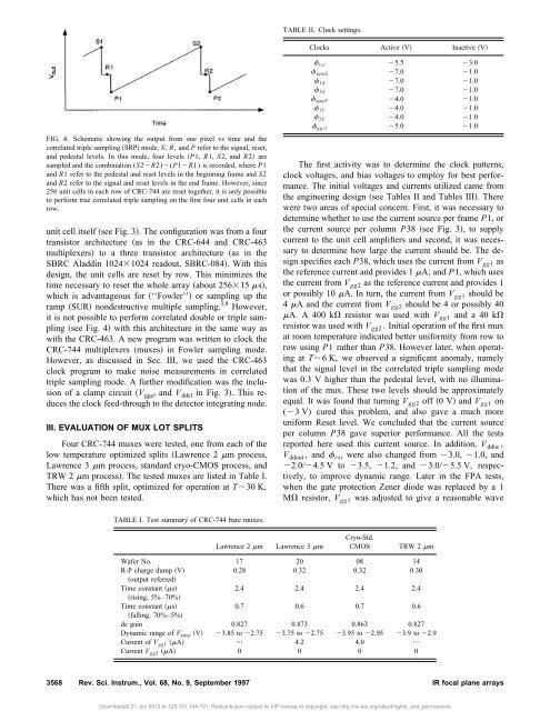
TABLE II. Clock settings.Clocks Active V Inactive VFIG. 4. Schematic showing the output from one pixel vs time and thecorrelated triple sampling SRP mode. S, R, and P refer to the signal, reset,and pedestal levels. In this mode, four levels P1, R1, S2, and R2 aresampled and the combination (S2R2)(P1R1) is recorded, where P1and R1 refer to the pedestal and reset levels in the beginning frame and S2and R2 refer to the signal and reset levels in the end frame. However, since256 unit cells in each row <strong>of</strong> CRC-744 are reset together, it is only possibleto per<strong>for</strong>m true correlated triple sampling on the first four unit cells in eachrow.unit cell itself see Fig. 3. The configuration was from a fourtransistor architecture as in the CRC-644 and CRC-463multiplexers to a three transistor architecture as in theSBRC Aladdin 10241024 readout, SBRC-084. With thisdesign, the unit cells are reset by row. This minimizes thetime necessary to reset the whole array about 25615 s,which is advantageous <strong>for</strong> ‘‘Fowler’’ or sampling up theramp SUR nondestructive multiple sampling. 3,8 However,it is not possible to per<strong>for</strong>m correlated double or triple samplingsee Fig. 4 with this architecture in the same way aswith the CRC-463. A new program was written to clock theCRC-744 multiplexers muxes in Fowler sampling mode.However, as discussed in Sec. III, we used the CRC-463clock program to make noise measurements in correlatedtriple sampling mode. A further modification was the inclusion<strong>of</strong> a clamp circuit V ggcl and V ddcl in Fig. 3. This reducesthe clock feed-through to the detector integrating node.III. EVALUATION OF MUX LOT SPLITSFour CRC-744 muxes were tested, one from each <strong>of</strong> thelow temperature optimized splits Lawrence 2 m process,Lawrence 3 m process, standard cryo-CMOS process, andTRW 2 m process. The tested muxes are listed in Table I.There was a fifth split, optimized <strong>for</strong> operation at T30 K,which has not been tested. rst 5.5 3.0 syncS 7.0 1.0 1S 7.0 1.0 2S 7.0 1.0 syncF 4.0 1.0 1F 4.0 1.0 2F 4.0 1.0 ggcl 5.0 1.0The first activity was to determine the clock patterns,clock voltages, and bias voltages to employ <strong>for</strong> best per<strong>for</strong>mance.The initial voltages and currents utilized came fromthe engineering design see Tables II and Tables III. Therewere two areas <strong>of</strong> special concern. First, it was necessary todetermine whether to use the current source per frame P1, orthe current source per column P38 see Fig. 3, to supplycurrent to the unit cell amplifiers and second, it was necessaryto determine how large the current should be. The designspecifies each P38, which uses the current from V gg1 asthe reference current and provides 1 A; and P1, which usesthe current from V gg2 as the reference current and provides 1or possibly 10 A. In turn, the current from V gg1 should be4 A and the current from V gg2 should be 4 or possibly 40A. A 400 k resistor was used with V gg1 anda40kresistor was used with V gg2 . Initial operation <strong>of</strong> the first muxat room temperature indicated better uni<strong>for</strong>mity from row torow using P1 rather than P38. However later, when operatingat T6 K, we observed a significant anomaly, namelythat the signal level in the correlated triple sampling modewas 0.3 V higher than the pedestal level, with no illumination<strong>of</strong> the mux. These two levels should be approximatelyequal. It was found that turning V gg2 <strong>of</strong>f 0 Vand V gg1 on(3 V) cured this problem, and also gave a much moreuni<strong>for</strong>m Reset level. We concluded that the current sourceper column P38 gave superior per<strong>for</strong>mance. All the testsreported here used this current source. In addition, V dduc ,V ddout , and rst were also changed from 3.0, 1.0, and2.0/4.5 V to 3.5, 1.2, and 3.0/5.5 V, respectively,to improve dynamic range. Later in the FPA tests,when the gate protection Zener diode was replaced by a 1M resistor, V gg1 was adjusted to give a reasonable waveTABLE I. Test summary <strong>of</strong> CRC-744 bare muxes.Lawrence 2 mLawrence 3 mCryo-Std.CMOSTRW 2 mWafer No. 17 20 08 14R-P charge dump V0.28 0.32 0.32 0.30output referredTime constant s2.4 2.4 2.4 2.4rising, 5%–70%Time constant s0.7 0.6 0.7 0.6falling, 70%–5%dc gain 0.827 0.873 0.863 0.827Dynamic range <strong>of</strong> V rstuc V 3.85 to 2.75 3.75 to 2.75 3.95 to 2.95 3.9 to 2.9Current <strong>of</strong> V gg1 A ••• 4.2 4.0 •••Current V gg2 A 0 0 0 03568 Rev. Sci. Instrum., Vol. 68, No. 9, September 1997 IR <strong>focal</strong> <strong>plane</strong> <strong>arrays</strong>Downloaded 21 Jun 2012 to 128.151.144.191. Redistribution subject to AIP license or copyright; see http://rsi.aip.org/about/rights_and_permissions
TABLE III. Bias setting.Biases Volt I park A a I flat A aV gg14.2 bV gg2 0.0V dduc 3.5 105V ssS 1.0V ssF 1.0V ddcl 1.9 105V ddout 1.2 260 270V ss1 ,V ss2 1.0 105 105V rstuc 3.5V detcV rstuc V biasV sub 0.0a Only currents more than 20 A are noted.b To provide 3.0 V at the chip carrier.c V bias is the applied back bias voltage across the photodiodes. For baremuxes. V bias 0 V. For CRC744-40716, V bias 400 mV.<strong>for</strong>m and dynamic range at the output, while maintaining lowpower dissipation. The unit cell current employed was about0.4 A. In Table III, the V dduc current when running flat outis the sum <strong>of</strong> the unit cell current from 256 unit cells. Thisis considerably lower than the 1 A employed <strong>for</strong> the baremux tests. In Table I, the V gg1 current is four times the unitcell current. This may explain the improved stability observedwith the FPAs compared with the bare muxes.The next significant problem was resetting in the Fowlersampling mode: in this mode, the array is reset and the average<strong>of</strong> n pedestal levels are subtracted from the average <strong>of</strong>n signal levels in the same integration ramp. The techniqueinitially used was to hold the reset clock on while clockingthrough all the rows, then turning it <strong>of</strong>f. However, it wasfound that the Fowler pedestal and signal levels were significantlydifferent from those seen in the correlated triple samplingmode, which cannot be correct. It was found thatproper resetting in the Fowler sampling mode required selectinga row, then turning the reset clock on <strong>for</strong> 15 s,then turning it <strong>of</strong>f, then selecting the next row. With thisclocking, the Fowler pedestal and signal levels were quitecomparable to those seen with correlated triple sampling. Ifone studies the schematic <strong>for</strong> the unit cell in Fig. 3, it makessense that just holding the reset clock ON while enablingsucceeding rows is not a good idea, since this could leave thereset field-effect transistor FET <strong>of</strong> each unit cell in an ONstate. After resetting, we want this FET to be in the OFFstate, to allow the integrating node to debias from dark currentand photocurrent.The tests concentrated on the Fowler sampling mode. Asshown in Figs. 5c and 5d, this mode can lead to significantlyreduced noise. All previous muxes we have testedshowed poor per<strong>for</strong>mance in Fowler sampling mode at temperaturesbelow about 23 K. 7 We also measured noise in thecorrelated triple sampling mode signal-reset-pedestal SRPmode in our s<strong>of</strong>tware to compare with previous measurements<strong>of</strong> the CRC-590 and 644 muxes and also to evaluatethis mode at low temperatures, in case the Fowler samplingmode proved to be unstable as it had <strong>for</strong> the CRC-590 and644 muxes. Finally, the reset mode R-G in our s<strong>of</strong>twarewas also tested to check out the noise <strong>of</strong> the FETs with theunit cell gate the gate <strong>of</strong> P2 in Fig. 3 held at the resetvoltage V rstuc . In Fowler and correlated triple samplingmodes, we are sensitive to noise with that gate floating thereset FET turned <strong>of</strong>f.For correlated triple sampling Fig. 4 and R-G modes,our old clock program <strong>for</strong> the CRC-463, 590, and 644 wasused. This would not be correct <strong>for</strong> actual array operation,since each unit cell is being reset 64 times, and only the firstfour pixels in each row have the correct integration time.However, we believe this to be a reasonable expedient whenthere is no signal or dark current, and we are just measuringthe noise. When checking <strong>for</strong> response to visible light in theSRP mode, only the first four pixels <strong>of</strong> each row showed alarge response.The procedure employed was to cool to 5.5 K. Thenthe steps followed were:1 operate the mux and confirm reasonable operation;2 check the last row and last column diagnostic lines toverify correct operation <strong>of</strong> the shift registers;3 measure the gain by measuring the output voltage as afunction <strong>of</strong> the reset voltage (V rstuc );4 shine optical light on the array and verify reasonableresponse positive signals were seen;5 take data with 6 s integration times as the Dewar warmsup liquid helium runs out.Two frames <strong>of</strong> data each in the SRP, R-G, Fowler-1,Fowler-8, and Fowler-32 were acquired Fowler-n refers toFowler sampling with n pairs <strong>of</strong> samples. Successive framesin the same mode were subtracted and a 2525 region nearthe center <strong>of</strong> the array was analyzed. After correcting <strong>for</strong> the& factor <strong>for</strong> the two data frames, the rms noise in this regiongives the pixel read noise. The average difference betweenthe two frames, which should be close to zero, was examinedin order to investigate instability, commonly seen in Fowlersampling mode at the lower temperatures. The bias framesshort integration dark current frames were also studied.Bias frames should be zero <strong>for</strong> Fowler mode; nonzero valuesindicate some instability. The SRP bias frame should also beclose to zero. The R-G bias frame includes an arbitrary dc<strong>of</strong>fset. It is examined to look <strong>for</strong> any drastic shifts in theoperating point <strong>of</strong> the FETs, <strong>for</strong> example, caused by freezeout.The 2525 region examined was positioned near arraycenter. For Lawrence 2 m material and TRW 2 m material,it was centered at row,column128,128. For theother two muxes it was centered at row,column100,100to avoid a bad pixel. The conversion from measured ADUsto voltage referred to the input was based on the measureddc gain, our gain <strong>of</strong> 20 preamplifiers, and the fact that 10-V<strong>for</strong> our analog digital converters ADCs gives 32 768 analogdigital units ADUs. The conversion to electrons was basedon the estimated node capacitance without detectors <strong>of</strong> 27.7fF from the engineering design. Figure 5 shows the noisemeasurement results. Figure 6 illustrates the instability testresults <strong>for</strong> Fowler mode with 32 sample pairs.From our bare mux data, Lawrence 2 m material appearedto be superior. Above 18 K, Fowler sampling modesappear well-behaved and the noise with 32 pairs <strong>of</strong> samplesRev. Sci. Instrum., Vol. 68, No. 9, September 1997IR <strong>focal</strong> <strong>plane</strong> <strong>arrays</strong>3569Downloaded 21 Jun 2012 to 128.151.144.191. Redistribution subject to AIP license or copyright; see http://rsi.aip.org/about/rights_and_permissions