Design of Low Cost Modem Using Tele Typewriter Signals - Ijcns.com
Design of Low Cost Modem Using Tele Typewriter Signals - Ijcns.com
Design of Low Cost Modem Using Tele Typewriter Signals - Ijcns.com

You also want an ePaper? Increase the reach of your titles
YUMPU automatically turns print PDFs into web optimized ePapers that Google loves.
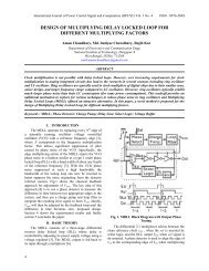
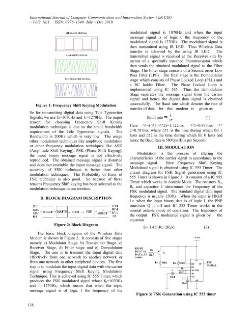
International Journal <strong>of</strong> Computer Communication and Information System ( IJCCIS)– Vol2. No1. ISSN: 0976–1349 July – Dec 2010Figure 1: Frequency Shift Keying ModulationSo for transmitting digital data using <strong>Tele</strong> <strong>Typewriter</strong><strong>Signals</strong>, we use f H=1070Hz and f L=1270Hz. The majorreason for choosing Frequency Shift Keyingmodulation technique is due to the small bandwidthrequirement <strong>of</strong> the <strong>Tele</strong> <strong>Typewriter</strong> signals. TheBandwidth is 200Hz which is very low. The usageother modulation techniques like amplitude modulationor other frequency modulation techniques like ASK(Amplitude Shift Keying), PSK (Phase Shift Keying),the input binary message signal is not effectivelyreproduced. The obtained message signal is distortedand does not resemble the input message signal. Theaccuracy <strong>of</strong> FSK technique is better than othermodulation techniques. The Probability <strong>of</strong> Error <strong>of</strong>FSK technique is also good. So because <strong>of</strong> thesereasons Frequency Shift keying has been selected as themodulation technique in our modem.II. BLOCK DIAGRAM DESCRIPTIONFigure 2: Block DiagramThe basic block diagram <strong>of</strong> the Wireless Data<strong>Modem</strong> is shown in Figure 2. It consists <strong>of</strong> five stagesnamely a) Modulator Stage, b) Transmitter Stage, c)Receiver Stage, d) Filter stage and e) DemodulatorStage. The aim is to transmit the Input digital dataeffectively from one network to another network orfrom one network to other peripheral devices. The firststep is to modulate the input digital data with the carriersignal using Frequency Shift Keying ModulationTechnique. This is achieved using IC 555 Timer, whichproduces the FSK modulated signal whose f H=1070Hzand f L=1270Hz, which means that when the inputmessage signal is <strong>of</strong> logic 1 the frequency <strong>of</strong> themodulated signal is 1070Hz and when the inputmessage signal is <strong>of</strong> logic 0 the frequency <strong>of</strong> themodulated signal is 1270Hz. The modulated signal isthen transmitted using IR LED. Thus Wireless Datatransfer is achieved by the using IR LED. Thetransmitted signal is received at the Receiver side bymeans <strong>of</strong> a spectrally matched Phototransistor whichthen sends the obtained modulated signal to the FilterStage. The Filter stage consists <strong>of</strong> a Second order <strong>Low</strong>Pass Filter (LPF). The final stage is the Demodulatorstage which consists <strong>of</strong> Phase Locked Loop (PLL) anda RC ladder Filter. The Phase Locked Loop isimplemented using IC 565. Thus the demodulatorStage separates the message signal from the carriersignal and hence the digital data signal is obtainedsuccessfully. The Baud rate which denotes the rate <strong>of</strong>transfer <strong>of</strong> data for this modem is given asBaud rate (1)Here =( 1+ 2)=1.722ms, 1=0.935ms,2=0.787ms, where 1 is the time during which bit 1lasts and 2 is the time during which bit 0 lasts andhence the Baud Rate is 580 bps (Bits per Second).III. MODULATIONModulation is the process <strong>of</strong> altering thecharacteristics <strong>of</strong> the carrier signal in accordance to themessage signal. Here Frequency Shift KeyingModulated signal is obtained using IC 555 Timer. Thecircuit diagram for FSK Signal generation using IC555 Timer is shown in Figure 3. It consists <strong>of</strong> a IC 555Timer which works in Astable Mode. The resistors R a,R b and capacitor C determines the Frequency <strong>of</strong> theFSK modulated signal. The standard digital data inputfrequency is usually 150Hz. When the input is HIGHi.e. when the input binary data is <strong>of</strong> logic 1, the PNPtransistor Q is <strong>of</strong>f and IC 555 Timer works in thenormal astable mode <strong>of</strong> operation. The frequency <strong>of</strong>the output FSK modulated signal is given by theequationf 0= 1.45/(R a+2R b)C (2)Figure 3: FSK Generation using IC 555 timer138