Design of Low Cost Modem Using Tele Typewriter Signals - Ijcns.com
Design of Low Cost Modem Using Tele Typewriter Signals - Ijcns.com
Design of Low Cost Modem Using Tele Typewriter Signals - Ijcns.com

You also want an ePaper? Increase the reach of your titles
YUMPU automatically turns print PDFs into web optimized ePapers that Google loves.
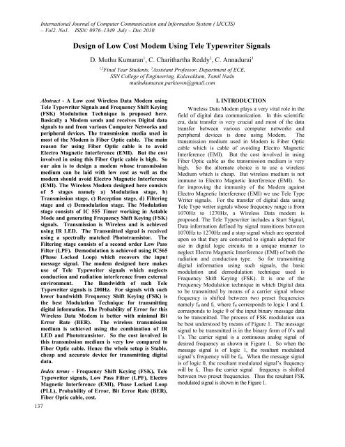
International Journal <strong>of</strong> Computer Communication and Information System ( IJCCIS)– Vol2. No1. ISSN: 0976–1349 July – Dec 2010<strong>Design</strong> <strong>of</strong> <strong>Low</strong> <strong>Cost</strong> <strong>Modem</strong> <strong>Using</strong> <strong>Tele</strong> <strong>Typewriter</strong> <strong>Signals</strong>D. Muthu Kumaran 1 , C. Charithartha Reddy 2 , C. Annadurai 31,2Final Year Students, 3 Assistant Pr<strong>of</strong>essor, Department <strong>of</strong> ECE,SSN College <strong>of</strong> Engineering, Kalavakkam, Tamil Nadumuthukumaran.parktown@gmail.<strong>com</strong>Abstract - A <strong>Low</strong> cost Wireless Data <strong>Modem</strong> using<strong>Tele</strong> <strong>Typewriter</strong> <strong>Signals</strong> and Frequency Shift Keying(FSK) Modulation Technique is proposed here.Basically a <strong>Modem</strong> sends and receives Digital datasignals to and from various Computer Networks andperipheral devices. The transmission media used inmost <strong>of</strong> the <strong>Modem</strong> is Fiber Optic cable. The mainreason for using Fiber Optic cable is to avoidElectro Magnetic Interference (EMI). But the costinvolved in using this Fiber Optic cable is high. Soour aim is to design a modem whose transmissionmedium can be laid with low cost as well as themodem should avoid Electro Magnetic Interference(EMI). The Wireless <strong>Modem</strong> designed here consists<strong>of</strong> 5 stages namely a) Modulation stage, b)Transmission stage, c) Reception stage, d) Filteringstage and e) Demodulation stage. The Modulationstage consists <strong>of</strong> IC 555 Timer working in AstableMode and generating Frequency Shift Keying (FSK)signals. Transmission is Wireless and is achievedusing IR LED. The Transmitted signal is receivedusing a spectrally matched Phototransistor. TheFiltering stage consists <strong>of</strong> a second order <strong>Low</strong> PassFilter (LPF). Demodulation is achieved using IC565(Phase Locked Loop) which recovers the inputmessage signal. The modem designed here makesuse <strong>of</strong> <strong>Tele</strong> <strong>Typewriter</strong> signals which neglectsconduction and radiation interference from externalenvironment. The Bandwidth <strong>of</strong> such <strong>Tele</strong><strong>Typewriter</strong> signals is 200Hz. For signals with suchlower bandwidth Frequency Shift Keying (FSK) isthe best Modulation Technique for transmittingdigital information. The Probability <strong>of</strong> Error for thisWireless Data <strong>Modem</strong> is better with minimal BitError Rate (BER). The wireless transmissionmedium is achieved using the <strong>com</strong>bination <strong>of</strong> IRLED and Phototransistor. So the cost involved inthis transmission medium is very low <strong>com</strong>pared toFiber Optic cable. Hence the whole setup is Stable,cheap and accurate device for transmitting digitaldata.137Index terms - Frequency Shift Keying (FSK), <strong>Tele</strong><strong>Typewriter</strong> signals, <strong>Low</strong> Pass Filter (LPF), ElectroMagnetic Interference (EMI), Phase Locked Loop(PLL), Probability <strong>of</strong> Error, Bit Error Rate (BER),Fiber Optic cable, cost.I. INTRODUCTIONWireless Data <strong>Modem</strong> plays a very vital role in thefield <strong>of</strong> digital data <strong>com</strong>munication. In this scientificera, data transfer is very crucial and most <strong>of</strong> the datatransfer between various <strong>com</strong>puter networks andperipheral devices is done using <strong>Modem</strong>. Thetransmission medium used in <strong>Modem</strong> is Fiber Opticcable which is cable <strong>of</strong> avoiding Electro MagneticInterference (EMI). But the cost involved in usingFiber Optic cable as the transmission medium is veryhigh. So the alternate choice is to use a wirelessMedium which is cheap. But wireless medium is notimmune to Electro Magnetic Interference (EMI). S<strong>of</strong>or improving the immunity <strong>of</strong> the <strong>Modem</strong> againstElectro Magnetic Interference (EMI) we use <strong>Tele</strong> TypeWriter signals. For the transfer <strong>of</strong> digital data using<strong>Tele</strong> Type writer signals whose frequency range is from1070Hz to 1270Hz, a Wireless Data modem isproposed. The <strong>Tele</strong> <strong>Typewriter</strong> includes a Start Signal,Data information defined by signal transitions between1070Hz to 1270Hz and a stop signal which are operatedupon so that they are converted to signals adopted foruse in digital logic circuits in a unique manner toneglect Electro Magnetic Interference (EMI) <strong>of</strong> both theradiation and conduction type. So for transmittingdigital information using such signals, the basicmodulation and demodulation technique used isFrequency Shift Keying (FSK). It is one <strong>of</strong> theFrequency Modulation technique in which Digital datato be transmitted by means <strong>of</strong> a carrier signal whosefrequency is shifted between two preset frequenciesnamely f H and f L, where f H corresponds to logic 1 and f Lcorresponds to logic 0 <strong>of</strong> the input binary message datato be transmitted. The process <strong>of</strong> FSK modulation canbe best understood by means <strong>of</strong> Figure 1. The messagesignal to be transmitted is in the binary form <strong>of</strong> 0’s and1’s. The carrier signal is a continuous analog signal <strong>of</strong>desired frequency as shown in Figure 1. So when themessage signal is <strong>of</strong> logic 1, the resultant modulatedsignal’s frequency will be f H. When the message signalis <strong>of</strong> logic 0, the resultant modulated signal’s frequencywill be f L. Thus the carrier signal frequency is shiftedbetween two preset frequencies. Thus the resultant FSKmodulated signal is shown in the Figure 1.
International Journal <strong>of</strong> Computer Communication and Information System ( IJCCIS)– Vol2. No1. ISSN: 0976–1349 July – Dec 2010Figure 1: Frequency Shift Keying ModulationSo for transmitting digital data using <strong>Tele</strong> <strong>Typewriter</strong><strong>Signals</strong>, we use f H=1070Hz and f L=1270Hz. The majorreason for choosing Frequency Shift Keyingmodulation technique is due to the small bandwidthrequirement <strong>of</strong> the <strong>Tele</strong> <strong>Typewriter</strong> signals. TheBandwidth is 200Hz which is very low. The usageother modulation techniques like amplitude modulationor other frequency modulation techniques like ASK(Amplitude Shift Keying), PSK (Phase Shift Keying),the input binary message signal is not effectivelyreproduced. The obtained message signal is distortedand does not resemble the input message signal. Theaccuracy <strong>of</strong> FSK technique is better than othermodulation techniques. The Probability <strong>of</strong> Error <strong>of</strong>FSK technique is also good. So because <strong>of</strong> thesereasons Frequency Shift keying has been selected as themodulation technique in our modem.II. BLOCK DIAGRAM DESCRIPTIONFigure 2: Block DiagramThe basic block diagram <strong>of</strong> the Wireless Data<strong>Modem</strong> is shown in Figure 2. It consists <strong>of</strong> five stagesnamely a) Modulator Stage, b) Transmitter Stage, c)Receiver Stage, d) Filter stage and e) DemodulatorStage. The aim is to transmit the Input digital dataeffectively from one network to another network orfrom one network to other peripheral devices. The firststep is to modulate the input digital data with the carriersignal using Frequency Shift Keying ModulationTechnique. This is achieved using IC 555 Timer, whichproduces the FSK modulated signal whose f H=1070Hzand f L=1270Hz, which means that when the inputmessage signal is <strong>of</strong> logic 1 the frequency <strong>of</strong> themodulated signal is 1070Hz and when the inputmessage signal is <strong>of</strong> logic 0 the frequency <strong>of</strong> themodulated signal is 1270Hz. The modulated signal isthen transmitted using IR LED. Thus Wireless Datatransfer is achieved by the using IR LED. Thetransmitted signal is received at the Receiver side bymeans <strong>of</strong> a spectrally matched Phototransistor whichthen sends the obtained modulated signal to the FilterStage. The Filter stage consists <strong>of</strong> a Second order <strong>Low</strong>Pass Filter (LPF). The final stage is the Demodulatorstage which consists <strong>of</strong> Phase Locked Loop (PLL) anda RC ladder Filter. The Phase Locked Loop isimplemented using IC 565. Thus the demodulatorStage separates the message signal from the carriersignal and hence the digital data signal is obtainedsuccessfully. The Baud rate which denotes the rate <strong>of</strong>transfer <strong>of</strong> data for this modem is given asBaud rate (1)Here =( 1+ 2)=1.722ms, 1=0.935ms,2=0.787ms, where 1 is the time during which bit 1lasts and 2 is the time during which bit 0 lasts andhence the Baud Rate is 580 bps (Bits per Second).III. MODULATIONModulation is the process <strong>of</strong> altering thecharacteristics <strong>of</strong> the carrier signal in accordance to themessage signal. Here Frequency Shift KeyingModulated signal is obtained using IC 555 Timer. Thecircuit diagram for FSK Signal generation using IC555 Timer is shown in Figure 3. It consists <strong>of</strong> a IC 555Timer which works in Astable Mode. The resistors R a,R b and capacitor C determines the Frequency <strong>of</strong> theFSK modulated signal. The standard digital data inputfrequency is usually 150Hz. When the input is HIGHi.e. when the input binary data is <strong>of</strong> logic 1, the PNPtransistor Q is <strong>of</strong>f and IC 555 Timer works in thenormal astable mode <strong>of</strong> operation. The frequency <strong>of</strong>the output FSK modulated signal is given by theequationf 0= 1.45/(R a+2R b)C (2)Figure 3: FSK Generation using IC 555 timer138
International Journal <strong>of</strong> Computer Communication and Information System ( IJCCIS)– Vol2. No1. ISSN: 0976–1349 July – Dec 2010The Resistors R a, R b and capacitor C are selected insuch a way that the value <strong>of</strong> f 0 is 1070Hz. The circuitdiagram when the input is HIGH is shown inthe Figure 4.Figure 6: FSK modulated signalIV. TRANSMISSIONFigure 4: When the Input is HIGHHere the values <strong>of</strong> R a= 50K ohm, R b= 47K ohmand C=10nF. When the input is LOW i.e. when theinput binary data is <strong>of</strong> logic 0, the PNP transistor Q ison and its connects the resistance R c across theresistance R a. Thus now the frequency <strong>of</strong> the outputFSK modulated signal is given by the equationf 0= 1.45/((R a||R c)+2R b)C (3)The Resistors Rc is selected in such a way that thevalue <strong>of</strong> f 0 is 1270Hz. The circuit diagram when theinput is LOW is shown in the Figure 5. Herethe value <strong>of</strong> R c=50K ohm. The capacitor C1 is used tobypass noise and ripples from the supply. The resultantFSK modulated signal along with the digital binaryinput data at 150Hz is shown in the Figure 6. From theFigure 6 it is evident that during logic 1 <strong>of</strong> the binaryinput data f H=1070Hz and during logic 0 <strong>of</strong> the binaryinput data f L=1270Hz. Thus the Frequency ShiftKeying (FSK) modulated signal is obtained from themodulator stage.Figure 7: IR LED emitterAn infrared emitter is an LED made from GalliumArsenide, which emits near-infrared energy at about880nm. The Frequency Shift Keying signal from theModulator is now wirelessly transmitted to the receiverside using IR LED. The IR LED used as a transmitteris shown in figure 7. The circuit diagram for thisprocess is shown in figure 8. The value <strong>of</strong> the limitingResistor R is calculatedFigure 8: Transmitter using IR LEDusing the formula(4)Here Supply voltage V s is 5V, LED Voltage drop V f is3.3V and LED current rating I f is 20mA. Hence thevalue <strong>of</strong> R is 85 ohms.Figure 5: When the Input is LOW139
International Journal <strong>of</strong> Computer Communication and Information System ( IJCCIS)– Vol2. No1. ISSN: 0976–1349 July – Dec 2010V. RECEPTIONFigure 9: Phototransistor DetectorThe infrared Phototransistor acts as a transistorwith the base voltage determined by the amount <strong>of</strong> lighthitting the transistor. Hence it acts as a variable currentsource. Greater amount <strong>of</strong> IR light cause greatercurrent to flow through the collector-emitter leads. Thesignal from the Transmitter side should be received atthe Receiver side by a spectrally matchedPhototransistor. The Phototransistor used as a Receiveris shown in the figure 9. The circuit diagram for thisprocess is shown in figure 10. Thus the whole process<strong>of</strong> wireless transfer <strong>of</strong> data is achieved using the<strong>com</strong>bination <strong>of</strong> IR LED and a spectrally matchedPhototransistor. This wireless transmission channel ischeaper in <strong>com</strong>parison to the transmission mediumobtained using Fiber Optic cable. The importantparameter for a <strong>Modem</strong>, which is the Probability <strong>of</strong>Error is good for this <strong>com</strong>bination <strong>of</strong> IR LED andphototransistor.Figure 10: Receiver using PhototransistorVI. FILTERThe <strong>Low</strong> Pass Filter (LPF) is used to eliminate theunnecessary high frequency <strong>com</strong>ponents from any lowfrequency signal and hence helps in improving theProbability <strong>of</strong> Error <strong>of</strong> a System. Here a second orderLPF as shown in the figure 11 is used to remove thehigh frequency Noise <strong>com</strong>ponents introduced by theWireless Channel. The timing resistors are calculatedusing the following formulaef L=1/(2*pi*R 1*C 1) (5)f H=1/(2*pi*R 2*C 2) (6)So for f L=1070Hz and f H=1270Hz, we get R 1=745 ohm,R 2=1.25K ohm, C 1=200nF, C 2=100nF.Figure 11: <strong>Low</strong> Pass FilterVII. DEMODULATIONThe process <strong>of</strong> eliminating the Carrier signal andrecovering the base band message signal from themodulated signal is termed as Demodulation. Here theprocess <strong>of</strong> demodulation is achieved using PhaseLocked Loop (PLL) IC 565. The circuit diagram forachieving the process <strong>of</strong> demodulation using PLL IC565 is shown in figure 12. In the 565 PLL thefrequency shift is usually ac<strong>com</strong>plished by driving aVoltage Controlled Oscillator (VCO) with the digitaldata signal so that the two resulting frequencies correspondto the logic 0 and logic 1 states <strong>of</strong> the digital datasignal. The frequencies corresponding to logic 1 andlogic 0 states are <strong>com</strong>monly called the mark and spacefrequencies. The demodulator receives a signal at one<strong>of</strong> the two distinct carrier frequencies 1,270 Hz or1,070 Hz representing logic levels <strong>of</strong> mark (- 5 V) orspace (+ 14 V), respectively. Capacitance coupling isused at the input to remove a dc level. As the signalappears at the input <strong>of</strong> 565 PLL, the PLL locks to theinput frequency and tracks it between the two possiblefrequencies with a corresponding dc shift at the output.Resistor R 1 and capacitor C 1 determine the free-runningfrequency <strong>of</strong> the VCO. Capacitor C 2 is a loop filtercapacitor that establishes the dynamic characteristics <strong>of</strong>the demodulator. Capacitor C 2 is chosen smaller thanusual one to eliminate overshoot on the output pulse. Athree-stage RC ladder filter is employed for removingthe sum frequency <strong>com</strong>ponent from the output. TheVCO frequency is adjusted with R 1 so that the dcvoltage level at the output (pin 7) is the same as that atpin 6. An input at frequency 1,070 Hz drives thedemodulator output voltage to a more positive voltagelevel, driving the digital output to the high level (spaceor + 14 V). An input at 1,270 Hz correspondinglydrives the 565 dc output less positive with the digitaloutput, which then drops to the low level (mark or – 5V). The <strong>com</strong>parator prevents the amplitude changesoccurring at the output stage. Thus the demodulatorstage effectively reproduces the input digital data at150Hz. The resultant digital data signal obtained fromthe FSK signal by the Demodulation process is shownin figure 13.140
International Journal <strong>of</strong> Computer Communication and Information System ( IJCCIS)– Vol2. No1. ISSN: 0976–1349 July – Dec 2010Figure 12: Demodulator using PLL 565Figure 13: Input Digital data from FSK signalVIII. PROBABILITY OF ERRORThe most important parameter that defines theefficiency <strong>of</strong> a <strong>Modem</strong> is the Probability <strong>of</strong> Error andBit Error Rate (BER). BER means the amount <strong>of</strong> errorintroduced in the transmitted signal by the channel’snoise. Usually the noise considered in a wirelessmedium is Additive White Gaussian Noise with zeromean and power Spectral density as N o/2. Theexpression for Probability <strong>of</strong> Error for this wireless datamodem which uses Non Coherent FSK demodulation isgiven asp e=1/2*exp(-E b/(2*N o)) (7)where E b is the transmitted signals energy per bit. Theplot <strong>of</strong> Probability <strong>of</strong> Error and E b/N o is shown inFigure 14. From the Figure 14 it is very clear that theBit Error Rate (BER) for this wireless data <strong>Modem</strong> isvery low.Figure 14: Bit Error Rate (BER)IX. CONCLUSIONThus in this paper a <strong>Low</strong> cost Wireless Data<strong>Modem</strong> using <strong>Tele</strong> <strong>Typewriter</strong> signals and FrequencyShift Keying (FSK) Modulation and Demodulationtechnique is designed and its importance to transmitdigital data wirelessly with minimal Bit Error Rate(BER) without getting affected by Electro MagneticInterference (EMI) <strong>of</strong> conduction and radiation typefrom the external environment is analyzed.X. REFERENCE[1]. Tom McDermott, Wireless Digital Communications: <strong>Design</strong>and Theory, Tucson Amateur Packet Radio Corporation,Tucson, Arizona, 1996.[2]. Peyton Z. Peebles, Digital Communication Systems, Prentice-Hall, Englewood Cliffs, New Jersey, 1987.[3]. Smon Haykins, Communication Systems, John Wiley, 4 thEdition, 2001.[4]. Jhn G. Proakis, Digital Communication, McGraw Hill, 3 rdEdition, 1995.[5]. Tub & Schilling, Principles <strong>of</strong> Digital Communication, TataMcGraw-Hill, 28 th reprint, 2003.141