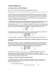
Schematic PCELL Implementation in Virtuoso Platform
Schematic PCELL Implementation in Virtuoso Platform
Schematic PCELL Implementation in Virtuoso Platform

You also want an ePaper? Increase the reach of your titles
YUMPU automatically turns print PDFs into web optimized ePapers that Google loves.
SCHEMATIC <strong>PCELL</strong> IMPLEMENTATION IN VIRTUOSO ® PLATFORMPRANAV BHUSHANCADENCE DESIGN SYSTEMS+91-120-2562842pbhushan@cadence.comRAJA MITRArmitra@cadence.comINTERNATIONAL CADENCE USERS GROUP CONFERENCESeptember 13-15, 2004Santa Clara, CAABSTRACT
Analog designers need compact and efficient libraries <strong>in</strong> custom IC design. This paper describes anapproach to reduce the number of physical variants of a library component us<strong>in</strong>g schematic parameterizedcells (pcells) <strong>in</strong> <strong>Virtuoso</strong>® Custom Design environment. Pcell technology makes the underly<strong>in</strong>g librarymore compact, versatile and dynamic with less number of variants for a s<strong>in</strong>gle component. We describepcell design us<strong>in</strong>g Cadence proprietary language (SKILL) and discuss some of the challenges faced byCAD eng<strong>in</strong>eers <strong>in</strong> its implementation along with solutions.To elucidate more on the challenges some well known pcell implementations like mtl<strong>in</strong>e, nport, scasubckt,ibis_buffer components etc. <strong>in</strong> analog library (analogLib) are considered. The repetitive challenges <strong>in</strong> pcellimplementation along with future enhancements to make it more robust are discussed.Keywords: SKILL, analogLib, CDF, pcell, simInfo
1 INTRODUCTION<strong>Virtuoso</strong>® <strong>Platform</strong> conta<strong>in</strong>s an analog design components library known as analogLib, which conta<strong>in</strong>sdifferent components that are widely used by analog designers <strong>in</strong> a variety of full custom analog and RF ICdesign. Analog library (analogLib) conta<strong>in</strong>s analog primitives, subcircuits of a wide variety rang<strong>in</strong>g from -active devices, analysis devices, passive elements, parasitics and sources (dependent, <strong>in</strong>dependent etc.).A parameterized cell, or pcell, is a graphic, programmable cell that allows to create a customized <strong>in</strong>stanceeach time it is placed or used <strong>in</strong> design. The term pcell can mostly be related <strong>in</strong> physical design spacewhere it is used to create layout views. A schematic pcell is a variant of a layout pcell, which can be used <strong>in</strong>schematic designs. <strong>Schematic</strong> pcells are used <strong>in</strong> front-end arena where they can simply <strong>in</strong>stantiated <strong>in</strong><strong>Virtuoso</strong>® Composer (<strong>Schematic</strong> Design Entry Tool) w<strong>in</strong>dow and easily netlisted and simulatedIn the follow<strong>in</strong>g section, motivation for schematic pcell creation is discussed <strong>in</strong> detail. This will be followedby extensive design level details for implement<strong>in</strong>g pcell. Lastly the challenges and future work related withpcell is discussed and improvements suggested.2 MOTIVATION AND HISTORYTraditional analog library components do not support variants of a s<strong>in</strong>gle component. In order to support allvariants of a component for example for a multi-port device (nport) device, different variants for each portshould be provided. These variants can have different types, start<strong>in</strong>g from s<strong>in</strong>gle port (n1port) device, totwo ports (n2port) device, three ports (n3port) device, four ports (n4port) etc. and so on. As aconsequence, this makes the underly<strong>in</strong>g library to conta<strong>in</strong> four components for a nport (assum<strong>in</strong>g we areprovid<strong>in</strong>g support for 4 variants) device namely n1port, n2port, n3port and n4port. This makes the librarymore bulky <strong>in</strong> terms of manag<strong>in</strong>g more number of components, more disk space utilization <strong>in</strong> terms ofstor<strong>in</strong>g different variants and more ma<strong>in</strong>tenance overhead <strong>in</strong> terms of revision control of all variants.With the grow<strong>in</strong>g demand of multi port/conductor/term<strong>in</strong>al components and wide variety of design p<strong>in</strong>s,term<strong>in</strong>als and shape requirements there was always a need for a s<strong>in</strong>gle customizable component thatcould easily be modified and used per designer’s need. The component should be versatile, work<strong>in</strong>gseamless <strong>in</strong> a design hav<strong>in</strong>g a wide variety of parameters and shape and should be easy to implement anduse. With such a request pcell came out to be the best choice. Other well known requirements for pcellcomponents are: multi-conductor transmission l<strong>in</strong>e (mtl<strong>in</strong>e) hav<strong>in</strong>g a large number of term<strong>in</strong>als, oftenrequired and used <strong>in</strong> RF and mixed-signal designs and the IBIS (I/O Buffer Information Specification)buffer component hav<strong>in</strong>g variation <strong>in</strong> its shape and p<strong>in</strong>s based on the type and mode of the buffer selected.Such components have a common requirement i.e. a change <strong>in</strong> p<strong>in</strong>s, shape, structure etc., and pcellseems to be an appropriate choice because it provides advantages <strong>in</strong> terms of mak<strong>in</strong>g a library morecompact, less bulky, more efficient and free from the overheads of ma<strong>in</strong>ta<strong>in</strong><strong>in</strong>g and stor<strong>in</strong>g differentsymbols for a s<strong>in</strong>gle component.Pcells date back to years when layout designers used them to adjust chip geometries and comb<strong>in</strong>ations <strong>in</strong>chip design. <strong>Schematic</strong> pcells recently came <strong>in</strong>to picture when people felt the need to extend the samefunctionality from layout to schematic doma<strong>in</strong>. Hav<strong>in</strong>g a potential solution <strong>in</strong> terms of a schematic pcell forvariants, the next challenge <strong>in</strong> its design is the appropriate netlist<strong>in</strong>g support. In early 2001 schematicpcells came to be supported by <strong>Virtuoso</strong>® OSS (Open Simulation System/netlisters) and this opened thedoors for current work and schematic pcells widely came <strong>in</strong>to use.More details on pcells and their implementation work which has already been done is discussed <strong>in</strong> nextsection.
3 DESIGN DETAILSTo create a new component <strong>in</strong> a library you need to create its symbol, its CDF (Component DescriptionFormat) parameters, simulation <strong>in</strong>formation and a netlist<strong>in</strong>g procedure (if the component does not has adefault netlist<strong>in</strong>g support). Details on pcell design are mentioned <strong>in</strong> [2] and [3]. Here we will briefly touchupon basic requirements for a schematic pcell design and its characteristics.3.1 Basic Pcell Structure and its implementationA parameterized cell or pcell exists at three different levels:• superMaster (which consists of SKILL code, parameter def<strong>in</strong>itions and default values; it resides ondisk);• subMaster (conta<strong>in</strong>s unique geometries produced by unique set of parameter values; resides <strong>in</strong> virtualmemory) and• <strong>in</strong>stance (derived from sub-master, <strong>in</strong>herits parameters from subMaster; resides <strong>in</strong> virtual memory).SuperMastersubMaster1 subMaster2 subMaster3. . . . . subMasterNI 1 I 2 I 3 I 4 I 5 I 6 I 7 I m-1 I mFigure 1: A Pcell structure consist<strong>in</strong>g of superMaster, subMaster and <strong>in</strong>stanceFigure[1], illustrates the super-master of a pcell component at the top and its different sub-masters, witheach sub-master represent<strong>in</strong>g different <strong>in</strong>stances of the pcell. e.g I 1 , I 2 ... I m used by a designer. Moredetails of these can be found <strong>in</strong> [2].3.1.1 Writ<strong>in</strong>g SKILL code to create a symbolOrd<strong>in</strong>ary schematic symbols are fixed and static but pcells are dynamic and more versatile as compared toschematic symbols. Special, accurate SKILL code is required to create and compile them [2]. Severaldatabase calls mentioned <strong>in</strong> [4] are used along with the pcell code. Pcell code is <strong>in</strong>dependent of theunderly<strong>in</strong>g databases i.e. C-level database access (CDBA) and OpenAccess (OA). Once written the samepcell code should work f<strong>in</strong>e <strong>in</strong> both CDBA and OA.The basic structure of a pcell SKILL code consists of:• Cell Identifier section: Consists of a list of library identifier(e.g. analogLib), cell name (i.e., name ofcomponent e.g. mtl<strong>in</strong>e), view name (symbol) and view type (type of view consists of maskLayout,schematic and schematicSymbol, here schematicSymbol). Here the type of pcell is def<strong>in</strong>ed - for aschematic pcell viewType must be equal to schematicSymbol.
• Parameter declaration section: This consists of a list of all formal parameters and their defaults. It isimportant to always def<strong>in</strong>e all defaults used <strong>in</strong> the pcell code, otherwise this may lead to malfunctions.• Actual body of pcell code: This is the core pcell skill code which is required for build<strong>in</strong>g geometries(shapes) and p<strong>in</strong>s, labels etc. for the pcell. Each and every entity of the component is described <strong>in</strong>terms of the database creation functions. For example a simple l<strong>in</strong>e is created via dbCreateL<strong>in</strong>e,rectangle is created via dbCreateRect, nets on the symbol are created via dbCreateNet, term<strong>in</strong>als viadbCreateTerm, labels via dbCreateLabel, p<strong>in</strong>s via dbCreateP<strong>in</strong> etc. Various database functions [4] areconta<strong>in</strong>ed <strong>in</strong> this portion of code. Special checks like the pcell shape, its limit, variant size etc. areprogrammed <strong>in</strong> this section only.A sample code snippet for mtl<strong>in</strong>e pcell component exist<strong>in</strong>g <strong>in</strong> analogLib is shown <strong>in</strong> Figure[2] as a sample.It should be <strong>in</strong>terpreted from the above pseudo-code that the pcell’s l<strong>in</strong>es, term<strong>in</strong>als, p<strong>in</strong>s etc. are all crepcDef<strong>in</strong>ePCell(list(ddGetObj("analogLib")"mtl<strong>in</strong>e" "symbol" "schematicSymbol")}((n 1)) (uselmg nil) }prog (............) ; end prog }) ; end pcDef<strong>in</strong>ePcellCell IdentifierParam declarationPcell bodyFigure 2: Structure of a sample pcell code3.1.2 Pseudo code for mtl<strong>in</strong>e pcellThe programm<strong>in</strong>g of the pcell, i.e., <strong>in</strong> case of mtl<strong>in</strong>e the change <strong>in</strong> number of p<strong>in</strong>s is described via CDFparameters, ‘n’ and ‘uselmg’. Here ‘n’ describes the number of p<strong>in</strong>s exclud<strong>in</strong>g the reference p<strong>in</strong>s, and’uselmg’ changes the mtl<strong>in</strong>e reference p<strong>in</strong>s with respect to the use subcircuit or non-subcircuit model. Thiscontrols the overall mtl<strong>in</strong>e structure to have an odd or even number of p<strong>in</strong>s.Based on selection of values of ’n’ and ’uselmg’ the component p<strong>in</strong>s can grow, shr<strong>in</strong>k and vary. Thepseudo code for this is illustrated below.1. Set pcDef<strong>in</strong>ePcell and def<strong>in</strong>e all cell identification parameters.2. Set defaults for formal parameters:• n=1• uselmg=nil3. If n and uselmg are not def<strong>in</strong>ed then set their values to defaults. Otherwise take values from thecomponent.4. Write SKILL code to create bound<strong>in</strong>g box, l<strong>in</strong>es, rectangle etc.5. Write SKILL to create l<strong>in</strong>es, rectangle etc. for p<strong>in</strong>s, term<strong>in</strong>als, labels etc. If uselmg=nil then create tworeference l<strong>in</strong>es (<strong>in</strong>ref/outref) else create a s<strong>in</strong>gle reference l<strong>in</strong>e (ref)6. For each I = 1 to n (where n = number of p<strong>in</strong>s other than the reference p<strong>in</strong>.• Create other desired p<strong>in</strong>s, their term<strong>in</strong>als, nets, labels etc.• end for loop7. Add cdsName
ated us<strong>in</strong>g ITKDB functions. First only the superMaster is created us<strong>in</strong>g defaults mentioned <strong>in</strong> SKILL codeand later based on the values of formal parameters (here, n and uselmg) the pcell’s required p<strong>in</strong>s are createdand or destroyed from the subMaster variants.This section is most error prone and any <strong>in</strong>correct steps here can lead to failures <strong>in</strong> pcell compilation process.So careful check<strong>in</strong>g and debugg<strong>in</strong>g should be done while writ<strong>in</strong>g pcell code. More details of thesecan be found <strong>in</strong> [2,3]3.1.3 Results of work doneTo understand more on this lets take the example multi-conductor transmission l<strong>in</strong>e (mtl<strong>in</strong>e) [5], componentwhere there are two formal parameters - variation <strong>in</strong> number of p<strong>in</strong>s (n) and use of sub-circuit component(uselmg). It should be noted that these formal parameters are exactly mapped to the component descriptionformat (CDF) parameters[1] on the symbol. Based on the values of ‘n’ and ‘uselmg’ the componentp<strong>in</strong>s can grow, shr<strong>in</strong>k and vary. This is illustrated <strong>in</strong> Figure[3].3(a). n=1, uselmg=nil3(b). n=1, uselmg=t3(c). n=5, uselmg=nilFigure 3: Different Pcell variants of mtl<strong>in</strong>e component
Tak<strong>in</strong>g another example of the ibis_buffer component, ref[6], where the shape and p<strong>in</strong>s of the entire componentcan change from a buffer to a <strong>in</strong>verted-buffer based on CDF parameters. In this case the CDFparameters are ‘bufferType’ and ‘bufferVariant’. The value of these is specified on the CDF of the pcell<strong>in</strong>stance and the shapes and p<strong>in</strong>s can vary.4 (a). BufferType=<strong>in</strong>putOutput, with differential <strong>in</strong>put p<strong>in</strong>sand external power4(b). Buffer Type=term<strong>in</strong>ator, with external_powerFigure 4: Pcell variants of IBIS_BufferFigure[4], shows an example of different ibis_buffer cells hav<strong>in</strong>g different shapes and number of p<strong>in</strong>s. Thisrequires special programm<strong>in</strong>g skills as well as the synchronization between the formal parameters and theshape of the pcell component.Most of the errors are done <strong>in</strong> this section and a careful check and debugg<strong>in</strong>g should be used for pcell programm<strong>in</strong>g.3.1.4 Mathematical analysisThe limitation of not us<strong>in</strong>g a pcell based implementation for the same component is that we will have a geometricnumber of <strong>in</strong>dependent unique variants to be ma<strong>in</strong>ta<strong>in</strong>ed <strong>in</strong> the library. Mathematically this can beexpla<strong>in</strong>ed as below.Let us consider a pcell with m formal parameters, where m belongs to a set of all natural numbers.Each of the pcell <strong>in</strong>stantiations can have their own set of variations <strong>in</strong> number of components.Let K 1 , K 2 , . . ., K k , . . . K m , be the variations of the formal parameters. Then the total number of variantsfor the pcell component would be def<strong>in</strong>ed as:
For the case as shown <strong>in</strong> Figure[3], there are 2 formal parameters (m=2) n and uselmg; where n variesfrom 1 to 5 (K 1 =5) and uselmg can have two values either true or false (K 2 =2).So, per the <strong>in</strong>ference made from derivation done <strong>in</strong> equation (1) we conclude that the mtl<strong>in</strong>e pcell, shown <strong>in</strong>e.g. 3(c), will have a total of= K 1 * K 2 = 5 * 2 = 10 variants.when, n varies from 1 to 5 and uselmg from t/nil.In contrast for a similar case <strong>in</strong> a non-pcell component this would require the creation of 10 separate librarycomponents which can be done via a s<strong>in</strong>gle ’mtl<strong>in</strong>e’ pcell.This shows the advantage and importance <strong>in</strong> usage of the pcell components.3.2 Add<strong>in</strong>g CDF parametersm∏i = 1Ki……………… ( 1)CDF (Component Description Format) parameters play an important role for any library component. Theseparameters are visible <strong>in</strong> the Edit Object Properties form <strong>in</strong> the <strong>Virtuoso</strong>® schematic composer w<strong>in</strong>dow.Various CDF parameters belong<strong>in</strong>g to the <strong>in</strong>stance are added here. These parameters are of differenttypes rang<strong>in</strong>g from str<strong>in</strong>g, <strong>in</strong>t, float, radio, cyclic, boolean, button etc. More details about the CDF parameterstheir usage and type is mentioned <strong>in</strong> [1].The parameters which are visible <strong>in</strong> the netlist (connectivity <strong>in</strong>formation of circuit) file are commonly calledas <strong>in</strong>stance parameters (<strong>in</strong>stParameters) and the ones which are not visible <strong>in</strong> netlist may belong to otherparameters (otherParameters). These parameters have a 1-1 mapp<strong>in</strong>g with the simulation <strong>in</strong>formation ofthe component and these are know from the simulators help or manuals.For a pcell care must be taken to ensure that the defaults between the CDF and the pcell must match.These CDF parameters have associated callbacks which perform the desired action on the mouse click orselection made by the user <strong>in</strong> the Edit Object Properties form.
Figure 5: Default CDF form for mtl<strong>in</strong>e componentFigure[5] shows a default CDF form for mtl<strong>in</strong>e component, note that the default CDF parameter values forn=1 and uselmg=nil. These values match with the snapshot shown <strong>in</strong> Figure[3a].3.3 Add<strong>in</strong>g Simulation Information and netlist<strong>in</strong>g supportSimulation <strong>in</strong>formation (simInfo) is necessary to simulate a component by a given simulator. This <strong>in</strong>formationis unique and specific for each simulator and is based on the simulator <strong>in</strong>ternal reference. Details onsimInfo are available <strong>in</strong> [1,5,6]. In general different categories are <strong>in</strong>cluded <strong>in</strong> simInfo section for a component<strong>in</strong>stParameters, otherParameters, componentName, termOrder, termMapp<strong>in</strong>g, propMapp<strong>in</strong>g, netlist-Procedure etc.
Pcells are different from primitive components <strong>in</strong> the sense that their term<strong>in</strong>als, p<strong>in</strong>s and shapes can varybased on the type of the CDF parameters chosen. In order to take care of all the variants, special netlist<strong>in</strong>gprocedures are used for pcells. The netlist<strong>in</strong>g procedure takes care of the formatter object and pr<strong>in</strong>ts the<strong>in</strong>stance CDF parameters based on the term<strong>in</strong>als, nets etc. connected to it. Netlist<strong>in</strong>g procedure should besmart enough to handle error conditions which might occur <strong>in</strong> case of a netlist generation from a user. Acommon example of such an error is the absence of the required <strong>in</strong>stance parameter on the device. Insuch cases netlister should flag an error message.3.4 How to identify a pcell componentThe ITKDB (Integrators Tool Kit Data Base) Guide[4] provides various db (database) calls which can beused.cv=dbOpenCellViewByType("analogLib" "res" "symbol")cv~>isParamCell=> nilcv1=dbOpenCellViewByType("analogLib" "mtl<strong>in</strong>e" "symbol")cv1~>isParamCell=> tOther PIs for dump<strong>in</strong>g and writ<strong>in</strong>g the pcell data from the database can be used. These are widely documentedand available for customers. Some of such functions <strong>in</strong>clude e.g. cdfDump, dbWriteSkill etc.4. LIMITATIONS, CHALLENGES AND FUTURE WORKThere are various safety rules which should be used while design<strong>in</strong>g schematic pcells. These details arementioned <strong>in</strong> [2]. Apart from them follow<strong>in</strong>g precautions should also be used while design<strong>in</strong>g schematicpcells:• Use msfb or PD doma<strong>in</strong> workbench. e.g. <strong>in</strong> icms you can not create a pcell.• Remember that <strong>in</strong> a pcell code no function can be re-def<strong>in</strong>ed, although you can do this for your localtest<strong>in</strong>g. In some cases this causes extra markers to show up on the schematic symbol and causecompilation failures• Remember to always use the fourth argument to the pcDef<strong>in</strong>ePcell of type equal to schematicSymbol,because by default pcDef<strong>in</strong>ePcell <strong>in</strong>fers the argument to be a masklayout type and this will causeproblems when you translate the CDBA pcell on OpenAccess database.• More precautions are listed <strong>in</strong> [2].There are a couple of limitations <strong>in</strong> the usage of pcells. First one is <strong>Virtuoso</strong>® AMS (Analog Mixed-Signal)product does not fully supports schematic pcells. Because it does not fully supports netlist<strong>in</strong>g of schematicpcell based designs. Another issue with pcell is the requirement of dynamic simInfo. Dynamic simInfo is anewer term which came <strong>in</strong>to existence with pcells. S<strong>in</strong>ce pcells can grow and shr<strong>in</strong>k <strong>in</strong> size so their termOrderand termMapp<strong>in</strong>g can not be static. In order to comply with this dynamic simInfo hav<strong>in</strong>g a vary<strong>in</strong>gsimInfo with respect to the component is required. If dynamic simInfo is not supported then the componentcan be simulated but the term<strong>in</strong>al currents/voltages for all its p<strong>in</strong>s can not be provided. Currently aworkaround of this problem is to enter the termOrder and termMapp<strong>in</strong>g values directly <strong>in</strong> the user’s CDF.The future work <strong>in</strong> this area can be challeng<strong>in</strong>g s<strong>in</strong>ce schematic pcell is an emerg<strong>in</strong>g technology and theirease, usage and dynamics make most analog designers attracted towards them. AMS support anddynamic simInfo <strong>in</strong> the traditional simulator <strong>in</strong>tegration <strong>in</strong>terfaces could be a major work <strong>in</strong> future to re<strong>in</strong>forcethe usage of pcell simulation flow and its advancements.5. CONCLUSIONWe have described ways to create schematic pcells and have listed some of the pitfalls and precautionswhich are required to be taken care by CAD designers. Future work related to the field of schematic pcell
design is also described. Challenges <strong>in</strong> fields of <strong>Virtuoso</strong>® AMS and dynamic simInfo to make the pcellflow seamless are also discussed.
REFERENCES1. Component Description Format User Guide, Product Version 5.0 - http://voyager.cadence.com/techpubs/ic50/cdfuser/cdfuserTOC.html2. <strong>Virtuoso</strong>® Parameterized Cell Reference, Product Version 5.0 - http://voyager.cadence.com/techpubs/ic50/pcellref/pcellrefTOC.html3. Cell Design Tutorial, Product Version 5.0, Chapter 6 - http://voyager.cadence.com/techpubs/ic50/celltut/celltutTOC.html4. Integrator’s Toolkit: Database Reference Manual, Product Version 5.0 - http://voyager.cadence.com/techpubs/ic50/itkdbase/itkdbaseTOC.html5. Feature Functional Specifications for mtl<strong>in</strong>e-lmg workflow <strong>in</strong> Artist (via analogLib mtl<strong>in</strong>ecomponent) - Cadence Internal Document.6. Functional Functional Specification for analogLib/IBIS_buffer component- Cadence InternalDocument.