PCA9532 16-bit I C LED dimmer - E-LAB Computers
PCA9532 16-bit I C LED dimmer - E-LAB Computers
PCA9532 16-bit I C LED dimmer - E-LAB Computers

Create successful ePaper yourself
Turn your PDF publications into a flip-book with our unique Google optimized e-Paper software.
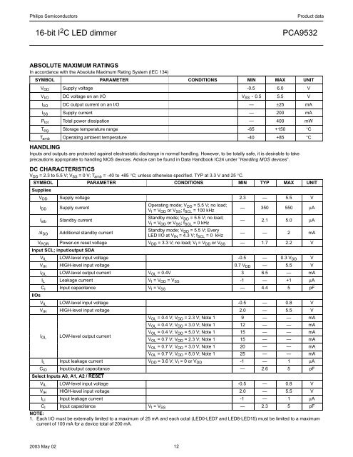
Philips Semiconductors<strong>16</strong>-<strong>bit</strong> I 2 C <strong>LED</strong> <strong>dimmer</strong>Product data<strong>PCA9532</strong>ABSOLUTE MAXIMUM RATINGSIn accordance with the Absolute Maximum Rating System (IEC 134)SYMBOL PARAMETER CONDITIONS MIN MAX UNITV DD Supply voltage -0.5 6.0 VV I/O DC voltage on an I/O V SS - 0.5 5.5 VI I/O DC output current on an I/O — ±25 mAI SS Supply current — 200 mAP tot Total power dissipation — 400 mWT stg Storage temperature range -65 +150 °CT amb Operating ambient temperature -40 +85 °CHANDLINGInputs and outputs are protected against electrostatic discharge in normal handling. However, to be totally safe, it is desirable to takeprecautions appropriate to handling MOS devices. Advice can be found in Data Handbook IC24 under ”Handling MOS devices”.DC CHARACTERISTICSV DD = 2.3 to 5.5 V; V SS = 0 V; T amb = -40 to +85 °C; unless otherwise specified. TYP at 3.3 V and 25 °C.SYMBOL PARAMETER CONDITIONS MIN TYP MAX UNITSuppliesV DD Supply voltage 2.3 — 5.5 VI DD Supply currentOperating mode; V DD = 5.5 V; no load;V I = V DD or V SS ; f SCL = 100 kHz— 350 550 µAI stbStandby currentStandby mode; V DD = 5.5 V; no load;V I = V DD or V SS ; f SCL = 0 kHz— 2.1 5.0 µA∆I DD Additional standby currentStandby mode; V DD = 5.5 V; Every<strong>LED</strong> I/O at V IN = 4.3 V; f SCL = 0 kHz— — 2 mAV POR Power-on reset voltage V DD = 3.3 V; no load; V I = V DD or V SS — 1.7 2.2 VInput SCL; input/output SDAV IL LOW-level input voltage -0.5 — 0.3 V DD VV IH HIGH-level input voltage 0.7 V DD — 5.5 VI OL LOW-level output current V OL = 0.4V 3 6.5 — mAI L Leakage current V I = V DD = V SS -1 — +1 µAI/OsC I Input capacitance V I = V SS — 4.4 5 pFV IL LOW-level input voltage -0.5 — 0.8 VV IH HIGH-level input voltage 2.0 — 5.5 VI OLLOW-level output currentV OL = 0.4 V; V DD = 2.3 V; Note 1 9 — — mAV OL = 0.4 V; V DD = 3.0 V; Note 1 12 — — mAV OL = 0.4 V; V DD = 5.0 V; Note 1 15 — — mAV OL = 0.7 V; V DD = 2.3 V; Note 1 15 — — mAV OL = 0.7 V; V DD = 3.0 V; Note 1 20 — — mAV OL = 0.7 V; V DD = 5.0 V; Note 1 25 — — mAI L Input leakage current V DD = 3.6 V; V I = 0 or V DD -1 — 1 µAC IO Input/output capacitance — 2.6 5 pFSelect Inputs A0, A1, A2 / RESETV IL LOW-level input voltage -0.5 — 0.8 VV IH HIGH-level input voltage 2.0 — 5.5 VI LI Input leakage current -1 — 1 µAC I Input capacitance V I = V SS — 2.3 5 pFNOTE:1. Each I/O must be externally limited to a maximum of 25 mA and each octal (<strong>LED</strong>0-<strong>LED</strong>7 and <strong>LED</strong>8-<strong>LED</strong>15) must be limited to a maximumcurrent of 100 mA for a device total of 200 mA.2003 May 02 12