FDG901D Slew Rate Control Driver IC for P-Channel MOSFETs
FDG901D Slew Rate Control Driver IC for P-Channel MOSFETs
FDG901D Slew Rate Control Driver IC for P-Channel MOSFETs

You also want an ePaper? Increase the reach of your titles
YUMPU automatically turns print PDFs into web optimized ePapers that Google loves.
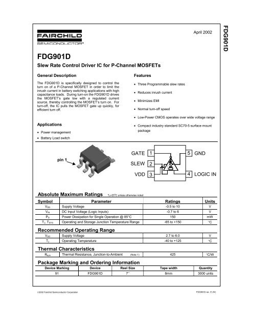
<strong>FDG901D</strong><strong>Slew</strong> <strong>Rate</strong> <strong>Control</strong> <strong>Driver</strong> <strong>IC</strong> <strong>for</strong> P-<strong>Channel</strong> <strong>MOSFETs</strong>April 2002<strong>FDG901D</strong>General DescriptionThe <strong>FDG901D</strong> is specifically designed to control theturn on of a P-<strong>Channel</strong> MOSFET in order to limit theinrush current in battery switching applications with highcapacitance loads. During turn-on the <strong>FDG901D</strong> drivesthe MOSFET’s gate low with a regulated currentsource, thereby controlling the MOSFET’s turn on. Forturn-off, the <strong>IC</strong> pulls the MOSFET gate up quickly, <strong>for</strong>efficient turn off.Features• Three Programmable slew rates• Reduces inrush current• Minimizes EMI• Normal turn-off speed• Low-Power CMOS operates over wide voltage rangeApplications• Power management• Battery Load switch• Compact industry standard SC70-5 surface mountpackageGATE15GNDpin 1SLEW2VDD34LOG<strong>IC</strong> INAbsolute Maximum RatingsTA=25 o C unless otherwise notedSymbol Parameter Ratings UnitsV DD Supply Voltage -0.5 to 10 VV IN DC Input Voltage (Logic Inputs) -0.7 to 6 VP D Power Dissipation <strong>for</strong> Single Operation @ 85°C 150 mWT J, T STG Operating and Storage Junction Temperature Range -65 to +150 °CRecommended Operating RangeV DD Supply Voltage 2.7 to 6.0 VT J Operating Temperature -40 to +125 °CThermal CharacteristicsR θJA Thermal Resistance, Junction-to-Ambient (Note 1) 425 °C/WPackage Marking and Ordering In<strong>for</strong>mationDevice Marking Device Reel Size Tape width Quantity91 <strong>FDG901D</strong> 7’’ 8mm 3000 units©2002 Fairchild Semiconductor Corporation <strong>FDG901D</strong> rev. E (W)
Electrical CharacteristicsT A= 25°C unless otherwise notedSymbol Parameter Test Conditions Min Typ Max UnitsLogic LevelsV IH Logic HIGH Input Voltage V DD = 2.70V to 6.0 VV IL Logic LOW Input Voltage V DD = 2.70V to 6.0 V75%of V DD25%of V DDOFF CharacteristicsBV IN Logic Input Breakdown Voltage I IN = 10µA, V SLEW = 0 V 9 VBV SLEW <strong>Slew</strong> Input Breakdown Voltage I SLEW = 10µA, V IN = 0 V 9 VBV DG Supply Input Breakdown Voltage I DG = 10µA, V IN = 0 V, V SLEW = 0 V 9 VI RINLOG<strong>IC</strong> Input Leakage Current V IN = 8 V, V SLEW = 0 V 100 nAI RSLEW SLEW Input Leakage Current V SLEW = 8 V, V IN = 0 V 100 nAI RDG Supply Input Leakage Current V DG = 8 V, V IN = 0 V, V SLEW = 0 V 100 nAON CharacteristicsI G Gate Current V IN = 6V SLEW = OPEN 90 120 µAV GATE = 2V SLEW = GND 1 10 µASwitching Characteristicst don Output Turn-On Delay Time<strong>Slew</strong> Pin = OPENt don Output Turn-On Delay Time<strong>Slew</strong> Pin = GROUNDt don Output Turn-On Delay Time<strong>Slew</strong> Pin = VDDt rise Output Rise Time<strong>Slew</strong> Pin = OPENt rise Output Rise Time<strong>Slew</strong> Pin = GROUNDt rise Output Rise Time<strong>Slew</strong> Pin = VDDdv/dt Output <strong>Slew</strong> <strong>Rate</strong><strong>Slew</strong> Pin = OPENdv/dt Output <strong>Slew</strong> <strong>Rate</strong><strong>Slew</strong> Pin = GROUNDdv/dt Output <strong>Slew</strong> <strong>Rate</strong><strong>Slew</strong> Pin = VDDV Supply = 5.5 V, V DD = 5.5 V,Logic IN = 5.5 V,C LOAD = 510 pF, Test CircuitV Supply = 5.5 V, V DD = 5.5 V,Logic IN = 5.5 V,C LOAD = 510 pF, Test CircuitV Supply = 5.5 V, V DD = 5.5 V,Logic IN = 5.5 V,C LOAD = 510 pF, Test CircuitSLEW = V DD 10 50 nAVV8.3 µs0.6 ms2.2 ms28 µs1.8 ms11 ms162 V/ms2.6 V/ms0.3 V/ms<strong>FDG901D</strong>Notes: R θJAis the sum of the junction-to-case and case-to-ambient thermal resistance where the case thermal reference is defined as the solder mounting surfaceof the drain pins. R θJCis guaranteed by design while R θCAis determined by the user's board design.VDDV SUPPLY C LoadSLEW23LOG<strong>IC</strong> IN10%190%LOG<strong>IC</strong> IN45OUTPUT(Inverted)10%tdonTest CircuittriseSwitching Wave<strong>for</strong>ms<strong>FDG901D</strong> rev. D (W)
Typical Characteristics10095<strong>Slew</strong> = OpenVdd=Vin=6V2.0<strong>Slew</strong> = GndVdd=Vin=6V<strong>FDG901D</strong>901.5Gate Current, (µA)858075Gate Current (µA)1.0700.56560-50 0 50 100 150Temperature, ( o C)0.0-50 0 50 100 150Temperature, ( o C)Figure 1. GATE Output current vs.Temperature. SLEW = OPENFigure 2. GATE Output current vs.Temperature. SLEW = GroundGate Current, (nA)14121086<strong>Slew</strong> = VddVdd=Vin=6VOutput Risetime, microseconds (µsec)100101<strong>Slew</strong> = OpenVdd=Vin=5.5V4-50 0 50 100 150Temperature, ( o C)0.11 10 100 1000Load Capacitance, picoFarad (pF)Figure 3. GATE Output current vs.Temperature. SLEW = V DDFigure 4. t rise vs. Load Capacitance.SLEW = OPENOutput Risetime, microseconds (µs)10000100010010<strong>Slew</strong> = GndVdd=Vin=5.5VOutput Risetime, milliseconds (ms)100101<strong>Slew</strong> = VddVdd=Vin=5.5V11 10 100 1000Load Capacitance, picoFarad (pF)0.11 10 100 1000Load Capacitance, picoFarad (pF)Figure 5. t rise vs. Load Capacitance.SLEW = GROUNDFigure 6. t rise vs. Load Capacitance.SLEW = V DD<strong>FDG901D</strong> rev. D (W)
ISourceDrainGateLoadLogicSignal<strong>Slew</strong> <strong>Rate</strong><strong>Control</strong>42VDD351IgApplication CircuitTypical ApplicationBattery powered systems make extensive usage of load switching, turning the power tosubsystems off, in order to extend battery life. Power <strong>MOSFETs</strong> are used to accomplish thistask. In PDA’s and Cell phones, these <strong>MOSFETs</strong> are usually low threshold P-<strong>Channel</strong>s. Sincethe loads typically include bypass capacitor components (high capacitive component), a highinrush current can occur when the load is switched on. This inrush current can cause transientson the main power supply disturbing circuitry supplied by it.The simplest method of limiting the inrush current is to control the slew rate of the <strong>MOSFETs</strong>witch. This can be done with external R/C circuits, but this approach can occupy significant PCBarea, and involves other compromises in per<strong>for</strong>mance. The slew rate control driver <strong>IC</strong> <strong>FDG901D</strong>is specifically designed to interface low voltage digital circuitry with power <strong>MOSFETs</strong> and reducethe rapid inrush current in load switch applications. The <strong>IC</strong> limits inrush current by controlling thecurrent, which drives the gate of the P-<strong>Channel</strong> MOSFET switch.The control input is a CMOS compatible input with a minimum high input voltage of 2.55V with apower rail voltage of 6V. There<strong>for</strong>e, it is compatible with any CMOS logic voltages between2.55V and 5V and under these conditions there is no additional configuration required.<strong>FDG901D</strong> rev. D (W)
The <strong>Slew</strong> <strong>Rate</strong> <strong>Control</strong> <strong>Driver</strong> (<strong>FDG901D</strong>) is designed to give a programmed choice of one ofthree steady dv/dt states on the output during turn-on. To change the dv/dt value, the user needsto use the <strong>Slew</strong> <strong>Rate</strong> <strong>Control</strong> Pin (Pin 2). To utilize the smallest current setting (≈10 nA) from the<strong>IC</strong>, a voltage equal to Vdd must be applied to the <strong>Slew</strong> <strong>Rate</strong> <strong>Control</strong> Pin 2. To use the nexthigher current setting (≈1 µA) a voltage equal to Ground must be applied to Pin 2. To achieve thehighest current setting (≈ 80 µA) or obtain a faster switching speed, the <strong>Slew</strong> <strong>Rate</strong> Pin2 must beopen (floating). A higher value of capacitance will result in a slower switching rate. To determinethe switching times of each setting use the simple equation:Qt =Iwhere Q g is the Gate charge in nC <strong>for</strong> a given MOSFET and I G is the gate current controlled bythe slew rate pin.Below is a captured image from an oscilloscope depicting the device response. The <strong>FDG901D</strong>was connected to control an FDG258P P-<strong>Channel</strong> DMOS. The <strong>Slew</strong> <strong>Rate</strong> control pin was set toopen (floating state).gGTest Conditions:V DD = 5.5VV IN = 5.5VR LOAD = 1.5ΩV INV gate (inverted)V RLoadCircuit wave<strong>for</strong>ms <strong>for</strong> an <strong>FDG901D</strong> controlling a P-<strong>Channel</strong> FDG258P MOSFET.<strong>FDG901D</strong> rev. D (W)
TRADEMARKSThe following are registered and unregistered trademarks Fairchild Semiconductor owns or is authorized to use and isnot intended to be an exhaustive list of all such trademarksACExBottomlessCoolFETCROSSVOLTDenseTrenchDOMEEcoSPARKE 2 CMOS TMEnSigna TMFACTFACT Quiet SeriesSTAR*POWER is used under licenseDISCLAIMERFAIRCHILD SEM<strong>IC</strong>ONDUCTOR RESERVES THE RIGHT TO MAKE CHANGES WITHOUT FURTHERNOT<strong>IC</strong>E TO ANY PRODUCTS HEREIN TO IMPROVE RELIABILITY, FUNCTION OR DESIGN FAIRCHILDDOES NOT ASSUME ANY LIABILITY ARISING OUT OF THE APPL<strong>IC</strong>ATION OR USE OF ANY PRODUCTOR CIRCUIT DESCRIBED HEREIN; NEITHER DOES IT CONVEY ANY L<strong>IC</strong>ENSE UNDER ITS PATENTRIGHTS, NOR THE RIGHTS OF OTHERSLIFE SUPPORT POL<strong>IC</strong>YFAIRCHILD’S PRODUCTS ARE NOT AUTHORIZED FOR USE AS CRIT<strong>IC</strong>AL COMPONENTS IN LIFE SUPPORTDEV<strong>IC</strong>ES OR SYSTEMS WITHOUT THE EXPRESS WRITTEN APPROVAL OF FAIRCHILD SEM<strong>IC</strong>ONDUCTOR CORPORATIONAs used herein:1 Life support devices or systems are devices orsystems which, (a) are intended <strong>for</strong> surgical implant intothe body, or (b) support or sustain life, or (c) whosefailure to per<strong>for</strong>m when properly used in accordancewith instructions <strong>for</strong> use provided in the labeling, can bereasonably expected to result in significant injury to theuserPRODUCT STATUS DEFINITIONSDefinition of TermsFAST âFASTrFRFETGlobalOptoisolatorGTOHiSeCI 2 CISOPLANARLittleFETMicroFETMicroPakM<strong>IC</strong>ROWIREOPTOLOG<strong>IC</strong> âOPTOPLANARPACMANPOPPower247PowerTrenchQFETQS2 A critical component is any component of a lifesupport device or system whose failure to per<strong>for</strong>m canbe reasonably expected to cause the failure of the lifesupport device or system, or to affect its safety oreffectivenessDatasheet Identification Product Status DefinitionâQT OptoelectronicsQuiet SeriesSILENT SWITCHER âSMART STARTSPMSTAR*POWERStealthSuperSOT-3SuperSOT-6SuperSOT-8SyncFETTinyLogicTruTranslationUHCUltraFET âVCXAdvance In<strong>for</strong>mationPreliminaryNo Identification NeededFormative orIn DesignFirst ProductionFull ProductionThis datasheet contains the design specifications <strong>for</strong>product development Specifications may change inany manner without noticeThis datasheet contains preliminary data, andsupplementary data will be published at a later dateFairchild Semiconductor reserves the right to makechanges at any time without notice in order to improvedesignThis datasheet contains final specifications FairchildSemiconductor reserves the right to make changes atany time without notice in order to improve designObsoleteNot In ProductionThis datasheet contains specifications on a productthat has been discontinued by Fairchild semiconductorThe datasheet is printed <strong>for</strong> reference in<strong>for</strong>mation onlyRev H5