AN 1128 L Band Amplifier Using the ATF-36077 Low Noise PHEMT
AN 1128 L Band Amplifier Using the ATF-36077 Low Noise PHEMT
AN 1128 L Band Amplifier Using the ATF-36077 Low Noise PHEMT
- No tags were found...

You also want an ePaper? Increase the reach of your titles
YUMPU automatically turns print PDFs into web optimized ePapers that Google loves.
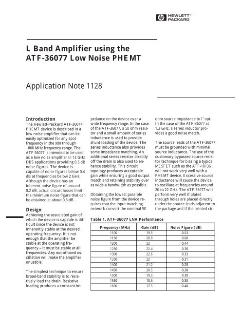
L <strong>Band</strong> <strong>Amplifier</strong> using <strong>the</strong><strong>ATF</strong>-<strong>36077</strong> <strong>Low</strong> <strong>Noise</strong> <strong>PHEMT</strong>Application Note <strong>1128</strong>IntroductionThe Hewlett-Packard <strong>ATF</strong>-<strong>36077</strong><strong>PHEMT</strong> device is described in alow noise amplifier that can beeasily optimized for any spotfrequency in <strong>the</strong> 900 through1800 MHz frequency range. The<strong>ATF</strong>-<strong>36077</strong> is intended to be usedas a low noise amplifier in 12 GHzDBS applications providing 0.5 dBnoise figures. The device iscapable of noise figures below 0.4dB at frequencies below 2 GHz.Although <strong>the</strong> device has aninherent noise figure of around0.2 dB, actual circuit losses limit<strong>the</strong> minimum noise figure that canbe obtained at about 0.3 dB.DesignAchieving <strong>the</strong> associated gain ofwhich <strong>the</strong> device is capable is difficultsince <strong>the</strong> device is notinherently stable at <strong>the</strong> desiredoperating frequency. It is notenough that <strong>the</strong> amplifier bestable at <strong>the</strong> operating frequency– it must be stable at allfrequencies. Any out-of-band oscillationwill make <strong>the</strong> amplifierunusable.The simplest technique to ensurebroad-band stability is to resistivelyload <strong>the</strong> drain. Resistiveloading produces a constant impedanceon <strong>the</strong> device over awide frequency range. In <strong>the</strong> caseof <strong>the</strong> <strong>ATF</strong>-<strong>36077</strong>, a 50 ohm resistorand a small amount of seriesinductance is used to provideshunt loading of <strong>the</strong> device. Theseries inductance also providessome impedance matching. Anadditional series resistor directlyoff <strong>the</strong> drain is also used to enhancestability. This circuittopology produces acceptablegain while ensuring a good outputmatch and retaining stability overas wide a bandwidth as possible.Obtaining <strong>the</strong> lowest possiblenoise figure from <strong>the</strong> device requiresthat <strong>the</strong> input matchingnetwork convert <strong>the</strong> nominal 50Table 1. <strong>ATF</strong>-<strong>36077</strong> LNA Performanceohm source impedance to Γ opt.In <strong>the</strong> case of <strong>the</strong> <strong>ATF</strong>-<strong>36077</strong> at1.3 GHz, a series inductor providesa good noise match.The source leads of <strong>the</strong> <strong>ATF</strong>-<strong>36077</strong>must be grounded with minimalsource inductance. The use of <strong>the</strong>customary bypassed source resistortechnique for biasing a typicalMESFET such as <strong>the</strong> <strong>ATF</strong>-10136will not work very well with a<strong>PHEMT</strong> device. Excessive sourceinductance will cause <strong>the</strong> deviceto oscillate at frequencies around20 to 22 GHz. The <strong>ATF</strong>-<strong>36077</strong> willperform very well if platedthrough holes are placed directlyunder <strong>the</strong> source leads adjacent to<strong>the</strong> package and if <strong>the</strong> printed cir-Frequency (MHz) Gain (dB) <strong>Noise</strong> Figure (dB)1100 19.5 0.531150 20.8 0.601200 22 0.441250 22.4 0.381300 22.6 0.331350 22 0.311400 21.2 0.281450 20.5 0.281500 19.5 0.301550 18.6 0.301600 17.5 0.40
2cuit board thickness is kept at0.031 inch or less.A schematic diagram and partslist are shown in Figure 1. Theschematic diagram suggests <strong>the</strong>use of active biasing to preset <strong>the</strong>bias point. The device is biased ata nominal Vds of 1.5 Volts and anIds of 10 mA. Its operation will beexplained in <strong>the</strong> next section.INPUTZoC1C4L2R5R1ZoR7Figure 1. Schematic and Parts List for <strong>ATF</strong>-<strong>36077</strong> LNAR6L1Q2Z1R8Passive biasing can be used but itwill require that a potentiometerbe connected to <strong>the</strong> output of <strong>the</strong>dc to dc converter U1 to set <strong>the</strong>gate voltage bias required fornominal drain current.PerformanceThe performance of <strong>the</strong> amplifieris shown in Table 1. Since <strong>the</strong> lossof <strong>the</strong> input microstripline canLL1/2Q1 R10 C2 OUTPUTC1 = 22 pF CHIP CAPACITOR C10C2 = 100 pF CHIP CAPACITORC11C3 = NOT USEDC4, C7 = 1000 pF CHIP CAPACITORC5, C6 = NOT USED, GROUND SOURCES DIRECTLYC9 = NOT USEDC8, C12, C13 = 0.1 µF CHIP CAPACITORC10, C11 = 10 µF CHIP CAPACITORL1 = 6T 0.007" DIA. WIRE, 0.050" ID, 0.14" LENGTHL2 = 0.18 TO 0.33 µH RFCLL1, LL2 = PLATED THROUGH HOLES TO BACKSIDE GROUNDPL<strong>AN</strong>E DIRECTLY UNDER EACH LEADQ1 = HEWLETT-PACKARD <strong>ATF</strong>-<strong>36077</strong> <strong>PHEMT</strong>R1 = 100 OHM CHIP RESISTORR2 = NOT USEDR3 = 50 OHM CHIP RESISTORR4 = NOT USEDR5, R7 = 10 k OHM CHIP RESISTORR6 = 1.3 k OHM CHIP RESISTORR8 = 2.7 k OHM CHIP RESISTOR (SETS DRAIN VOLTAGE)R9 = 270 OHM CHIP RESISTOR (SETS DRAIN CURRENT)R10 = 16 OHM CHIP RESISTOR (UP TO 27 OHMS OK)U1 = LINEAR TECHNOLOGY LTC1044CS8 VOLTAGE CONVERTERU2 = 5 VOLT REGULATOR TOKO TK11650UU3 = OPTIONAL MMIC AMP - NOT USEDZo = 50 OHM MICROSTRIPLINE, MINIMIZE LENGTH ON INPUT TO MINIMIZE LOSS <strong>AN</strong>D EFFECTON NOISE FIGUREU1R9C7C12R3L23 VC8U2ZoC13V DDadd appreciable loss which addsdirectly to noise figure, <strong>the</strong>breadboard amplifier was builtwithout any significant microstripetch in <strong>the</strong> input network. Theoptimum noise figure is about0.3 dB and this occurs over abouta 100 MHz bandwidth, centered at1400 MHz. The noise figure risesto 0.4 dB at 1600 MHz and 0.44 dBat 1200 MHz making <strong>the</strong> amplifierusable for broadband GPSapplications. The amplifier can betuned for o<strong>the</strong>r frequencies in <strong>the</strong>900 through 1800 MHz frequencyrange by ei<strong>the</strong>r increasing ordecreasing <strong>the</strong> value of inductorL1.BiasingThe preferred method of biasingFETs is <strong>the</strong> use of an active biasnetwork as described in Figure 1.Although active biasing does addcost by requiring extra components,including a way ofgenerating a negative voltage, <strong>the</strong>advantages generally outweigh <strong>the</strong>disadvantages. Active biasing offers<strong>the</strong> advantage that variationsin pinchoff voltage and Idss willnot necessitate a change in ei<strong>the</strong>r<strong>the</strong> source or drain resistor valuefor a given bias condition. The activebias network automaticallysets Vgs for <strong>the</strong> desired drain current.The typical active biasing schemefor FETs requires that <strong>the</strong> sourceleads be grounded and an additionalsupply be used to generate<strong>the</strong> negative voltage required at<strong>the</strong> gate for typical operation. Referringto Figure 1, resistors R6and R8 provide a regulated voltageat <strong>the</strong> base of Q2. The voltageis increased by 0.7 volts by virtueof <strong>the</strong> emitter-base junction of Q2and <strong>the</strong>n applied to <strong>the</strong> drain ofQ1. Since R3 and R10 are in serieswith <strong>the</strong> drain, <strong>the</strong> voltage drop
<strong>the</strong>n <strong>the</strong> problem may be excessivesource inductance which iscausing a high frequency oscillation.If a device is oscillating atany frequency, even an out of <strong>the</strong>band frequency, it may be difficultto obtain rated performance.Make sure <strong>the</strong> plated throughholes are as close to <strong>the</strong> device aspossible, i.e., 0.02 to 0.03 inch maybe too long.If <strong>the</strong> problem is inband stability,<strong>the</strong>n <strong>the</strong> solution is to add seriesresistance between <strong>the</strong> drain andoutput connector. Increase <strong>the</strong>value of R10. Additional gain reductioncan also be had bydecreasing <strong>the</strong> length of <strong>the</strong> shuntoutput inductor in series with R3.In some cases, higher than expectednoise figure can beattributed to noise from <strong>the</strong> dc todc converter or <strong>the</strong> PNP transistorused for active biasing. Use of a0.1 µF bypass capacitor in parallelwith C4 and at location C8 shouldhelp.The use of a lossy or low Q RFchoke for L2 can contribute to anincrease in noise figure. The useof a small molded RF choke for L2works well in prototypes. For surfacemount applications be sureto choose a high Q wire woundchoke such as those made byCoilCraft.In some instances, <strong>the</strong> enclosurecan cause undesirable feedbackacross <strong>the</strong> circuit board whichcan cause instabilities. This phenomenais true of any amplifierdesign. A cross sectional view of<strong>the</strong> housing can be viewed as apiece of waveguide whose dimensions,both width and height,determine <strong>the</strong> band of frequenciesthat it may pass with minimal attenuation.A combination of <strong>the</strong>amplifier response along with <strong>the</strong>housing response could contributeto instabilities if notcontrolled. The use of low profilesurface mount components willminimize this effect.Making sure that <strong>the</strong> cover is nocloser to <strong>the</strong> printed circuit boardthan is necessary will minimizecoupling from <strong>the</strong> cover. It is preferredto have <strong>the</strong> cover at least0.3 to 0.5 inches above <strong>the</strong> circuitboard. The use of ECOSORBTMcan be used on <strong>the</strong> cover to minimizereflections if <strong>the</strong> cover hasto be in close proximity to <strong>the</strong>board. The use of a metal dividerhanging down from <strong>the</strong> cover isalso ano<strong>the</strong>r method of breakingup enclosure effects.ConclusionThe <strong>ATF</strong>-<strong>36077</strong> can provide lessthan 0.4 dB noise figures over severalhundred MHz of bandwidth atL <strong>Band</strong> frequencies. A simple circuithas been shown that providesstable L <strong>Band</strong> operation.The single-element input matchingnetwork provides very goodperformance in this frequencyrange and offers <strong>the</strong> greatestbandwidth and least sensitivityto manufacturing tolerances. Theresistive loading in <strong>the</strong> outputnetwork provides <strong>the</strong> best broadbandstable performance bysacrificing some in-band gain.For technical assistance or <strong>the</strong> location ofyour nearest Hewlett-Packard sales office,distributor or representative call:Americas/Canada: 1-800-235-0312 or(408) 654-8675Far East/Australasia: Call your local HPsales office.Japan: (81 3) 3335-8152Europe: Call your local HP sales office.Data Subject to ChangeCopyright © 1997 Hewlett-Packard Co.Printed in U.S.A. 5966-0783E (11/97)