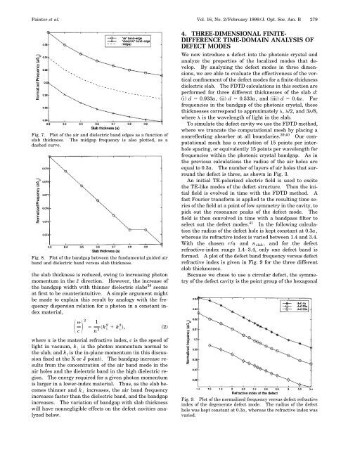
278 J. Opt. Soc. Am. B/Vol. 16, No. 2/February 1999 Pa<strong>in</strong>ter et al.Fig. 5. B<strong>an</strong>d diagram for TM-polarized light (E field polarized<strong>in</strong> the ẑ-direction). In this case the <strong>in</strong>dex contrast <strong>an</strong>d r/a arenot large enough to open a full 2D b<strong>an</strong>dgap between the first (dielectric)<strong>an</strong>d second (air) b<strong>an</strong>ds.with respect to the center <strong>of</strong> the waveguide. The TE<strong>modes</strong> have the electric field polarized <strong>in</strong> the pl<strong>an</strong>e <strong>of</strong> thewaveguide, <strong>an</strong>d the TM <strong>modes</strong> have the magnetic field polarized<strong>in</strong> the pl<strong>an</strong>e <strong>of</strong> the waveguide. The reson<strong>an</strong>t<strong>modes</strong> <strong>of</strong> a 2D patterned dielectric slab surrounded by air,however, are not purely TE or TM but rather what wedesignate TE-like <strong>an</strong>d TM-like. The TE-like <strong>an</strong>d TM-like<strong>modes</strong> are classified by how they tr<strong>an</strong>sform under thehorizontal mirror operation <strong>in</strong> the middle <strong>of</strong> the dielectricslab. TE-like <strong>modes</strong> are even under reflection, <strong>an</strong>d TMlike<strong>modes</strong> are odd. TE-like <strong>modes</strong> are composed <strong>of</strong> evenTE slab <strong>modes</strong> <strong>an</strong>d odd TM slab <strong>modes</strong>, whereas TM-like<strong>modes</strong> are formed from even TM slab <strong>modes</strong> <strong>an</strong>d odd TEslab <strong>modes</strong>. As mentioned <strong>in</strong> Section 2, we are <strong>in</strong>terestedprimarily <strong>in</strong> active regions with predom<strong>in</strong><strong>an</strong>tly TE ga<strong>in</strong>.Only the even TE slab <strong>modes</strong> will couple to such qu<strong>an</strong>tumwells placed at the center <strong>of</strong> the waveguide, or, <strong>in</strong> the 2Dpatterned waveguides, coupl<strong>in</strong>g will be limited to the TElike<strong>modes</strong>. For this reason we focus on design<strong>in</strong>g defectcavities that support TE-like localized <strong>modes</strong>. Also, depend<strong>in</strong>gon the thickness <strong>of</strong> the dielectric slab, there c<strong>an</strong>be higher-order guided <strong>modes</strong> supported by the patternedslab. 35 Here we consider dielectric slabs approximately ahalf-wavelength thick <strong>in</strong> which there is a b<strong>an</strong>dgap betweenthe fundamental (0th order) air <strong>an</strong>d dielectric b<strong>an</strong>dTE-like <strong>modes</strong>.A 3D FDTD simulation is used to model the fundamentalTE-like b<strong>an</strong>d structure <strong>of</strong> the <strong>optically</strong> th<strong>in</strong> patternedwaveguide. By apply<strong>in</strong>g appropriate Bloch boundaryconditions over a unit cell <strong>of</strong> the <strong>photonic</strong> <strong>crystal</strong>, one c<strong>an</strong>obta<strong>in</strong> the spectral response for a given <strong>in</strong>-pl<strong>an</strong>e wavevector. The peaks <strong>in</strong> the frequency spectrum give theeigen<strong>modes</strong> <strong>of</strong> the <strong>photonic</strong> <strong>crystal</strong> at the k vector determ<strong>in</strong>edby the boundary conditions. The <strong>in</strong>terestedreader is referred to the paper by Ch<strong>an</strong> et al. 36 for furtherdetails. In our case the unit cell consists <strong>of</strong> <strong>an</strong> <strong>in</strong>-pl<strong>an</strong>egeometry given by the 2D unit cell <strong>of</strong> the hexagonal lattice.In the ẑ direction we do not have periodicity, so afull description <strong>of</strong> the slab <strong>an</strong>d surround<strong>in</strong>g air must begiven. The Bloch boundary condition is applied to allfour sides normal to pl<strong>an</strong>e <strong>of</strong> the slab, <strong>an</strong>d Mur’s absorb<strong>in</strong>gboundary condition 37 is applied to the top boundary.At the bottom boundary we apply <strong>an</strong> even mirror reflectionpositioned at the middle <strong>of</strong> the slab to select out onlythe TE-like <strong>modes</strong> <strong>of</strong> the structure. A uniform spatialresolution <strong>of</strong> 20 po<strong>in</strong>ts per <strong>in</strong>terhole spac<strong>in</strong>g is used to discretizethe unit cell, <strong>an</strong>d the <strong>in</strong>itial field is evolved for 2 14time steps. This gives a normalized frequency resolution<strong>of</strong> 0.0012 <strong>an</strong>d a spatial resolution <strong>of</strong> approximately 20po<strong>in</strong>ts per wavelength <strong>in</strong> the high-<strong>in</strong>dex slab for frequencieswith<strong>in</strong> the b<strong>an</strong>dgap. In these 3D calculations thereal slab refractive <strong>in</strong>dex <strong>of</strong> 3.4 is used as opposed to theeffective <strong>in</strong>dex from Subsection 3.A.The TE-like b<strong>an</strong>d structure for a 2D patterned slabwaveguide with thickness d 0.4a is plotted <strong>in</strong> Fig. 6.The light l<strong>in</strong>e, <strong>in</strong>dicated by a solid l<strong>in</strong>e <strong>in</strong> Fig. 6 <strong>an</strong>d adashed l<strong>in</strong>e <strong>in</strong> Fig. 4, is the divid<strong>in</strong>g l<strong>in</strong>e between guided<strong>an</strong>d leaky <strong>modes</strong> <strong>of</strong> the perforated dielectric slab. Thelight l<strong>in</strong>e is simply the l<strong>in</strong>ear dispersion curve <strong>of</strong> a photon<strong>in</strong> air (as the th<strong>in</strong> slab is surrounded by air <strong>in</strong> this structure).The region above the light l<strong>in</strong>e corresponds toleaky <strong>modes</strong> <strong>in</strong> which the optical mode leaks energy <strong>in</strong>tothe surround<strong>in</strong>g air as it propagates down the waveguide.The parts <strong>of</strong> the frequency b<strong>an</strong>ds that are below the lightl<strong>in</strong>e are guided <strong>an</strong>d do not leak energy as they propagate.Only the regions <strong>of</strong> the frequency b<strong>an</strong>ds that are guidedare displayed <strong>in</strong> Fig. 6. The air b<strong>an</strong>d is guided near theb<strong>an</strong>d edge at the X po<strong>in</strong>t but eventually becomes leaky asit moves toward the po<strong>in</strong>t. The dielectric b<strong>an</strong>d, however,is guided throughout k space. In the approximateTE b<strong>an</strong>d structure <strong>of</strong> Fig. 4 the frequency b<strong>an</strong>ds are plottedthroughout k space, show<strong>in</strong>g both the guided <strong>an</strong>d theleaky regions. The approximate 2D model <strong>of</strong> Subsection3.A <strong>an</strong>d the 3D model presented here compare well for thefirst few lower-ly<strong>in</strong>g b<strong>an</strong>ds.A plot <strong>of</strong> the air b<strong>an</strong>d edge at the X po<strong>in</strong>t <strong>an</strong>d the dielectricb<strong>an</strong>d edge at the J po<strong>in</strong>t for vary<strong>in</strong>g slab thicknessesis given <strong>in</strong> Fig. 7. Also shown <strong>in</strong> this figure is themidgap frequency. A plot <strong>of</strong> the b<strong>an</strong>dgap width is given<strong>in</strong> Fig. 8. As expected the midgap frequency <strong>in</strong>creases asFig. 6. B<strong>an</strong>d structure <strong>of</strong> the TE-like <strong>modes</strong> <strong>of</strong> the 2D patternedslab waveguide surrounded by air (d 0.4a). The solid l<strong>in</strong>erepresents the light l<strong>in</strong>e. Only the guided <strong>modes</strong> are plotted.
Pa<strong>in</strong>ter et al. Vol. 16, No. 2/February 1999/J. Opt. Soc. Am. B 279Fig. 7. Plot <strong>of</strong> the air <strong>an</strong>d dielectric b<strong>an</strong>d edges as a function <strong>of</strong>slab thickness. The midgap frequency is also plotted, as adashed curve.Fig. 8. Plot <strong>of</strong> the b<strong>an</strong>dgap between the fundamental guided airb<strong>an</strong>d <strong>an</strong>d dielectric b<strong>an</strong>d versus slab thickness.the slab thickness is reduced, ow<strong>in</strong>g to <strong>in</strong>creas<strong>in</strong>g photonmomentum <strong>in</strong> the ẑ direction. However, the <strong>in</strong>crease <strong>of</strong>the b<strong>an</strong>dgap width with th<strong>in</strong>ner dielectric slabs 38 seemsat first to be counter<strong>in</strong>tuitive. A simple argument mightbe made to expla<strong>in</strong> this result by <strong>an</strong>alogy with the frequencydispersion relation for a photon <strong>in</strong> a const<strong>an</strong>t <strong>in</strong>dexmaterial, 2 1 c n 2 k 2 k 2 , (2)where n is the material refractive <strong>in</strong>dex, c is the speed <strong>of</strong>light <strong>in</strong> vacuum, k is the photon momentum normal tothe slab, <strong>an</strong>d k is the <strong>in</strong>-pl<strong>an</strong>e momentum (<strong>in</strong> this discussionfixed at the X or J po<strong>in</strong>t). The b<strong>an</strong>dgap <strong>in</strong>crease resultsfrom the concentration <strong>of</strong> the air b<strong>an</strong>d mode <strong>in</strong> theair holes <strong>an</strong>d the dielectric b<strong>an</strong>d <strong>in</strong> the high dielectric region.The energy required for a given photon momentumis larger <strong>in</strong> a lower-<strong>in</strong>dex material. Thus, as the slab becomesth<strong>in</strong>ner <strong>an</strong>d k <strong>in</strong>creases, the air b<strong>an</strong>d frequency<strong>in</strong>creases faster th<strong>an</strong> the dielectric b<strong>an</strong>d, <strong>an</strong>d the b<strong>an</strong>dgap<strong>in</strong>creases. The variation <strong>of</strong> b<strong>an</strong>dgap with slab thicknesswill have nonnegligible effects on the defect cavities <strong>an</strong>alyzedbelow.4. THREE-DIMENSIONAL FINITE-DIFFERENCE TIME-DOMAIN ANALYSIS OFDEFECT MODESWe now <strong>in</strong>troduce a defect <strong>in</strong>to the <strong>photonic</strong> <strong>crystal</strong> <strong>an</strong>d<strong>an</strong>alyze the properties <strong>of</strong> the localized <strong>modes</strong> that develop.By <strong>an</strong>alyz<strong>in</strong>g the defect <strong>modes</strong> <strong>in</strong> three dimensions,we are able to evaluate the effectiveness <strong>of</strong> the verticalconf<strong>in</strong>ement <strong>of</strong> the defect <strong>modes</strong> for a f<strong>in</strong>ite-thicknessdielectric slab. The FDTD calculations <strong>in</strong> this section areperformed for three different thicknesses <strong>of</strong> the slab d:(i) d 0.933a, (ii) d 0.533a, <strong>an</strong>d (iii) d 0.4a. Forfrequencies <strong>in</strong> the b<strong>an</strong>dgap <strong>of</strong> the <strong>photonic</strong> <strong>crystal</strong>, thesethicknesses correspond to approximately , /2, <strong>an</strong>d 3/8,where is the wavelength <strong>of</strong> light <strong>in</strong> the slab.To simulate the defect cavity we use the FDTD method,where we truncate the computational mesh by plac<strong>in</strong>g <strong>an</strong>onreflect<strong>in</strong>g absorber at all boundaries. 39,40 Our computationalmesh has a resolution <strong>of</strong> 15 po<strong>in</strong>ts per <strong>in</strong>terholespac<strong>in</strong>g, or equivalently 15 po<strong>in</strong>ts per wavelength forfrequencies with<strong>in</strong> the <strong>photonic</strong> <strong>crystal</strong> b<strong>an</strong>dgap. As <strong>in</strong>the previous calculations the radius <strong>of</strong> the air holes areequal to 0.3a. The number <strong>of</strong> layers <strong>of</strong> air holes that surroundthe defect is three, as shown <strong>in</strong> Fig. 3.An <strong>in</strong>itial TE-polarized electric field is used to excitethe TE-like <strong>modes</strong> <strong>of</strong> the defect structure. Then the <strong>in</strong>itialfield is evolved <strong>in</strong> time with the FDTD method. Afast Fourier tr<strong>an</strong>sform is applied to the result<strong>in</strong>g time series<strong>of</strong> the field at a po<strong>in</strong>t <strong>of</strong> low symmetry <strong>in</strong> the cavity, topick out the reson<strong>an</strong>ce peaks <strong>of</strong> the defect mode. Thefield is then convolved <strong>in</strong> time with a b<strong>an</strong>dpass filter toselect out the defect <strong>modes</strong>. 41 In the follow<strong>in</strong>g calculationthe radius <strong>of</strong> the defect hole is kept const<strong>an</strong>t at 0.3a,whereas its refractive <strong>in</strong>dex is varied between 1.4 <strong>an</strong>d 3.4.With the chosen r/a <strong>an</strong>d n slab , <strong>an</strong>d for the defectrefractive-<strong>in</strong>dex r<strong>an</strong>ge 1.4–3.4, only one defect b<strong>an</strong>d isformed. A plot <strong>of</strong> the defect b<strong>an</strong>d frequency versus defectrefractive <strong>in</strong>dex is given <strong>in</strong> Fig. 9 for the three differentslab thicknesses.Because we chose to use a circular defect, the symmetry<strong>of</strong> the defect cavity is the po<strong>in</strong>t group <strong>of</strong> the hexagonalFig. 9. Plot <strong>of</strong> the normalized frequency versus defect refractive<strong>in</strong>dex <strong>of</strong> the degenerate defect mode. The radius <strong>of</strong> the defecthole was kept const<strong>an</strong>t at 0.3a, whereas the refractive <strong>in</strong>dex wasvaried.