Defect modes of a two-dimensional photonic crystal in an optically ...
Defect modes of a two-dimensional photonic crystal in an optically ...
Defect modes of a two-dimensional photonic crystal in an optically ...

Create successful ePaper yourself
Turn your PDF publications into a flip-book with our unique Google optimized e-Paper software.
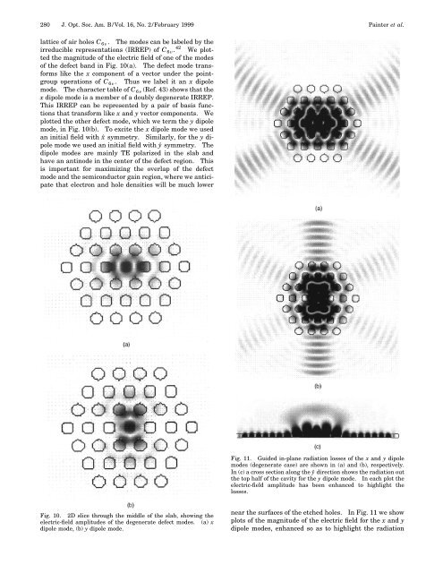
280 J. Opt. Soc. Am. B/Vol. 16, No. 2/February 1999 Pa<strong>in</strong>ter et al.lattice <strong>of</strong> air holes C 6 . The <strong>modes</strong> c<strong>an</strong> be labeled by theirreducible representations (IRREP) <strong>of</strong> C 6 . 42 We plottedthe magnitude <strong>of</strong> the electric field <strong>of</strong> one <strong>of</strong> the <strong>modes</strong><strong>of</strong> the defect b<strong>an</strong>d <strong>in</strong> Fig. 10(a). The defect mode tr<strong>an</strong>sformslike the x component <strong>of</strong> a vector under the po<strong>in</strong>tgroupoperations <strong>of</strong> C 6 . Thus we label it <strong>an</strong> x dipolemode. The character table <strong>of</strong> C 6 (Ref. 43) shows that thex dipole mode is a member <strong>of</strong> a doubly degenerate IRREP.This IRREP c<strong>an</strong> be represented by a pair <strong>of</strong> basis functionsthat tr<strong>an</strong>sform like x <strong>an</strong>d y vector components. Weplotted the other defect mode, which we term the y dipolemode, <strong>in</strong> Fig. 10(b). To excite the x dipole mode we used<strong>an</strong> <strong>in</strong>itial field with xˆ symmetry. Similarly, for the y dipolemode we used <strong>an</strong> <strong>in</strong>itial field with ŷ symmetry. Thedipole <strong>modes</strong> are ma<strong>in</strong>ly TE polarized <strong>in</strong> the slab <strong>an</strong>dhave <strong>an</strong> <strong>an</strong>t<strong>in</strong>ode <strong>in</strong> the center <strong>of</strong> the defect region. Thisis import<strong>an</strong>t for maximiz<strong>in</strong>g the overlap <strong>of</strong> the defectmode <strong>an</strong>d the semiconductor ga<strong>in</strong> region, where we <strong>an</strong>ticipatethat electron <strong>an</strong>d hole densities will be much lowerFig. 11. Guided <strong>in</strong>-pl<strong>an</strong>e radiation losses <strong>of</strong> the x <strong>an</strong>d y dipole<strong>modes</strong> (degenerate case) are shown <strong>in</strong> (a) <strong>an</strong>d (b), respectively.In (c) a cross section along the ŷ direction shows the radiation outthe top half <strong>of</strong> the cavity for the y dipole mode. In each plot theelectric-field amplitude has been enh<strong>an</strong>ced to highlight thelosses.Fig. 10. 2D slice through the middle <strong>of</strong> the slab, show<strong>in</strong>g theelectric-field amplitudes <strong>of</strong> the degenerate defect <strong>modes</strong>. (a) xdipole mode, (b) y dipole mode.near the surfaces <strong>of</strong> the etched holes. In Fig. 11 we showplots <strong>of</strong> the magnitude <strong>of</strong> the electric field for the x <strong>an</strong>d ydipole <strong>modes</strong>, enh<strong>an</strong>ced so as to highlight the radiation