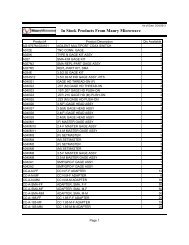
Cascade Microtech - MB Electronique
Cascade Microtech - MB Electronique
Cascade Microtech - MB Electronique
- No tags were found...

Create successful ePaper yourself
Turn your PDF publications into a flip-book with our unique Google optimized e-Paper software.
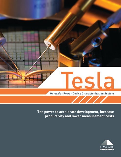
Answering the call for wafer levelpower device characterizationThroughout the world, emerging energy standards are driving a clear and presentdemand for efficient power utilization. In turn, the impact on power semiconductordevice manufacturers is growing. Utilized in industries including transportation,consumer electronics, mobile products, space and medical, efficient powerdevices are in record demand. In fact, market growth for power devices nowexceeds the rest of the semiconductor market. Simply put, the broad use of powerdevices, plus the premium of efficient power utilization, has created enormouspressure for manufacturers to rapidly design, develop and characterize new powerdevices. Time-to-market is everything. And that’s okay, because help is here.Now you have the power to:Reduce overall chip development costIncrease measurement productivityEliminate the cost, delays and uncertaintyof in-package characterizationAccelerate device development for afaster time to marketTesla is the industry’s first complete system for on-wafer power devicecharacterization. By eliminating the need for time-consuming, in-packagecharacterization or risky in-house test solutions, Tesla delivers unprecedentedproductivity gains, faster development cycles and a lower cost of test. Now powerdevice manufacturers can take advantage of a complete on-wafer solution forover temperature, low-contact resistance measurements of power devices upto 60A and 3,000V. Unlike any other commercially available probing system, theTesla system is dedicated exclusively to helping engineers overcome the uniqueon-wafer measurement challenges of power devices. More importantly, Tesla ishere to help power device manufacturers meet and beat the extraordinary pace ofthe global marketplace.The ideal development path —measure, characterize, model and go!<strong>Cascade</strong> <strong>Microtech</strong>’s advanced electrical metrology systems and productionprobes have been cornerstones of the semiconductor development process formore than twenty years. As a result, the broader semiconductor market hasarrived at a streamlined development process that truly helps speed time-torevenue.It’s a process where the device is designed, characterized on-wafer,models are extracted and the device moves quickly to processing for massproduction.Eliminate cumbersome, costly andtime-consuming in-package characterizationThe Tesla system unlocks triaxial measurementsat high voltages so engineers can now uncoverunprecedented levels of device leakage behavior.Until Tesla, power device manufacturers have been straddled with the task ofsending power devices out for packaging prior to characterization and modelextraction. This extra step adds cost, plus development schedules can often facedelays of several weeks or months. By providing accurate, reliable and repeatableon-wafer power device characterization, Tesla erases this unfortunate detourby putting power device characterization on an ideal development path so powerdevice manufacturers can swiftly and cost effectively achieve critical time-tomarketgoals.
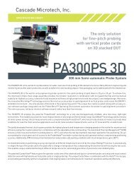
Problems SolvedThe Tesla System has been developed from the ground up to satisfy the unique demands and overcomethe specific challenges associated with achieving accurate, wafer-level power device characterization.Handling thin wafersPROBLEM: With an average thickness of 100µm, today’swafers introduce added complexity to wafer level devicecharacterization. These thin wafers are difficult to holddown on a standard wafer chuck and are often prone tocurling at the ends, much like a potato chip. This createsproblems for wafer probing and, in particular, for securinglow-contact resistance between the wafer and the chuck.SOLUTION: Tesla features a state-of-the-art chuck for handlingfor 3”-to-8” wafers. Innovative VacuChannel technologydelicately provides the appropriate amount of vacuum toprotect against wafer breakage or probe damage. For themost accurate backside connections, a highly polishedgold-top surface ensures low-contact resistance betweenwafer and chuck.High-Current ProbeHigh-Voltage ProbeVacuChannel ChuckT200 Probe StationRds(on) MeasurementsPROBLEM: The pursuit for the ideal power device is leadingengineers to drive the ON state resistance to increasinglylower and lower levels. With today’s power semiconductordevices requiring high-current pulses and VDMOS powerdevices having the drain on the backside, accurate Rds(on)measurements have proven to be more and more difficultand problematic to perform on-wafer.High-current probe burnoutPROBLEM: Accurate probing of power devices requireshigh-current measurement capabilities. Reliablewafer-level characterization of power devices hasalways been a challenge due to inconvenient deviceheating at the probe tip. Furthermore, smaller andsmaller pad dimensions only increase the likelihood ofproblematic device heating at the probe tip.SOLUTION: Tesla enables engineers to make Rds(on)measurements at values lower than ever before on a probestation. This extraordinary performance comes through thehighly polished gold chuck surface and a superior vacuumpattern that provides contact resistance in the milliohm range.Measuring drain resistance at a very high current has neverbeen easier with the HCP probes supporting up to 60A pulses.SOLUTION: Tesla’s high-current probe reduces probe and/ordevice destruction at high currents. It supports 10A DC and upto 60A of pulsed current. By design, the probe tip minimizescontact resistance at the wafer-to-probe interfaceto prevent device heating at the tip. The probe distributescurrent over multiple contact points at the tip and is joined bya single heatsink that pulls pull heat from the probe tip.Low-leakage measurement at high voltagePROBLEM: Precision measurements of high-voltage devicespresent some formidable challenges for probe design.Higher voltage between the force, guard and shield elementsof the probe drives higher leakage currents through theresistance of various isolating materials separating thoseelements. In order to prevent dielectric breakdown (arcing)and maintain a safe operation, the distance must increasebetween internal elements of the probe. Additionally,upgraded cables and connectors are required.SOLUTION: To ensure precision measurements of today’shigh-voltage devices, Tesla’s HVP probes provide increasedisolation resistance and dielectric strength by incorporatingadvanced internal isolation materials, as well as customcabling and connectors. The unique internal design of HVPprobe layers and elements assures the distance achieved byisolating materials, as well as inter-layer creepage paths,will prevent any breakdowns at high voltage and still enablefull triaxial capability.Safety for device, operator and probing equipmentPROBLEM: With power devices requiring upwards of 200V, theintegrity of this high-performance electrical test environmentstarts with ensuring both hardware and humans areprotected from damage and/or severe injury. The advent ofhome-spun device characterization systems can presentseveral safety issues, as these in-house test systems ofteninclude several disparate components and may lack theknow-how to include all required safety protocols.SOLUTION: The entire Tesla system is deliberately designed toensure operator safety while providing a high-performanceelectrical measurement path. Features like an integratedsafety interlock light curtain ensure operator safety duringmeasurements. Additionally, the probe, chuck, chuckenvironment, cables, connectors and interface panelsall contribute to this ultra-safe test environment andhigh-performance electrical path.far left: The Tesla HCP probereduces contact resistance atthe tip through an innovativemulti-finger design thatprovides a distribution ofcurrent for minimal deviceheating at the tip, whileproviding minimal probemarks.left: The Tesla VacuChannelwafer chuck system providesstate-of-the-art handling forthin wafers.
The industry’s first complete systemdedicated to on-wafer power devicecharacterizationBecause Tesla is specifically optimized aroundthe key high-voltage/high-current measurementchallenges unique to power devices, no stone wasleft unturned when designing and developing thiscomplete and comprehensive system. The Teslasystem is engineered to withstand probing levels ofup to 3,000V and 60A; it supports a measurementtemperature range of -55°C to 200°C. Rest assured,Tesla has been built from the ground up to ensurepower device manufacturers will immediatelyreap the benefits of a high-performance electricalmeasurement path in an ultra-safe testingenvironment.The complete Tesla system includesProbe station packageSummit 12000 semiautomatic probe station with low-noise performance package(MicroChamber ® , AttoGuard ® )Thermal wafer chuck packageVacuChannel thermal chuck optimized for minimal chuck-to-wafer contact resistance and thin-wafer mountingHigh-performance thermal controller and chiller systemSafety interlock systemInfrared laser light curtainDeluxe anti-vibration table kitHands-free digital imaging system eVue -II digital imaging system 40X remote focus2X objective with smart objective mountMotorized microscope bridge-mount with 2x2 programmable focusHigh-current probe packageHCP high-current parametric probe holdersBox of five replaceable probe tipsProbe micropositionersHigh-voltage probe packageHVP high-voltage parametric probe holderswith Kelvin sense capabilityBox of 25 replaceable probe tipsProbe micropositionersSystem interface panelsHigh-voltage interface panelHigh-current interface panelCablesHigh-voltage/current cable package© Copyright 2009 <strong>Cascade</strong> <strong>Microtech</strong>, Inc.All rights reserved. <strong>Cascade</strong> <strong>Microtech</strong>, AttoGuard andMicroChamber are registered trademarks and eVue,Summit and VacuChannel are trademarks of <strong>Cascade</strong><strong>Microtech</strong>, Inc. All other trademarks are the property oftheir respective owners.Data subject to change without noticeCorporate Headquarters<strong>Cascade</strong> <strong>Microtech</strong>, Inc.toll free: +1-800-550-3279phone: +1-503-601-1000email: sales@cmicro.com<strong>Cascade</strong> <strong>Microtech</strong> GmbHemail: cmg_sales@cmicro.comphone: +49-811-60005-0<strong>Cascade</strong> <strong>Microtech</strong> Japan, Inc.phone: +81-3-5615-5150email: cmj_sales@cmicro.com<strong>Cascade</strong> <strong>Microtech</strong> Shanghaiphone: +86-21-3330-3188email: cmc_sales@cmicro.com<strong>Cascade</strong> <strong>Microtech</strong> Singaporephone: +65-6873-7482email: cms_sales@cmicro.com<strong>Cascade</strong> <strong>Microtech</strong> Taiwanphone: +886-3-5722810email: cmt_sales@cmicro.comTES-BRO-0809www.cascademicrotech.com