DESIGN AND IMPLEMENTATION OF A PRIVATE AND PUBLIC KEY ...
DESIGN AND IMPLEMENTATION OF A PRIVATE AND PUBLIC KEY ...
DESIGN AND IMPLEMENTATION OF A PRIVATE AND PUBLIC KEY ...

Create successful ePaper yourself
Turn your PDF publications into a flip-book with our unique Google optimized e-Paper software.
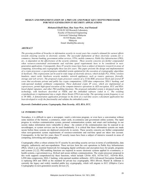
<strong>DESIGN</strong> <strong>AND</strong> <strong>IMPLEMENTATION</strong> <strong>OF</strong> A <strong>PRIVATE</strong> <strong>AND</strong> <strong>PUBLIC</strong> <strong>KEY</strong> CRYPTO PROCESSORFOR NEXT-GENERATION IT SECURITY APPLICATIONSABSTRACTMohamed Khalil Hani, Hau Yuan Wen, Arul PaniandiVLSI-ECAD Research LaboratoryFaculty of Electrical EngineeringUniversiti Teknologi Malaysia81310 Skudai, JohorMalaysiaEmail: khalil@fke.utm.myThe growing problem of breaches in information security in recent years has created a demand for earnest effortstowards ensuring security in electronic systems. The successful deployment of these electronic systems for e-commerce, Internet banking, government online services, VPNs, mobile commerce, Public Key Infrastructure (PKI),etc., is dependent on the effectiveness of the security solutions. These security concerns are further compoundedwhen resource-constrained environments and real-time speed requirements have to be considered in nextgenerationapplications. Consequently, these IT security issues have been a subject of intensive research in areas ofcomputing, networking and cryptography these last few years. This paper presents the design and implementationof a crypto processor, a special-purpose embedded system optimized for the execution of cryptographic algorithmsin hardware. This cryptosystem can be used in wide range of electronic devices, which include PCs, PDAs, wirelesshandsets, smart cards, hardware security modules, network appliances, such as routers, gateways, firewalls,storage and web servers. The proposed crypto processor consists of a 32-bit RISC processor block and several IPcores that accelerates private and public key crypto computations, LZSS data compression, SHA-1 hashing, andwide-operand modular arithmetic computation. These dedicated crypto IP cores, which are implemented ascoprocessors, permit high-speed execution of the compute-intensive operations in AES encryption, ECC and RSAbaseddigital signature, and other PKI-enabling functions. The proposed embedded system is designed using SoCtechnology, with hardware described in VHDL and the embedded software coded in C. The resultingcryptohardware is implemented into a single Altera Stratix FPGA microchip. The operating system frequency is setto 40 MHz. A demonstration application prototype in the form of a real-time secure e-document application hasbeen developed to verify the functionality and validate the embedded system.Keywords: Embedded system, Cryptography, Data Security, AES, RSA, ECC.1.0 INTRODUCTIONNowadays, it is difficult to open a newspaper, watch a television program, or even have a conversation withoutsome mention of the Internet, e-commerce, smart cards, m-commerce and government online systems. The rapidprogress in wireless communication system, personal communication system, and smart card technology in oursociety makes information more vulnerable to abuse - the content of the communication may be exposed to aneavesdropper, or system services can be used fraudulently. It is critical that these information systems are madesecure before these systems are deployed extensively in society. These security concerns are further compoundedwhen next-generation system requirements of resource-constraints and real-time speed are taken into account.Consequently, in the last few years, these IT security issues have been a subject of intensive research in areas ofcomputing, networking and cryptography.Cryptography offers a robust solution for IT security by providing security services in terms of confidentiality, dataintegrity, authenticity and non-repudiation. These services form the core operations in Public Key Infrastructure(PKI), which is an essential framework for managing digital certificates and encryption keys for people, programsand systems [1] [2]. PKI-enabling functions are required in secure electronic systems applied in e-commerce, e-health systems, e-government (e.g. MyKad) and secure military communications. The crypto processor proposed inthis work supports comprehensively these functions, which include 128-bit AES, 163-bit ECC, 1024-bit RSA,LZSS data compression, SHA-1 hashing, wide-operand modular arithmetic. AES (Advanced Encryption Standard)is replacing DES and 3DES as the standard for private key cryptography. RSA (Rivest, Shamir & Adleman iscurrently the legacy and widely installed public key cryptography, which will migrate to ECC (Elliptive CurveCryptography) in next-generation security devices [3].Malaysian Journal of Computer Science, Vol. 19(1), 200629
Design and Implementation of a Private and Public Key Crypto Processor for Next-Generation IT Security Applications pp. 29 - 45Cryptographic (crypto) algorithms can be implemented either in hardware or software. It is relatively easy toimplement crypto algorithms completely in software, but due to increasing data rates and complexity of securityprotocols, such approach is typically too slow for applications such as embedded systems, networks routers, onlinedatabases, etc. These shortcomings are most felt in systems that need to process a large number of transactions atvery high speed (e.g. network routers, firewalls, web servers, online databases), and systems with resourceconstrainedenvironments (e.g. PDAs, cell phones and smart cards). In addition, new techniques for breakingsecurity, such as power analysis and fault analysis, require that the system implementation itself be secure evenwhen it is physical accessed by malicious entities. Resistance to these attacks can be ensured if suitable tamperproofor clone-free features are built in the designs.To achieve optimal system performance while maintaining physical security, it is desirable to implement cryptoalgorithms in hardware. Hardware-based solutions add specific custom crypto hardware components in order tooffload time-consuming computations and to reduce bottleneck. While custom hardware techniques address thesecurity-processing gap to some extent, their implementations are expensive and their flexibility and ability tohandle evolving standards is limited. Hence the emerging trend is to design hardware/software platforms, utilizing acombination of programmable embedded components and hardware for security processing. The solutionimplements only specific parts of the security protocol, that is, the time-consuming crypto algorithms in hardware.This leaves the book-keeping, packet processing, control functionality and other non-computation-intensiveprocessing to be performed by the system’s host processor.Today’s systems, particularly those networked, also need to be flexible if they are to be commercially viable. In thisregard, a desirable feature in most modern security protocol is algorithm agility required to support algorithmindependent protocol. Hence it is desirable to implement crypto algorithms within reconfigurable devices such asField Programmable Gate Arrays (FPGAs). Besides providing for dynamic system evolution, FPGA architecturesalso allow complex arithmetic operations that are not suited to general purpose CPUs to be implemented moreefficiently [4]. They also offer a more cost-effective solution than traditional VLSI/ASIC hardware, which has amuch longer design lead-time. The fast prototyping development time of an FPGA design allows modifications tobe implemented with relative ease [5]. System-on-chip (SoC) design methodology is employed in the hardwaredesign of the proposed cryptosystem. SoC is designed as a programmable platform that integrates most of thefunctions of the end product into a single chip. It incorporates at least one processing element (microprocessor,DSP, etc.) that executes the system embedded software. The SoC system employs a bus-based architecture, whichalso includes peripherals, random logic and interfaces to the outside world. The proposed embedded system isprototyped on an Altera Nios Prototyping Board containing a Stratix EP1S40F780C5 FPGA chip. To the authors’knowledge, the design and single-chip implementation of the combination of the cryptographic algorithms andhybrid systems considered in this paper have not been reported in existing literature.This paper is organized as follows. In Section 2, the hardware architecture of the cryptosystem is presented. This isfollowed by a discussion on an application demonstration prototype of a secure e-document transfer via Internet,provided in Section 3. The design of each crypto co-processor is described in Section 4, which is followed by adiscussion of the FPGA implementation and performance evaluation of the proposed crypto processors. Finally, theconclusion and recommendations for future work are presented in Section 6.2.0 THE EMBEDDED CRYPTOSYSTEM ARCHITECTUREThe block diagram of our embedded cryptosystem is shown in Fig. 1. This single chip cryptosystem has a RS-232UART serial interface logic, on-chip memory, timer, PIO (parallel input/output), bus and interface logic tocommunicate with memory external to the FPGA chip. The crypto co-processors for the ECC, SHA, RSA, AES,LZSS and a modular arithmetic processor are also configured in the same microchip. The proposed cryptoembedded system consists of three main components: (1) Hardware processing blocks, (2) Device Drivers, and (3)Application Programming Interface (API).The Hardware Processing Block consists of a Control CPU and six IP cores (coprocessors) that perform the 128-bitAES symmetric cipher, 1024-bit RSA and 163-bit ECC public key cryptography, SHA-1 algorithm, LZSS datacompression and 163-bit Modular Arithmetic Processing (MAP) unit. The dedicated hardware accelerators result inhigh-speed execution of the crypto algorithms. The embedded control CPU is the Altera Nios processor. Thisprocessor is a configurable, 5-stage pipelined, single-issue RISC processor, in which instructions run in a single30Malaysian Journal of Computer Science, Vol. 19(1), 2006
Design and Implementation of a Private and Public Key Crypto Processor for Next-Generation IT Security Applications pp. 29 - 45clock cycle. It controls the dedicated crypto IP cores such that the embedded system may perform cryptographicschemes such as private key encryption, public key digital signature, mutual authentication, key management, etc.Fig. 1: Block diagram of the proposed crypto embedded systemThe device drivers are embedded software executed on the Nios embedded processor. It is the main controllerensuring the correct execution of the IP cores, and acts as a bridge between the crypto coprocessors and the APIs onthe host PC. The APIs are executed on the host PC. The APIs perform high-level functions such as input filereading and output file writing. It sends data to and receives output between the host PC and the subsystemhardware via a UART serial communication channel. These APIs facilitate software development by applicationdevelopers.For an easier comprehension of the design proposed in this paper, we begin, in the following section, with anoverview of the secure e-document demonstration application prototype implemented in the proposed cryptosystem.In this way, the security schemes implemented are known at the outset, from which the functionality and designs ofthe various crypto co-processors can be explained more conveniently. The designs of these crypto co-processors aredetailed out in Section 4.3.0 APPLICATION: SECURE e-DOCUMENT TRANSFERWe have developed a real-time data security application, that is, an e-document system for the application of securedocument transfer via Internet, which is an insecure communication medium. This demonstration applicationprototype is utilized to evaluate the functionality of the embedded cryptosystem and the reusability of the associatedAPIs and device drivers. In this application, sensitive documents, which are transferred electronically via FTPmechanism in a Local Area Network (LAN) environment, are made secure by encrypting and signing in real-time,using the proposed crypto hardware.Fig. 2 shows GUI of the control and monitoring PC front-end for our e-document security application (written inVisual Basic). There are two processes involved, namely (a) sender file uploading, and (b) receiver file download.The block diagrams for the security schemes at the sender and receiver ends are given in Fig. 3(a) and 3(b)respectively. In the sending process, a document goes through operations depicted in the security scheme given inFig. 3(a), that is:1. PRNG (pseudo random number generation) module generates a session key for AES encryption.2. Using this AES session key, the AES encryptor encrypts the document to produce ciphertext.3. RSA encryptor encrypts AES session key using the receiver RSA public key.4. SHA Hashing module generates a message digest of the document.5. ECDSA signing module computes the corresponding digital signature using sender ECC private key.Malaysian Journal of Computer Science, Vol. 19(1), 200631
Design and Implementation of a Private and Public Key Crypto Processor for Next-Generation IT Security Applications pp. 29 - 45Fig. 2: The GUI of the e-document security systemFig. 3(a): Security scheme for Sender File UploadIn the receiving process, the now secured document undergoes the recovery process depicted in the security schemegiven in Fig. 3(b) to recover the original data, that is:1. ECDSA verifying module verifies the received digital signature, using sender ECC public key. If thissignature verification fails, the receiving process stops here, else continue.2. Using receiver RSA private key, the RSA Decryptor decrypts the encrypted session key to recover the AESsession key.3. With this key, the AES decryptor decrypts ciphertext to recover original document.Fig. 3(b): Security scheme for Receiver File Download32Malaysian Journal of Computer Science, Vol. 19(1), 2006
Design and Implementation of a Private and Public Key Crypto Processor for Next-Generation IT Security Applications pp. 29 - 454.0 THE CRYPTO CO-PROCESSORS4.1 AES Processor for Symmetric EncryptionNIST (National Institute of Standards and Technology, US Government’s official standard organization) has nowspecified AES-Rijndael in the document Federal Information Processing Standard (FIPS) 197, as the new standardfor symmetric encryption. AES comes in three security strengths: 128-bits, 192 bits and 256 bits. In this paper, thearchitecture for 128-bit AES has been designed. The number of rounds depends on both of these parameters and isgiven in [6]. Therefore, the cipher in all configurations presented operates in N r = 10 rounds.(a)(a) Encryption(b) DecryptionFig. 4: Structure of AES algorithmFig. 4 shows the encryption and decryption structure of the AES algorithm applied in this work. In encryption, afterthe initial roundkey addition, N r rounds are performed. The operations are the same in the first N r -1 rounds, with asmall difference in the final round. As shown in Fig. 4(a), each of the first N r -1 rounds consists of fourtransformations: SubBytes, ShiftRows, MixColumns and AddRoundKey. The final round excludes the MixColumnstransformation. The decryption algorithm uses a different ordering of the inverse forms of the transformations usedin the encryption algorithms as shown in Fig. 4(b). The four transformation operations are summarized as follows:• SubBytes: This transformation is a non-linear byte substitution using a substitution table (S-box). The S-box isconstructed of the compositions of two transformations: multiplicative inverse in GF(2 8 ) with irreduciblepolynomial m(x) = x 8 +x 4 +x 3 +x+1, and an affine mapping over GF(2). In the decryption process, the inverse S-box is used.• ShiftRows: In this transformation, the rows of the State shift cyclically to the left with different offsets. In thedecryption process, the shifting offsets have different values.• MixColumns: The MixColumns transformation is performed on the State column-by-column. Each column isconsidered as s four-term polynomial over GF(2 8 ) and multiplier by a(x) modulo x 4 + 1, given by a(x) = {03}x 3+ {01}x 2 + {01}x + 1 for encryption and a(x) = {0B}x 3 + {0D}x 2 + {09}x + {0E} for decryption process.• AddRoundKey: In this transformation, a round key is added to the State using a bitwise Exclusive-OR (XOR)operation. AddRoundKey is the same for the decryption process.The decryption model given in Fig. 4(b) is modified from the original described in the NIST standard. It has beenrearranged with some changes to the key generation unit to obtain a structure similar to the encryption model. Thismodification is based on the properties of the AES algorithm, which is:• InvShiftRows transformation immediately followed by an InvSubBytes transformation is equivalent toInvSubBytes transformation immediately followed by an InvShiftRows transformation.• InvMixColumns transformation is linear, which means:InvMixColumns(State XOR roundkey) = InvMixColumns(State) XOR InvMixColumns(roundkey)Fig. 5 shows the hardware architecture of AES crypto processor core designed in this work. It combines encryptionand decryption into one block, permitting the sharing of common modules. This crypto processor is designed basedMalaysian Journal of Computer Science, Vol. 19(1), 200633
Design and Implementation of a Private and Public Key Crypto Processor for Next-Generation IT Security Applications pp. 29 - 45on 4-state pipeline so as to increase the maximum running frequency and timing performance. It consists of threemain modules, which are KeyGen, Control Unit and Encryption/Decryption Unit. The KeyGen is designed togenerate the roundkey for AddRoundKey transformation in every round. The data path for encryption/decryption isas follows:Pt/Ct → m2 → ARK → M-SB → M-SR → M-MC → m1 → m2 → ARK → Ct/Pt.We implemented the SubBytes block (S-box) based on the calculation of multiplicative inverse and affine transforminstead of using ROM-based lookup table to reduce the hardware logic count.ClkResetM-SB : Mixed SubBytesM-SR : Mixed ShiftRowM-MC : MixedMixColumnARK : AddRoundKeyPt/Ct :Plaintext/CiphertextCt/Pt :Ciphertext/Plaintextm1 : multiplexer 1m2 : multiplexer 2Encryption/DecryptionEncDec datapath M - SBEncDecEncDecPt / CtEncDec128M - SRM - MC128128ARKCt / Pt128m1m2128128Sel_M1KeyBitSel_M2 ReadResultKeyBitRequestLoadDataLoadKeyDoneEncDecKeySelectUpdateKeyKeyRequestDataRequestSel_M1(Final Round)Sel_M2 (First Round)KeyGenClkControlunitResetFig. 5: Block diagram of the AES-128 coreKeykeySelEncDecKeyBit_RequestFirst_RoundFinal_RoundKeyValidDataValidStartEnc4.2 RSA Processor for Public Key CryptographyThe RSA algorithm, invented in 1977 by Rivest, Shamir, and Adleman [7], is currently the most popular public keycryptosystem in use, particularly in high-end commercial software products that are typically employed in e-commerce and VPN servers. It can provide encryption and digital signatures. In hardware implementations, theRSA algorithm can be found in secure telephones, in Ethernet network cards, and smart cards. The main advantageof the algorithm is that it can provide both data confidentiality service (via public-key encryption) and data integrity,authentication and non-repudiation (via digital signatures) using the same key pair and under the same mathematicaloperation. Its hard problem is based on the large integer factorization problem.RSA algorithm is the essence of simplicity [8]. To encrypt a message X to its cipher text P, we perform P = X E modM using the public key (E, M). To restore the message, X= P D mod M is performed, where (D, M) is the private key.For digital signature purpose, we use the private key in signing, S = X D mod M. To verify the signature, we use thepublic key to perform X = S E mod M. Fig. 6 below shows the RSA process. In RSA, whether encrypting,decrypting, signing, or verifying, the operation is basically a wide-operand modular exponentiation. The basicmodular exponentiation equation, given by: Y = X E mod M, essentially consists of thousands of modularmultiplication, A.B mod M, in GF(p). Thus, the modular exponentiation is computation-intensive and requires a longcomputation time. A proven method to speed up its operation time is to utilize Montgomery modularmultiplications, which do not have divisions.Fig. 6: RSA operationThe Modular Exponentiation algorithm, ModExp( ), applied in this work is given in Algorithm 1, Fig. 7 below. Itutilizes the Montgomery modular multiplication, MonMult( ), with the algorithm given in Fig. 8. For hardwareimplementation, the multi-precision version of Montgomery multiplication is employed, in which the algorithm34Malaysian Journal of Computer Science, Vol. 19(1), 2006
Design and Implementation of a Private and Public Key Crypto Processor for Next-Generation IT Security Applications pp. 29 - 45assumes that M is an m-digit number in radix-r, and R = r m . In our hardware design, radix-2 is chosen. Moreelaborate explanations on the derivations of these algorithms can be found in [9] and [10].Algorithm-1:ModExp(R 2 mod M, X, E, M)Compute P = X E mod M,n−1E = ∑ie ⋅ 2 , e i Є {0, 1}i=0 i1. P 0 = MonMult(1, R 2 mod M, M)Z 0 = MonMult (X, R 2 mod M, M)2. For i = 0 to n-12a. P temp = MonMult(P i , Z i , M)Z i+1 = MonMult(Z i , Z i , M)2b. if e i = 1 then P i+1 = P tempelse P i+1 = P 13. End For4. P = MonMult (P n , 1, M)Fig. 7: Modular Exponentiation algorithmAlgorithm-2: MonMult(A, B, M)Compute P = A.B.2 -(m+2) mod M,m−1M = ∑im ⋅ 2i=0 imb i⋅i 0 im 2 i⋅ 2i=0 iB = ∑ =2 , B < 2M+A = ∑ a , m i , b i , a i Є {0, 1},a m+1 = a m+2 = 0, A
Design and Implementation of a Private and Public Key Crypto Processor for Next-Generation IT Security Applications pp. 29 - 45In RSA, each user has a pair of keys, i.e. public key (E, M) and private key (D, M). M is the modulus, E is the publicexponent and D is the private exponent. RSA key length refers to the bit length of the modulus. These keys aregenerated using the algorithm as shown in Fig. 10. p and q must be kept secret or deleted. (gcd stands for greatestcommon divisor. D is the multiplicative inverse of E modulo M.)1. Generate 2 primes, p and q randomly.2. Calculate M = p.q, and Φ(M) = (p-1).(q-1).3. Generate E that fulfills both the conditions 1< E < Φ(M), and gcd (Φ(M) , E) = 1.4. Calculate D = E -1 mod Φ(M).Fig. 10: RSA key pair generation algorithm4.3 ECC Processor for Public Key CryptographyN. Koblitz and V. Miller first suggested Elliptic Curve Cryptography (ECC) in 1985 [1]. The main strength of ECCrests on the concept of solving discrete logarithm problem (DLP) over the points on an elliptic curve. This providesfor higher strength-per-bit than any other public key cryptosystem, implying that significantly smaller parameterscan be used in ECC as compared to other competitive systems, but with equivalent levels of security. For example,the security level of a 160-bit ECC key is equivalent to 1024-bit RSA [11]. The benefits of having smaller key sizesinclude faster computations, and reductions in processing power, storage space and bandwidth. This makes ECCideal for resource-constrained environments such as pagers, PDAs, cellular phones and smart cards.Fig. 11(a) shows the arithmetic hierarchy of ECC, which indicates that ECC essentially requires the application oftwo types of mathematics: elliptic curve arithmetic and the underlying finite field arithmetic. ECC-based securityprotocols such as ECDSA (Elliptive Curve Digital Signature Algorithm), ECDH, and ECES are performed usingECC arithmetic functions at the top level of the ECC arithmetic hierarchy. An example is shown in Fig. 11(b),where ECC point multiplication and point add is performed in ECDSA security scheme. Elliptic curve arithmeticdefines the algorithms to perform these point multiplying, point adding, point doubling, and othercontrol/conversion functions. The finite field arithmetic provides basic finite field operations include field inversion,field addition, field multiplication and field squaring.1.0 ECDSA SIGNATURE VERIFICATIONALGORITHMInput: G (Finite point in domain parameter),Q (public key of entity A),m (message),(r, s) Signature on message of entity A.Output: Accept or reject signature from A.1. Verify r, s are integers in the interval [1, n-1].2. Perform crypto hashing, e = SHA-1 (m).3. Compute w = s -1 mod n4. Compute u 1 = ew mod nand u 2 = rw mod n.5. Perform ECC point multiply & point add: X(x 2, y 2) =u 1G + u 2Q.6. If X = O, then reject the signature. Otherwise, compute v= x 2 mod n.7. Accept the signature if and only if v = r.Fig. 11(a): The arithmetic hierarchy of ECCFig. 11(b) ECDSAsSignature verificationThe current version of the proposed cryptosystem applies the ECC domain parameters as follows:1. Type of underlying finite field: Binary field in GF(2 163 ).2. Field representation: Polynomial basis representation.3. Type of elliptic curve: Over F m 2 , Koblitz Curve sect163k1 taken from [8].36Malaysian Journal of Computer Science, Vol. 19(1), 2006
Design and Implementation of a Private and Public Key Crypto Processor for Next-Generation IT Security Applications pp. 29 - 454. Elliptic curve point representation: Point Multiplication in Projective Coordinates, and Point Addition inAffine Coordinates, supported by trinomial & pentonomial as recommended by IEEE, NIST.The elliptic curve point multiplication is the core operation. In ECC, the fundamental crypto operation is this pointmultiplication, i.e. a point P a is (point) added to itself k times, over an elliptive curve.Q = kP = P + P + … + P (k times) ……(1)An elliptic curve over the finite field GF(p) is defined as the set of points (x, y) which satisfy the operation:y 2 = x 3 + ax + b……(2)where x, y, a and b are elements of the field, and 4a 3 + 27b 2 ≠ 0. To encrypt, the data is represented as a point on thechosen curve over the finite field.This work implements binary field GF(2 163 ), or so called binary finite field, because of its high efficiencyachievable in hardware implementation. Due to the reason that normal basis representation is not the best choice foran elliptic curve processor with flexible finite field support, the polynomial basis representations have been chosenas the basis of binary field arithmetic in this work. The field elements are represented as polynomial basis withcoefficient 0 or 1. The design is adapted towards supporting both trinomial and pentanomial as recommended byIEEE and NIST. The projective coordinate system is applied instead of affine coordinate system, and this is toeliminate field inversion in point addition and point doubling. Field inversion is the most complex and expensiveoperations in terms of processing time and hardware resource. Montgomery point multiplication algorithm inprojective coordinate is chosen in this work because it prevents information leakage in the form of power signaturedifferences and offers comparatively better performance. Fig. 12 gives a summary of Montgomery PointMultiplication in projective coordination.Algorithm-3: Montgomery Point Multiplicationl 1Input: k = ∑ − ik ⋅ 2 , ∈[0,1]i=0 iki(multiplier)P(x, y) – a random point on an elliptic curve (multiplicand).Output: Q = kP = (x Q, y Q)1. (X 1, Z 1, X 2, Z 2) = Conv_affine_projective(x, y, b)2. for i = l – 2 down to 0 do2.1 if k i = 1 then(X 1, Z 1) = M_add(X 1, Z 1, X 2, Z 2, x)(X 2, Z 2) = M_double(X 2, Z 2, b)else(X 2, Z 2) = M_add(X 2, Z 2, X 1, Z 1, x)(X 1, Z 1) = M_double (X 1, Z 1, b)end for3. (x Q, y Q) = Conv_projective_affine(X 1, Z 1, X 2, Z 2, x, y)Fig. 12: Montgomery Point Multiplication (Projective Coordinate Version)Fig. 13 shows the architecture of the control unit and the datapath module of the ECP core. The control unit utilizesa micro sequencer and an iteration counter. Meanwhile, the datapath module performs basic finite field arithmeticoperations such as field addition, field multiplication and field squaring. It comprised a register file and anarithmetic unit incorporates a finite field multiplier, a parallel squarer and accumulator and a zero test circuit. For amore detailed description of the algorithm and design of the ECP, please refer to [12] and [13].To strike a balance between parallel and bit-serial multiplication, this work implements Least Significant Digit First(LSD-First) multiplication to perform finite field multiplication in the ECP design due to its shorter critical pathdelays. Besides, parallel squaring with fixed irreducible polynomial support together with Itoh-Tsuji inversion areapplied in this design for the purpose of simple and efficient hardware implementation of field inversion. The ECPdesign is described completely in parameterized VHDL code, such that the core is reconfigurable and reusable. Inthis parameterizable design, the processor can be configured to support any field size and polynomial, asrecommend by NIST and Certicom [3]. For working environment with memory, bandwidth, or power dissipationconstraint, user can vary the degree of parallelism in the multiplier to achieve desired performance-cost trade-off.Malaysian Journal of Computer Science, Vol. 19(1), 200637
Design and Implementation of a Private and Public Key Crypto Processor for Next-Generation IT Security Applications pp. 29 - 45Fig. 13: Architecture of Control Unit and Datapath Module in ECP4.4 SHA Processor for Crypto HashingA hash function maps binary strings of arbitrary length to binary strings of some fixed length, called messagedigest. Hash function with cryptographic properties is called cryptographic hash function. Cryptographic hashfunction is generally a one-way and collision resistant function [14]. It refers to the function that is relatively easy tocompute, but significantly harder to reverse. Collision resistant means that it is computationally infeasible to finddifferent messages with same message digest. The hash function serves to compress the large input data for publickeyencryption/signing function.Among the hashing functions available, the SHA-1 algorithm [15] is preferable. This is because of its balancedsecurity (secure to all known attacks), speed (higher parallelism) and applicability. In SHA-1 algorithm, inputmessage that is less than 2 64 bits is hashed into a 160-bit fixed length message digest. The main operation of SHA-1algorithm is given in Fig. 14.Fig. 14: SHA-1 Message digest computationSHA-1 hash algorithm consists of three main stages, i.e. padding, message digest computation and message digestoutput.• Padding: converts input message into block of 512-bit each.• Message digest computation: Initializes message digest buffers, and then loops the SHA-1 compressionfunction for all converted message blocks, such as message expansion, bit-wise logical function, constantmultiplexing, etc.• Message digest output: Concatenation of five chaining variables after the message digest computation ofthe final compression function loop.38Malaysian Journal of Computer Science, Vol. 19(1), 2006
Design and Implementation of a Private and Public Key Crypto Processor for Next-Generation IT Security Applications pp. 29 - 45Because they are not computationally intensive, the padding stage and message digest output stage are normallyperformed in software. However, the message computation stage is computation demanding, and therefore shouldbe performed in hardware. In this work, the Bosselears’s architecture [16] is modified to exploit parallelism andcustomization offered by hardware. The modification leads to a systolic array implementation of adder tree initeration module.Fig. 15 shows the block diagram of the SHA1_engine module that maps the SHA-1 compression function intohardware. The main unit is iteration-step-variable-update unit that initialize, stores and updates the iteration-stepvariables.The message expansion unit reads and expands external input message word (Mt). The constantmultiplexer supplies a constant word for each iteration step. The logical function unit converts three words (B, C,and D) into single word (Ft) based on logical functions. The feed forward unit stores and updates the chainingvariables, which are finally sent out as the message digests (MD). For an elaborate description of the detail design ofthe proposed SHA-1 hardware core, please refer to [14].Fig. 15: Datapath unit of SHA1_engine4.5 LZSS Processor for Data CompressionIn data communications and data storage system, it is desirable to have faster transfer rates and greater storagecapacity at lower costs. Data compression techniques address these demands by removing redundancy from thesource data and thereby increase the density of transmitted or stored data. Since cryptographic applications requirerestored data to be identical to the original, lossless data compression is applied in this work. The design of thecompression core proposed in this work is based on the combination of Lempel-Ziv-Storer-Szymanski (LZSS)compression algorithm and Huffman coding. In our design of the data compression processor core, the compressionand decompression are performed in separate modules. With a systolic array hardware architecture mappingapproach to part of the algorithm, the resulting IP core offers a data-independent throughput that can process asymbol on every clock cycle. The design is described completely in parameterized VHDL code such that it canprovide a suitable compromise between the constraint of resource, speed and compression saving, and adaptable forany specific target application. For a more elaborate description of the design, please refer to [17].Fig. 16(a) shows the block diagram of the Compression Unit of LZSS processor core. It consists of threehierarchical blocks, which are LZSS coder, fixed Huffman coder and data packer. All the modules aresynchronously clocked. The LZSS coder performs the LZSS encoding to symbols of source data, which is obtainedfrom the Compression Interface, and the fixed Huffman coder re-encodes the LZSS codeword to achieve a bettercompression ratio. Finally, the data packer packets the unary codes from the fixed Huffman coder into a fixedlengthoutput packet and sends it to the Compression Interface. Fig. 16(b) shows the block diagram of theDecompression Unit of LZSS processor core.Fig. 16(a): Block diagram of compression unitMalaysian Journal of Computer Science, Vol. 19(1), 200639
Design and Implementation of a Private and Public Key Crypto Processor for Next-Generation IT Security Applications pp. 29 - 45Fig. 16(b): Block diagram of decompression unit4.6 MAP Processor for Wide-Operand Modular ArithmeticThis section presents the design of a Modular Arithmetic Processor (MAP) for the computation, in hardware, of thearithmetic operations defined over a Galois Field GF(P). This processor is designed as a complementary core toenhance the overall timing performance of ECDSA subsystem. The wide-operand (or large integer) modulararithmetic operations were originally performed in embedded software, but its performance is inadequate for ourpurpose as it suffers from a very long computation time. The underlying modular arithmetic operation of ECDSAscheme requires modular multiplication, division/inversion and addition/reduction. Among these operations, themodular division is the most computation-intensive underlying operation in ECDSA scheme. Besides, division is byfar the most costly operation in terms of speed and the speed of the overall processor will depend on a high-speeddivider. Therefore, special attention is given to the computation of the modular division, and is now elaborated.The modular division (y = a/b mod M) is then integrated with other operations, namely modular multiplication (y =a*b mod M) and modular addition (y = a+b mod M) into a complete modular arithmetic unit. This processor is alsoable to perform modular inversion (y = 1/b mod M) by letting a=1 and using modular division instruction. Byletting a=0 in modular addition operation, it can implement modular reduction (y = a mod M). All of the otheralgorithms are carefully chosen so they can share the common hardware resources in the modular divider withoutany major modification on the hardware architecture. However, to implement the mentioned operations, it needs tobe somewhat extended.Fig. 17: Hardware architecture of MAP core40Malaysian Journal of Computer Science, Vol. 19(1), 2006
Design and Implementation of a Private and Public Key Crypto Processor for Next-Generation IT Security Applications pp. 29 - 45The proposed modular divider is designed based on a binary add-and shift algorithm to perform modular divisionpresented by S.C Shantz in [18]. This provides an alternative to division by inversion followed by multiplication.This algorithm is chosen because the most critical operation is shifting and addition/subtraction operation onlyinstead of hardware costly operation such as multiplication and exponentiation operation, resulting in simplerhardware architecture. For modular multiplication, we choose an interleaved algorithm [9], where additionalternates with modular subtraction. This algorithm is simple and straightforward, yet quite efficient. Since it usesstandard number representation, it is relatively easy to implement in hardware. Fig. 17 shows the top-levelarchitecture of the MAP core. It consists of MAP_FSM and MAP_DPU. The MAP_FSM works as the control unit toreceive the condition signals from and send the control signals to MAP_DPU unit. The MAP design is describedcompletely in parameterized VHDL code, such that the core is reconfigurable and reusable for different field sizes.For the prototype presented in this work, it is set to perform 163-bit modular arithmetic operation to fit into theimplemented ECDSA scheme.5.0 FPGA <strong>IMPLEMENTATION</strong> & PERFORMANCE EVALUATIONThe design effort of the proposed embedded system involves hardware design, interface design and software development. Hence, it calls forhardware software co-design, in which both hardware and software are designed in tandem to provide overall system functionality. The hardwareblocks are described in VHDL (VHSIC Hardware Description Language) using VHDLmg, a design entry tool developed in-house in UTM [19].Modeling the processor in VHDL facilitates quick prototyping and modification of the target design while considering various possible trade-offsin different implementations of the crypto algorithms with different speed and area characteristics.Each crypto core is synthesized, simulated, place and routing, and timing analyzed using Quartus II EDA softwarefrom Altera. The complete embedded cryptosystem is prototyped in a single Altera Stratix EP1S40F780C5 FPGAchip employing Altera SOPC Builder. Design verification is performed via timing simulations and the completesystem is validated through the functional evaluation tests performed on the demonstration application prototype.These tests verified that all the required security services (data confidentiality, data integrity, non-repudiation andauthentication) are achieved at an approximate speed of 2.2 kbyte /sec. Due to lack of space in this paper, weprovide below only a sample of the design verification of one of key crypto core, and then we present theperformance analysis and results of each processor core developed in this work, in turn. Fig. 18 shows a snapshot ofthe timing simulation output of the modulation exponentiation module in our RSA coprocessor core. The timingdiagram shows the behavior the core at the end of operation, which completes with the reading the 32-bit resultfrom RAM module in the core to Avalon Bus of the main Nios processor. This verifies this design.Fig. 18: Timing simulation of Modular Exponentiation core - at the completion of the operationMalaysian Journal of Computer Science, Vol. 19(1), 200641
Design and Implementation of a Private and Public Key Crypto Processor for Next-Generation IT Security Applications pp. 29 - 45Table 1 shows the performance of AES crypto processor. This AES processor needs 43 clock cycles for singleblock of encryption process. However, for the decryption process, 86 clock cycles are needed for first blockdecryption process due to the key derivation process. From second block until last block, the clock cycles needed isthe same as the encryption process, that is, 43 clock cycles.FeaturesSpeedAreaLatencyTable 1: Performance of AES processorAES Processor (128-bit)297 Mbit/s with 100 MHz clock rate4584 LEs (Logic Elements)43 clock cycles (encryption)86 clock cycles (for first 128 bit block in decryption)Table 2: Performance of RSA processorFeaturesRSA Processor (1024-bit)RSA key length1024-bitsf max100.25 MHzArea12881 LEs ( ≈ 200,00 gates)Encryption (5-bits) with 66 MHz 0.25ms (4000 op/s)Decryption (1024-bits) with 66Mhz 31.93ms (31 op/s)Table 2 shows the performance of RSA crypto processor for modulus length (key length) of 1024-bit, while Table 3shows the area and timing performance of ECP processor. The ECP processor implements the binary field GF(2 163 )in polynomial basis representations as the basis of binary field arithmetic. It supports both trinomial andpentanomial as recommended by IEEE and NIST [20]. Montgomery point multiplication algorithm in projectivecoordinate is chosen. For this performance evaluation purposes, the elliptic curve system domain parameters overF 2 m associated with a Koblitz Curve sect163k1 [20] is implemented. The Digit Size is the number of bits of LSDmultiplier operand processed in parallel, and it can be varied to achieve the trade-offs between speed, area, powerconsumption, and other performance metrics. Register usage in the table refers to the programmable register in eachLEs. As can be seen from Table 3, processing time for each operation decreases as the digit size of the LSDmultiplier increases. However, larger digit size also causes modest reduction of maximum operating frequency ineach case.DigitSize(bits)F max(MHz)Table 3: Area Performance of ECC processorPoint Multiplication Point Addition LogicClockClockElementsop/secop/secCycleCycle(LEs)Registers8 115 26445 4348 813 141451 2994 109516 110 16599 6626 705 156028 4323 117932 105 11685 8985 651 161290 5801 119464 95 8711 10905 617 153970 9792 1225Table 4 shows the area and timing performance of SHA-1 crypto processor. The input is a single block of 512-bitmessage after padding function according to FIPS PUB 180-1 standard [15]. The output is a 160-bit message digestof the single block message after hashing function. The SHA-1 crypto processor is based on systolic architecture.Table 4: Area and timing performance of SHA-1 processorFeaturesSHA Processorf max100 MhzSpeed 0.83 x 10 6 blocks/s (1 block = 512-bit )Latency 120 clock cycles (for each 512-bit input block)Area1194 LEs42Malaysian Journal of Computer Science, Vol. 19(1), 2006
Design and Implementation of a Private and Public Key Crypto Processor for Next-Generation IT Security Applications pp. 29 - 45Table 5 shows the area and timing performance analysis of our LZSS data compression and decompression core.Since, in our design a symbol is processed every clock cycle, the formula for calculating our throughput is:Throughput = f * SymbolWIDTHwhere f is the operation frequency and SymbolWidth is one of our parameterized values. In this case theSymbolWidth = 16. The compression rate achieved by our LZSS data compression processor is 2.35:1.AreaSpeedTable 5: Area and timing performance of LZSS processorEvaluation Compression Core Decompression CoreLE 8888 1243Memory Bit 23136 26112f max 124.84 MHz 121.51 MHzThroughput 1997.44 Mbps 1944.16 MbpsTable 6 shows the area and timing performances of MAP arithmetic processor. This architecture is targeted for 163-bit GF(p) large integer modular arithmetic operations. The architecture is designed based on add-and-shift algorithmin butterfly structure.Table 6: Area and timing performance of MAP processorModular Arithmeticf max = 40 MHzOperationElapsed timeclock cyclesops/s(ms)Modular division 806 0.02015 49627Modular Multiplication 866 0.02165 46189Modular Addition 40 0.001 1000000Modular Reduction 40 0.001 1000000Area5161 LEsTable 7 shows the timing performance of ECDSA operations. For evaluation purposes, the input of signaturesigning and verification process is assumed to be a block of 512-bit message ready for hashing operation, while theoutput is a 163-bit ECDSA digital signature or digital signature verification result. The elliptic curve system is fixedto domain parameters over F 2 m associated with a Koblitz Curve sect163k1 as recommended in [20]. Table 7 showsthat the ECDSA cryptosystem operates at system frequency of up to 40 MHz. This upper limit of the frequency isdue to the bottleneck at the MAP processor which supports f max of 40 MHz. Therefore, to enhance the timingperformance of overall ECDSA cryptosystem, the MAP processor should be upgraded by using more advancedalgorithm or architecture such as systolic array.Table 7: Timing performance of ECDSA operationOperationRunning Frequency (40 MHz)Clock Cycles Elapsed Time (ms) Ops/sKey pair generation 36846 0.92115 1085Signing 23567 0.58918 1697Verifying 42685 1.06713 9376.0 CONCLUSIONSIn this paper, we have presented the design and implementation of a cryptohardware. The proposed embeddedsystem successfully provides the complete suite of PKI-enabling functions, which include AES encryption, RSAencryption, ECC digital signature, SHA-1 hashing, and LZSS data compression. A wide-operand modulararithmetic module is also available to accelerate modular computations. The hardware design is completelydescribed in VHDL, and is prototyped in a single reconfigurable microchip, Altera Stratix EP1S40F780C5 FPGA.The crypto core designs are parameterizable to allow for different implementations and applications, and dependenton the target hardware resources and required timing performance. A demonstration application prototype isdeveloped to validate the proposed cryptohardware. The application is a secure e-document transfer via an insecureMalaysian Journal of Computer Science, Vol. 19(1), 200643
Design and Implementation of a Private and Public Key Crypto Processor for Next-Generation IT Security Applications pp. 29 - 45electronic communication channel. This application thoroughly tests and verifies the functionality of the system andreusability of the APIs designed. The high performance and flexibility achieved by the proposed embedded systemmakes it viable to be deployed in many security applications such as storage devices, embedded systems, hardwaresecurity module, network routers, security gateway, and the like.REFERENCES[1] P. C. van Oorschot, A. J. Menezes, and S.A. Vanstone, “Handbook of Applied Cryptography”, CRC press Inc.,Florida, 1996.[2] Understanding Public Key Infrastructure, RSA Data Security, 1999.[3] The Elliptic Curve Cryptosystem, Certicom Corp., July 2000.[4] A. Elbirt, W. Yip, B. Chetwynd, and C. Paar, “An FPGA-based performance evaluation of the AES blockcipher candidate algorithm finalists”, in IEEE Transactions on Very Large Scale Integration (VLSI) Systems,August 2001, pp. 545-557.[5] F. Crowe, A. Daly, T. Kerins, and W. Marnane, Single-Chip FPGA Implementation of a Cryptographic Co-Processor, Dept. of Electrical & Electronic Engineering, University College Cork, Ireland, 2004.[6] J. Daemen and V. Rikmen, The Design of Rijndael: AES – the Advanced Encryption Standard, Springer-Verlag, Berlin, 2002.[7] R. L. Rivest, A. Shamir, and L. Adleman, “A method for obtaining digital signatures and public keycryptosystems”, in Communications of the ACM, February 1978, Vol. 21, No. 2, pp. 120-126.[8] J. L. Massey, “An Introduction to Contemporary Cryptology”, in Proceedings of the IEEE, 1988, Vol. 76, No.5, pp. 533-549.[9] P. L. Montgomery, “Modular Multiplication Without Trial Division”, Mathematics of Computation, 1985, Vol.44, pp. 512-521.[10] M. Khalil, S. L. Tan, and S. Husin, “FPGA Implementation of RSA Public-Key Cryptographic Coprocessor”,in Proceedings of IEEE TENCON’2000, Kuala Lumpur, September 2000, pp III-6.[11] E. Mohammed, A. E. Emarah, and Kh. El-Shennawy, “Elliptic Curve Cryptosystems on Smart Cards”, ArabAcademy for SCIENCE <strong>AND</strong> Technology, 2001.[12] M. Khalil and K. W. Lim, “Design of ECC cryptographic coprocessor for implementation in an FPGA-basedHardware”, Malaysian Science & Technology Congress (MSTC 2003), Kuala Lumpur, Malaysia, September2003.[13] M. Khalil and K. W. Lim, “Design of an Elliptic Curve Cryptography (ECC) Processor Core forImplementation in FPGA-based System-on-Chip (SoC) Cryptosystem”, in Proceedings of the 2003 MalaysianScience and Technology Congress (MSTC 2003), Kuala Lumpur, Malaysia, September 23-25, 2003.[14] M. Khalil, A. Z. Shameri, and W. S. Chong, “ Pipeline Implementation of Secure Hash Algorithm SHA-1 forCryptographic application in Network Security”, in National Conf. On Telecommunication Technology, JohorBahru, Malaysia, 20-21 November 2000.[15] Secure Hash Standard, National Institute of Standards and Technology, 17 April 1995.[16] A. Bosselaers, R. Govaerts, and J. Vandewalle, “SHA: A design for Parallel Architectures?”, Advances inCryptology, Proc. Eurocrypt’97, LNCS 1233, W. Fumy, Ed., Springer-Verlag, 1997, pp. 348-362.44Malaysian Journal of Computer Science, Vol. 19(1), 2006
Design and Implementation of a Private and Public Key Crypto Processor for Next-Generation IT Security Applications pp. 29 - 45[17] M. Khalil and K. M. Yeem, “FPGA Implementation of Lossless Universal Data Compression Hardware”, inMalaysian Science & Technology Congress Symposium A, Johor Bahru, Malaysia, 19-21 September 2002.[18] S. C. Shantz, “From Euclid’s GCD to Montgomery Multiplication to the Great Divide”, Technical Report TR-2001-95, Sun Microsystems Laboratories, 2001.[19] M. Khalil and K. H. Koay, “A VHDL Module Generator for Fast Prototyping of Multimedia ASICs”, inMalaysian Journal of Computer Science, Universiti Malaya, Malaysia, June 2000, Vol. 13, No.1, pp. 65-75.[20] SEC2: Recommended Elliptic Curve Domain Parameters, Certicom Corp, 2000.BIOGRAPHYMohamed Khalil Hani obtained his PhD in Electrical & Computer Engineering from Washington State University,Pullman in 1992. Currently, he is a Professor of Digital Systems & Microelectronics at the VLSI-ECAD ResearchLaboratory in the Faculty of Electrical Engineering, Universiti Teknologi Malaysia, Skudai. His current researchinterests include Digital System, Embedded systems and System-on-Chip (SoC) Technology, VLSI &Microelectronics System Design, Hardware Cryptosystem Design for IT Security, Artificial Intelligence Techniques& Neurohardware for Pattern Recognition. He has published an extensive number of papers on these subjects inlocal and international conference proceedings and journals. He is a member of IEEE member since 1996 in theassociated Circuits & System Society and the Computer Society.Hau Yuan Wen obtained her Masters in Electrical Engineering from Universiti Teknologi Malaysia in 2005. Herspecialization is in the field of advanced digital system design, embedded system and System-on-Chip (SoC). Shehas served as a research officer at the VLSI-ECAD Research Laboratory in the Faculty of Electrical Engineering,Universiti Teknologi Malaysia, Skudai.Arul Paniandi obtained his Masters in Electrical Engineering from Universiti Teknologi Malaysia in 2006. Hisspecialization is in the field of advanced digital system design, embedded system and System-on-Chip (SoC). He iscurrently employed as a design engineer in Altera Corp Sdn Bhd in Penang, working on IP core designs.Malaysian Journal of Computer Science, Vol. 19(1), 200645