A Power Gating Switch for Low Power 8 Bit CMOS Full Adder Circuit
A Power Gating Switch for Low Power 8 Bit CMOS Full Adder Circuit
A Power Gating Switch for Low Power 8 Bit CMOS Full Adder Circuit

You also want an ePaper? Increase the reach of your titles
YUMPU automatically turns print PDFs into web optimized ePapers that Google loves.
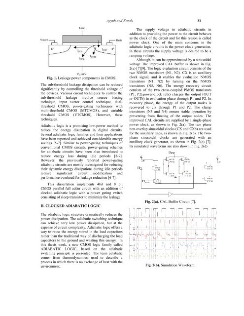
Ayyub and Kandu 33Fig. 1. Leakage power components in <strong>CMOS</strong>.The sub-threshold leakage dissipation can be reducedsignificantly by controlling the threshold voltage ofthe devices. Various circuit techniques to control thesub-threshold leakage involve source biasingtechnique, input vector control technique, dualthreshold<strong>CMOS</strong>, power-gating techniques withmulti-threshold <strong>CMOS</strong> (MT<strong>CMOS</strong>), and variablethreshold <strong>CMOS</strong> (VT<strong>CMOS</strong>), However, thesetechniques.Adiabatic logic is a promising low-power method toreduce the energy dissipation in digital circuits.Several adiabatic logic families and their applicationshave been reported and achieved considerable energysavings [5-7]. Similar to power-gating techniques ofconventional <strong>CMOS</strong> circuits, power-gating schemes<strong>for</strong> adiabatic circuits have been also introduced toreduce energy loss during idle periods [8-9].However, the previously reported power-gatingadiabatic circuits are mostly investigated <strong>for</strong> reducingtheir dynamic energy dissipations during idle periodsrequire significant circuit modification andper<strong>for</strong>mance overhead <strong>for</strong> leakage reduction [6-7].This dissertation implements 4bit and 8 bit<strong>CMOS</strong> parallel full adder circuit with an addition ofclocked adiabatic logic with a power gating switchconsisting of sleep transistor to minimize the leakageII. CLOCKED ADIABATIC LOGICThe adiabatic logic structure dramatically reduces thepower dissipation. The adiabatic switching techniquecan achieve very low power dissipation, but at theexpense of circuit complexity. Adiabatic logic offers away to reuse the energy stored in the load capacitorsrather than the traditional way of discharging the loadcapacitors to the ground and wasting this energy. Inthis thesis work, a new <strong>CMOS</strong> logic family calledADIABATIC LOGIC, based on the adiabaticswitching principle is presented. The term adiabaticcomes from thermodynamics, used to describe aprocess in which there is no exchange of heat with theenvironment.The supply voltage in adiabatic circuits inaddition to providing the power to the circuit behavesas the clock of the circuit and <strong>for</strong> this reason is calledpower clock. One of the main concerns in theadiabatic logic circuits is the power clock generation.In these circuits the supply voltage is desired to be aramping voltage.Although. it can be approximated by a sinusoidalvoltage The improved CAL buffer is shown in Fig.2(a) [7][9]. The logic evaluation circuit consists of thetwo NMOS transistors (N1, N2). CX is an auxiliaryclock signal, and it enables the evaluation NMOStransistors (N1, N2) by turning on the NMOStransistors (N5, N6). The energy recovery circuitconsists of the two cross-coupled PMOS transistors(P1, P2).power-clock ( clk) charges the output ( OUTor OUTb) in evaluation phase through P1 and P2. Inrecovery phase, the energy of the output nodes isrecovered to clk through P1 and P2. The clamptransistors (N3 and N4) ensure stable operat ion bypreventing from floating of the output nodes. Theimproved CAL circuits are supplied by a single-phasepower clock, as shown in Fig. 2(a). The two phasenon-overlap sinusoidal clocks (CX and CXb) are used<strong>for</strong> the auxiliary lines, as shown in Fig. 2(b). The twophasesinusoidal clocks are generated with anauxiliary clock generator, as shown in Fig. 2(c) [7].Its simulated wave<strong>for</strong>ms are also shown in Fig. 2(d)Fig. 2(a). CAL Buffer <strong>Circuit</strong> [7].Fig. 2(b). Simulation Wave<strong>for</strong>m.