A Power Gating Switch for Low Power 8 Bit CMOS Full Adder Circuit
A Power Gating Switch for Low Power 8 Bit CMOS Full Adder Circuit
A Power Gating Switch for Low Power 8 Bit CMOS Full Adder Circuit

You also want an ePaper? Increase the reach of your titles
YUMPU automatically turns print PDFs into web optimized ePapers that Google loves.
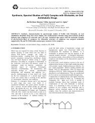
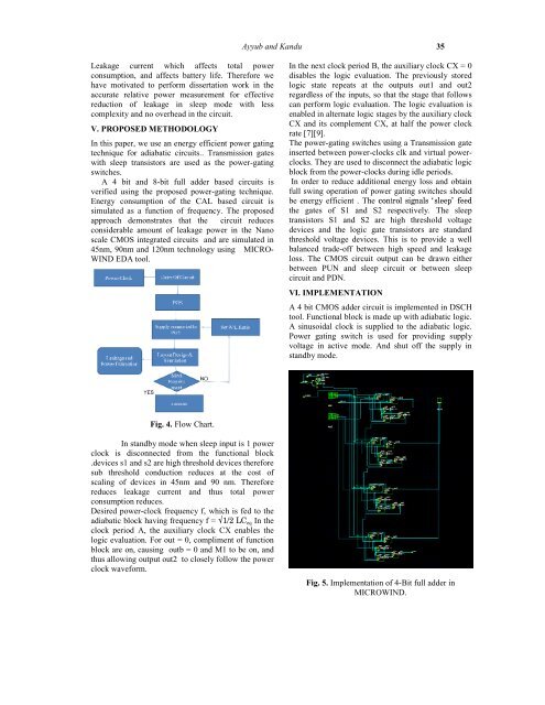
Ayyub and Kandu 35Leakage current which affects total powerconsumption, and affects battery life. There<strong>for</strong>e wehave motivated to per<strong>for</strong>m dissertation work in theaccurate relative power measurement <strong>for</strong> effectivereduction of leakage in sleep mode with lesscomplexity and no overhead in the circuit.V. PROPOSED METHODOLOGYIn this paper, we use an energy efficient power gatingtechnique <strong>for</strong> adiabatic circuits.. Transmission gateswith sleep transistors are used as the power-gatingswitches.A 4 bit and 8-bit full adder based circuits isverified using the proposed power-gating technique.Energy consumption of the CAL based circuit issimulated as a function of frequency. The proposedapproach demonstrates that the circuit reducesconsiderable amount of leakage power in the Nanoscale <strong>CMOS</strong> integrated circuits and are simulated in45nm, 90nm and 120nm technology using MICRO-WIND EDA tool.In the next clock period B, the auxiliary clock CX = 0disables the logic evaluation. The previously storedlogic state repeats at the outputs out1 and out2regardless of the inputs, so that the stage that followscan per<strong>for</strong>m logic evaluation. The logic evaluation isenabled in alternate logic stages by the auxiliary clockCX and its complement CX, at half the power clockrate [7][9].The power-gating switches using a Transmission gateinserted between power-clocks clk and virtual powerclocks.They are used to disconnect the adiabatic logicblock from the power-clocks during idle periods.In order to reduce additional energy loss and obtainfull swing operation of power gating switches shouldbe energy efficient . The control signals ‘sleep’ feedthe gates of S1 and S2 respectively. The sleeptransistors S1 and S2 are high threshold voltagedevices and the logic gate transistors are standardthreshold voltage devices. This is to provide a wellbalanced trade-off between high speed and leakageloss. The <strong>CMOS</strong> circuit output can be drawn eitherbetween PUN and sleep circuit or between sleepcircuit and PDN.VI. IMPLEMENTATIONA 4 bit <strong>CMOS</strong> adder circuit is implemented in DSCHtool. Functional block is made up with adiabatic logic.A sinusoidal clock is supplied to the adiabatic logic.<strong>Power</strong> gating switch is used <strong>for</strong> providing supplyvoltage in active mode. And shut off the supply instandby mode.Fig. 4. Flow Chart.In standby mode when sleep input is 1 powerclock is disconnected from the functional block.devices s1 and s2 are high threshold devices there<strong>for</strong>esub threshold conduction reduces at the cost ofscaling of devices in 45nm and 90 nm. There<strong>for</strong>ereduces leakage current and thus total powerconsumption reduces.Desired power-clock frequency f, which is fed to theadiabatic block having frequency f = √1/2 LC eq In theclock period A, the auxiliary clock CX enables thelogic evaluation. For out = 0, compliment of functionblock are on, causing outb = 0 and M1 to be on, andthus allowing output out2 to closely follow the powerclock wave<strong>for</strong>m.Fig. 5. Implementation of 4-<strong>Bit</strong> full adder inMICROWIND.