Advances in Silica Planar Lightwave Circuits - Next Generation ...
Advances in Silica Planar Lightwave Circuits - Next Generation ...
Advances in Silica Planar Lightwave Circuits - Next Generation ...

Create successful ePaper yourself
Turn your PDF publications into a flip-book with our unique Google optimized e-Paper software.
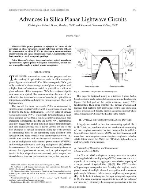
JOURNAL OF LIGHTWAVE TECHNOLOGY, VOL. 24, NO. 12, DECEMBER 2006 4763<strong>Advances</strong> <strong>in</strong> <strong>Silica</strong> <strong>Planar</strong> <strong>Lightwave</strong> <strong>Circuits</strong>Christopher Richard Doerr, Member, IEEE, and Katsunari Okamoto, Fellow, IEEEInvited PaperAbstract—This paper presents a synopsis of some of theadvances <strong>in</strong> silica waveguide planar lightwave circuits (PLCs).It concentrates on silica PLCs for fiber-optic communications,ma<strong>in</strong>ly rout<strong>in</strong>g and signal process<strong>in</strong>g devices. A significant portionis devoted to arrayed waveguide grat<strong>in</strong>gs.Index Terms—Grat<strong>in</strong>gs, <strong>in</strong>tegrated optics, optical equalizers,optical fibers, optical planar waveguide components, optical planarwaveguide couplers, optical planar waveguides.I. INTRODUCTIONTHIS PAPER summarizes some of the progress and understand<strong>in</strong>gof optical devices made <strong>in</strong> silica waveguideplanar lightwave circuits (PLCs). <strong>Silica</strong> waveguide PLCs typicallyconsist of a planar arrangement of glass waveguides witha higher <strong>in</strong>dex of refraction buried <strong>in</strong> glass all on a silicon orglass substrate. <strong>Silica</strong> waveguide PLCs have enjoyed significantsuccess <strong>in</strong> optical fiber communications because of theirreliability, low <strong>in</strong>sertion loss, ease of coupl<strong>in</strong>g to optical fibers,<strong>in</strong>tegration capability, and ability to produce optical filters withhigh accuracy.The market for silica waveguide PLCs is dom<strong>in</strong>ated bysimple optical couplers/splitters with a recent surge <strong>in</strong> sales dueto fiber-to-the-home deployments. However, sales of arrayedwaveguide grat<strong>in</strong>g (AWG) wavelength de/multiplexers, a muchmore complex device than a simple coupler/splitter, have been<strong>in</strong>creas<strong>in</strong>g significantly s<strong>in</strong>ce the late 1990s. AWG performancecan now exceed that of th<strong>in</strong>-film filter-based de/multiplexers,and their manufactur<strong>in</strong>g cost is lower. AWGs are one of thefirst examples of optical <strong>in</strong>tegration liv<strong>in</strong>g up to the promiseof elim<strong>in</strong>at<strong>in</strong>g most of the pa<strong>in</strong>stak<strong>in</strong>g hand assembly fromoptical devices. More recently, even more complex devices, i.e.,AWGs with switches and variable optical attenuators (VOAs)to act as multiplexers with channel power control (VMUXs)and reconfigurable optical add–drop multiplexers (ROADMs),have seen successful <strong>in</strong> the market. These are <strong>in</strong>tersignal controldevices. Intrasignal control devices, such as optical equalizers(which <strong>in</strong>clude dispersion compensators), pulse shapers, anddemodulators, have not had market success yet but may soon.Manuscript received May 16, 2006; revised August 14, 2006.C. R. Doerr is with Lucent Technologies, Bell Laboratories, Holmdel, NJ07733 USA (e-mail: crdoerr@lucent.com).K. Okamoto is with the Department of Electrical and Computer Eng<strong>in</strong>eer<strong>in</strong>g,University of California, Davis, CA 95616 USA (e-mail: katsu@okamotolab.com).Color versions of Figs. 6, 8, 15, 16, 19–23, 31, 35, 37–42, 45–49, and 51 areavailable onl<strong>in</strong>e at http://ieeexplore.ieee.org.Digital Object Identifier 10.1109/JLT.2006.885255Fig. 1.Schematic configuration of AWG multiplexer.This paper is designed ma<strong>in</strong>ly as a tutorial. It gives both abroad overview and a detailed discussion on some fundamentaltopics. The first part of this paper discusses ma<strong>in</strong>ly AWGfundamentals. Then, more complex PLC devices are discussed.Devices that perform both <strong>in</strong>tersignal control and <strong>in</strong>trasignalcontrol are discussed. F<strong>in</strong>ally, there is a conclusion about wheresilica waveguide PLCs may be headed <strong>in</strong> the future.II. OPTICAL FILTERING/MULTIPLEXING DEVICESA highly successful method for construct<strong>in</strong>g optical filters<strong>in</strong> PLCs is to use <strong>in</strong>terferometers. An <strong>in</strong>terferometer consist<strong>in</strong>gof two couplers connected by two waveguides is called aMach–Zehnder <strong>in</strong>terferometer (MZI). An <strong>in</strong>terferometer withmore than two waveguides connect<strong>in</strong>g two couplers is called anAWG. Other names for AWGs are PHASARs (phased arrays)and waveguide grat<strong>in</strong>g routers.A. Pr<strong>in</strong>ciple of Operation and FundamentalCharacteristics of AWGsAn N × N AWG multiplexer is very attractive <strong>in</strong> opticalwavelength-division multiplex<strong>in</strong>g (WDM) networks s<strong>in</strong>ce it iscapable of <strong>in</strong>creas<strong>in</strong>g the aggregate transmission capacity ofa s<strong>in</strong>gle strand of optical fiber [1]–[3]. The AWG consistsof <strong>in</strong>put/output waveguides, two focus<strong>in</strong>g slab regions, and aphased array of multiple channel waveguides with a constantpath length difference ∆L between neighbor<strong>in</strong>g waveguides(Fig. 1). In the first slab region, the <strong>in</strong>put waveguide separationis D 1 , the array waveguide separation is d 1 , and the radius ofcurvature is f 1 . Generally, the waveguide parameters <strong>in</strong> the first0733-8724/$20.00 © 2006 IEEE
4764 JOURNAL OF LIGHTWAVE TECHNOLOGY, VOL. 24, NO. 12, DECEMBER 2006where β s and β c denote the propagation constants <strong>in</strong> the slabregion and the array waveguide, respectively, m is an <strong>in</strong>teger,λ 0 is the center wavelength of the WDM system, and L c is them<strong>in</strong>imum array waveguide length. Subtract<strong>in</strong>g common termsfrom (1), we obta<strong>in</strong>β s (λ 0 ) d 1x 1f 1When the condition β c λ 0 ∆L =2mπ or− β s (λ 0 ) dxf + β c(λ 0 )∆L =2mπ. (2)λ 0 = n c∆Lm(3)is satisfied for λ 0 , the light <strong>in</strong>put position x 1 and the outputposition x should satisfy the conditiond 1 x 1f 1= dxf . (4)Fig. 2. Enlarged view of the second slab region (rotated 180 ◦ from Fig. 1).and second slab regions may be different. Therefore, <strong>in</strong> thesecond slab region, the output waveguide separation is D, thearray waveguide separation is d, and the radius of curvature is f.The <strong>in</strong>put light at position x 1 (x 1 is measured <strong>in</strong> a counterclockwisedirection from the center of <strong>in</strong>put waveguides) is radiatedto the first slab and then excites the arrayed waveguides.The excited electric field amplitude <strong>in</strong> each array waveguideis a i (i =1− N), where N is the total number of arraywaveguides. The amplitude profile a i is usually a Gaussiandistribution. After travel<strong>in</strong>g through the arrayed waveguides,the light beams constructively <strong>in</strong>terfere <strong>in</strong>to one focal po<strong>in</strong>t x(x is measured <strong>in</strong> a counterclockwise direction from the centerof output waveguides) <strong>in</strong> the second slab. The location of thisfocal po<strong>in</strong>t depends on the signal wavelength s<strong>in</strong>ce the relativephase delay <strong>in</strong> each waveguide is given by ∆L/λ.Fig.2showsan enlarged view of the second slab region. Let us consider thephase retardations for the two light beams pass<strong>in</strong>g through the(i − 1)th and ith array waveguides. The geometrical distancesof two beams <strong>in</strong> the second slab region are approximated asshown <strong>in</strong> Fig. 2. We have similar configurations <strong>in</strong> the firstslab region as those <strong>in</strong> Fig. 2. The difference of the totalphase retardations for the two light beams pass<strong>in</strong>g through the(i − 1)th and ith array waveguides must be an <strong>in</strong>teger multipleof 2π <strong>in</strong> order that the two beams constructively <strong>in</strong>terfere atthe focal po<strong>in</strong>t x. Therefore, we have the <strong>in</strong>terference conditionexpressed by(β s (λ 0 ) f 1 − d )(1x 1+β c (λ 0 )[L c +(i−1)∆L]+β s (λ 0 ) f + dx )2f 1 2f(= β s (λ 0 ) f 1 + d )1x 1+β c (λ 0 )[L c +i∆L]2f 1(+ β s (λ 0 ) f − dx2f)−2mπ (1)In (3), n c is the effective <strong>in</strong>dex of the array waveguide (2πn c =β c /k k: wavenumber <strong>in</strong> vacuum), and m is called the diffractionorder. The above equation means that when light is coupled <strong>in</strong>tothe <strong>in</strong>put position x 1 , the output position x is determ<strong>in</strong>ed by (4).Usually, the waveguide parameters <strong>in</strong> the first and second slabregions are the same (d 1 = d and f 1 = f). Therefore, the <strong>in</strong>putand output distances are equal as x 1 = x. The spatial dispersionof the focal position x with respect to the wavelength λ for thefixed light <strong>in</strong>put position x 1 is given by differentiat<strong>in</strong>g (2) withrespect to λ as∆x∆λ = −N cf∆L(5)n s dλ 0where n s is the effective <strong>in</strong>dex <strong>in</strong> the slab region, and N c is the“group” <strong>in</strong>dex of the effective <strong>in</strong>dex n c of the array waveguide(N c = n c − λdn c /dλ). The spatial dispersion of the <strong>in</strong>put sideposition x 1 with respect to the wavelength λ for fixed lightoutput position x is given by∆x 1∆λ = N cf 1 ∆Ln s d 1 λ 0. (6)The <strong>in</strong>put and output waveguide separations are |∆x 1 | = D 1and |∆x| = D, respectively, when ∆λ is the channel spac<strong>in</strong>gof the WDM signal. Putt<strong>in</strong>g these relations <strong>in</strong>to (5) and (6), thewavelength spac<strong>in</strong>g on the output side for a fixed light <strong>in</strong>putposition x 1 is given by∆λ out = n sdDλ 0N c f∆Land the wavelength spac<strong>in</strong>g on the <strong>in</strong>put side for a fixed lightoutput position x is given by(7)∆λ <strong>in</strong> = n sd 1 D 1 λ 0N c f 1 ∆L . (8)Often, the waveguide parameters <strong>in</strong> the first and second slabregions are the same, i.e., D 1 = D, d 1 = d, and f 1 = f. Then,
DOERR AND OKAMOTO: ADVANCES IN SILICA PLANAR LIGHTWAVE CIRCUITS 4765For further read<strong>in</strong>g on AWG fundamentals, see [4]–[6]and [10].Fig. 3. BPM simulation of the light-focus<strong>in</strong>g property <strong>in</strong> the second slabregion (rotated −90 ◦ from Fig. 1) for the (a) central wavelength λ 0 and(b) shorter wavelength component λ
4766 JOURNAL OF LIGHTWAVE TECHNOLOGY, VOL. 24, NO. 12, DECEMBER 2006Fig. 4.Demultiplex<strong>in</strong>g properties of 32-channel 50-GHz-spac<strong>in</strong>g AWG over four diffraction orders.Fig. 5.Demultiplex<strong>in</strong>g properties of 400-channel 25-GHz-spac<strong>in</strong>g AWG.Fig. 6.Demultiplex<strong>in</strong>g properties of 32-channel 10-GHz-spac<strong>in</strong>g AWG.is the ideal effective <strong>in</strong>dex distribution, δn is an amplitudeof fluctuation, and Λ is a half period of <strong>in</strong>dex fluctuation.It is known empirically that crosstalk degrades by about5 dB when the channel spac<strong>in</strong>g is cut <strong>in</strong> half. It is alsoknown that crosstalk degrades by about 10 dB when δn becomesabout 3.2 (= √ 10) times larger. For the phase fluctuations,the sidelobe level strongly depends on the channelspac<strong>in</strong>g.
DOERR AND OKAMOTO: ADVANCES IN SILICA PLANAR LIGHTWAVE CIRCUITS 4767Fig. 7. Theoretical demultiplex<strong>in</strong>g properties of AWGs hav<strong>in</strong>g s<strong>in</strong>usoidalphase fluctuation of δn =1× 10 −6 with Λ=N/10 for three k<strong>in</strong>ds of AWGswith 100-, 50-, and 25-GHz channel spac<strong>in</strong>g.2) Dispersion of AWG: Phase errors cause not onlycrosstalk but also chromatic dispersion <strong>in</strong> the AWG itself [11].Fig. 8 shows the theoretical dispersion properties of 64-channel100-GHz-spac<strong>in</strong>g to 64-channel 25-GHz-spac<strong>in</strong>g AWGs hav<strong>in</strong>gspatially s<strong>in</strong>usoidal phase fluctuations given by (12). It isshown that a spatially low-frequency phase fluctuation (small s)causes dispersion <strong>in</strong>side the passband of the AWG. Here,dispersion values are fixed to be −15 ps/nm <strong>in</strong> Fig. 8(a)–(c)and +15 ps/nm <strong>in</strong> Fig. 8(d)–(f). Then, the <strong>in</strong>dex fluctuation δnthat generates the specified dispersion is calculated. It is knownempirically from several calculations, <strong>in</strong>clud<strong>in</strong>g Fig. 8, that thedependence of dispersion σ on <strong>in</strong>dex fluctuation δn and channelspac<strong>in</strong>g ∆ν is approximately obta<strong>in</strong>ed as σ ∝ δn/∆ν 3 . S<strong>in</strong>ceσ is <strong>in</strong>versely proportional to ∆ν 3 , the dispersion of an AWGwith a narrow channel spac<strong>in</strong>g is much more susceptible tophase errors.D. Flat Spectral Response AWGsS<strong>in</strong>ce the rate of displacement of the focal position x withrespect to the wavelength λ is almost constant (5), the transmissionloss of a Gaussian AWG monotonically <strong>in</strong>creasesaround the center wavelength of each channel. This places tightrestrictions on the wavelength tolerance of lasers and requiresaccurate temperature control for the AWGs. Moreover, s<strong>in</strong>ceoptical signals may be transmitted through several filters <strong>in</strong>WDM r<strong>in</strong>g/bus networks, the cumulative passband width ofeach channel becomes much narrower than that of a s<strong>in</strong>glestageAWG filter. One solution is to make the Gaussian AWGpassband very wide compared to the channel spac<strong>in</strong>g, as discussed<strong>in</strong> Section II-F1. This may be acceptable when theAWG is used as a multiplexer. However, it is not acceptablewhen the AWG is used as a demultiplexer because of the highcrosstalk due to overlapp<strong>in</strong>g adjacent passbands. Therefore,flattened and broadened spectral responses with steep spectralskirts (i.e., a rectangular passband) are often required for AWGdemultiplexers.Several approaches have been proposed to flatten the passbandsof AWGs [12]–[17]. One is to create a flat electricfield distribution at the <strong>in</strong>put waveguide. S<strong>in</strong>ce the AWG isan imag<strong>in</strong>g device, the flat electric field is reproduced at theoutput plane. The overlap <strong>in</strong>tegral of a flat field with a Gaussianlocal normal mode gives a flat spectral response. Parabolicwaveguide horns [13] or 1 × 2 multimode <strong>in</strong>terference couplers[14] are used to create a flat electric field distribution at the <strong>in</strong>putwaveguide. The second method is to eng<strong>in</strong>eer the waveguidearray design to create a flattened electric field at the outputplane. In this case, the <strong>in</strong>put field is a normal Gaussian distribution.There are ma<strong>in</strong>ly two techniques to achieve this secondmethod. One is to make a s<strong>in</strong>c-like electric field envelope <strong>in</strong> thearray waveguides [12]. S<strong>in</strong>ce the focused electric field profile isa Fourier-transformed image of the electric field <strong>in</strong> the arraywaveguides, we can generate a flattened field distribution atthe output plane. The other is to make two focal spots at theoutput plane [15]. Here, the light-focus<strong>in</strong>g direction of thearray waveguide is alternately changed to two separate focalpositions. In this case, the flattened field profile consists of twoGaussian beams.There are some other flatten<strong>in</strong>g techniques employ<strong>in</strong>g somewhatsophisticated operational pr<strong>in</strong>ciples [16], [17]. In thesetechniques, the <strong>in</strong>put position of the beam moves synchronouslywith the wavelength change of the signal, and they are discussed<strong>in</strong> Section II-E. Then, the output beam lies <strong>in</strong> a fixed position<strong>in</strong>dependent of wavelength with<strong>in</strong> one channel span.1) Parabola-Type AWG: The <strong>in</strong>set <strong>in</strong> Fig. 9 shows an enlargedview of a parabola-shaped <strong>in</strong>put waveguide. The widthof the parabolic horn along the propagation direction z is givenby [18]√W (z) = 2αλ g z +(2a) 2 (13)where α is a constant less than unity, λ g is the wavelength <strong>in</strong>the guide (λ g = λ/n c ), and 2a is the core width of the channelwaveguide. At the proper horn length z = l less than the collimatorlength, a slightly double-peaked <strong>in</strong>tensity distributioncan be obta<strong>in</strong>ed, as shown <strong>in</strong> Fig. 9. A broadened and sharpfall<strong>in</strong>goptical <strong>in</strong>tensity profile is obta<strong>in</strong>able by the parabolicwaveguide horn, which is quite advantageous for achiev<strong>in</strong>ga wide passband without deteriorat<strong>in</strong>g the nearest-neighborcrosstalk characteristics. The broadened and double-peakedfield is imaged onto the entrance of an output waveguide hav<strong>in</strong>ga normal core width. The overlap <strong>in</strong>tegral of the focused fieldwith the local normal mode of the output waveguide gives a flattenedspectral response for the AWG. Fig. 10 shows the demultiplex<strong>in</strong>gproperties of a 32-channel 100-GHz-spac<strong>in</strong>g AWGhav<strong>in</strong>g parabolic horns with W =26.1 µm and l = 270 µm.In a parabola-type flat AWG, the double-peaked electric fielddistribution is created by the <strong>in</strong>terference of the fundamentalmode and the second-order mode. Generally, the phaseretardations of the fundamental mode and second-ordermode are different. Therefore, the total phase at the end of theparabolic waveguide horn is not a uniform phase distribution. Anonuniform phase distribution <strong>in</strong> the parabola <strong>in</strong>put waveguide
4768 JOURNAL OF LIGHTWAVE TECHNOLOGY, VOL. 24, NO. 12, DECEMBER 2006Fig. 8.Theoretical dispersion characteristics of three k<strong>in</strong>ds of AWGs with 100-, 50-, and 25-GHz channel spac<strong>in</strong>g for various k<strong>in</strong>ds of <strong>in</strong>dex fluctuation δn.Fig. 9. Intensity profile calculated by the BPM <strong>in</strong> the parabolic <strong>in</strong>putwaveguide. Inset shows the schematic configuration of parabolic waveguide.causes nonuniformity of phase <strong>in</strong> the array waveguides. It isknown that such a nonuniform phase is similar to effective<strong>in</strong>dex fluctuations <strong>in</strong> the array waveguides and thus can causechromatic dispersion as described <strong>in</strong> the previous section.Fig. 11 shows the theoretical and experimental dispersion characteristicsof a 32-channel 100-GHz parabola-type flat AWG.Phase retardations between the fundamental and the secondordermodes at the end of the parabolic waveguide horn can beadjusted by add<strong>in</strong>g a straight multimode waveguide, as shown<strong>in</strong> Fig. 12 [19]. At the proper multimode waveguide length,phase retardations of the fundamental and second-order modesare almost equalized. The total phase distribution becomesuniform while the double-peaked electric field distributionis ma<strong>in</strong>ta<strong>in</strong>ed. The theoretical and experimental dispersioncharacteristics of the 32-channel 100-GHz parabola-type flatAWG with W =26.1 µm, l = 270 µm, and L multi =85µmFig. 10. Demultiplex<strong>in</strong>g properties of 32-channel 100-GHz-spac<strong>in</strong>g AWGhav<strong>in</strong>g parabolic horns with W =26.1 µm andl = 270 µm.are shown <strong>in</strong> Fig. 13. Chromatic dispersion has been reducedto a negligible value.E. AWGs With Periodic Stationary Imag<strong>in</strong>g1) Achiev<strong>in</strong>g Multiple Zero-Loss Maxima: As discussed <strong>in</strong>the previous section, when optical filters, such as a wavelengthdemultiplexer, are used <strong>in</strong> WDM fiber-optic communicationsystems, it is often desirable that the passband magnitude havea rectangular shape and the passband phase change l<strong>in</strong>earlywith optical frequency. A rectangular shape means that thepassband magnitude is flat on top and falls off steeply on bothsides. Such a filter distorts signals pass<strong>in</strong>g through it very little(provided the passband is wide enough) and can be cascaded(many such filters encountered <strong>in</strong> series) with low net signal
DOERR AND OKAMOTO: ADVANCES IN SILICA PLANAR LIGHTWAVE CIRCUITS 4769Fig. 11. Theoretical and experimental dispersion characteristics of a32-channel 100-GHz parabola-type flat AWG.Fig. 12.Parabolic waveguide hav<strong>in</strong>g a straight multimode waveguide.distortion. A l<strong>in</strong>ear phase means that the passband has zerochromatic dispersion.How rectangular a passband is can be quantified by the numberof maxima <strong>in</strong> the passband. For <strong>in</strong>stance, a standard AWGhas a Gaussian-shaped passband, which has one maximum <strong>in</strong>the passband. Such a passband is far from be<strong>in</strong>g rectangular.However, if we have two maxima <strong>in</strong> the passband, then alreadythe passband starts to look rectangular. The maxima <strong>in</strong> the passbandcan be at different frequencies or at the same frequency.When many of the same optical filter are placed <strong>in</strong> series, thenet cascaded passband is simply a stretch<strong>in</strong>g of the scale of thepassband if it is plotted <strong>in</strong> decibels (<strong>in</strong> actuality, small variationfrom filter to filter complicates this). For example, the 0.3-dBdown po<strong>in</strong>t on the passband becomes the 3-dB down po<strong>in</strong>tafter ten cascades. The passband shape is stretched downwardaround the maxima. Thus, the more maxima (provided themaxima are at the same magnitude), the more the passband is“held open.”As shown <strong>in</strong> Section II-D, one way to add more maxima to anAWG passband is through image mismatch<strong>in</strong>g, i.e., the imageFig. 13. Theoretical and experimental dispersion characteristics of 32-channel100-GHz parabola-type flat AWG with W =26.1 µm, l = 270 µm, andL multi =85µm.from the <strong>in</strong>put waveguide does not match the image that anoutput waveguide would make. Such a method is compact androbust. However, image mismatch<strong>in</strong>g adds optical loss. Thissection addresses add<strong>in</strong>g maxima without add<strong>in</strong>g loss.Any optical filter can be represented <strong>in</strong> the time doma<strong>in</strong> byits impulse response. For the discussion here, we will limitourselves to optical filters that are periodic, with a free spectralrange (FSR) equal to ∆f. Thus, the time-doma<strong>in</strong> impulsesare spaced by 1/∆f. If a filter has one zero-loss maximumper FSR, then the sum of the magnitudes of the impulses (<strong>in</strong>optical amplitude, not power) is equal to a zero-loss maximum<strong>in</strong> the spectrum. If a filter has more than one zero-lossmaximum per FSR, then this sum must be greater than unity.Otherwise, all the impulses must be <strong>in</strong> phase to achieve a zerolossmaximum <strong>in</strong> the spectrum, and this can happen only onceper FSR.The impulse response of an optical filter is measured bysend<strong>in</strong>g an impulse <strong>in</strong>to the filter and record<strong>in</strong>g the impulsesthat exit the filter. Each possible path through the filter generatesan impulse. Not every path generates an <strong>in</strong>dependentimpulse s<strong>in</strong>ce multiple paths may have the same length. Fora periodic filter, all path lengths are an <strong>in</strong>teger multiple of a unitlength.If the filter consists of a 1 × N coupler, N arms, and anN × 1 coupler, i.e., an MZI (if N =2) or an AWG (if N>2),then the sum of the impulse amplitude magnitudes cannot begreater than one; otherwise, power conservation is violated.This is because each impulse is generated by one arm, so itis possible that at some frequency all impulses are <strong>in</strong> phase.Thus, it is impossible for an AWG to have more than one zerolossmaximum per passband per FSR, regardless of what armlength distribution, <strong>in</strong>put mode shape, or output mode shapeis chosen. Furthermore, concatenat<strong>in</strong>g such filters, which arefilters <strong>in</strong>terconnected by a s<strong>in</strong>gle mode, cannot create a net filterwith an impulse response magnitude sum that is greater thanunity because the convolution of two impulse tra<strong>in</strong>s each witha magnitude sum that is not greater than unity cannot have amagnitude sum that is greater than unity.
4770 JOURNAL OF LIGHTWAVE TECHNOLOGY, VOL. 24, NO. 12, DECEMBER 2006Fig. 14. Fourier-filter-based <strong>in</strong>terleaver and concept for achiev<strong>in</strong>g zero dispersion with 2 × 2 filters. As one can see, the port-pair comb<strong>in</strong>ation <strong>in</strong> the left stageis complementary to the port-pair comb<strong>in</strong>ation <strong>in</strong> the right stage.Thus, we have proven the follow<strong>in</strong>g theorem.Theorem 1: It is impossible to generate more than one zerolossmaximum per FSR if the filter conta<strong>in</strong>s only 1 × N (or,equivalently, N × 1) couplers.Then, how can one generate an impulse response with amagnitude sum greater than unity? The answer is to use atleast one M × N coupler, where M, N>1. Such a couplercan generate “extra” impulses such that one waveguide can beresponsible for generat<strong>in</strong>g more than one impulse.A good example of this is the Fourier filter <strong>in</strong>terleaver, shown<strong>in</strong> Fig. 14. This filter can theoretically have zero loss at twowavelengths per FSR, because it conta<strong>in</strong>s one 2 × 2 coupler.Such a filter has a chromatic dispersion. However, this can beovercome by cascad<strong>in</strong>g two identical filters <strong>in</strong> series, whereone connects one port of the first filter to the complementaryport of the second filter [20]. This works because <strong>in</strong> a 2 × 2filter, the amplitude transmissivity from one <strong>in</strong>put port to oneoutput port is equal to the complex conjugate of the amplitudetransmissivity between the other <strong>in</strong>put port to the otheroutput port.2) AWG With Two-Arm-Interferometer Input: Us<strong>in</strong>g the theoremwe just proved, we realize that a conventional AWG canhave only one zero-loss maximum per FSR. In this section,we would like to create an AWG with two zero-loss maximaper FSR. To do this, we will have to connect the device<strong>in</strong>put to more than one <strong>in</strong>put to the first AWG star coupler(or equivalently connect the device output to more than oneoutput from the second AWG star coupler).To figure out what to connect between the device <strong>in</strong>putand the two star coupler <strong>in</strong>puts, note that the problem with aconventional AWG is that the image <strong>in</strong> the second star coupleris always mov<strong>in</strong>g as the wavelength <strong>in</strong>creases. To create twozero-loss maxima per FSR, we need to have the image focus onthe output waveguide <strong>in</strong> the second star coupler twice per FSR.To do this, we need to move the image <strong>in</strong> the first star coupleras the wavelength changes. We can accomplish this by hav<strong>in</strong>g alength-imbalanced MZI connected to the two <strong>in</strong>puts of the firststar coupler, where light moves from one <strong>in</strong>put to the secondas the wavelength changes such that both images focus on thesame output waveguide [17], [21]. If we then match the FSR ofthe MZI to the channel spac<strong>in</strong>g of the AWG, then one MZI cancreate dual zero-loss maxima for all channels.Fig. 15. Change <strong>in</strong> optical field at end of a length-imbalanced MZI with adirectional 2 × 2 coupler as the optical frequency is changed.Fig. 15 shows a plot of the optical power from the MZI atthe MZI–star coupler junction as the wavelength changes. Thelight switches from one output to the other. In between thesestates, the light is partly <strong>in</strong> one output or the other. One canview the “center of mass” of the optical distribution as mov<strong>in</strong>gcont<strong>in</strong>uously between the two states. S<strong>in</strong>ce this is imaged bythe AWG onto the output waveguide, one can view the MZI asmak<strong>in</strong>g the center of mass of the image stationary on the outputwaveguide. This is what creates the desired low-loss flat-toppassband.Two possible ways of lay<strong>in</strong>g out the MZI-AWG are shown<strong>in</strong> Fig. 16. Fig. 16(a) shows the MZI and AWG hav<strong>in</strong>g thesame sign of “curvature.” This is necessary for the synchronizationof the MZI and AWG at their <strong>in</strong>terconnection po<strong>in</strong>t.Fig. 16(b) shows a switch<strong>in</strong>g of the sign of curvature. This ispossible by hav<strong>in</strong>g a sort of waveguide cross<strong>in</strong>g <strong>in</strong> the MZI,that is effected by us<strong>in</strong>g a 100/0 coupler. It is found that arelative phase shift of 180 ◦ between the waveguides connect<strong>in</strong>gthe 100/0 coupler to the 50/50 coupler m<strong>in</strong>imizes the performancesensitivity to wavelength, fabrication, and polarizationchanges.Fig. 17 shows an actual waveguide layout and the result<strong>in</strong>gmeasured transmissivity. Theoretically, the chromatic
DOERR AND OKAMOTO: ADVANCES IN SILICA PLANAR LIGHTWAVE CIRCUITS 4771wouldlikeittobe120 ◦ because this is the phase differenceencountered <strong>in</strong> an ideal star coupler. The phase between port m 1on one side and m 2 on the other side of an ideal M × M starcoupler isφ = 2πM(m 1 − M +1 )(m 2 − M +1 ). (14)22Fig. 16. Possible layouts for a rectangular passband demultiplexer consist<strong>in</strong>gof an MZI directly connected to an AWG.dispersion <strong>in</strong> the passband is zero. However, if the 50/50coupler has a splitt<strong>in</strong>g ratio error, then the device will exhibitdispersion. This can be understood by follow<strong>in</strong>g a signal pass<strong>in</strong>gfrom right to left through the device. Suppose the 50/50coupler is too weak. Then, when the signal from the AWG isimaged onto the upper waveguide of the 50/50 coupler, whichis the short-wavelength side of the passband, then <strong>in</strong>stead ofthe signal be<strong>in</strong>g divided evenly between the two MZI arms,more light will be coupled to the longer MZI arm. The effectivepath length through an <strong>in</strong>terferometer is equal to the averageof the path lengths weighted by the optical power <strong>in</strong> each arm.Thus, the total path length through the device will be longeron the shorter-wavelength side of the passband. It will be viceversafor the longer wavelength portion. Thus, the passband willexhibit negative dispersion.3) AWG With Three-Arm Interferometer Input: We justshowed how to create a passband with two zero-loss maximaby connect<strong>in</strong>g a two-arm <strong>in</strong>terferometer to an AWG. Onecan extend this pr<strong>in</strong>ciple by us<strong>in</strong>g a larger number of arms<strong>in</strong> the <strong>in</strong>put <strong>in</strong>terferometer. However, many difficult technicalchallenges arise once the number of arms is greater than two.Here, we address them for an arm number of three [22], [23].The ma<strong>in</strong> challenge with go<strong>in</strong>g from two arms to three armsis the directional coupler that connects to the AWG. As we willshow, a three-arm directional coupler is not trivial, and it ishas an undesirable phase relationship between the outputs. Onemight th<strong>in</strong>k why not turn the <strong>in</strong>put <strong>in</strong>terferometer <strong>in</strong>to a smallAWG and use a star coupler? However, a star coupler with a lowport count (∼< 8) has a very low efficiency, undo<strong>in</strong>g our <strong>in</strong>tentof mak<strong>in</strong>g a low-loss flat-top passband. A star coupler with alow port count has a low efficiency because the waveguides convergetoo quickly to convert the plane waves of the free-spaceregion to only first-order Bloch modes of the waveguide array.The problem with the three-waveguide directional coupleris that the difference of the phase between adjacent outputwaveguides from the coupler when illum<strong>in</strong>at<strong>in</strong>g one <strong>in</strong>putwaveguide of the coupler is always an <strong>in</strong>teger multiple of 90 ◦ ,whereas we would like it to be an <strong>in</strong>teger multiple of 120 ◦ .WeFor M =3, one can see that this gives either 0 ◦ or 120 ◦ phasedifference. The 90 ◦ phase difference encountered <strong>in</strong> the directionalcoupler means that the three passbands per FSR fromthe <strong>in</strong>put <strong>in</strong>terferometer are unequally spaced <strong>in</strong> frequency, andthe result<strong>in</strong>g <strong>in</strong>terferometer-plus-AWG device exhibits mostlya two zero-loss maxima passband. However, us<strong>in</strong>g a multisectionthree-waveguide directional coupler, one can achieve thedesired phase difference and achieve a three zero-loss maximapassband. The design and results are shown <strong>in</strong> Fig. 18.If we wish to use more than three arms and not use a starcoupler for the second coupler of the <strong>in</strong>put <strong>in</strong>terferometer, thenwe have a difficult problem with the design of the <strong>in</strong>put <strong>in</strong>terferometer.As shown <strong>in</strong> [24], if one makes a demultiplexer us<strong>in</strong>g amultimode <strong>in</strong>terference coupler (and likewise with a directionalcoupler), the arm lengths no longer follow a l<strong>in</strong>ear progression<strong>in</strong> path length when the arm number is greater than three.F. AWGs With High Spectral Sampl<strong>in</strong>gSuppose we have a conventional AWG with one <strong>in</strong>put andN outputs, and we launch a signal <strong>in</strong>to the <strong>in</strong>put. The N outputstake discrete “samples” of the spectrum of the <strong>in</strong>put signal,spaced <strong>in</strong> spectrum by a certa<strong>in</strong> amount and “filtered” by acerta<strong>in</strong> “bandwidth” [25]. This is analogous to sampl<strong>in</strong>g <strong>in</strong> thetime doma<strong>in</strong>, <strong>in</strong> which a waveform is sampled by discrete-timesample po<strong>in</strong>ts spaced <strong>in</strong> time by a certa<strong>in</strong> amount and filteredby a certa<strong>in</strong> “bandwidth.”1) Sampl<strong>in</strong>g Theorem: For the time-doma<strong>in</strong> case, if thespectrum is zero for frequency |f| >f B /2, and the signal issampled <strong>in</strong> time by spac<strong>in</strong>g T , then we can def<strong>in</strong>e a sampl<strong>in</strong>gcoefficients = 1 . (15)Tf BThe sampl<strong>in</strong>g theorem states that if s ≥ 1, then the signal isuniquely determ<strong>in</strong>ed by its samples.We can derive a similar relation for the AWG <strong>in</strong> the spectraldoma<strong>in</strong>. The field along one edge of a star coupler is approximatelythe spatial spectrum (i.e., Fourier transform) of the fieldalong the other edge. The output waveguides of the AWG arethus sampl<strong>in</strong>g the spatial spectrum of the field from the grat<strong>in</strong>garms. If we make this field zero outside of a spatial width w,and if the output waveguides are spaced closely enough, thenthe samples <strong>in</strong> the output waveguides can uniquely determ<strong>in</strong>ethe field along the grat<strong>in</strong>g arm edge of the output star coupler<strong>in</strong> the AWG. This field is determ<strong>in</strong>ed by the <strong>in</strong>put signalspectrum. Thus, we can uniquely determ<strong>in</strong>e the <strong>in</strong>put spectrumby these discrete samples. To make the field zero outside ofwidth w, we can simply use a limited number of grat<strong>in</strong>g arms<strong>in</strong> the AWG. w = Ma, where M is the number of grat<strong>in</strong>g
4772 JOURNAL OF LIGHTWAVE TECHNOLOGY, VOL. 24, NO. 12, DECEMBER 2006Fig. 17.Waveguide layout and measured results from a demultiplexer consist<strong>in</strong>g of an MZI directly connected to an AWG.Fig. 18.Sixteen-channel demultiplexer consist<strong>in</strong>g of a three-arm <strong>in</strong>terferometer directly connected to an AWG.arms, and a is the grat<strong>in</strong>g arm pitch at the connection to theoutput star coupler. Note that the star coupler can still havedummy waveguides outside of width w, to which the field cancouple, because the dummy waveguides are necessary for thestar coupler to perform an accurate Fourier transform.If the output waveguides have pitch b at their connection tothe output star coupler, then the sampl<strong>in</strong>g coefficient iss = Rλ(16)MabR is the star coupler radius (i.e., length), and λ is the wavelength<strong>in</strong> the slab (i.e., not the free-space wavelength). Thus, if s ≥ 1,the <strong>in</strong>formation <strong>in</strong> the output waveguides is sufficient touniquely determ<strong>in</strong>e the AWG <strong>in</strong>put signal. Note that becausethere are a f<strong>in</strong>ite number of output waveguides, the signalspectrum must be bandlimited for this to be true. It is analogousto the time-doma<strong>in</strong> case, <strong>in</strong> which the signal must be limited <strong>in</strong>its time extent because only a f<strong>in</strong>ite number of time sampl<strong>in</strong>gpo<strong>in</strong>ts can be recorded.Interest<strong>in</strong>gly, when s =1, the output star coupler is anM × M star coupler, although it is possible that less thanM output waveguides are actually used.One use for an AWG with high sampl<strong>in</strong>g is as a multiplexerwith passbands as wide as possible and no concern for crosstalk
DOERR AND OKAMOTO: ADVANCES IN SILICA PLANAR LIGHTWAVE CIRCUITS 4773Fig. 19. (Top) Mismatch <strong>in</strong> refractive <strong>in</strong>dex distribution at the slab-to-array transition <strong>in</strong> a star coupler, which is a significant source of <strong>in</strong>sertion loss <strong>in</strong> AWGs.(Bottom) Various demonstrated schemes for reduc<strong>in</strong>g this loss.level. Other uses <strong>in</strong>clude mak<strong>in</strong>g a dynamic ga<strong>in</strong> equalizationfilter (DGEF) and a band de/multiplexer, which is describedlater <strong>in</strong> this section.2) Aberrations: A conventional Gaussian passband AWGdemultiplexer has s ≈ 0.5. Ass is <strong>in</strong>creased toward 1 andbeyond, a significant problem <strong>in</strong> the AWG usually develops:the output waveguides become so close that there is significantmutual coupl<strong>in</strong>g between them. If left uncorrected, this results<strong>in</strong> aberrations that give high loss and large passband shoulders.To mitigate the mutual coupl<strong>in</strong>g, one could <strong>in</strong>crease b. However,this results <strong>in</strong> a longer R [see (16)] and a larger device size.A better solution is to move the aim<strong>in</strong>g po<strong>in</strong>t of the grat<strong>in</strong>gwaveguides <strong>in</strong>to the output waveguides and then slightly modifythe grat<strong>in</strong>g arm path lengths [26].To calculate how much to adjust the grat<strong>in</strong>g arm lengths, onemust calculate the transmissivity from each grat<strong>in</strong>g waveguidethrough the second star coupler to each output waveguide.When there is mutual coupl<strong>in</strong>g between the waveguides, auseful tool is BPM. Many types of BPM exist, such asFourier transform BPM (FT-BPM) and f<strong>in</strong>ite-difference BPM(FD-BPM). FT-BPM can handle wide angles but is slow andcannot handle large <strong>in</strong>dex steps. FD-BPM is much faster andcan handle large <strong>in</strong>dex steps but cannot handle wide angles.There is another type called s<strong>in</strong>c BPM [27], which is based onFT-BPM but stays <strong>in</strong> the angular spectrum doma<strong>in</strong>. It is fast andaccurate for periodic waveguide arrays, such as encountered <strong>in</strong>star couplers.To calculate the transmissivities mentioned earlier, wefirst calculate the waveguide mode of an uncoupled grat<strong>in</strong>gwaveguide. Then, we use BPM to propagate it until it reachesthe star coupler boundary. Call this field u 1 . Then, we calculatethe waveguide mode <strong>in</strong> an uncoupled output waveguide and useBPM to propagate it until it reaches the star coupler boundary.Call this field u 2 . The transmissivity although the second starcoupler <strong>in</strong> an AWG from a grat<strong>in</strong>g waveguide at angle θ 1 to anoutput waveguide at angle θ 2 is∫ ∞−∞t(θ 1 ,θ 2 )=uprop 1 (x)u 2 (x)exp[jkx(θ 2 − ∠AB)] dx√ ∫ ∞−∞ |u 1(x)| 2 dx ∫ ∞−∞ |u 2(x)| 2 dx(17)AB = R(e −jθ 1− 1+e jθ 2) (18)u prop1 (x) =F −1{ F {u 1 (x)exp[jkx(θ 1 − ∠AB)]}(× exp j √ )}k 2 − kx|AB|2 (19)F {u(x)} =∫ ∞−∞u(x)e jxk xdx. (20)In general, when design<strong>in</strong>g a star coupler with mutual coupl<strong>in</strong>gbetween waveguides, it is best to aim for mak<strong>in</strong>g u 1 andu 2 such that the power coupled to each of the two adjacentwaveguides is ∼4 dB less than the power <strong>in</strong> the launchedwaveguide. Increas<strong>in</strong>g the mutual coupl<strong>in</strong>g beyond this tendsto make the device too sensitive to fabrication details.Just as segmentation [28], vertical taper<strong>in</strong>g [29], or selectiveUV exposure [30] (see Fig. 19) improve the AWG grat<strong>in</strong>gefficiency, these techniques can also improve the coupl<strong>in</strong>gefficiency to highly sampled output waveguides. They work byreduc<strong>in</strong>g the abruptness of the transition from the waveguidearray to the slab region. Segmentation is the easiest to implements<strong>in</strong>ce it does not require any extra fabrication steps. Insegmentation, one simply adds sections (15 is a typical number)perpendicular to the waveguides. The section center-to-centerspac<strong>in</strong>g is constant, but their widths gradually decrease as theirdistance from the slab <strong>in</strong>creases.3) DGEF: In Section II-E1, we proved that we need N ×M couplers, where N, M>2 to create a passband with more
4774 JOURNAL OF LIGHTWAVE TECHNOLOGY, VOL. 24, NO. 12, DECEMBER 2006Fig. 20. DGEF consist<strong>in</strong>g of two AWGs connected by an AWL. Upper left is the concept, lower left is the actual waveguide layout (has 16 waveguides <strong>in</strong> theAWL), and the right is the measured response, fiber-to-fiber.Fig. 21.Lower loss DGEF us<strong>in</strong>g a large <strong>in</strong>terferometer.than one zero-loss maximum. In Sections II-E2 and 3, we thenshowed how to make a two-maxima passband and a threemaximapassband by connect<strong>in</strong>g two-arm and three-arm <strong>in</strong>terferometers,respectively, directly to an AWG. Here, we connectone AWG to another AWG via an arrayed waveguide lens(AWL) to create a passband with numerous zero-loss maxima.By <strong>in</strong>sert<strong>in</strong>g either phase shifters or VOAs <strong>in</strong>to the AWL arms,we create a dynamic filter that can control the channel powers<strong>in</strong> a WDM l<strong>in</strong>k, which is often called DGEF [31].An AWL is an AWG with a grat<strong>in</strong>g order of zero, i.e., thepath lengths of all the arms <strong>in</strong> the “grat<strong>in</strong>g” are equal. In orderto lay out such a structure without waveguides runn<strong>in</strong>g <strong>in</strong>to eachother, the conventional “U”-shaped structure of an AWG cannotbe used. Instead, it is best to use a “W”-shaped structure.We would like the DGEF to be able to pass all the WDMchannels <strong>in</strong> a given spectral region without any distortion. Inorder to do this, the AWL ports must perfectly or oversamplethe spectra from the AWGs, i.e., s ≥ 1 for all AWL ports andall λ <strong>in</strong> the spectral region of <strong>in</strong>terest.A layout for a DGEF is shown <strong>in</strong> Fig. 20. There is an MZIwith thermo-optic (TO) phase shifters <strong>in</strong> each arm. Each MZImust be driven <strong>in</strong> a push–pull fashion to ma<strong>in</strong>ta<strong>in</strong> a constantphase difference between adjacent AWL arms. Us<strong>in</strong>g push–pullalso reduces the polarization dependence due to the fact that itreduces the maximum required phase shift, and a typical silicaTO phase shifter shifts TM-polarized light 4% more efficientlythan TE-polarized light. Push–pull also reduces the worstcasepower consumption and keeps the total heat dissipationconstant [31]. A measured spectral response through the DGEFis shown <strong>in</strong> Fig. 20(right) when all VOAs are set for m<strong>in</strong>imumattenuation and when one VOA is set for <strong>in</strong>creased attenuation.One can see that the spectral response is smooth and ripple freedespite the fact that the spectrum is broken <strong>in</strong>to discrete sectionsby the AWGs.There is another DGEF arrangement that has a lower <strong>in</strong>sertionloss, which is shown <strong>in</strong> Fig. 21. It consists of a large<strong>in</strong>terferometer with one arm conta<strong>in</strong><strong>in</strong>g an AWG–AWL–AWGseries [32]. In this DGEF, each AWL arm conta<strong>in</strong>s just a phaseshifter rather than an MZI. The couplers of the <strong>in</strong>terferometerdo not have to have a 50/50 coupl<strong>in</strong>g ratio. The overall <strong>in</strong>sertionloss is lower than the <strong>in</strong>sertion loss of the AWG–AWL–AWGseries because only a portion of the light passes through theAWG–AWL–AWG series. The ma<strong>in</strong> drawback to this designis that because of the large <strong>in</strong>terferometer with very differentelements <strong>in</strong> each <strong>in</strong>terferometer arm, it is difficult to make it<strong>in</strong>sensitive to the environment and the <strong>in</strong>put light polarization.One way to solve the polarization-dependence difficulty is touse polarization diversity.4) Band Multiplexer: The DGEF can be a band filter, i.e., afilter with a very wide passband and very steep sidewalls. With asmall modification, one can change it <strong>in</strong>to a band de/multiplexer(we will call it just a multiplexer from here on) [33]. Theconcept is shown <strong>in</strong> Fig. 22. In this case, the AWL is split <strong>in</strong>togroups at one end. Because each group enters the right-handAWG at a different location, the spectral portions carried byeach group are sent to different outputs. Note that <strong>in</strong> this design,it is not necessary that the AWL arm path lengths be the samefrom group to group.
DOERR AND OKAMOTO: ADVANCES IN SILICA PLANAR LIGHTWAVE CIRCUITS 4775Fig. 22.Concept of band de/multiplexer us<strong>in</strong>g AWGs.It is important to note that this band multiplexer does not exhibitany chromatic dispersion. This is because all path lengthsare the same for all wavelengths (provided the aberrations havebeen compensated for). This is possible because AWG filtersare nonm<strong>in</strong>imum phase filters [34]. Thus, AWGs need notobey the Kramers–Kronig relations and can have rectangularshapedpassbands and a l<strong>in</strong>ear phase simultaneously. This isunlike conventional band filters that are made from th<strong>in</strong>-filmtechnology. Those band filters are made from a series ofresonances and are <strong>in</strong>f<strong>in</strong>ite impulse response (IIR) filters. Intransmission, th<strong>in</strong>-film filters are m<strong>in</strong>imum phase filters andthus obey the Kramers–Kronig relations. These filters havesignificant dispersion at sharp passband corners, result<strong>in</strong>g <strong>in</strong>signal distortion.A waveguide layout and measured results from a five-bandeight-skip-zero multiplexer are shown <strong>in</strong> Fig. 23 [35]. A-skip-Bmeans that each band carries A number of channels (typicallyon a 100-GHz grid), and there are dead zones of B channelsbetween them. As expected, chromatic dispersion is negligible,even at the passband corners.There is a type of WDM called coarse WDM (CWDM) thathas a 20-nm channel spac<strong>in</strong>g. The channel spac<strong>in</strong>g is so widebecause it is designed for uncontrolled laser transmitters. Thepassbands for CWDM typically must be wide and flat witha bandwidth greater than 14 nm. The band multiplexer is agood way to make a CWDM de/multiplexer. Fig. 24 shows awaveguide layout for an eight-channel CWDM multiplexer andthe measured response [36]. Because the channel spac<strong>in</strong>g isso wide, the AWG grat<strong>in</strong>g orders are very small, and hav<strong>in</strong>gunequal path lengths <strong>in</strong> the AWL adds a negligible amountof chromatic dispersion (allow<strong>in</strong>g one to use a “U” shape forthe AWL, mak<strong>in</strong>g it more compact). Thus, AWGs take on a“W” shape, and AWL takes on a “U” shape, the opposite of theusual case.More recently, a highly compact silica waveguide PLC fourchannelCWDM multiplexer made us<strong>in</strong>g a two-dimensional(2-D) reflective hologram was demonstrated [37].G. Athermal (Temperature-Insensitive) AWGsThe temperature sensitivity of the passband center wavelength(frequency) <strong>in</strong> the silica-based AWG is about dλ/dT =1.2 × 10 −2 (nm/deg) (dν/dT = −1.5 (GHz/deg), which isma<strong>in</strong>ly determ<strong>in</strong>ed by the temperature dependence of silicaglass itself (dn c /dT =1.1 × 10 −5 (1/deg)). The AWG multiplexershould be temperature controlled with a heater ora Peltier cooler to stabilize the channel wavelengths. Thisrequires a constant power consumption of a few Watts andsignificant equipment for the temperature control. Various k<strong>in</strong>dsof AWG configurations to achieve athermal operation have beenproposed [38]–[41].Fig. 25 shows a schematic configuration of an athermal AWG<strong>in</strong> which the temperature-dependent optical path length changeis compensated by the movement of the <strong>in</strong>put fiber position.The <strong>in</strong>put coupl<strong>in</strong>g device consists of three parts, namely onepart hold<strong>in</strong>g the <strong>in</strong>put fiber, an additional post to fix the wholecoupl<strong>in</strong>g device to the chip, and a metal compensat<strong>in</strong>g rodbetween them. The compensat<strong>in</strong>g rod is made of a material witha high thermal expansion coefficient, e.g., alum<strong>in</strong>um. It changesits length with the ambient temperature T and shifts the <strong>in</strong>putfiber along the endface of the slab waveguide to compensate forthe thermal drift of the passband center wavelength <strong>in</strong> AWG.Fig. 26 shows the shift of several channels’ peak transmissionswith temperature for a 200-GHz module. The temperatureis varied from −35 ◦ Cto+80 ◦ C. The center wavelength ofthe AWG filter is tuned back to the desired value and becomesnearly <strong>in</strong>dependent of the ambient temperature. This methodmay be applied to spectrographs and phased array filters realized<strong>in</strong> any material.Fig. 27 shows a schematic configuration of an athermalAWG without any mov<strong>in</strong>g parts. The temperature-dependentoptical path difference <strong>in</strong> silica waveguides is compensatedwith a trapezoidal groove filled with silicone adhesive that has anegative TO coefficient. S<strong>in</strong>ce the passband center wavelengthis given by λ 0 = n c ∆L/m, the optical path length differencen c ∆L must be made <strong>in</strong>sensitive to temperature. Therefore, thegroove is designed to satisfy the conditionsandd(n c ∆L)dTn c ∆L = n c ∆l +ˆn c ∆ˆl (21)= dn cdT ∆l + dˆn cdT ∆ˆl =0 (22)where ˆn is the refractive <strong>in</strong>dex of silicone, and ∆l and ∆ˆlare the path length differences of silica waveguides and thesilicone region. Equation (21) is a condition to satisfy the AWGspecifications, and (22) is the athermal condition. The temperaturesensitivity of silicone is dˆn c /dT = −37 × 10 −5 (1/deg).Therefore, the path length difference of silicone is ∆ˆl ∼ =∆l/37. Fig. 28 shows the temperature dependencies of passbandcenter wavelengths <strong>in</strong> conventional and athermal AWGs.The temperature-dependent wavelength change has been reducedfrom 0.95 to 0.05 nm <strong>in</strong> the 0−85 ◦ C range. The excessloss caused by the groove is about 2 dB, which is ma<strong>in</strong>ly dueto diffraction loss <strong>in</strong> the groove. The <strong>in</strong>sertion loss causedby diffraction loss can be reduced by segment<strong>in</strong>g a s<strong>in</strong>gletrapezoidal silicone region <strong>in</strong>to multiple groove regions [42]. Insegmented groove regions, the light beam is periodically refocused.Therefore, the <strong>in</strong>sertion loss is reduced to about 0.4 dB.H. Tandem AWG ConfigurationThe maximum available wafer size of a PLC is limitedby the fabrication apparatus, such as the deposition mach<strong>in</strong>e,electric furnace, mask aligner, etc. Therefore, it is not easy tofabricate AWGs with very large channel counts. One possibleway to <strong>in</strong>crease the total number of channels is to use two
4776 JOURNAL OF LIGHTWAVE TECHNOLOGY, VOL. 24, NO. 12, DECEMBER 2006Fig. 23.Eight-skip-zero five-band de/multiplexer.Fig. 24.Eight-channel CWDM de/multiplexer.Fig. 25. Configuration of athermal AWG with temperature compensat<strong>in</strong>g<strong>in</strong>put position.k<strong>in</strong>ds of AWGs, which are cascaded <strong>in</strong> series. In order torealize much larger channel counts, for example, 1000 channels,a tandem concatenation is important. Fig. 29 shows theconfiguration of a 10-GHz-spaced 1010-channel WDM filterthat covers both C- and L-bands [43]. It consists of a primary1 × 10 flat-top AWG (AWG #k with k =1, 2,...,10) witha 1-THz channel spac<strong>in</strong>g and ten secondary 1 × 101 AWGsFig. 26.Temperature dependences of the passband center wavelengths.with 10-GHz spac<strong>in</strong>g and 200 channels. The crosstalk levelsof the secondary AWGs are around −32 dB, and the sidelobelevels <strong>in</strong> these passbands are less than −35 dB. The tandemconfiguration enables us to construct flexible WDM systems,that is, secondary AWGs can be added when the bandwidthdemand <strong>in</strong>creases. Also, this configuration will be essentialfor the construction of hierarchical cross-connect (XC) systemssuch as fiber XC, band XC, and wavelength XC. The output port
DOERR AND OKAMOTO: ADVANCES IN SILICA PLANAR LIGHTWAVE CIRCUITS 4777the path-length difference between adjacent arms oscillatesbetween two values. We will call this “<strong>in</strong>terleave chirp<strong>in</strong>g.”1) Quadratic Chirp<strong>in</strong>g: By add<strong>in</strong>g a significant quadraticcomponent to the arm length distribution and then quantiz<strong>in</strong>git to an <strong>in</strong>teger multiple of a desired wavelength, one can havean imag<strong>in</strong>g focal length <strong>in</strong> the AWG that changes significantlywith wavelength [47], [48]. In other wordsL(i) =round(i + γi 2 )∆L. (23)Fig. 27.Schematic configuration of silicone-filled athermal AWG.Fig. 28. Temperature dependences of passband center wavelengths <strong>in</strong> aconventional AWG and a silicone-filled athermal AWG.#k (k =1, 2,...,10) of the primary AWG is connected to the<strong>in</strong>put port of AWG #k through an optical fiber. Two conditionsare imposed on these AWGs. First, the center wavelength of200 channels of AWG #k should be designed to co<strong>in</strong>cide withthat of the flat-top passband #k from the primary AWG output#k. Then, passband #k is sliced with the AWG #k withoutany noticeable loss. Second, the sidelobe components of flattoppassband #k are removed as shown <strong>in</strong> the <strong>in</strong>set of Fig. 29.Therefore, one passband with<strong>in</strong> the FSR is obta<strong>in</strong>ed from oneoutput port of AWG #k. 101 wavelengths are selected fromevery AWG #k. Fig. 30 shows the demultiplex<strong>in</strong>g properties ofall the channels of the tandem AWG filter. There are a total of1010 channels, and they are all aligned at 10-GHz <strong>in</strong>tervals withno miss<strong>in</strong>g channels <strong>in</strong> the 1526- to 1608-nm wavelength range.The loss values ranged from 13 to 19 dB. The ma<strong>in</strong> orig<strong>in</strong> of the13-dB loss is the 10-dB <strong>in</strong>tr<strong>in</strong>sic loss of the primary AWG. Thiscould be reduced by about 9 dB when a 1 × 10 <strong>in</strong>terferencefilter is used <strong>in</strong>stead of a flat-top AWG. A 4200-channel AWGwith 5-GHz channel spac<strong>in</strong>g has also been fabricated by us<strong>in</strong>gthe tandem configuration [44]–[46].I. Chirped AWGsAll of the AWGs discussed so far have had a constant pathlength difference between adjacent grat<strong>in</strong>g waveguides, exceptfor some designs discussed <strong>in</strong> Section II-D. If we use a variablepath length difference, we create a “chirped” AWG. We willdiscuss two ma<strong>in</strong> types of chirped AWGs. The first is where thearm path length versus arm number has a quadratic component.We will call this “quadratic chirp<strong>in</strong>g.” The second is whereThis can be used to make one grat<strong>in</strong>g order have a highertransmissivity than others. This was used to make a tunablelaser consist<strong>in</strong>g of silica AWG and a semiconductor opticalamplifier oscillate <strong>in</strong> a desired grat<strong>in</strong>g order [49]. If one wishesto have multiple ports <strong>in</strong> focus simultaneously <strong>in</strong> a quadraticchirped AWG, one needs to distort the star coupler. One can tiltthe focal l<strong>in</strong>e of the star coupler at the output ports, vary thegrat<strong>in</strong>g port pitch l<strong>in</strong>early, or a comb<strong>in</strong>ation of both.2) Interleave Chirp<strong>in</strong>g: An <strong>in</strong>terleave-chirped AWG has <strong>in</strong>terleavedsets of grat<strong>in</strong>g arm lengths with different properties.Two ma<strong>in</strong> types have been demonstrated. One is the differentsets of waveguides that have a small difference <strong>in</strong> their pathlength difference and have been used to create flat-top passbands<strong>in</strong> AWGs [50]. This technique necessarily adds <strong>in</strong>sertionloss, however, <strong>in</strong> accordance with Theorem 1. The other isthe different sets of waveguides that have approximately thesame path length difference, but there is a phase shift differencebetween them, and have been used to create a wavelengthselectiveswitch (WSS) [51].Fig. 31 shows the waveguide layout for the WSS. It consistsof two <strong>in</strong>terleave-chirped AWGs connected by an AWL withTO phase shifters <strong>in</strong> each arm. The odd-numbered grat<strong>in</strong>gwaveguides <strong>in</strong> the <strong>in</strong>terleaver-chirped AWGs have a λ/4 extrapath length as compared to the even-numbered grat<strong>in</strong>gwaveguides. This causes two images to be generated by theAWG at each wavelength. The AWL is connected to pickup these two images plus one extra image from outside thecentral Brillou<strong>in</strong> zone. Thus, there are three images per wavelengthchannel. There are two <strong>in</strong>put waveguides and two outputwaveguides for the WSS. By controll<strong>in</strong>g the relative phasesbetween the three images for each channel, each channel canbe routed <strong>in</strong>dependently from either <strong>in</strong>put waveguide to eitheroutput waveguide. The three phases help provide an improvedext<strong>in</strong>ction ratio. Fig. 31 shows the measured transmissivity forone switch<strong>in</strong>g state. Although this WSS has a low <strong>in</strong>sertion lossand is compact, the thermal crosstalk between phase shifters <strong>in</strong>the WSS makes it difficult to control.III. INTERSIGNAL CONTROL DEVICESIntersignal control devices can power regulate and routewavelength channels <strong>in</strong> WDM networks.A. ROADMsA ROADM is a device that gives simultaneous access toall wavelength channels <strong>in</strong> WDM communication systems.The first PLC <strong>in</strong>tegrated-optic ROADM was fabricated, andbasic functions of <strong>in</strong>dividually rout<strong>in</strong>g 16 different wavelength
4778 JOURNAL OF LIGHTWAVE TECHNOLOGY, VOL. 24, NO. 12, DECEMBER 2006Fig. 29.Configuration of 10-GHz-spaced 1010-channel tandem AWG.Fig. 30.Demultiplex<strong>in</strong>g properties of all the channels of the tandem AWG filter.channels with 100-GHz channel spac<strong>in</strong>g were demonstrated <strong>in</strong>[52]. The waveguide configuration of the 16-channel opticalROADM is shown <strong>in</strong> Fig. 32. It consists of four AWGs and16 double-gate TO switches (TOSWs). Four AWGs are allocatedwith cross<strong>in</strong>g their slab regions with each other. TheseAWGs have the same grat<strong>in</strong>g parameters; they are the channelspac<strong>in</strong>g of 100 GHz and the FSR of 3300 GHz (26.4 nm)<strong>in</strong> the 1.5-µm region. Equally spaced WDM signals,λ 1 ,λ 1 ,...,λ 16 , which are coupled to the ma<strong>in</strong> <strong>in</strong>put port (addport) <strong>in</strong> Fig. 32, are first demultiplexed by the AWG 1 (AWG 2 ),and then 16 signals are <strong>in</strong>troduced <strong>in</strong>to the left-hand-side arms(right-hand-side arms) of double-gate TOSWs. The cross<strong>in</strong>gangle of the <strong>in</strong>tersect<strong>in</strong>g waveguides are designed to be largerthan 30 ◦ to make the crosstalk and <strong>in</strong>sertion loss negligible.Here, the “OFF” state of a double-gate switch is def<strong>in</strong>ed asthe switch<strong>in</strong>g condition where a signal from a lower left <strong>in</strong>putport (right <strong>in</strong>put port) goes to an upper right output port (leftoutput port) <strong>in</strong> Fig. 32. The “ON” state is then def<strong>in</strong>ed as thecondition where a signal from a lower left <strong>in</strong>put port (right<strong>in</strong>put port) goes to a lower left output port (right output port).When a double-gate switch is “OFF,” the demultiplexed lightby AWG 1 (AWG 2 ) goes to the cross arm and is multiplexedaga<strong>in</strong> by AWG 3 (AWG 4 ). On the other hand, if a double-gateswitch is “ON” state, the demultiplexed light by AWG 1 (AWG 2 )
DOERR AND OKAMOTO: ADVANCES IN SILICA PLANAR LIGHTWAVE CIRCUITS 4779Fig. 31.WSS made us<strong>in</strong>g two <strong>in</strong>terleave-chirped AWGs and an AWL.Fig. 33. Transmission spectra from ma<strong>in</strong> <strong>in</strong>put port to ma<strong>in</strong> output port (solidl<strong>in</strong>e) and drop port (dotted l<strong>in</strong>e) when all TOSWs are “OFF.”Fig. 32. Waveguide configuration of 16-channel ROADM with double-gateTOSWs.goes to the through arm and is multiplexed by AWG 4 (AWG 3 ).Therefore, any specific wavelength signal can be extracted fromthe ma<strong>in</strong> output port and led to the drop port by chang<strong>in</strong>g thecorrespond<strong>in</strong>g switch condition. Signals at the same wavelengthas that of the dropped component can be added to the ma<strong>in</strong>output port when it is coupled <strong>in</strong>to the add port <strong>in</strong> Fig. 32.Fig. 33 shows the light transmission characteristics from thema<strong>in</strong> <strong>in</strong>put port to the ma<strong>in</strong> output port (solid l<strong>in</strong>e) and drop port(dotted l<strong>in</strong>e) when all TOSWs are “OFF.” The ON–OFF crosstalkis smaller than −33 dB with on-chip losses of 7.8–10.3 dB.When TOSWs SW 2 , SW 4 , SW 6 , SW 7 , SW 9 , SW 12 , SW 13 ,and SW 15 , for example, are turned “ON,” the selected signalsλ 2 , λ 4 , λ 6 , λ 7 , λ 9 , λ 12 , λ 13 , and λ 15 are extracted from ma<strong>in</strong>output port (solid l<strong>in</strong>e) and led to the drop port (dotted l<strong>in</strong>e),as shown <strong>in</strong> Fig. 34. The ON–OFF crosstalk is smaller than−30 dB with on-chip losses of 8–10 dB. S<strong>in</strong>ce optical signalspass through both AWG 3 and AWG 4 , the crosstalk level here isdeterm<strong>in</strong>ed by the crosstalk <strong>in</strong> the arrayed waveguides.Fig. 35 shows the waveguide configuration of an athermal16-channel ROADM [53]. The silicone-type athermal techniqueis <strong>in</strong>corporated <strong>in</strong> this ROADM. Transmission spectrabecome essentially <strong>in</strong>sensitive to temperature change, as shown<strong>in</strong> Fig. 36.
4780 JOURNAL OF LIGHTWAVE TECHNOLOGY, VOL. 24, NO. 12, DECEMBER 2006Fig. 36.Transmission spectra of athermal 16-channel ROADM.Fig. 34. Transmission spectra from ma<strong>in</strong> <strong>in</strong>put port to ma<strong>in</strong> output port anddrop port when TOSWs SW 2 , SW 4 , SW 6 , SW 7 , SW 9 , SW 12 , SW 13 ,andSW 15 are “ON.”Fig. 35.Configuration of athermal 16-channel ROADM.Although the electric power necessary to drive a double-gateswitch is two times larger than the conventional TOSW, thepower consumption itself can be reduced to almost 1/5 to 1/2when bridge-suspended phase shifters [54] or a trench/groovestructure [55] is utilized. The present ROADM can transport all<strong>in</strong>put signals to the succeed<strong>in</strong>g stages without <strong>in</strong>herent powerlosses. Therefore, these ROADMs are very attractive for alloptical WDM rout<strong>in</strong>g systems and allow the network to betransparent to signal formats and bit rates.B. Large-Channel Count ROADMsThe first demonstrated PLC ROADM was discussed above<strong>in</strong> Section III-A. This 16-channel demonstration has numerouswaveguide cross<strong>in</strong>gs, which can require significant wafer realestate. To scale to a very large channel count, a reflective designus<strong>in</strong>g a striped mirror facet was demonstrated [56]. This designhad through passbands with two zero-loss maxima by employ<strong>in</strong>gtwo waveguides per channel. One design used perfectspectral sampl<strong>in</strong>g across the entire spectrum to achieve no gapsbetween through channels, as shown <strong>in</strong> Fig. 37. A difficultywith this design is that after fabrication, one had to manuallytrim the phases <strong>in</strong> all the waveguides us<strong>in</strong>g electrical hyperheat<strong>in</strong>gto phase align all the spectral components. Another designthat is easier to manufacture used perfect spectral sampl<strong>in</strong>gonly <strong>in</strong> pairs [57]. In this case, only the phase alignment with<strong>in</strong>each pair needed to be trimmed. However, the full flat passbandbetween adjacent through channels was lost. Yet another designused an MZI <strong>in</strong>put to create a 64-channel colored ROADM withflat-top passbands (as described <strong>in</strong> Section II-E2), as shown <strong>in</strong>Fig. 38 [58]. In this case, only one phase alignment <strong>in</strong> the entiredevice (the MZI to the AWG) needed to be performed.C. WSSsA J × K WSS is a device that routes WDM signals fromJ <strong>in</strong>puts to K outputs and can be used to make a ROADM.There are many different types. We showed a 2 × 2WSS<strong>in</strong> Section II-I2. The most common type is a 1 × K WSS. A1 × 1 WSS is called a blocker. It can either block or passeach WDM channel that passes through it. Several PLC blockerdemonstrations have been reported [59]. A 1 × K WSS can beused to create a colorless ROADM or an optical mesh node.Fig. 39 shows a waveguide layout of a 1 × 9WSS[60].Ituses a tree arrangement of 1 × 2 TOSWs and a f<strong>in</strong>al stageof shutters for improved switch<strong>in</strong>g ext<strong>in</strong>ction ratio and alsoto provide a variable optical attenuation (VOA) function. Italso <strong>in</strong>cludes a star coupler with eight VOAs to act as an addchannel comb<strong>in</strong>er. Furthermore, it <strong>in</strong>cludes an <strong>in</strong>terleaver and ade-<strong>in</strong>terleaver.This 1 × 9 WSS PLC, along with a band de/multiplexerPLC, was developed to create a modular 80-channel ROADM,asshown<strong>in</strong>Fig.40[61].IV. INTRASIGNAL CONTROL DEVICESIntrasignal control devices can modify the waveforms ofoptical signals <strong>in</strong> order to create desired pulse shapes, overcometransmission impairments, etc.A. Temporal Pulse Waveform ShapersThe shap<strong>in</strong>g and encod<strong>in</strong>g of optical pulse waveforms are importantfor a variety of applications <strong>in</strong> optical communications,optical radar, and picosecond and femtosecond spectroscopy.Control of the pulse temporal profile is achieved by spatiallydispers<strong>in</strong>g the optical frequency components, whose amplitudeand phase are arbitrarily weighted, and multiplex<strong>in</strong>g them aga<strong>in</strong><strong>in</strong>to a s<strong>in</strong>gle optical beam. We<strong>in</strong>er et al. [62] first demonstrateda technique for optical pulse shap<strong>in</strong>g us<strong>in</strong>g a grat<strong>in</strong>g pair as adispersive element and masks for amplitude and phase filter<strong>in</strong>g.S<strong>in</strong>ce they used a grat<strong>in</strong>g pair, the size of the experimental apparatuswas of the order of 1 m 2 . Also, the weight<strong>in</strong>g functionsfor the amplitude and phase masks were fixed because theyfabricated them by metal deposition and reactive-ion etch<strong>in</strong>gof the silica glass.
DOERR AND OKAMOTO: ADVANCES IN SILICA PLANAR LIGHTWAVE CIRCUITS 4781Fig. 37.Forty-channel reflective ROADM us<strong>in</strong>g an AWG with perfect spectral sampl<strong>in</strong>g.Fig. 38.Sixty four-channel reflective ROADM us<strong>in</strong>g an MZI <strong>in</strong>put to the AWG.Fig. 39.Eight-channel 1 × 9 WSS.
4782 JOURNAL OF LIGHTWAVE TECHNOLOGY, VOL. 24, NO. 12, DECEMBER 2006Fig. 40.Modular 80-channel partially colorless ROADM.Fig. 41.Schematic configuration of temporal pulse waveform shaper.A schematic configuration of a fully <strong>in</strong>tegrated optic dynamictemporal pulse waveform shaper is shown <strong>in</strong> Fig. 41 [63].It consists of an AWG pair for demultiplex<strong>in</strong>g (AWG 1 ) andmultiplex<strong>in</strong>g (AWG 2 ) the spectral components of mode-lockedoptical pulses and TOSWs and phase shifters for arbitrarilypattern<strong>in</strong>g the spectral components. The channel spac<strong>in</strong>g andtotal number of channels of the AWG are 40 and 80 GHz,respectively, which are centered at λ 0 =1.55 µm. Thirty twochannels among 80 channels of the AWG are used for spectralfilter<strong>in</strong>g. An array of 32 TOSWs and phase shifters is allocatedbetween the AWG pair. All of the optical path lengths fromAWG 1 to AWG 2 are made equal by employ<strong>in</strong>g path adjustmentwaveguides. The switch<strong>in</strong>g ratio of each TOSW, which can becontrolled essentially from 0 to 1, is measured by us<strong>in</strong>g themonitor port. Also, the amount of phase shift <strong>in</strong> each path isdeterm<strong>in</strong>ed by compar<strong>in</strong>g the relative phase difference witha reference arm, which is not shown <strong>in</strong> Fig. 41. The fiber-tofiber<strong>in</strong>sertion loss is 12 dB, and the ext<strong>in</strong>ction ratio is about30 dB. The average electric power for each TOSW is about300 mW. The m<strong>in</strong>imum controllability of the electric power is1–2 mW. This enables us to obta<strong>in</strong> 0.1- to 0.2-dB amplitudecontrollability. The average electric power necessary to obta<strong>in</strong>π phase shift is also about 300 mW. Accord<strong>in</strong>g to this m<strong>in</strong>imumcontrollability of electric power, the phase shifter resolution isabout π/100.The temporal pulse waveform shaper can be utilized <strong>in</strong> avariety of applications for optical pulse multiplex<strong>in</strong>g, pulsewaveform shap<strong>in</strong>g, frequency chirp<strong>in</strong>g compensation, andfrequency-encod<strong>in</strong>g code division multiplex<strong>in</strong>g. N times opticalpulse multiplication can easily be accomplished by filter<strong>in</strong>gthe l<strong>in</strong>e spectral components of the mode-locked pulse <strong>in</strong> everyNth <strong>in</strong>terval.A square-shaped optical pulse is a particularly useful pulseshape with potential application to nonl<strong>in</strong>ear optical metrology,
DOERR AND OKAMOTO: ADVANCES IN SILICA PLANAR LIGHTWAVE CIRCUITS 4783Fig. 42. Schematic pulse waveforms and frequency spectra <strong>in</strong> square pulsegeneration scheme.coherent transient spectroscopy, and future all-optical switch<strong>in</strong>gand optical demultiplex<strong>in</strong>g [64], [65]. Fig. 42 shows theschematic temporal pulse waveforms and frequency spectra <strong>in</strong>the square pulse generation scheme. The frequency spectrumof a mode-locked pulse tra<strong>in</strong> with the waveform f(t) =A ·sech(t/t 0 ) is given byF (f)=∞∑m=−∞A · sech [ π 2 t 0 (f −f 0 ) ] (δ f −f 0 − m )T(24)where f 0 , T , and t 0 denote center frequency, pulse <strong>in</strong>terval,and pulse width (full-width at half-maximum (FWHM) widthτ =2cosh −1√ 2 · t 0∼ = 1.763t0 ), respectively. In order to generatesquare pulses with rise and fall times of (t 2 − t 1 ),thecorrespond<strong>in</strong>g s<strong>in</strong>c-like frequency spectra with the form∞∑ s<strong>in</strong> [π(t 2 + t 1 )(f − f 0 )]G(f) =π(tm=−∞ 2 + t 1 )(f − f 0 )· cos [π(t 2 − t 1 )(f − f 0 )](f1 − [2(t 2 − t 1 )(f − f 0 )] 2 · δ − f 0 − m )(25)Tshould be synthesized. Then, the amplitude and phase weight<strong>in</strong>gfunction of the H(f) pulse shaper for each spectral componentare determ<strong>in</strong>ed by H(f) =G(f)/F (f). Here, we assumeT =25 ps, τ =8 ps, t 1 =3.3 ps, t 2 =5.3 ps, and f 0 =1.931 THz (λ 0 =1.552524 µm).Fig. 43(a) and (b) shows the experimental orig<strong>in</strong>al spectraand autocorrelated pulse waveforms [66]. The orig<strong>in</strong>al pulsehad an FWHM of τ =0.9 ps whose autocorrelation is shown<strong>in</strong> Fig. 43(b). Fig. 44(a) and (b) shows the synthesized spectraand correspond<strong>in</strong>g cross-correlated pulse waveforms forthe designed pulse widths of τ =11.9 ps. Dotted and solidl<strong>in</strong>es show designed and experimental values, respectively. Theripples <strong>in</strong> the flat-top pulse region are caused by the f<strong>in</strong>iteavailable bandwidth and are estimated to be 0.1 dB comparedwith the calculated values of 0.2 dB. The rise and fall times(10%–90%) are 2.9–5.4 ps, while the designed values are both1.5 ps. The deterioration <strong>in</strong> the rise and fall times is ma<strong>in</strong>lybrought about by phase sett<strong>in</strong>g errors that orig<strong>in</strong>ated <strong>in</strong> thethermal crosstalk among the phase shifters used for TO phaseadjustment. Phase sett<strong>in</strong>g errors could be reduced by us<strong>in</strong>g heat<strong>in</strong>sulat<strong>in</strong>ggrooves.B. General Optical EqualizersAn equalizer is a device that at least partially restores a signalcorrupted by determ<strong>in</strong>istic <strong>in</strong>tersymbol <strong>in</strong>terference (ISI).ISI is the mix<strong>in</strong>g together of portions of the signal from differentkey<strong>in</strong>g <strong>in</strong>tervals. An example source of ISI is chromaticdispersion <strong>in</strong> optical fiber. Equalizers successfully undo onlydeterm<strong>in</strong>istic ISI and not random processes, such as spontaneousemission from amplifiers. Equalizers <strong>in</strong> the electricaldoma<strong>in</strong> are a well-known and widely used technology. Theelectrical technology is called electrical equalization. Here, wewill focus on optical equalization (OEQ).The simplest type of equalizer is a tapped delay l<strong>in</strong>e. Atapped delay l<strong>in</strong>e consists of a series of weighted taps anddelays that are readded to the signal. Adjust<strong>in</strong>g the weights’amplitudes and phases allows one to create a desired impulseresponse. Ideally, this impulse response is the <strong>in</strong>verseof the impulse response that created the ISI, i.e., h EQ (t) =F −1 {1/F {h ISI (t)}}. To create a tapped delay l<strong>in</strong>e <strong>in</strong> optics,one can use MZIs, as demonstrated <strong>in</strong> [67].Fig. 45 shows an extremely simple OEQ, i.e., a two-tap OEQ,with one precursor tap and one postcursor tap. For many ISIimpairments, it is found that the best time tap spac<strong>in</strong>g is ∼0.7times the bit period of the digital data signal. Fig. 45 showsthe waveguide layout us<strong>in</strong>g TO adjustable couplers and phaseshifters. Two-tap OEQs have been demonstrated for both 40-and 100-Gb/s signals, correct<strong>in</strong>g modulation bandwidth limitations,ext<strong>in</strong>ction ratio limitations, chromatic dispersion, andsignal distortion due to narrow optical filter<strong>in</strong>g. They have alsobeen shown to mitigate PMD impairments by signal shap<strong>in</strong>g.By mak<strong>in</strong>g the OEQ have an FSR that aligns with the WDMchannel spac<strong>in</strong>g, a plurality of WDM channels can be equalizedsimultaneously, provided the ISI on the channels is equal. Itis important to realize that equalization reshapes not only thesignal but also the noise. In general, it is better to equalize thesignal when the optical-signal-to-noise ratio is high.Such a two-tap OEQ, with a time tap spac<strong>in</strong>g of 7 ps, wasused to compensate ISI due to modulator bandwidth limitationand achieve a high-quality 107-Gb/s nonreturn-to-zero signal[68], as shown <strong>in</strong> Fig. 46.C. Optical Chromatic Dispersion CompensatorsAn optical dispersion compensator (ODC) is an opticalequalizer optimized to compensate chromatic dispersion. It isoften used to compensate the chromatic dispersion encountered<strong>in</strong> optical fibers. Standard s<strong>in</strong>gle-mode fiber has a dispersion of∼ +17 ps/nm/km <strong>in</strong> the C-band. If the amount of dispersion isadjustable, we will call the device a tunable ODC (TODC).Let us def<strong>in</strong>e a figure of merit for a TODC, which is the usablebandwidth squared multiplied by the dispersion adjustmentrange. This can be made nondimensional, and the signal bandwidthsquared multiplied by dispersion is an approximate numberof bit slots that each bit is spread across by the dispersion.D. IIRAn IIR filter is a filter with an <strong>in</strong>f<strong>in</strong>ite number of impulsesand is optically created us<strong>in</strong>g one or more resonators.Chromatic dispersion <strong>in</strong> optical fiber comes from both material
4784 JOURNAL OF LIGHTWAVE TECHNOLOGY, VOL. 24, NO. 12, DECEMBER 2006Fig. 43.(a) Experimental orig<strong>in</strong>al spectra and (b) autocorrelated pulse waveforms.Fig. 44.(a) Synthesized spectra and (b) correspond<strong>in</strong>g cross-correlated pulse waveforms for designed pulse widths of τ =11.9 ps.Fig. 46.One hundred seven-Gb/s eye diagram (a) before and (b) after OEQ.Fig. 45.Two-tap general OEQ.effects and waveguid<strong>in</strong>g effects. Both are resonant <strong>in</strong> natureand thus have an IIR. It is natural to try to equalize them withanother IIR filter.A convenient way to make an IIR dispersion compensator isto use an all-pass filter [69]. An all-pass filter is an IIR filter withconstant unity transmissivity but a nonl<strong>in</strong>ear phase response asa function of optical frequency. A good example is a waveguidecoupled to a r<strong>in</strong>g resonator. If the waveguide, coupler, and r<strong>in</strong>gresonator are lossless, then there is no loss go<strong>in</strong>g through thewaveguide. However, light that has an optical frequency thatis resonant <strong>in</strong> the r<strong>in</strong>g will take a longer time to pass throughthe waveguide. Thus, the group delay will exhibit one peakeach r<strong>in</strong>g FSR. By plac<strong>in</strong>g several r<strong>in</strong>gs <strong>in</strong> series, all coupledto the same waveguide, and controll<strong>in</strong>g the r<strong>in</strong>g coupl<strong>in</strong>g andlength, one can create an approximately l<strong>in</strong>ear region of group
DOERR AND OKAMOTO: ADVANCES IN SILICA PLANAR LIGHTWAVE CIRCUITS 4785Fig. 47.FIR TODC designs that do not require <strong>in</strong>terferometer phase shift<strong>in</strong>g and the dispersion can be adjusted by a s<strong>in</strong>gle control knob.delay, thus generat<strong>in</strong>g chromatic dispersion, which can be usedto equalize the dispersion encountered <strong>in</strong> the optical fiber.E. F<strong>in</strong>ite Impulse Response (FIR)One can also do a significant amount of dispersion compensationus<strong>in</strong>g an FIR filter [70]. There is no all-pass FIR filter,so the filter must be designed to have both a l<strong>in</strong>ear group delayand a constant transmissivity over the bandwidth of <strong>in</strong>terest.Optically, we can construct them out of <strong>in</strong>terferometers, e.g.,MZIs, AWGs, etc.1) Two-Stage-Type TODC: In the general OEQ section, wepresented a device that could be used as a dispersion compensator,consist<strong>in</strong>g of two s<strong>in</strong>gle-stage MZIs. To create animproved compensator, we will need to create multiple lowlossmaxima. Thus, accord<strong>in</strong>g to Theorem 1, we will need touse multiple <strong>in</strong>puts and outputs of couplers. Although there aremany possible designs, we will focus on the designs shown <strong>in</strong>Fig. 47. The advantages of these designs are that they do notrequire any phase shift<strong>in</strong>g <strong>in</strong> the arms of the length-imbalanced<strong>in</strong>terferometers, and they can be driven by a s<strong>in</strong>gle control knob.The simplest is the topmost design <strong>in</strong> Fig. 47.This TODC design consists of two AWGs connected at theirsecond star coupler outer boundaries (where output waveguideswould normally be connected). The frequency response measuredfrom <strong>in</strong>put to output has a Gaussian-shaped passbandwith a constant negative chromatic dispersion, where dispersiongiven byD 0 =−2Rfn(a∆f) 2 (26)where R is the star coupler radius, n is the refractive <strong>in</strong>dex <strong>in</strong>the slab, a is the grat<strong>in</strong>g waveguide pitch at the star coupler,f is the optical frequency, and ∆f is the AWG FSR. It is usuallybest to make ∆f equal to the WDM channel spac<strong>in</strong>g.To understand why the device has a negative dispersion, considerthe lower part of Fig. 48. The center l<strong>in</strong>es of the Gaussianbeams for three different wavelengths with<strong>in</strong> an FSR are shown.From the left-hand AWG, the wavelengths are focused onto themiddle of the double star coupler. Wavelengths longer than thechannel center wavelength are imaged below, while the shorterwavelengths are imaged above. After pass<strong>in</strong>g the focal l<strong>in</strong>e,these beams cont<strong>in</strong>ue <strong>in</strong> a straight l<strong>in</strong>e, and when they reach thegrat<strong>in</strong>g arms of the second AWG, they are no longer centered.Because the effective path length through an AWG is equal tothe average of the path lengths weighted by the power <strong>in</strong> eachpath, longer wavelengths end up travel<strong>in</strong>g a shorter path thanshorter wavelengths. This is negative dispersion. Note that theoff-center beams end up coupl<strong>in</strong>g to the output waveguide witha reduced efficiency, and thus, the net passband has a roundeds<strong>in</strong>gle-maxima shape.To tune the dispersion amount, one needs a lens<strong>in</strong>g action asshown at the lower right <strong>in</strong> Fig. 48. For example, if a lens witha focal length equal to R/2 is placed <strong>in</strong> the double star center,all the beams are recentered on the grat<strong>in</strong>g arms of the secondAWG, and the device exhibits zero dispersion. In such a case,the passband is ideally perfect flat, hav<strong>in</strong>g numerous zero-lossmaxima.One way to create the adjustable lens is to use TOs. S<strong>in</strong>ceall angles are much less than 1 rad, a lens is just a quadratic<strong>in</strong>dex distribution. One way to create a quadratic <strong>in</strong>dex distributionis to drive an array of closely spaced heaters <strong>in</strong> parallelwith a quadratic variation <strong>in</strong> width. Fig. 48 shows such adevice [71].However, the electrical power consumption of such a lenswhen us<strong>in</strong>g a silica on a silicon substrate can be quite high. In
4786 JOURNAL OF LIGHTWAVE TECHNOLOGY, VOL. 24, NO. 12, DECEMBER 2006Fig. 48.Two-stage M-arm TODC us<strong>in</strong>g a silica TO lens.the case above, the power consumption was ∼7 W to tune theentire range.One way to reduce the power consumption is to cut thedesign <strong>in</strong> half and make it reflective. This cuts the powerconsumption <strong>in</strong> half. To further reduce it, one can use eithera deformable mirror [72] or a polymer TO lens, as shown<strong>in</strong> Fig. 49 [73]. Polymer gives a large power reduction becausethe magnitude of its <strong>in</strong>dex change with temperature is∼30 times that of silica, and the thermal conductivity of polymeris ∼8 times less than that of silica.2) Three-Stage-Type TODC: To <strong>in</strong>crease the TODC figureof merit, one can either add grat<strong>in</strong>g arms to the AWGs or usemore <strong>in</strong>terferometer stages, as shown <strong>in</strong> Fig. 47. A useful caseis reduc<strong>in</strong>g the AWG grat<strong>in</strong>g arm number to two. In such a case,the AWGs reduce to MZIs, and one can use directional couplers<strong>in</strong>stead of star couplers. Then, the TO lens becomes a simpleadjustable coupler.Fig. 50 shows such a two-arm three-stage TODC. In thisexample, the bandwidth was chosen very narrow to achievea large dispersion range. Because of the narrow bandwidth,a filter was <strong>in</strong>tegrated with the TODC to use for hav<strong>in</strong>g theTODC track the signal wavelength. A feedback loop adjuststhe TODC temperature to keep it centered on the signal wavelength.The TODC FSR is chosen quite small so that the temperaturechange required to lock onto any wavelength is at most±8 ◦ C [74].3) Four-Stage-Type TODC: So far, we have discussed atwo-stage M-arm TODC and a three-stage two-arm TODC. Wecan cont<strong>in</strong>ue the trend of add<strong>in</strong>g more stages. Here, we discuss afour-stage two-arm TODC. Fig. 51 shows the waveguide layoutand measured results from a 100-GHz FSR version [75]. It cancompensate ∼±200 ps/nm for 40-Gb/s signals. A 33.3-GHzFSR version has also been demonstrated. It can compensate∼±2000 ps/nm for 10-Gb/s signals.V. C ONCLUSIONIn summary, we gave an overview of progress <strong>in</strong> silicawaveguide PLCs to date. We discussed AWGs and their manyvariations and uses. We discussed <strong>in</strong>tersignal control devices,Fig. 49. Two-stage M-arm TODC us<strong>in</strong>g a polymer TO lens <strong>in</strong> a reflectiveconfiguration.such as ROADMs and WSSs, and <strong>in</strong>trasignal control devices,such as optical equalizers. We apologize that we could presentonly a small sample of the published PLC devices.For the future, we expect silica waveguide PLCs tothrive <strong>in</strong> several areas <strong>in</strong> the marketplace. For wavelengthde/multiplexers, we expect to see more complex AWG structureswith lower <strong>in</strong>sertion loss and more rectangular-shapedpassbands. For <strong>in</strong>tersignal control devices, we expect to seePLC ROADMs with reduced <strong>in</strong>sertion loss, form factor, andprice. Later, we expect to see PLC WSSs with larger channeland/or port counts as networks become more mesh like. For<strong>in</strong>trasignal control devices, we expect to see PLC dispersioncompensators and optical demodulators. Later, we expect to seePLC optical equalizers and pulse shapers.To enable these advances of actually deployed devices, oneof the most important issues is the reduction of power consumption.<strong>Silica</strong> waveguide TOs, <strong>in</strong> general, consume significantelectrical power and limit the <strong>in</strong>tegration density due to thermalmanagement issues. More breakthroughs are needed here. Recentdemonstrations of thermal isolation grooves or of hybrid<strong>in</strong>tegration with microelectromechanical systems or polymersshow possible directions.
DOERR AND OKAMOTO: ADVANCES IN SILICA PLANAR LIGHTWAVE CIRCUITS 4787Fig. 50.Three-stage two-arm TODC with <strong>in</strong>tegrated wavelength-lock<strong>in</strong>g monitor.Fig. 51.Four-stage two-arm TODC.There are, of course, other PLC technologies to considerbesides silica waveguides, such as semiconductors (GaAs, InP)[76], polymers [77], silicon oxy-nitride (SiON) [78], lithiumniobate (LiNbO 3 ) [79], and silicon-on-<strong>in</strong>sulator [80], and eachwill undoubtedly f<strong>in</strong>d its own niche, but it is difficult to believethat silica waveguide PLCs will be completely replaced byanother technology any time soon because of silica’s extremerobustness, very low loss, and near perfect match to opticalfiber, which is also made of silica.REFERENCES[1] M. K. Smit, “New focus<strong>in</strong>g and dispersive planar component based onan optical phased array,” Electron. Lett., vol. 24, no. 7, pp. 385–386,Mar. 1988.[2] H. Takahashi, S. Suzuki, K. Kato, and I. Nishi, “Arrayed-waveguide grat<strong>in</strong>gfor wavelength division multi/demultiplexer with nanometer resolution,”Electron. Lett., vol. 26, no. 2, pp. 87–88, Jan. 1990.[3] C. Dragone, C. A. Edwards, and R. C. Kistler, “Integrated opticsN × N multiplexer on silicon,” IEEE Photon. Technol. Lett., vol.3,no. 10, pp. 896–899, Oct. 1991.[4] M. K. Smit and C. Van Dam, “PHASAR-based WDM-devices: Pr<strong>in</strong>ciples,design, and applications,” IEEE J. Sel. Topics Quantum Electron., vol.2,no. 2, pp. 236–250, Jun. 1996.[5] Y. P. Li and C. H. Henry, “Silicon optical bench waveguide technology,”<strong>in</strong> Optical Fiber Telecommunications IIIB. New York: Academic,1997, ch. 8.[6] P. Munoz, D. Pastor, and J. Capmany, “Model<strong>in</strong>g and design of arrayedwaveguide grat<strong>in</strong>gs,” J. Lightw. Technol., vol. 20, no. 4, pp. 661–674,Apr. 2002.[7] K. Okamoto, K. Moriwaki, and S. Suzuki, “Fabrication of 64 × 64arrayed-waveguide grat<strong>in</strong>g multiplexer on silicon,” Electron. Lett.,vol. 31, no. 3, pp. 184–185, Feb. 1995.[8] K. Okamoto, K. Syuto, H. Takahashi, and Y. Ohmori, “Fabrication of128-channel arrayed-waveguide grat<strong>in</strong>g multiplexer with a 25-GHz channelspac<strong>in</strong>g,” Electron. Lett., vol. 32, no. 16, pp. 1474–1476, Aug. 1996.[9] Y. Hida, Y. Hib<strong>in</strong>o, T. Kitoh, Y. Inoue, M. Itoh, T. Shibata, A. Sugita,and A. Himeno, “400-channel arrayed-waveguide grat<strong>in</strong>g with 25 GHzspac<strong>in</strong>g us<strong>in</strong>g 1.5%-∆ waveguides on 6-<strong>in</strong>ch Si wafer,” Electron Lett.,vol. 37, no. 9, pp. 576–577, Apr. 2001.[10] K. Okamoto, Fundamentals of Optical Waveguides, 2nd ed. New York:Academic, 2006, ch. 9.[11] ——, “AWG technologies: Design and their applications,” presentedat the Optical Fiber Commun. Conf. (OFC), Baltimore, MD, 2002,SC113.[12] K. Okamoto and H. Yamada, “Arrayed-waveguide grat<strong>in</strong>g multiplexerwith flat spectral response,” Opt. Lett., vol. 20, no. 1, pp. 43–45,Jan. 1995.[13] K. Okamoto and A. Sugita, “Flat spectral response arrayed-waveguidegrat<strong>in</strong>g multiplexer with parabolic waveguide horns,” Electron. Lett.,vol. 32, no. 18, pp. 1661–1662, Aug. 1996.
4788 JOURNAL OF LIGHTWAVE TECHNOLOGY, VOL. 24, NO. 12, DECEMBER 2006[14] M. R. Amersfoort, J. B. D. Soole, H. P. LeBlanc, N. C. Andreadakis,A. Rajhei, and C. Caneau, “Passband broaden<strong>in</strong>g of <strong>in</strong>tegrated arrayedwaveguide filters us<strong>in</strong>g multimode <strong>in</strong>terference couplers,” Electron. Lett.,vol. 32, no. 5, pp. 449–451, 1996.[15] D. Trouchet, A. Begu<strong>in</strong>, H. Boek, C. Prel, C. Lerm<strong>in</strong>iaux, andR. O. Maschmeyer, “Passband flatten<strong>in</strong>g of PHASAR WDM us<strong>in</strong>g <strong>in</strong>putand output star couplers designed with two focal po<strong>in</strong>ts,” presented at theOptical Fiber Commun. Conf. (OFC), Dallas, TX, 1997, ThM7.[16] G. H. B. Thompson, R. Epworth, C. Rogers, S. Day, and S. Ojha, “Anorig<strong>in</strong>al low-loss and pass-band flattened SiO 2 on Si planar wavelengthdemultiplexer,” presented at the Optical Fiber Commun. Conf. (OFC),San Jose, CA, 1998, TuN1.[17] C. R. Doerr, L. W. Stulz, and R. Pafchek, “Compact and low-loss <strong>in</strong>tegratedbox-like passband multiplexer,” IEEE Photon. Technol. Lett.,vol. 15, no. 7, pp. 918–920, Jul. 2003.[18] W. K. Burns, A. F. Milton, and A. B. Lee, “Optical waveguide paraboliccoupl<strong>in</strong>g horns,” Appl. Phys. Lett., vol. 30, no. 1, pp. 28–30, Jan. 1977.[19] T. Kitoh, Y. Inoue, M. Itoh, and Y. Hib<strong>in</strong>o, “Low chromatic-dispersionflat-top arrayed waveguide grat<strong>in</strong>g filter,” Electron. Lett., vol. 39, no. 15,pp. 1116–1118, Jul. 2003.[20] T. Chiba, H. Arai, K. Ohira, S. Kashimura, H. Okano, and H. Uetsuka,“Chromatic dispersion free Fourier transform-based wavelength splittersfor D-WDM,” presented at the Optoelectron. and Commun. Conf.(OECC), Chiba, Japan, 2000, Paper 13B2-2.[21] C. Dragone, “Frequency rout<strong>in</strong>g device hav<strong>in</strong>g a wide and substantiallyflat passband,” U.S. Patent 5 488 680, Jan. 30, 1996.[22] C. R. Doerr, M. A. Cappuzzo, E. Y. Chen, A. Wong-Foy, and L. T. Gomez,“Low-loss rectangular-passband multiplexer consist<strong>in</strong>g of a waveguidegrat<strong>in</strong>g router synchronized to a three-arm <strong>in</strong>terferometer,” IEEE Photon.Technol. Lett., vol. 17, no. 11, pp. 2334–2336, Nov. 2005.[23] C. R. Doerr, M. A. Cappuzzo, E. Y. Chen, A. Wong-Foy, L. T. Gomez,and L. L. Buhl, “Wide-band arrayed waveguide grat<strong>in</strong>g with three lowlossmaxima per passband,” IEEE Photon. Technol. Lett.. submitted forpublication.[24] P. A. Besse, M. Bachmann, C. Nadler, and H. Melchior, “The <strong>in</strong>tegratedprism <strong>in</strong>terpretation of multileg Mach–Zehnder <strong>in</strong>terferometers basedon multimode <strong>in</strong>terference couplers,” Opt. Quantum Electron., vol. 27,no. 10, pp. 909–920, 1995.[25] C. R. Doerr, M. Cappuzzo, E. Laskowski, A. Paunescu, L. Gomez,L. W. Stulz, and J. Gates, “Dynamic wavelength equalizer <strong>in</strong> silica us<strong>in</strong>gthe s<strong>in</strong>gle-filtered-arm <strong>in</strong>terferometer,” IEEE Photon. Technol. Lett.,vol. 11, no. 5, pp. 581–583, May 1999.[26] C. Dragone, “An N × N optical multiplexer us<strong>in</strong>g a planar arrangementof two star couplers,” IEEE Photon. Technol. Lett., vol. 3, no. 3,pp. 812–815, Sep. 1991.[27] C. R. Doerr, “Beam propagation method tailored for step-<strong>in</strong>dexwaveguides,” IEEE Photon. Technol. Lett., vol. 13, no. 2, pp. 130–132,Feb. 2001.[28] Y. P. Li, “Optical device hav<strong>in</strong>g low <strong>in</strong>sertion loss,” U. S. Patent 5 745 618,Apr. 28, 1998.[29] A. Sugita, A. Kaneko, K. Okamoto, M. Itoh, A. Himeno, and Y. Ohmori,“Very low <strong>in</strong>sertion loss arrayed-waveguide grat<strong>in</strong>g with vertically taperedwaveguides,” IEEE Photon. Technol. Lett., vol. 12, no. 9, pp. 1180–1182,Sep. 2000.[30] K. Maru, T. Chiba, M. Okawa, H. Ishikawa, K. Ohira, S. Sato, andH. Uetsuka, “Low-loss arrayed-waveguide grat<strong>in</strong>g with high <strong>in</strong>dex regionsat slab-to-array <strong>in</strong>terface,” Electron. Lett., vol. 37, no. 21, pp. 1287–1289,Oct. 2001.[31] C. R. Doerr, R. Pafchek, and L. W. Stulz, “16-band <strong>in</strong>tegrated dynamicga<strong>in</strong> equalization filter with less than 2.8-dB <strong>in</strong>sertion loss,” IEEE Photon.Technol. Lett., vol. 14, no. 3, pp. 334–336, Mar. 2002.[32] C. R. Doerr, C. H. Joyner, and L. W. Stulz, “Integrated WDM dynamicpower equalizer with potentially low <strong>in</strong>sertion loss,” IEEE Photon. Technol.Lett., vol. 10, no. 10, pp. 1443–1445, Oct. 1998.[33] C. R. Doerr, R. Pafchek, and L. W. Stulz, “Integrated band demultiplexerus<strong>in</strong>g waveguide grat<strong>in</strong>g routers,” IEEE Photon. Technol. Lett., vol. 15,no. 8, pp. 1088–1090, Aug. 2003.[34] G. Lenz, B. J. Eggleton, C. K. Madsen, C. R. Giles, and G. Nykolak,“Optical dispersion of optical filters for WDM systems,” IEEE Photon.Technol. Lett., vol. 10, no. 4, pp. 567–569, Apr. 1998.[35] S. Chandrasekhar, C. R. Doerr, and L. L. Buhl, “Flexible waveband opticalnetwork<strong>in</strong>g without guard bands us<strong>in</strong>g novel 8-skip-0 band<strong>in</strong>g filters,”IEEE Photon. Technol. Lett., vol. 17, no. 3, pp. 579–581, Mar. 2005.[36] C. R. Doerr, M. Cappuzzo, L. Gomez, E. Chen, A. Wong-Foy, C. Ho,J. Lam, and K. McGreer, “<strong>Planar</strong> ligthwave circuit eight-channel CWDMmultiplexer with < 3.9-dB <strong>in</strong>sertion loss,” J. Lightw. Technol., vol. 23,no. 1, pp. 62–65, Jan. 2005.[37] D. Iazikov, C. M. Gre<strong>in</strong>er, and T. W. Mossberg, “Integrated holographicfilters for flat-passband optical multiplexers,” presented at the OpticalFiber Commun. Conf., Anaheim, CA, 2006, Paper PDP11.[38] G. Heise, H. W. Schneider, and P. C. Clemens, “Optical phased array filtermodule with passively compensated temperature dependence,” <strong>in</strong> Proc.ECOC, Madrid, Spa<strong>in</strong>, Sep. 20–24, 1998, pp. 319–320.[39] Y. Inoue, A. Kaneko, F. Hanawa, H. Takahashi, K. Hattori, and S. Sumida,“Athermal silica-based arrayed-waveguide grat<strong>in</strong>g multiplexer,” Electron.Lett., vol. 33, no. 23, pp. 1945–1946, Nov. 1997.[40] R. Gao, R. Gao, K. Takayama, A. Yeniay, and A. F. Garito, “Low-<strong>in</strong>sertionloss athermal AWG multi/demultiplexer based on perfluor<strong>in</strong>ated polymers,”<strong>in</strong> Proc. ECOC, Copenhagen, Denmark, Sep. 8–12, 2002, pp. 1–2.[41] J. B. D Soole, M. Schlax, C. Narayanan, and R. Pafchek, “Athermalisationof silica arrayed waveguide grat<strong>in</strong>g multiplexers,” Electron. Lett., vol. 39,no. 6, pp. 1182–1184, Aug. 2003.[42] A. Kaneko, S. Kamei, Y. Inoue, H. Takahashi, and A. Sugita, “Athermalsilica-based arrayed-waveguide grat<strong>in</strong>g (AWG) multiplexers withnew low loss groove design,” <strong>in</strong> Proc. OFC-IOOC, San Diego, CA, 1999,pp. 204–206.[43] K. Takada, M. Abe, T. Shibata, and K. Okamoto, “10 GHz-spaced1010-channel tandem AWG filter consist<strong>in</strong>g of one primary and ten secondaryAWGs,” IEEE Photon. Technol. Lett., vol. 13, no. 6, pp. 577–578,Jun. 2001.[44] ——, “Three-stage ultra-high-density multi/demultiplexer cover<strong>in</strong>g lowlossfiber transmission w<strong>in</strong>dow 1.26–1.63 µm,” Electron. Lett., vol. 38,no. 9, pp. 405–406, Apr. 2002.[45] ——, “A 25-GHz-spaced 1080-channel tandem multi/demultiplexer cover<strong>in</strong>gthe S-, C-, and L-bands us<strong>in</strong>g an arrayed-waveguide grat<strong>in</strong>g withGaussian passbands as a primary filter,” IEEE Photon. Technol. Lett.,vol. 14, no. 5, pp. 648–650, May 2002.[46] ——, “5 GHz-spaced 4200-channel two-stage tandem demultiplexer forultra-multi-wavelength light source us<strong>in</strong>g supercont<strong>in</strong>uum generation,”Electron. Lett., vol. 38, no. 12, pp. 572–573, Jun. 2005.[47] C. R. Doerr, M. Shirasaki, and C. H. Joyner, “Chromatic focal planedisplacement <strong>in</strong> the parabolic chirped waveguide grat<strong>in</strong>g router,” IEEEPhoton. Technol. Lett., vol. 9, no. 5, pp. 625–627, May 1997.[48] C. R. Doerr and C. H. Joyner, “Double-chirp<strong>in</strong>g of the waveguide grat<strong>in</strong>grouter,” IEEE Photon. Technol. Lett., vol. 9, no. 6, pp. 776–778, Jun. 1997.[49] C. R. Doerr, L. W. Stulz, R. Pafchek, K. Dreyer, and L. Zhang, “Potentiallylow-cost widely tunable laser consist<strong>in</strong>g of a semiconductor opticalamplifier connected directly to a silica waveguide grat<strong>in</strong>g router,” IEEEPhoton. Technol. Lett., vol. 15, no. 10, pp. 1446–1448, Oct. 2003.[50] A. Rigny, A. Bruno, and H. Sik, “Multigrat<strong>in</strong>g method for flattened spectralresponse wavelength multi/demultiplexer,” Electron. Lett., vol. 33,no. 20, pp. 1701–1702, Sep. 1997.[51] C. R. Doerr, L. W. Stulz, J. Gates, M. Cappuzzo, E. Laskowski, L. Gomez,A. Paunescu, A. White, and C. Narayanan, “Arrayed waveguide lenswavelength add-drop <strong>in</strong> silica,” IEEE Photon. Technol. Lett., vol. 11, no. 5,pp. 557–559, May 1999.[52] K. Okamoto, M. Okuno, A. Himeno, and Y. Ohmori, “16-channel opticaladd/drop multiplexer consist<strong>in</strong>g of arrayed-waveguide grat<strong>in</strong>gs anddouble-gate switches,” Electron. Lett., vol. 32, no. 16, pp. 1471–1472,Aug. 1996.[53] T. Saida, A. Kaneko, T. Goh, M. Okuno, A. Himeno, K. Takiguchi, andK. Okamoto, “Athermal silica-based optical add/drop multiplexer consist<strong>in</strong>gof arrayed waveguide grat<strong>in</strong>gs and double gate thermo-opticalswitches,” Electron. Lett., vol. 36, no. 6, pp. 528–529, Mar. 2000.[54] A. Sugita, K. J<strong>in</strong>guji, N. Takato, K. Katoh, and M. Kawachi, “Bridgesuspendedthermo-optic phase shifter and its application to silicawaveguideoptical switch,” <strong>in</strong> Proc. IOOC, 1989, p. 58.[55] R. Kasahara, M. Yanagisawa, A. Sugita, T. Goh, M. Yasu, A. Himeno,and S. Matsui, “Low-power consumption silica-based 2 × 2 thermoopticswitch us<strong>in</strong>g trenched silicon substrate,” IEEE Photon. Technol. Lett.,vol. 11, no. 9, pp. 1132–1134, Sep. 1999.[56] C. R. Doerr, L. W. Stulz, M. Cappuzzo, E. Laskowski, A. Paunescu,L. Gomez, J. V. Gates, S. Shunk, and A. E. White, “40-wavelength adddropfilter,” IEEE Photon. Technol. Lett., vol. 11, no. 11, pp. 1437–1439,Nov. 1999.[57] C. R. Doerr, L. W. Stulz, R. Monnard, M. Cappuzzo, L. Gomez,E. Laskowski, A. Paunescu, S. Shunk, O. A. Clarke, A. B<strong>in</strong>g, andR. K. Vora, “40-wavelength planar channel-dropp<strong>in</strong>g filter with improvedcrosstalk,” IEEE Photon. Technol. Lett., vol. 13, no. 9, pp. 1008–1010,Sep. 2001.[58] C. R. Doerr, L. W. Stulz, R. Pafchek, and S. Shunk, “Compact and lowlossmanner of waveguide grat<strong>in</strong>g router passband flatten<strong>in</strong>g and demonstration<strong>in</strong> a 64-channel blocker/multiplexer,” IEEE Photon. Technol.Lett., vol. 14, no. 1, pp. 56–58, Jan. 2002.
DOERR AND OKAMOTO: ADVANCES IN SILICA PLANAR LIGHTWAVE CIRCUITS 4789[59] C. R. Doerr, L. W. Stulz, M. Cappuzzo, L. Gomez, A. Paunescu,E. Laskowski, S. Chandrasekhar, and L. Buhl, “2 × 2 wavelengthselectivecross connect capable of switch<strong>in</strong>g 128 channels <strong>in</strong> sets ofeight,” IEEE Photon. Technol. Lett., vol. 14, no. 3, pp. 387–389,Mar. 2002.[60] C. R. Doerr, L. W. Stulz, D. S. Levy, L. Gomez, M. Cappuzzo, J. Bailey,R. Long, A. Wong-Foy, E. Laskowski, E. Chen, S. Patel, and T. Murphy,“Eight-wavelength add-drop filter with true reconfigurability,” IEEE Photon.Technol. Lett., vol. 15, no. 1, pp. 138–140, Jan. 2003.[61] C. R. Doerr, L. W. Stulz, D. S. Levy, R. Pafchek, M. Cappuzzo, L. Gomez,A. Wong-Foy, E. Chen, E. Laskowski, G. Bogert, and G. Richards, “Wavelengthadd-drop node us<strong>in</strong>g silica waveguide <strong>in</strong>tegration,” J. Lightw. Technol.,vol. 22, no. 12, pp. 2755–2757, Dec. 2004.[62] A. M. We<strong>in</strong>er, J. P. Heritage, and E. M. Kirshner, “High-resolution femtosecondpulse shap<strong>in</strong>g,” J. Opt. Soc. Amer. B, Opt. Phys., vol. 5, no. 8,pp. 1563–1572, Aug. 1988.[63] K. Okamoto, T. Kom<strong>in</strong>ato, H. Yamada, and T. Goh, “Fabrication offrequency spectrum synthesiser consist<strong>in</strong>g of arrayed-waveguide grat<strong>in</strong>gpair and thermo-optic amplitude and phase controllers,” Electron. Lett.,vol. 35, no. 9, pp. 733–734, Apr. 1999.[64] A. M. We<strong>in</strong>er, J. P. Heritage, and R. N. Thurston, “Synthesis of phasecoherent, picosecond optical square pulses,” Opt. Lett., vol. 11, no. 3,pp. 153–155, Mar. 1986.[65] S. Kawanishi, H. Takara, T. Morioka, O. Kamatani, and M. Saruwatari,“200 Gb/s, 100 km time-division-multiplexed optical transmission us<strong>in</strong>gsupercont<strong>in</strong>uum pulses with prescaled PLL tim<strong>in</strong>g extraction and allopticaldemultiplex<strong>in</strong>g,” Electron. Lett., vol. 31, no. 10, pp. 816–817,May 1995.[66] K. Takiguchi, K. Okamoto, T. Kom<strong>in</strong>ato, H. Takahashi, and T. Shibata,“Flexible pulse waveform generation us<strong>in</strong>g a silica waveguide-basedspectrum synthesis circuit,” Electron. Lett., vol. 40, no. 9, pp. 537–538,Apr. 2004.[67] C. R. Doerr, S. Chandrasekhar, P. J. W<strong>in</strong>zer, A. R. Chraplyvy,A. H. Gnauck, L. W. Stulz, R. Pafchek, and E. Burrows, “Simplemultichannel optical equalizer mitigat<strong>in</strong>g <strong>in</strong>tersymbol <strong>in</strong>terference for40-Gb/s nonreturn-to-zero signals,” J. Lightw. Technol., vol. 22, no. 1,pp. 249–251, Jan. 2004.[68] C. R. Doerr, P. J. W<strong>in</strong>zer, G. Raybon, L. L. Buhl, M. A. Cappuzzo,A. Wong-Foy, E. Y. Chen, L. T. Gomez, and M. Duelk, “A s<strong>in</strong>glechipoptical equalizer enabl<strong>in</strong>g 107-Gb/s optical non-return-to-zero signalgeneration,” <strong>in</strong> Proc. Eur. Conf. Opt. Commun., 2005, pp. 13–14. postdeadl<strong>in</strong>e paper.[69] C. K. Madsen and J. H. Zhao, Optical Filter Design and Analysis. Hoboken,NJ: Wiley, 1999.[70] K. Takiguchi, K. J<strong>in</strong>guji, K. Okamoto, and Y. Ohmori, “Variable groupdelaydispersion equalizer us<strong>in</strong>g lattice-form programmable optical filteron planar lightwave circuit,” IEEE J. Sel. Topics Quantum Electron.,vol. 2, no. 2, pp. 270–276, Jun. 1996.[71] C. R. Doerr, L. W. Stulz, S. Chandrasekhar, and R. Pafchek, “Colorlesstunable dispersion compensator with 400-ps/nm range <strong>in</strong>tegrated with atunable noise filter,” IEEE Photon. Technol. Lett., vol. 15, no. 9, pp. 1258–1260, Sep. 2003.[72] D. M. Marom, C. R. Doerr, M. A. Cappuzzo, E. Y. Chen, A. Wong-Foy,L. T. Gomez, and S. Chandrasekhar, “Compact colorless tunable dispersioncompensator with 1000-ps/nm tun<strong>in</strong>g range for 40-Gb/s data rates,”J. Lightw. Technol., vol. 24, no. 1, pp. 237–241, Jan. 2006.[73] C. R. Doerr, R. Blum, L. L. Buhl, M. A. Cappuzzo, E. Y. Chen,A. Wong-Foy, L. T. Gomez, and H. Bulthuis, “Colorless tunable opticaldispersion compensator based on a silica arrayed-waveguide grat<strong>in</strong>g anda polymer thermooptic lens,” IEEE Photon. Technol. Lett., vol. 18, no. 11,pp. 1222–1224, Jun. 2006.[74] C. R. Doerr, S. Chandrasekhar, L. L. Buhl, M. A. Cappuzzo, E. Y. Chen,A. Wong-Foy, and L. T. Gomez, “Optical dispersion compensator suitablefor use with non-wavelength-locked transmitters,” J. Lightw. Technol.,vol. 24, no. 1, pp. 166–170, Jan. 2006.[75] C. R. Doerr, S. Chandrasekhar, M. A. Cappuzzo, A. Wong-Foy,E. Y. Chen, and L. T. Gomez, “Four-stage Mach–Zehnder-type tunableoptical dispersion compensator with s<strong>in</strong>gle-knob control,” IEEE Photon.Technol. Lett., vol. 17, no. 12, pp. 2637–2639, Dec. 2005.[76] A. Sneh and C. R. Doerr, “Indium phosphide-based photonic circuitsand components,” <strong>in</strong> Integrated Optical <strong>Circuits</strong> and Components. NewYork: Marcel Dekker, 1999, ch. 7.[77] L. Eldada and L. W. Shacklette, “<strong>Advances</strong> <strong>in</strong> polymer <strong>in</strong>tegrated optics,”IEEE J. Sel. Topics Quantum Electron., vol. 6, no. 1, pp. 54–68,Jan./Feb. 2000.[78] B. E. Little, S. T. Chu, P. P. Absil, J. V. Hryniewicz, F. G. Johnson,F. Seiferth, D. Gill, V. Van, O. K<strong>in</strong>g, and M. Trakalo, “Very high-ordermicror<strong>in</strong>g resonator filters for WDM applications,” IEEE Photon. Technol.Lett., vol. 16, no. 10, pp. 2263–2265, Oct. 2004.[79] R. C. Alferness, “Titanium-diffused lithium niobate waveguide devices,”<strong>in</strong> Guided-Wave Optoelectronics, 2nd ed. New York: Spr<strong>in</strong>ger-Verlag,1990, ch. 4.[80] W. Bogaerts, R. Baets, P. Dumon, V. Wiaux, S. Beckx, D. Taillaert,B. Luyssaert, J. Van Campenhout, P. Bienstman, and D. Van Thourhout,“Nanophotonic waveguides <strong>in</strong> silicon-on-<strong>in</strong>sulator fabricated with CMOStechnology,” J. Lightw. Technol., vol. 23, no. 1, pp. 401–412, Jan. 2005.Christopher Richard Doerr (M’97) received theB.S. degree <strong>in</strong> aeronautical/astronautical eng<strong>in</strong>eer<strong>in</strong>gand the B.S., M.S., and Ph.D. degrees <strong>in</strong> electricaleng<strong>in</strong>eer<strong>in</strong>g from the Massachusetts Instituteof Technology (MIT), Cambridge. His Ph.D. thesison construct<strong>in</strong>g a fiber-optic gyroscope withnoise below the quantum limit was supervised byProf.H.Haus.In 1991, he was with MIT on an Air Force ROTCscholarship and earned his pilot w<strong>in</strong>gs at WilliamsAFB, Mesa, AZ. S<strong>in</strong>ce 1995, he has been withLucent Technologies, Bell Laboratories, Holmdel, NJ, where his research hasfocused on <strong>in</strong>tegrated devices for optical communication. In 2000, he waspromoted to Dist<strong>in</strong>guished Member of Technical Staff.Dr. Doerr is the Editor-<strong>in</strong>-Chief of IEEE PHOTONICS TECHNOLOGYLETTERS, is an elected member of the LEOS Board of Governors, andwas a subcommittee chair for OFC 2005. He received the OSA Eng<strong>in</strong>eer<strong>in</strong>gExcellence Award <strong>in</strong> 2002.Katsunari Okamoto (M’85–SM’98–F’03) wasborn <strong>in</strong> Hiroshima, Japan, on October 19, 1949.He received the B.S., M.S., and Ph.D. degrees <strong>in</strong>electronics eng<strong>in</strong>eer<strong>in</strong>g from University of Tokyo,Tokyo, Japan, <strong>in</strong> 1972, 1974, and 1977, respectively.In 1977, he was with Ibaraki Electrical CommunicationLaboratory, Nippon Telegraph and TelephoneCorporation (NTT), Ibaraki, Japan, and was engaged<strong>in</strong> research on transmission characteristics ofmultimode, dispersion-flattened s<strong>in</strong>gle-mode s<strong>in</strong>glepolarization(PANDA) fibers, and fiber-optic components.He proposed for the first time the dispersion-flattened fiber (DFF) andsucceeded <strong>in</strong> the fabrication of DFF that had chromatic dispersion less than+/-1 ps/km/nm over a wide spectral range. From September 1982 to September1983, he was a Guest Researcher with the Optical Fiber Group, SouthamptonUniversity, Southampton, U.K., where he was engaged <strong>in</strong> research on birefr<strong>in</strong>gentoptical fibers. From October 1987 to October 1988, he was an AssociateProfessor with the Research Center for Advanced Science and Technology(RCAST), University of Tokyo, with Dr. E. A. J. Marcatili from AT&T BellLaboratories. He was a Guest Professor of the endowed chair at RCAST. Theystudied the <strong>in</strong>fluence of nonl<strong>in</strong>ear optical effects on propagation characteristicsof optical fibers. Along with research activities, they taught electromagnetictheory, optoelectronics, and fiber optics at the Electronics and Applied PhysicsDepartment. S<strong>in</strong>ce 1990, he has been work<strong>in</strong>g on the analysis and the synthesisof guided-wave devices and the computer-aided-design (CAD) and fabricationof silica-based planar lightwave circuits (PLCs) at Ibaraki R&D Center, NTTPhotonics Laboratories. He developed a CAD tool based on the beam propagationmethod and a FEM waveguide and stress analyses. The design tool forarrayed waveguide grat<strong>in</strong>g (AWG) filter is widely utilized <strong>in</strong> the NTT PhotonicsLaboratory and its subsidiary company (NEL). He has developed a 256 x 256star coupler, various k<strong>in</strong>ds of AWGs, rang<strong>in</strong>g from eight-channel 300-nmspac<strong>in</strong>gAWGs to 128-channel 25-GHz AWGs, flat spectral response AWGs,and <strong>in</strong>tegrated-optic reconfigurable add/drop multiplexers. Two hundred- to50-GHz-spac<strong>in</strong>g AWGs are now widely used <strong>in</strong> commercial WDM systems.In 2003, he started Okamoto Laboratory Ltd. Okamoto Laboratory is an R&Dconsult<strong>in</strong>g company that deals with the custom design of optical fibers andfunctional planar lightwave circuits. S<strong>in</strong>ce July 2006, he has been a Professorof electrical and computer eng<strong>in</strong>eer<strong>in</strong>g at the University of California, Davis(UC Davis). He has published more than 220 papers <strong>in</strong> technical journals and<strong>in</strong>ternational conferences. He authored and coauthored eight books <strong>in</strong>clud<strong>in</strong>gFundamentals of Optical Waveguides. His research <strong>in</strong>cludes passive and activephotonics devices for high-performance all-optical networks.Dr. Okamoto is a member of the Optical Society of America and the Instituteof Electronics, Information, and Communication Eng<strong>in</strong>eers of Japan.