L6210 - Micropik
L6210 - Micropik
L6210 - Micropik
- No tags were found...

Create successful ePaper yourself
Turn your PDF publications into a flip-book with our unique Google optimized e-Paper software.
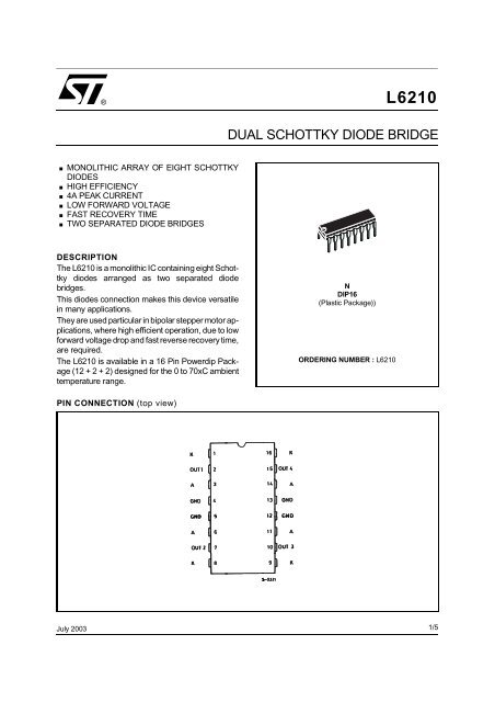
®<strong>L6210</strong>DUAL SCHOTTKY DIODE BRIDGEMONOLITHIC ARRAY OF EIGHT SCHOTTKYDIODESHIGH EFFICIENCY4A PEAK CURRENT.LOW FORWARD VOLTAGEFAST RECOVERY TIMETWO SEPARATED DIODE BRIDGESDESCRIPTIONThe <strong>L6210</strong> is a monolithic IC containing eight Schottkydiodes arranged as two separated diodebridges.This diodes connection makes this device versatilein many applications.They are used particular in bipolar stepper motor applications,where high efficient operation, due to lowforward voltage drop and fast reverse recovery time,are required.The <strong>L6210</strong> is available in a 16 Pin Powerdip Package(12 + 2 + 2) designed for the 0 to 70xC ambienttemperature range.NDIP16(Plastic Package))ORDERING NUMBER : <strong>L6210</strong>PIN CONNECTION (top view)July 20031/5
<strong>L6210</strong>BLOCK DIAGRAMABSOLUTE MAXIMUM RATINGSSymbol Parameter Value UnitI f Repetitive Forward Current Peak 2 AV r Peak Reverse Voltage (per diode) 50 VT amb Operating Ambient Temperature 70T stg Storage Temperature Range –55 to +150o Co CTHERMAL DATASymbol Parameter Value UnitR th j-case Thermal Impedance Junction-case Max. 14o C/WR th j-amb Thermal Impedance Junction-ambient without External Heatsink Max. 65o C/WELECTRICAL CHARACTERISTICS (Tj = 25 o C unless otherwise specified)Symbol Parameter Test Conditions Min. Typ. Max. UnitV f Forward Voltage Drop I f = 100 mA 0.65 0.8i f = 500 mA 0.8 1 VI f = 1 A 1 1.2I L Leakage Current V R = 40 V, T amb = 25 o C 1 mANote : At forward currents of greater than 1A, a parasitic current of approximately 10mA may be collected by adiacent diodes.2/5
<strong>L6210</strong>Figure 1 : Reverse Current verus VoltageFigure 2 : Forward Voltage versus CurrentMOUNTING INSTRUCTIONSThe Rth j-amb of the <strong>L6210</strong> can be reduced by solderingthe GND pins to suitable copper area of theprinted circuit boards as shown in figure 3 or to anexternal heatsink (figure 4). During soldering the pinFigure 3 : Example of P.C. Board Copper Areawhich is used as Heatsinktemperature must not exceed 260 o C and the solderingtime must not be longer then 12s. The externalheatsink or printed circuit copper area must be connectedto electrical ground.Figure 4 : Example of an External Heatsink3/5
<strong>L6210</strong>DIM.mminchMIN. TYP. MAX. MIN. TYP. MAX.OUTLINE ANDMECHANICAL DATAa1 0.51 0.020B 0.85 1.40 0.033 0.055b 0.50 0.020b1 0.38 0.50 0.015 0.020D 20.0 0.787E 8.80 0.346e 2.54 0.100e3 17.78 0.700F 7.10 0.280I 5.10 0.201L 3.30 0.130Z 1.27 0.050Powerdip 164/5
<strong>L6210</strong>Information furnished is believed to be accurate and reliable. However, STMicroelectronics assumes no responsibility for the consequencesof use of such information nor for any infringement of patents or other rights of third parties which may result from its use. Nolicense is granted by implication or otherwise under any patent or patent rights of STMicroelectronics. Specification mentioned in thispublication are subject to change without notice. This publication supersedes and replaces all information previously supplied. STMicroelectronicsproducts are not authorized for use as critical components in life support devices or systems without express writtenapproval of STMicroelectronics.The ST logo is a registered trademark of STMicroelectronics© 2003 STMicroelectronics – Printed in Italy – All Rights ReservedSTMicroelectronics GROUP OF COMPANIESAustralia - Brazil - Canada - China - Finland - France - Germany - Hong Kong - India - Israel - Italy - Japan - Malaysia - Malta - Morocco -Singapore - Spain - Sweden - Switzerland - United Kingdom - United States.http://www.st.com5/5