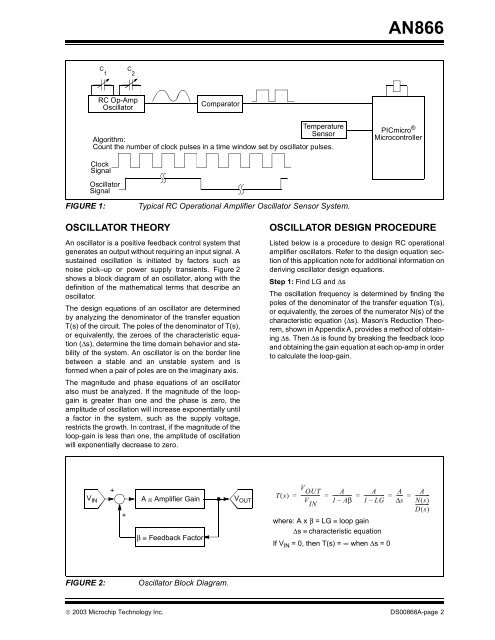
AN866Step 2: Solve N(s) = 0The second step in the procedure determines thezeroes of N(s). Routh’s stability criterion, shown inAppendix B, provides a method that determines thezeroes of the characteristic equation without thenecessity of factoring the equation.First, the Routh test consists of <strong>for</strong>ming a coefficientarray from N(s). Next, the procedure substitutes s = jω ο<strong>for</strong> s, with the summation of the row set to zero. If therow equation produces a non-trivial solution <strong>for</strong> ω ο , theprocedure is complete and the frequency of oscillationis equal to ω ο . If the row equation does not yield anequation that can be solved <strong>for</strong> ω ο , the procedure continueswith the next row in the Routh array. Usually, it isnecessary only to complete the first two or three rowsof the Routh array to produce an equation that can besolved <strong>for</strong> ω ο .Step 3: Sub-Circuit Design EquationsThe third step in the design procedure analyzes thesub-circuits <strong>for</strong>med at each amplifier. The sub-circuitequations are <strong>for</strong>med by obtaining the gain equationand pole/zero locations <strong>for</strong> each amplifier.Step 4: Verify⏐LG⏐ ≥ 1The final step in the procedure verifies that the loopgainis equal to, or greater than, one after the R and Ccomponent values have been chosen. This step is alsorequired to verify that the amplifiers do not saturate,which will result in an error in the oscillation frequency.AMPLIFIER SELECTION CRITERIAThe appropriate op amp to use in a sensor oscillator isdetermined by the required accuracy and acceptabledistortion of the oscillation frequency. The design equationsassume that the amplifiers are ideal. However, opamps have a finite gain bandwidth product (GBW), alimited slew rate (SR) and full power bandwidth (f P ).The non-ideal characteristics of the amplifier will lowerthe oscillation frequency at high frequencies and mayalso result in a design with poor start-up characteristics.Note that the total harmonic distortion specificationof the amplifiers is critical <strong>for</strong> oscillators that are usedas sine wave references. However, the shape of thewave<strong>for</strong>m is not critical in most sensor applicationsbecause only the frequency of the output is measured.Several general design rules can be used to select anop amp <strong>for</strong> an oscillator circuit. First, the GBW shouldbe a factor of 10 to 100 higher than the maximum oscillationfrequency. Next, the full-power bandwidth,defined as f P = SR / (2πV P ), where V P is the voltageswing (V O(max) - V O(min) ) of the output signal, should beat least 2 times greater than the maximum oscillationfrequency. For example, the MCP6024 quad amplifierhas a GBW = 10 MHz (typ.), SR = 7 V/µs (typ.) and a f Pof 400 kHz, with V DD = 5V. An oscillator with amaximum frequency of 100 kHz can be implementedwith the MCP6024 with enough design margin that thenon-ideal characteristics of the amplifier can beneglected.ABSOLUTE STATE-VARIABLEOSCILLATORCircuit DescriptionThe schematic of the absolute circuit is shown inFigure 3. The state-variable oscillator consists of twointegrators and an inverter circuit. Each integrator providesa phase shift of 90°, while the inverter adds anadditional 180° phase shift. The total phase shift of360° of the feedback loop produced by the three amplifiersresults in the oscillation. The first integrator stageconsists of amplifier A 1 , resistor R 1 and sensor capacitanceC 1 . The second integrator consists of amplifierA 2 , resistor R 2 and sensor capacitance C 2 . The inverterstage consists of amplifier A 3 , resistors R 3 and R 4 andcapacitor C 4 . The addition of capacitor C 4 helps ensureoscillation start-up by providing an additional phaseshift.The absolute oscillator does not require a limit circuit ifrail-to-rail input/output (RRIO) amplifiers are used andthe gain of the inverter stage (A 3 ) is equal to one(i.e., R 3 = R 4 ). The sinewave output of the signal willswing within approximately 50 mV of the V DD and V DDpower rails as shown in Figure 5.A complementary output voltage comparator (A 4 ) isused to convert the oscillator’s sinewave output to asquare wave digital signal. The comparator functionsas a zero-crossing detector and the switching point isequal to the virtual ground voltage (i.e., V DD /2). ResistorR 9 is used to provide additional hysteresis (V HYS ) tothe comparator. Listed below is the hysteresisequation.EQUATION:RV = -------------------- 8× ( V – V )HYS R 8+ R Omax ( ) Omin ( )9R 8V HYS≅ -------------------- × VR 8+ R DD 9© 2003 <strong>Microchip</strong> Technology Inc. DS00866A-page 3