Semiconductors: Arrhenius plot of - Wits Structural Chemistry
Semiconductors: Arrhenius plot of - Wits Structural Chemistry
Semiconductors: Arrhenius plot of - Wits Structural Chemistry
- No tags were found...

You also want an ePaper? Increase the reach of your titles
YUMPU automatically turns print PDFs into web optimized ePapers that Google loves.
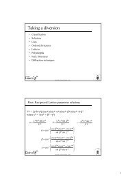
<strong>Semiconductors</strong>• Conductivity (σ)() increases (exponentially)with temperature; compare to metals<strong>Semiconductors</strong>• Calculate the fraction <strong>of</strong> Si atoms thatprovide a conduction e - at roomtemperature and compare this to thevalue obtained for Cu.• [density (Si) = 2.33g/cm 3 ; M(Si) ) = 28.09 g/mol; carrier density n e =14 x 10 15 m - 3 ]• Ans: : fraction = 2.8 x 10 -13cf 1.23• Exercise: convert 1eV and 6eV to kJ/mol<strong>Semiconductors</strong>:change in the Fermi function (f(E((E) with temperature1f ( E)=[exp( E − E ) / kT]+ 1F<strong>Semiconductors</strong>1f ( E)=[exp( E − E ) / kT]+ 1Calculate the probability <strong>of</strong> an e - beingthermally promoted to the conductionband <strong>of</strong> Si (E(g = 1.07eV) at 25 °CFAns: f(E) ) = 4.39 x 10 -10<strong>Semiconductors</strong>Band gaps, E g (eV)<strong>Semiconductors</strong>: <strong>Arrhenius</strong> <strong>plot</strong><strong>of</strong> electrical conductivity• conductivity is proportional to the density <strong>of</strong> charge carrierssinceandσ = nq( μ + μh)en ∝ exp( −Eg/ 2kT)from f(E)E g 1∴ln( σ ) = ln( σ0)−2kT1
<strong>Semiconductors</strong>: <strong>Arrhenius</strong> <strong>plot</strong><strong>of</strong> electrical conductivityE g 1∴ln( σ ) = ln( σ0)−2kT• Note: althoughconductivity will decreaseas T increases in allmaterials due to thermalvibration, but this is onlysignificant in metals• see example<strong>Semiconductors</strong>To characterize a new semiconductor one can find theband gap by measuring conductivity at differenttemperatures (Note: this can also be donespectroscopically).Example: The conductivity <strong>of</strong> a new material is 250Ω -1 m -1 at 20°C C and at 100°C C it is 1100 Ω -1 m -1 . What isits band gap, E g ?Ans: : 0.349 eVIntrinsic semiconductors• conductivity in an intrinsic (pure) semiconductor depends on the bandgap energy and temperature.• Examples <strong>of</strong> intrinsic semiconductors are Si, Ge, , Se, GaAs, CdSIntrinsic semiconductorsrange <strong>of</strong> band gaps• electrons can also be excited into theconduction band by light <strong>of</strong> the correctenergy: E=hc/hc/λ. . Conversely, light can beemitted (tunable(LED’s).• Ex: Calculate the photon wavelength (nm)needed to promote an e - to the conductionband in Si.p- and n-doped nsemiconductors• small amounts <strong>of</strong> dopants (from 0.01 atom% to less than 1 atom in 10 9 )can be added to modify the conductivity (“extrinsic(semiconductors”)and subsequently to make electronic devices.• (see periodic table to decide on p-por n-dopants)p- and n-doped nsemiconductorsband structure• p- and n-dopantsmodify the band structure <strong>of</strong> a semiconductor;effectively adding either ‘donor’ or ‘acceptor’ bands.p-dopant2
p- and n-doped nsemiconductors:band structure• n-dopantExtrinsic semiconductors• Extrinsic semiconductors exhibit an ‘exhaustion range’ at a certaintemperature when all “extra electrons” have been promoted to theconduction band.The p-n p n junction• The p-n juction is one <strong>of</strong> the simplest and most common applicationsusing semiconductors in a variety <strong>of</strong> devices (transistors, siliconchips, photocells, LED’s,thermistors)Current flow in a p-n p n junction• The p-n junction acts as a solid-state state rectifier, allowing current t<strong>of</strong>low only in one direction• Nano-CdSeCdSe: : optical properties vary withparticle sizeRadius (nm)0.9 1.4 1.9 2.4• Nano-CdSeCdSe: : synthesis by organometallicmethods3
• Nano-CdSesemiconductorInsulators• Band gaps; range <strong>of</strong> conductivity; examplesInsulators• Piezoelectric and pyroelectric effects(see text books: AR West)Insulators• Barium titanate structure and the Piezoelectric effect(see text books)Insulators• Other perovskite structures (solid solutions)Electrical properties <strong>of</strong> solids:Summary• Conductors can be classified according to their response to temperature:erature:conductors, semiconductors & superconductors.• The electronic properties <strong>of</strong> solids can be rationalised using band theory• For metallic conductors, resistivity is proportional to temperature.• For semiconductors, conductivity increases exponentially withtemperature. The population <strong>of</strong> the conduction band as a function <strong>of</strong>temperature is given by the Fermic-Dirac distribution.• Radiation <strong>of</strong> the correct energy can also excite electrons into the tconduction band. Conversely light <strong>of</strong> different wavelengths (Eg(Eg) ) can beemitted.• Extrinsic semiconductors have a higher conductivity than similar intrinsicones at low temperature.• The conductivity <strong>of</strong> extrinsic semiconductors is accurately controlled olled bythe concentration <strong>of</strong> the dopant; ; wide temperature range possible.• Superconductivity phenomena can be explained in terms <strong>of</strong> ‘Cooper pairs<strong>of</strong> electrons’, , which can conduct electricity with zero resistance4