Si4707-B20 - Silicon Labs
Si4707-B20 - Silicon Labs
Si4707-B20 - Silicon Labs
- No tags were found...

You also want an ePaper? Increase the reach of your titles
YUMPU automatically turns print PDFs into web optimized ePapers that Google loves.
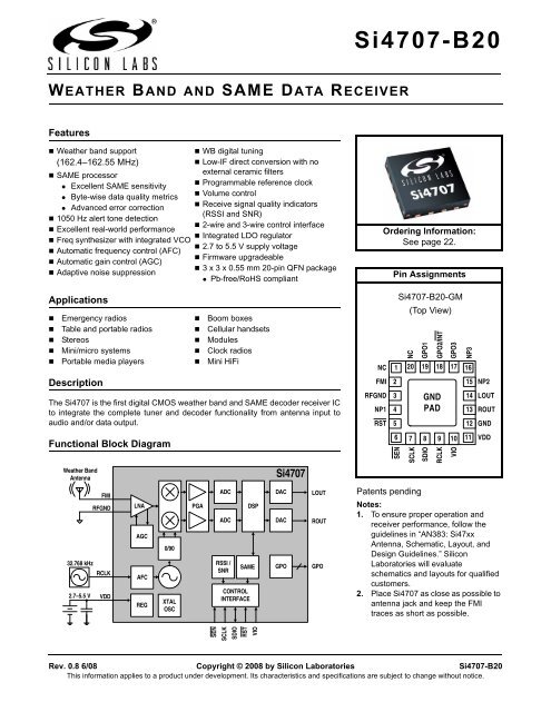
<strong>Si4707</strong>-<strong>B20</strong>WEATHER BAND AND SAME DATA RECEIVERFeatures• Weather band support(162.4–162.55 MHz)• SAME processor•Excellent SAME sensitivity•Byte-wise data quality metrics•Advanced error correction• 1050 Hz alert tone detection• Excellent real-world performance• Freq synthesizer with integrated VCO• Automatic frequency control (AFC)• Automatic gain control (AGC)• Adaptive noise suppression• WB digital tuning• Low-IF direct conversion with noexternal ceramic filters• Programmable reference clock• Volume control• Receive signal quality indicators(RSSI and SNR)• 2-wire and 3-wire control interface• Integrated LDO regulator• 2.7 to 5.5 V supply voltage• Firmware upgradeable• 3 x 3 x 0.55 mm 20-pin QFN package• Pb-free/RoHS compliantOrdering Information:See page 22.Pin AssignmentsApplications• Emergency radios• Table and portable radios• Stereos• Mini/micro systems• Portable media players• Boom boxes• Cellular handsets• Modules• Clock radios• Mini HiFiNC1<strong>Si4707</strong>-<strong>B20</strong>-GM(Top View)NC20GPO119GPO2/INTGPO31817NP316DescriptionFMI215NP2The <strong>Si4707</strong> is the first digital CMOS weather band and SAME decoder receiver ICto integrate the complete tuner and decoder functionality from antenna input toaudio and/or data output.RFGNDNP1RST345GNDPAD141312LOUTROUTGNDFunctional Block Diagram6 7 8 91011Weather BandAntenna<strong>Si4707</strong>32.768 kHz2.7–5.5 VFMIRFGNDRCLKVDDLNAAGCAFCREG0/90XTALOSCPGAADCADCRSSI /SNRCONTROLINTERFACEDSPSAMEDACDACGPOLOUTROUTGPOPatents pendingNotes:1. To ensure proper operation andreceiver performance, follow theguidelines in “AN383: Si47xxAntenna, Schematic, Layout, andDesign Guidelines.” <strong>Silicon</strong>Laboratories will evaluateschematics and layouts for qualifiedcustomers.2. Place <strong>Si4707</strong> as close as possible toantenna jack and keep the FMItraces as short as possible.SENSCLKSDIORSTVIOSENSCLKSDIORCLKVIOVDDRev. 0.8 6/08 Copyright © 2008 by <strong>Silicon</strong> Laboratories <strong>Si4707</strong>-<strong>B20</strong>This information applies to a product under development. Its characteristics and specifications are subject to change without notice.
<strong>Si4707</strong>-<strong>B20</strong>2 Rev. 0.8
<strong>Si4707</strong>-<strong>B20</strong>TABLE OF CONTENTSSectionPage1. Electrical Specifications . . . . . . . . . . . . . . . . . . . . . . . . . . . . . . . . . . . . . . . . . . . . . . . . . . .42. Typical Application Schematic . . . . . . . . . . . . . . . . . . . . . . . . . . . . . . . . . . . . . . . . . . . . .123. Bill of Materials . . . . . . . . . . . . . . . . . . . . . . . . . . . . . . . . . . . . . . . . . . . . . . . . . . . . . . . . . .134. Functional Description . . . . . . . . . . . . . . . . . . . . . . . . . . . . . . . . . . . . . . . . . . . . . . . . . . .144.1. Overview . . . . . . . . . . . . . . . . . . . . . . . . . . . . . . . . . . . . . . . . . . . . . . . . . . . . . . . . . .144.2. Block Diagram Description . . . . . . . . . . . . . . . . . . . . . . . . . . . . . . . . . . . . . . . . . . . .154.3. Weather Band Receiver . . . . . . . . . . . . . . . . . . . . . . . . . . . . . . . . . . . . . . . . . . . . . .154.4. DAC . . . . . . . . . . . . . . . . . . . . . . . . . . . . . . . . . . . . . . . . . . . . . . . . . . . . . . . . . . . . . .154.5. SAME Processor . . . . . . . . . . . . . . . . . . . . . . . . . . . . . . . . . . . . . . . . . . . . . . . . . . . .154.6. Tuning . . . . . . . . . . . . . . . . . . . . . . . . . . . . . . . . . . . . . . . . . . . . . . . . . . . . . . . . . . . .164.7. Reference Clock . . . . . . . . . . . . . . . . . . . . . . . . . . . . . . . . . . . . . . . . . . . . . . . . . . . .164.8. Control Interface . . . . . . . . . . . . . . . . . . . . . . . . . . . . . . . . . . . . . . . . . . . . . . . . . . . .164.9. GPO Outputs . . . . . . . . . . . . . . . . . . . . . . . . . . . . . . . . . . . . . . . . . . . . . . . . . . . . . . .184.10. Firmware Upgrades . . . . . . . . . . . . . . . . . . . . . . . . . . . . . . . . . . . . . . . . . . . . . . . . .184.11. Reset, Powerup, and Powerdown . . . . . . . . . . . . . . . . . . . . . . . . . . . . . . . . . . . . . .184.12. Programming with Commands . . . . . . . . . . . . . . . . . . . . . . . . . . . . . . . . . . . . . . . .185. Commands and Properties . . . . . . . . . . . . . . . . . . . . . . . . . . . . . . . . . . . . . . . . . . . . . . . .196. Pin Descriptions: <strong>Si4707</strong>-<strong>B20</strong> . . . . . . . . . . . . . . . . . . . . . . . . . . . . . . . . . . . . . . . . . . . . . .217. Ordering Guide . . . . . . . . . . . . . . . . . . . . . . . . . . . . . . . . . . . . . . . . . . . . . . . . . . . . . . . . . .228. Package Markings (Top Marks) . . . . . . . . . . . . . . . . . . . . . . . . . . . . . . . . . . . . . . . . . . . . .238.1. Top Mark . . . . . . . . . . . . . . . . . . . . . . . . . . . . . . . . . . . . . . . . . . . . . . . . . . . . . . . . . .238.2. Top Mark Explanation . . . . . . . . . . . . . . . . . . . . . . . . . . . . . . . . . . . . . . . . . . . . . . . .239. Package Outline: <strong>Si4707</strong> QFN . . . . . . . . . . . . . . . . . . . . . . . . . . . . . . . . . . . . . . . . . . . . . .2410. PCB Land Pattern: <strong>Si4707</strong> QFN . . . . . . . . . . . . . . . . . . . . . . . . . . . . . . . . . . . . . . . . . . . .2511. Additional Reference Resources . . . . . . . . . . . . . . . . . . . . . . . . . . . . . . . . . . . . . . . . . .27Document Change List . . . . . . . . . . . . . . . . . . . . . . . . . . . . . . . . . . . . . . . . . . . . . . . . . . . . .28Contact Information . . . . . . . . . . . . . . . . . . . . . . . . . . . . . . . . . . . . . . . . . . . . . . . . . . . . . . . .30Rev. 0.8 3
<strong>Si4707</strong>-<strong>B20</strong>1. Electrical SpecificationsTable 1. Recommended Operating ConditionsParameter Symbol Test Condition Min Typ Max UnitSupply Voltage V DD 2.7 — 5.5 VInterface Supply Voltage V IO 1.5 — 3.6 VPower Supply Powerup Rise Time V DDRISE 10 — — µsInterface Power Supply Powerup Rise Time V IORISE 10 — — µsAmbient Temperature T A –20 25 85 CNote: All minimum and maximum specifications are guaranteed and apply across the recommended operating conditions.Typical values apply at VDD = 3.3 V and 25 C unless otherwise stated. Parameters are tested in production unlessotherwise stated.Table 2. Absolute Maximum Ratings 1,2Parameter Symbol Value UnitSupply Voltage V DD –0.5 to 5.8 VInterface Supply Voltage V IO –0.5 to 3.9 VInput Current 3 I IN 10 mAInput Voltage 3 V IN –0.3 to (VIO + 0.3) VOperating Temperature T OP –40 to 95 CStorage Temperature T STG –55 to 150 CRF Input Level 4 0.4 V pKNotes:1. Permanent device damage may occur if the above Absolute Maximum Ratings are exceeded. Functional operationshould be restricted to the conditions as specified in the operational sections of this data sheet. Exposure beyondrecommended operating conditions for extended periods may affect device reliability.2. The <strong>Si4707</strong> devices are high-performance RF integrated circuits with certain pins having an ESD rating of < 2 kV HBM.Handling and assembly of these devices should only be done at ESD-protected workstations.3. For input pins SCLK, SEN, SDIO, RST, RCLK, GPO1, GPO2, and GPO3.4. At RF input pins, FMI.4 Rev. 0.8
<strong>Si4707</strong>-<strong>B20</strong>Table 3. DC Characteristics(V DD = 2.7 to 5.5 V, V IO = 1.5 to 3.6 V, T A = –20 to 85 C)Parameter Symbol Test Condition Min Typ Max UnitSupply Current I FM — 19.1 23 mAInterface Supply Current I IO — 320 600 µAV DD Powerdown Current 1 I DDPD — 10 20 µAV IO Powerdown Current 1 I IOPD SCLK, RCLK inactive — 1 10 µAHigh Level Input Voltage 2 V IH 0.7 x VIO — — VLow Level Input Voltage 2 V IL — — 0.3 x VIO VHigh Level Input Current 2 I IH V IN = VIO = 3.6 V –10 — 10 µALow Level Input Current 2 I IL V IN =0V,V IO =3.6V–10 — 10 µAHigh Level Output Voltage 3 V OH I OUT = 500 µA 0.8 x VIO — — VLow Level Output Voltage 3 V OL I OUT = –500 µA — — 0.2 x VIO VNotes:1. Specifications are guaranteed by characterization.2. For input pins SCLK, SEN, SDIO, RST, and RCLK.3. For output pins SDIO, GPO1, GPO2, and GPO3.Rev. 0.8 5
<strong>Si4707</strong>-<strong>B20</strong>Table 4. Reset Timing Characteristics 1,2,3(V DD = 2.7 to 5.5 V, V IO = 1.5 to 3.6 V, T A = –20 to 85 °C)Parameter Symbol Min Typ Max UnitRST Pulse Width and GPO1, GPO2/INT Setup to RST t SRST 100 — — µsGPO1, GPO2/INT Hold from RST t HRST 30 — — nsNotes:1. When selecting 2-wire mode, the user must ensure that a 2-wire start condition (falling edge of SDIO while SCLK ishigh) does not occur within 300 ns before the rising edge of RST.2. When selecting 2-wire mode, the user must ensure that SCLK is high during the rising edge of RST, and stays high untilafter the first start condition.3. When selecting 3-wire or SPI modes, the user must ensure that a rising edge of SCLK does not occur within 300 nsbefore the rising edge of RST.4. If GPO1 and GPO2 are actively driven by the user, then minimum t SRST is only 30 ns. If GPO1 or GPO2 is hi-Z, thenminimum t SRST is 100 µs to provide time for on-chip 1 M devices (active while RST is low) to pull GPO1 high andGPO2 low.t SRSTt HRSTRST70%30%GPO1 70%30%GPO2/INT70%30%Figure 1. Reset Timing Parameters for Busmode Select6 Rev. 0.8
<strong>Si4707</strong>-<strong>B20</strong>Table 5. 2-Wire Control Interface Characteristics 1,2,3(V DD = 2.7 to 5.5 V, V IO = 1.5 to 3.6 V, T A = –20 to 85 °C)Parameter Symbol Test Condition Min Typ Max UnitSCLK Frequency f SCL 0 — 400 kHzSCLK Low Time t LOW 1.3 — — µsSCLK High Time t HIGH 0.6 — — µsSCLK Input to SDIO Setup t SU:STA 0.6 — — µs(START)SCLK Input to SDIO Holdt HD:STA 0.6 — — µs(START)SDIO Input to SCLK Setup t SU:DAT 100 — — nsSDIO Input to SCLK Hold 4,5 t HD:DAT 0 — 900 nsSCLK input to SDIO Setup t SU:STO 0.6 — — µs(STOP)STOP to START Time t BUF 1.3 — — µsSDIO Output Fall Time t f:OUT — 250 ns20 0.1 C b+ ----------1pFSDIO Input, SCLK Rise/Fall Timet f:IN— 300 nst r:IN20 0.1 C b+ ----------1pFSCLK, SDIO Capacitive Loading C b — — 50 pFInput Filter Pulse Suppression t SP — — 50 nsNotes:1. When V IO = 0 V, SCLK and SDIO are low impedance.2. When selecting 2-wire mode, the user must ensure that a 2-wire start condition (falling edge of SDIO while SCLK ishigh) does not occur within 300 ns before the rising edge of RST.3. When selecting 2-wire mode, the user must ensure that SCLK is high during the rising edge of RST, and stays highuntil after the first start condition.4. The <strong>Si4707</strong> delays SDIO by a minimum of 300 ns from the V IH threshold of SCLK to comply with the minimum t HD:DATspecification.5. The maximum t HD:DAT has only to be met when f SCL = 400 kHz. At frequencies below 400 kHz, t HD:DAT may be violatedas long as all other timing parameters are met.Rev. 0.8 7
<strong>Si4707</strong>-<strong>B20</strong>t SU:STA t HD:STAt LOWt HIGHt r:INt f:INt SPtSU:STOt BUFSCLK 70%30%SDIO 70%30%STARTt r:INt HD:DAT t SU:DATt f:IN,t f:OUTSTOPSTARTFigure 2. 2-Wire Control Interface Read and Write Timing ParametersSCLKSDIOA6-A0,R/WD7-D0D7-D0STARTADDRESS + R/W ACK DATA ACK DATA ACKFigure 3. 2-Wire Control Interface Read and Write Timing DiagramSTOP8 Rev. 0.8
<strong>Si4707</strong>-<strong>B20</strong>Table 6. 3-Wire Control Interface Characteristics(V DD = 2.7 to 5.5 V, V IO = 1.5 to 3.6 V, T A = –20 to 85 °C)Parameter Symbol Test Condition Min Typ Max UnitSCLK Frequency f CLK 0 — 2.5 MHzSCLK High Time t HIGH 25 — — nsSCLK Low Time t LOW 25 — — nsSDIO Input, SEN to SCLKSetup t S 20 — — nsSDIO Input to SCLKHold t HSDIO 10 — — nsSEN Input to SCLKHold t HSEN 10 — — nsSCLKto SDIO Output Valid t CDV Read 2 — 25 nsSCLKto SDIO Output High Z t CDZ Read 2 — 25 nsSCLK, SEN, SDIO, Rise/Fall Time t R , t F — — 10 nsNote: When selecting 3-wire mode, the user must ensure that a rising edge of SCLK does not occur within 300 ns before therising edge of RST.SCLK 70%30%t R t F½ Cycle BusSEN 70%30%t HIGHt St St HSDIO t HSENt LOW70%A6-A5,SDIO A7 R/W, A030%A4-A1D15 D14-D1 D0Address InData InFigure 4. 3-Wire Control Interface Write Timing ParametersSCLK 70%30%SEN 70%30%t St St HSDIO t CDV t HSENt CDZSDIO70%30%A7A6-A5,R/W,A4-A1A0D15 D14-D1 D0Address InData OutTurnaroundFigure 5. 3-Wire Control Interface Read Timing ParametersRev. 0.8 9
<strong>Si4707</strong>-<strong>B20</strong>Table 7. SPI Control Interface Characteristics(V DD = 2.7 to 5.5 V, V IO = 1.5 to 3.6 V, T A = –20 to 85 °C)Parameter Symbol Test Condition Min Typ Max UnitSCLK Frequency f CLK 0 — 2.5 MHzSCLK High Time t HIGH 25 — — nsSCLK Low Time t LOW 25 — — nsSDIO Input, SEN to SCLKSetup t S 15 — — nsSDIO Input to SCLKHold t HSDIO 10 — — nsSEN Input to SCLKHold t HSEN 5 — — nsSCLKto SDIO Output Valid t CDV Read 2 — 25 nsSCLKto SDIO Output High Z t CDZ Read 2 — 25 nsSCLK, SEN, SDIO, Rise/Fall Time t R , t F — — 10 nsNote: When selecting SPI mode, the user must ensure that a rising edge of SCLK does not occur within 300 ns before therising edge of RST.SCLK 70%30%t Rt FSEN 70%30%t St St HIGH t LOW t HSDIOt HSEN70%SDIO C7 C6–C1 C030%D7 D6–D1 D0Control Byte In8 Data Bytes InFigure 6. SPI Control Interface Write Timing ParametersSCLK 70%30%t CDVSEN 70%30%t St St HSDIOtHSENt CDZSDIO 70%30%C7C6–C1C0D7 D6–D1 D0Control Byte InBusTurnaround16 Data Bytes Out(SDIO or GPO1)Figure 7. SPI Control Interface Read Timing Parameters10 Rev. 0.8
<strong>Si4707</strong>-<strong>B20</strong>Table 8. WB Receiver Characteristics 1(V DD = 2.7 to 5.5 V, V IO = 1.5 to 3.6V, T A = 25 °C)Parameter Symbol Test Condition Min Typ Max UnitInput Frequency f R 162.4 — 162.55 MHzSensitivity 2,3,4 SINAD = 12 dB — 0.45 — µV EMFAdjacent Channel Selectivity ±25 kHz — 55 — dBAudio S/N 2,3,4,5 — 45 — dBAudio Frequency Reponse Low –3 dB — — 300 HzAudio Frequency Reponse High –3 dB 3 — — kHzAFSK Trip Sensitivity 6100% of message — 0.45 — µV EMFcorrectly receivedNotes:1. To ensure proper operation and receiver performance, follow the guidelines in “AN383: Si47xx Antenna, Schematic,Layout, and Design Guidelines.” <strong>Silicon</strong> Laboratories will evaluate schematics and layouts for qualified customers.2. F MOD = 1 kHz.3. f = 3 kHz.4. B AF = 300 Hz to 15 kHz, A-weighted.5. V EMF =1mV.6. f = 4 kHz.Table 9. Reference Clock and Crystal Characteristics(V DD = 2.7 to 5.5 V, V IO = 1.5 to 3.6 V, T A = –20 to 85 °C)Parameter Symbol Test Condition Min Typ Max UnitReference ClockRCLK Supported Frequency * 31.130 32.768 40,000.0 kHzRCLK Frequency Tolerance –50 — 50 ppmREFCLK_PRESCALE 1 — 4095REFCLK 31.130 32.768 34.406 kHzCrystal OscillatorCrystal Oscillator Frequency — 32.768 — kHzCrystal Frequency Tolerance –50 — 50 ppmBoard Capacitance — — 3.5 pF*Note: The <strong>Si4707</strong> divides the RCLK input by REFCLK_PRESCALE to obtain REFCLK. There are some RCLK frequenciesbetween 31.130 kHz and 40 MHz that are not supported. See AN332, Table 6 for more details.Rev. 0.8 11
<strong>Si4707</strong>-<strong>B20</strong>2. Typical Application SchematicGPO1GPO2GPO3NCGPO1GPO2GPO3NP32019181716FMI12345NCFMIRFGNDNP1RSTU1<strong>Si4707</strong>-GMSENSCLKSDIORCLKVIONP2LOUTROUTGNDVDD1514131211LOUTROUTC1VBATTERY2.7 to 5.5 VRSTSENSCLKSDIORCLKVIO1.5 to 3.6 V678910X1GPO3RCLKC2 C3Optional: for crystal oscillator optionNotes:1. Place C1 close to V DD pin.2. All grounds connect directly to GND plane on PCB.3. Pins 1 and 20 are no connects, leave floating.4. Pins 4, 15, and 16 are unused; recommend connecting to ground.5. To ensure proper operation and receiver performance, follow the guidelines in “AN383: Si47xx Antenna, Schematic,Layout, and Design Guidelines.” <strong>Silicon</strong> Laboratories will evaluate schematics and layouts for qualified customers.6. Pin 2 connects to the WB antenna interface.7. Place <strong>Si4707</strong> as close as possible to antenna jack and keep the FMI trace as short as possible.12 Rev. 0.8
<strong>Si4707</strong>-<strong>B20</strong>3. Bill of MaterialsComponent(s) Value/Description SupplierC1 Supply bypass capacitor, 22 nF, ±20%, Z5U/X7R MurataU1 <strong>Si4707</strong> WB + SAME Receiver <strong>Silicon</strong> LaboratoriesOptional ComponentsC2, C3 Crystal load capacitors, 22 pF, ±5%, COGVenkel(Optional: for crystal oscillator option)X1 32.768 kHz crystal (Optional: for crystal oscillator option) EpsonRev. 0.8 13
<strong>Si4707</strong>-<strong>B20</strong>4. Functional Description4.1. OverviewWeather BandAntenna<strong>Si4707</strong>FMIADCDACLOUTRFGNDLNAPGADSPADCDACROUTAGC0/9032.768 kHzRCLKAFCRSSI /SNRSAMEGPOGPO2.7–5.5 VVDDREGXTALOSCCONTROLINTERFACEThe <strong>Si4707</strong> is the industry's first weather band (WB)radio receiver IC to include a specific area messageencoding (SAME) processor. Offering unmatchedintegration and PCB space savings, the <strong>Si4707</strong> requiresonly one external component and less than 15 mm 2 ofboard area. Available in a tiny 3 x 3 mm QFN package,it eliminates the need for a front-end tuner IC, externalADC, DSP processor, RAM, and numerous discretecomponents found in traditional SAME weather bandradios. The <strong>Si4707</strong> weather band receiver provides thespace savings and low power consumption necessaryfor portable devices while delivering the highperformance and design simplicity desired for allweather alert radios.Leveraging <strong>Silicon</strong> Laboratories' proven and patentedSi4700/01 FM tuner's digital low intermediate frequency(low-IF) receiver architecture, the <strong>Si4707</strong> deliverssuperior RF performance combined with sophisticateddigital processing to yield best-in-class audio qualityand SAME data sensitivity.SENSCLKSDIORSTVIOFigure 8. Functional Block DiagramThe high integration and complete system productiontest simplifies design in, increases system quality, andimproves manufacturability.The <strong>Si4707</strong> is a feature-rich solution including 1050 Hztone detection, automatic frequency control, dynamicchannel bandwidth filters, and digital tuning. In addition,the <strong>Si4707</strong> provides a programmable reference clockand supports an I 2 C compatible 2-wire control interface,SPI, and a Si4700/01 backwards compatible 3-wirecontrol interface.The <strong>Si4707</strong> incorporates a digital processor to provideSAME data, advance error correction, and SAME dataquality metrics. Using this feature, the <strong>Si4707</strong> enablesbroadcast alert data such as severe thunderstormwarning or flash flood watch to be displayed to the user.14 Rev. 0.8
<strong>Si4707</strong>-<strong>B20</strong>4.2. Block Diagram DescriptionThe <strong>Si4707</strong> IC integrates the voltage-controlledoscillator (VCO) and frequency synthesizer and acceptsa wide-range of programmable reference clocks(RCLK). The IC also supports a dedicated externalcrystal with an integrated crystal oscillator. Thefrequency synthesizer generates the quadrature localoscillator signal used to downconvert the RF input to alow intermediate frequency. The VCO frequency islocked to the RCLK and adjusted with an automaticfrequency control (AFC) servo loop during reception.The VCO frequency is modified according to the targetfrequency and varies according to the tuned channel.The <strong>Si4707</strong> uses a digital low-IF architecture,integrating the entire analog receive chain for WB. TheIC also integrates the functionality of most externalcomponents typically found in competing solutions andperforms all processing in an on-chip digital signalprocessor (DSP) and microcontroller (MCU) core. Theanalog chain includes a dedicated low-noise amplifier(LNA), automatic gain control (AGC), image-rejectquadrature mixer, programmable gain amplifier (PGA),and a set of delta-sigma high-performance ADCs. TheLNA block receives wide-band frequency input at theFMI input pin. The on-chip resistor blocks control thegain of the external WB antenna network. The LNA gainis dynamically controlled by the AGC loop, contingenton the RF peak detectors and signal strength. Thereceive path continues to dedicated quadrature mixersthat downconvert the received signal from RF to low-IF,filter for out-of-band interferers, and perform a transferfunction to shift the tuned frequency to DC. A single pairof PGAs filters the multiplexed (MPX) mixer output frominterferers and amplifies the signal again beforedelivering it to two high-resolution analog-to-digitalconverters (ADC). The digital core performs channelselection and filtering, digital calibrated tuning, FMdemodulation, and SAME demodulation/decoding. Thecore also performs signal quality processing includingreceived signal strength indicators (RSSI) and SNR.4.3. Weather Band ReceiverThe <strong>Si4707</strong> supports weather band reception from162.4 to 162.55 MHz. The highly-integrated <strong>Si4707</strong>meets NOAA and Weather Radio Canadaspecifications, receives all seven specified frequencies,implements narrow-band FM de-emphasis, andsupports 1050 Hz alert tone detection. In addition, the<strong>Si4707</strong> provides advanced features not available onconventional radios, such as an AFC, a dynamicchannel bandwidth filter, and RSSI and SNR receivesignal quality indicators.The AFC locks on to the strongest signal within anarrow, adjustable frequency range to compensate forany potential frequency errors such as crystal toleranceor transmit frequency errors. The AFC ensures thechannel filter is always centered on the desired channelproviding optimal reception. The dynamic channelbandwidth feature utilizes a wide filter in strong signalconditions to provide best sound quality and a narrowerfilter in weak conditions to provide best sensitivity.4.4. DACHigh-fidelity stereo digital-to-analog converters (DACs)drive analog audio signals onto the LOUT and ROUTpins. Weather band stations broadcast in mono only, soLOUT and ROUT audio will be the same. The audiooutput may be muted. Volume is adjusted digitally withthe RX_VOLUME property.4.5. SAME ProcessorThe <strong>Si4707</strong> implements a high-performance SAMEprocessor for demodulation, byte-wise data qualitymetrics, and advanced error correction beyond thecommonly used polling method. The SAME decoderdraws on soft decision decoding techniques to providerobust performance and delivers reception inenvironments where signal power is very low orcompromised.The <strong>Si4707</strong> device stores the entire SAME messageand provides a user programmable interrupt at the endof message detected, start of message detected,preamble detected, and/or header buffer ready. It alsoreports on the confidence level of each byte of data witha value of 0–3, with 3 representing the highestconfidence level. This feature, unique to the <strong>Si4707</strong>,provides extra visibility into the message accuracy,which helps limit the number of false messages in poorreception areas.Rev. 0.8 15
<strong>Si4707</strong>-<strong>B20</strong>4.6. TuningThe frequency synthesizer uses <strong>Silicon</strong> Laboratories’proven technology, including a completely integratedVCO. The frequency synthesizer generates thequadrature local oscillator signal used to downconvertthe RF input to a low intermediate frequency. The VCOfrequency is locked to the reference clock and adjustedwith an AFC servo loop during reception. The tuningfrequency can be directly programmed using theWB_TUNE_FREQ.4.7. Reference ClockThe <strong>Si4707</strong> reference clock is programmable,supporting RCLK frequencies in Table 9. Refer toTable 3, “DC Characteristics,” on page 5 for switchingvoltage levels and Table 8, “WB ReceiverCharacteristics 1 ,” on page 11 for frequency toleranceinformation. Using RCLK is the recommended methodin order to meet the ±50 ppm requirement.An onboard crystal oscillator is available to generate the32.768 kHz reference when an external crystal and loadcapacitors are provided. Refer to "2. Typical ApplicationSchematic" on page 12. This mode is enabled using thePOWER_UP command, see Table 11, “<strong>Si4707</strong>Command Summary,” on page 19.The <strong>Si4707</strong> performance may be affected by dataactivity on the SDIO bus when using the integratedinternal oscillator. SDIO activity results from polling thetuner for status or communicating with other devicesthat share the SDIO bus. If there is SDIO bus activitywhile the <strong>Si4707</strong> is performing the tune function, thecrystal oscillator may experience jitter, which may resultin lower SNR.4.8. Control InterfaceA serial port slave interface is provided, which allows anexternal controller to send commands to the <strong>Si4707</strong> andreceive responses from the device. The serial port canoperate in three bus modes: 2-wire mode, 3-wire mode,or SPI mode. The <strong>Si4707</strong> selects the bus mode bysampling the state of the GPO1 and GPO2 pins on therising edge of RST. The GPO1 pin includes an internalpull-up resistor, which is connected while RST is low,and the GPO2 pin includes an internal pull-downresistor, which is connected while RST is low.Therefore, it is only necessary for the user to activelydrive pins that differ from these states. See Table 10.Table 10. Bus Mode Select on Rising Edge ofRSTBus Mode GPO1 GPO22-Wire 1 0SPI 1 1 (must drive)3-Wire 0 (must drive) 0After the rising edge of RST, the pins GPO1 and GPO2are used as general purpose output (O) pins asdescribed in Section “4.9. GPO Outputs”. In any busmode, commands may only be sent after VIO and VDDsupplies are applied.In any bus mode, before sending a command or readinga response, the user must first read the status byte toensure that the device is ready (CTS bit is high).16 Rev. 0.8
<strong>Si4707</strong>-<strong>B20</strong>4.8.1. 2-Wire Control Interface ModeWhen selecting 2-wire mode, the user must ensure thatSCLK is high during the rising edge of RST, and stayshigh until after the first start condition. Also, a startcondition must not occur within 300 ns before the risingedge of RST.The 2-wire bus mode uses only the SCLK and SDIOpins for signaling. A transaction begins with the STARTcondition, which occurs when SDIO falls while SCLK ishigh. Next, the user drives an 8-bit control word seriallyon SDIO, which is captured by the device on risingedges of SCLK. The control word consists of a 7-bitdevice address, followed by a read/write bit (read = 1,write = 0). The <strong>Si4707</strong> acknowledges the control wordby driving SDIO low on the next falling edge of SCLK.Although the <strong>Si4707</strong> will respond to only a single deviceaddress, this address can be changed with the SEN pin(note that the SEN pin is not used for signaling in 2-wiremode). When SEN = 0, the 7-bit device address is0010001b. When SEN = 1, the address is 1100011b.For write operations, the user then sends an 8-bit databyte on SDIO, which is captured by the device on risingedges of SCLK. The <strong>Si4707</strong> acknowledges each databyte by driving SDIO low for one cycle, on the nextfalling edge of SCLK. The user may write up to eightdata bytes in a single 2-wire transaction. The first byte isa command, and the next seven bytes are arguments.For read operations, after the <strong>Si4707</strong> hasacknowledged the control byte, it will drive an 8-bit databyte on SDIO, changing the state of SDIO on the fallingedge of SCLK. The user acknowledges each data byteby driving SDIO low for one cycle, on the next fallingedge of SCLK. If a data byte is not acknowledged, thetransaction will end. The user may read up to 16 databytes in a single 2-wire transaction. These bytes containthe response data from the <strong>Si4707</strong>.A 2-wire transaction ends with the STOP condition,which occurs when SDIO rises while SCLK is high.For details on timing specifications and diagrams, referto Table 5, “2-Wire Control Interface Characteristics” onpage 7; Figure 2, “2-Wire Control Interface Read andWrite Timing Parameters,” on page 8, and Figure 3, “2-Wire Control Interface Read and Write Timing Diagram,”on page 8.4.8.2. 3-Wire Control Interface ModeWhen selecting 3-wire mode, the user must ensure thata rising edge of SCLK does not occur within 300 nsbefore the rising edge of RST.The 3-wire bus mode uses the SCLK, SDIO, and SEN_pins. A transaction begins when the user drives SENlow. Next, the user drives a 9-bit control word on SDIO,which is captured by the device on rising edges ofSCLK. The control word consists of a 3-bit deviceaddress (A7:A5 = 101b), a read/write bit (read = 1, write= 0), and a 5-bit register address (A4:A0).For write operations, the control word is followed by a16-bit data word, which is captured by the device onrising edges of SCLK.For read operations, the control word is followed by adelay of one-half SCLK cycle for bus turn-around. Next,the <strong>Si4707</strong> will drive the 16-bit read data word seriallyon SDIO, changing the state of SDIO on each risingedge of SCLK.A transaction ends when the user sets SEN high, thenpulses SCLK high and low one final time. SCLK mayeither stop or continue to toggle while SEN is high.In 3-wire mode, commands are sent by first writing eachargument to register(s) 0xA1–0xA3, then writing thecommand word to register 0xA0. A response isretrieved by reading registers 0xA8–0xAF.For details on timing specifications and diagrams, referto Table 6, “3-Wire Control Interface Characteristics,” onpage 9; Figure 4, “3-Wire Control Interface Write TimingParameters,” on page 9, and Figure 5, “3-Wire ControlInterface Read Timing Parameters,” on page 9.4.8.3. SPI Control Interface ModeWhen selecting SPI mode, the user must ensure that arising edge of SCLK does not occur within 300 nsbefore the rising edge of RST.SPI bus mode uses the SCLK, SDIO, and SEN pins forread/write operations. The system controller canchoose to receive read data from the device on eitherSDIO or GPO1. A transaction begins when the systemcontroller drives SEN = 0. The system controller thenpulses SCLK eight times, while driving an 8-bit controlbyte serially on SDIO. The device captures the data onrising edges of SCLK. The control byte must have oneof five values:• 0x48 = write a command (controller drives 8additional bytes on SDIO).• 0x80 = read a response (device drives oneadditional byte on SDIO).• 0xC0 = read a response (device drives 16 additionalbytes on SDIO).Rev. 0.8 17
<strong>Si4707</strong>-<strong>B20</strong>• 0xA0 = read a response (device drives oneadditional byte on GPO1).• 0xE0 = read a response (device drives 16 additionalbytes on GPO1).For write operations, the system controller must driveexactly eight data bytes (a command and sevenarguments) on SDIO after the control byte. The data iscaptured by the device on the rising edge of SCLK.For read operations, the controller must read exactlyone byte (STATUS) after the control byte or exactly 16data bytes (STATUS and RESP1–RESP15) after thecontrol byte. The device changes the state of SDIO (orGPO1, if specified) on the falling edge of SCLK. Datamust be captured by the system controller on the risingedge of SCLK.Keep SEN low until all bytes have transferred. Atransaction may be aborted at any time by setting SENhigh and toggling SCLK high and then low. Commandswill be ignored by the device if the transaction isaborted.For details on timing specifications and diagrams, referto Figure 6 and Figure 7 on page 10.4.9. GPO OutputsThe <strong>Si4707</strong> provides three general-purpose output pins.The GPO pins can be configured to output a constantlow, constant high, or high impedance. The GPO pinscan be reconfigured as specialized functions.GPO2/INT can be configured to provide interrupts andGPO3 can be configured to provide external crystalsupport.4.10. Firmware UpgradesThe <strong>Si4707</strong> contains on-chip program RAM toaccommodate minor changes to the firmware. Thisallows <strong>Silicon</strong> Laboratories to provide future firmwareupdates to optimize the characteristics of new radiodesigns and those already deployed in the field.4.11. Reset, Powerup, and PowerdownSetting the RST pin low will disable analog and digitalcircuitry, reset the registers to their default settings, anddisable the bus. Setting the RST pin high will bring thedevice out of reset.A powerdown mode is available to reduce powerconsumption when the part is idle. Putting the device inpowerdown mode will disable analog and digital circuitrywhile keeping the bus active.4.12. Programming with CommandsTo ease development time and offer maximumcustomization, the <strong>Si4707</strong> provides a simple yetpowerful software interface to program the receiver. Thedevice is programmed using commands, arguments,properties and responses.To perform an action, the user writes a command byteand associated arguments, causing the chip to executethe given command. Commands control an action suchas powerup the device, shut down the device, or tune toa station. Arguments are specific to a given commandand are used to modify the command. A complete list ofcommands is available in Table 11, “<strong>Si4707</strong> CommandSummary,” on page 19.Properties are a special command argument used tomodify the default chip operation and are generallyconfigured immediately after powerup. A complete list ofproperties is available in Table 12, “<strong>Si4707</strong> PropertySummary,” on page 20.Responses provide the user information and areechoed after a command and associated arguments areissued. All commands provide a one-byte status update,which indicates interrupt and clear-to-send statusinformation. For a detailed description of the commandsand properties for the <strong>Si4707</strong>, see “AN332:Si47xxProgramming Guide.”18 Rev. 0.8
<strong>Si4707</strong>-<strong>B20</strong>5. Commands and PropertiesTable 11. <strong>Si4707</strong> Command SummaryCmd Name Description0x01 POWER_UP Powerup device.0x10 GET_REV Returns revision information on the device.0x11 POWER_DOWN Powerdown device.0x12 SET_PROPERTY Sets the value of a property.0x13 GET_PROPERTY Retrieves a property’s value.0x14 GET_INT_STATUS Read interrupt status bits.0x15 PATCH_ARGS Reserved command used for firmware file downloads.0x16 PATCH_DATA Reserved command used for firmware file downloads.0x50 WB_TUNE_FREQ Selects the WB tuning frequency.0x52 WB_TUNE_STATUS Queries the status of the previous WB_TUNE_FREQ command.0x53 WB_RSQ_STATUSQueries the status of the Received Signal Quality (RSQ) of the currentchannel.0x54 WB_SAME_STATUS Returns SAME information for the current channel.0x55 WB_ASQ_STATUS Queries the status of the 1050 Hz alert tone.0x57 WB_AGC_STATUS Queries the status of the AGC.0x58 WB_AGC_OVERRIDE Enable or disable the WB AGC.0x80 GPO_CTL Configures GPO3 as output or Hi-Z.0X81 GPO_SET Sets GPO3 output level (low or high).Rev. 0.8 19
<strong>Si4707</strong>-<strong>B20</strong>Table 12. <strong>Si4707</strong> Property SummaryProp Name Description Default0x0001 GPO_IEN Enables interrupt sources. 0x00000x0201 REFCLK_FREQSets frequency of reference clock in Hz. The range is 31130 to34406 Hz or 0 to disable the AFC. Default is 32768 Hz.0x80000x0202 REFCLK_PRESCALE Sets the prescaler value for RCLK input. 0x00010x4000 RX_VOLUME Sets the output volume. 0x003F0x4001RX_HARD_MUTE0x5108 WB_MAX_TUNE_ERROR0x52000x52010x52020x52030x52040x56000x5500WB_RSQ_INTERRUPT_SOURCEWB_RSQ_SNR_HIGH_THRESHOLDWB_RSQ_SNR_LOW_THRESHOLDWB_RSQ_RSSI_HIGH_THRESHOLDWB_RSQ_RSSI_LOW_THRESHOLDWB_ASQ_INTERRUPT_SOURCEWB_SAME_INTERRUPT_SOURCEMutes the audio output. L and R audio outputs may be mutedindependently in FM mode.Maximum change in frequencies from the WB_TUNE_FREQ towhich the AFC will lock.Configures interrupts related to RSQ metrics. All interrupts aredisabled by default.Sets high threshold for SNR interrupt. The default is 0 dB.Sets low threshold for SNR interrupt. The default is 0 dB.Sets high threshold for RSSI interrupt. The default is 0 dB.Sets low threshold for RSSI interrupt. The default is 0 dB.Configures 1050 Hz alert tone interrupts. All interrupts aredisabled by default.Configures SAME interrupt sources. All interrupts are disabledby default.0x00000x000F0x00000x007F0x00000x007F0x00000x00000x000020 Rev. 0.8
<strong>Si4707</strong>-<strong>B20</strong>6. Pin Descriptions: <strong>Si4707</strong>-<strong>B20</strong>GPO2/INTNC12019181716FMI215NP2RFGNDNP134GNDPAD1413LOUTROUTRST512GND6 7 8 91011VDDSENSCLKSDIORCLKVIONCGPO1GPO3NP3Pin Number(s) Name Description1, 20 NC No connect. Leave floating.2 FMI WB RF input. FMI should be connected to the antenna trace.3 RFGND RF ground. Connect to ground plane on PCB.4 NP1 Unused. Recommend connect to ground.5 RST Device reset (active low) input.6 SEN Serial enable input (active low).7 SCLK Serial clock input.8 SDIO Serial data input/output.9 RCLK External reference oscillator input.10 VIO I/O supply voltage.11 V DD Supply voltage. May be connected directly to battery.12, GND PAD GND Ground. Connect to ground plane on PCB.13 ROUT Right audio line output in analog.14 LOUT Left audio line output in analog.15 NP2 Unused. Recommend connect to ground.16 NP3 Unused. Recommend connect to ground.17 GPO3 General purpose output or crystal oscillator.18 GPO2/INT General purpose output or interrupt pin.19 GPO1 General purpose output.Rev. 0.8 21
<strong>Si4707</strong>-<strong>B20</strong>7. Ordering GuidePart Number* Description PackageType<strong>Si4707</strong>-<strong>B20</strong>-GM WB Radio and SAME Receiver QFNPb-free*Note: Add an “(R)” at the end of the device part number to denote tape and reel option; 2500 quantity per reel.OperatingTemperature–20 to 85 °C22 Rev. 0.8
<strong>Si4707</strong>-<strong>B20</strong>8. Package Markings (Top Marks)8.1. Top Mark8.2. Top Mark ExplanationMark Method:YAG LaserLine 1 Marking: Part Number 07= <strong>Si4707</strong>Firmware Revision 20 = Firmware Revision 2.0Line 2 Marking: Die Revision B = Revision B DieTTT = Internal Code Internal tracking codeLine 3 Marking: Circle = 0.5 mm Diameter(Bottom-Left Justified)Pin 1 IdentifierY = YearWW = Workweek0720BTTTYWWAssigned by the Assembly House. Corresponds to the lastsignificant digit of the year and workweek of the mold date.Rev. 0.8 23
<strong>Si4707</strong>-<strong>B20</strong>9. Package Outline: <strong>Si4707</strong> QFNFigure 9 illustrates the package details for the <strong>Si4707</strong>. Table 13 lists the values for the dimensions shown in theillustration.Figure 9. 20-Pin Quad Flat No-Lead (QFN)Table 13. Package DimensionsSymbol Millimeters Symbol MillimetersMin Nom Max Min Nom MaxA 0.50 0.55 0.60 f 2.53 BSCA1 0.00 0.02 0.05 L 0.35 0.40 0.45b 0.20 0.25 0.30 L1 0.00 — 0.10c 0.27 0.32 0.37 aaa — — 0.05D 3.00 BSC bbb — — 0.05D2 1.65 1.70 1.75 ccc — — 0.08e 0.50 BSC ddd — — 0.10E 3.00 BSC eee — — 0.10E2 1.65 1.70 1.75Notes:1. All dimensions are shown in millimeters (mm) unless otherwise noted.2. Dimensioning and tolerancing per ANSI Y14.5M-1994.24 Rev. 0.8
<strong>Si4707</strong>-<strong>B20</strong>10. PCB Land Pattern: <strong>Si4707</strong> QFNFigure 10 illustrates the PCB land pattern details for the <strong>Si4707</strong>-GM. Table 14 lists the values for the dimensionsshown in the illustration.Figure 10. PCB Land PatternRev. 0.8 25
<strong>Si4707</strong>-<strong>B20</strong>Table 14. PCB Land Pattern DimensionsSymbol Millimeters Symbol MillimetersMin Max Min MaxD 2.71 REF GE 2.10 —D2 1.60 1.80 W — 0.34e 0.50 BSC X — 0.28E 2.71 REF Y 0.61 REFE2 1.60 1.80 ZE — 3.31f 2.53 BSC ZD — 3.31GD 2.10 —Notes: General1. All dimensions shown are in millimeters (mm) unless otherwise noted.2. Dimensioning and Tolerancing is per the ANSI Y14.5M-1994 specification.3. This Land Pattern Design is based on IPC-SM-782 guidelines.4. All dimensions shown are at Maximum Material Condition (MMC). Least MaterialCondition (LMC) is calculated based on a Fabrication Allowance of 0.05 mm.Notes: Solder Mask Design1. All metal pads are to be non-solder mask defined (NSMD). Clearance between thesolder mask and the metal pad is to be 60 µm minimum, all the way around the pad.Notes: Stencil Design1. A stainless steel, laser-cut and electro-polished stencil with trapezoidal walls shouldbe used to assure good solder paste release.2. The stencil thickness should be 0.125 mm (5 mils).3. The ratio of stencil aperture to land pad size should be 1:1 for the perimeter pads.4. A 1.45 x 1.45 mm square aperture should be used for the center pad. This providesapproximately 70% solder paste coverage on the pad, which is optimum to assurecorrect component stand-off.Notes: Card Assembly1. A No-Clean, Type-3 solder paste is recommended.2. The recommended card reflow profile is per the JEDEC/IPC J-STD-020Cspecification for Small Body Components.26 Rev. 0.8
<strong>Si4707</strong>-<strong>B20</strong>11. Additional Reference Resources• AN332: Si47xx Programming Guide• AN383:Si47xx Antenna, Schematic, Layout, and Design Guidelines• AN388: Si470x/1x/2x/3x/4x Evaluation Board Test Procedure• AN344: Si4706/07/4x Programming Guide• Si47xx Customer Support Site: http://www.mysilabs.comThis site contains all application notes, evaluation board schematics and layouts, and evaluation software. NDAis required for access. To request access, register at http://www.mysilabs.com and send user’s first and lastname, company, NDA reference number, and mysilabs user name to fminfo@silabs.com. <strong>Silicon</strong> <strong>Labs</strong>recommends an all lower case user name.Rev. 0.8 27
<strong>Si4707</strong>-<strong>B20</strong>DOCUMENT CHANGE LISTRevision 0.1 to Revision 0.8• Updated Table 5, “2-Wire Control InterfaceCharacteristics 1,2,3 ,” on page 7.• Updated Table 8, “WB Receiver Characteristics 1 ,” onpage 11.• Updated Table 11, “<strong>Si4707</strong> Command Summary,” onpage 19.• Updated the title of AN383 to ”Si47xx Antenna,Schematic, Layout, and Design Guidelines.”28 Rev. 0.8
<strong>Si4707</strong>-<strong>B20</strong>NOTES:Rev. 0.8 29
<strong>Si4707</strong>-<strong>B20</strong>CONTACT INFORMATION<strong>Silicon</strong> Laboratories Inc.400 West Cesar ChavezAustin, TX 78701Tel: 1+(512) 416-8500Fax: 1+(512) 416-9669Toll Free: 1+(877) 444-3032Email: FMinfo@silabs.comInternet: www.silabs.comThe information in this document is believed to be accurate in all respects at the time of publication but is subject to change without notice.<strong>Silicon</strong> Laboratories assumes no responsibility for errors and omissions, and disclaims responsibility for any consequences resulting fromthe use of information included herein. Additionally, <strong>Silicon</strong> Laboratories assumes no responsibility for the functioning of undescribed featuresor parameters. <strong>Silicon</strong> Laboratories reserves the right to make changes without further notice. <strong>Silicon</strong> Laboratories makes no warranty, representationor guarantee regarding the suitability of its products for any particular purpose, nor does <strong>Silicon</strong> Laboratories assume any liabilityarising out of the application or use of any product or circuit, and specifically disclaims any and all liability, including without limitation consequentialor incidental damages. <strong>Silicon</strong> Laboratories products are not designed, intended, or authorized for use in applications intended tosupport or sustain life, or for any other application in which the failure of the <strong>Silicon</strong> Laboratories product could create a situation where personalinjury or death may occur. Should Buyer purchase or use <strong>Silicon</strong> Laboratories products for any such unintended or unauthorized application,Buyer shall indemnify and hold <strong>Silicon</strong> Laboratories harmless against all claims and damages.<strong>Silicon</strong> Laboratories and <strong>Silicon</strong> <strong>Labs</strong> are trademarks of <strong>Silicon</strong> Laboratories Inc.Other products or brandnames mentioned herein are trademarks or registered trademarks of their respective holders.30 Rev. 0.8