X25640_8Kb_Serial_EE.. - ISL
X25640_8Kb_Serial_EE.. - ISL
X25640_8Kb_Serial_EE.. - ISL

You also want an ePaper? Increase the reach of your titles
YUMPU automatically turns print PDFs into web optimized ePapers that Google loves.
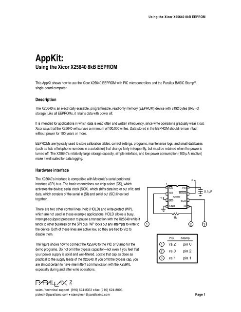
Using the Xicor <strong>X25640</strong> 8kB <strong>EE</strong>PROMAppKit:Using the Xicor <strong>X25640</strong> 8kB <strong>EE</strong>PROMThis AppKit shows how to use the Xicor <strong>X25640</strong> <strong>EE</strong>PROM with PIC microcontrollers and the Parallax BASIC Stamp ®single-board computer.DescriptionThe <strong>X25640</strong> is an electrically erasable, programmable, read-only memory (<strong>EE</strong>PROM) device with 8192 bytes (8kB) ofstorage. Like all <strong>EE</strong>PROMs, it retains data with power off.It is intended for applications in which data is read often and written infrequently, since write operations gradually wear it out.Xicor says that the <strong>X25640</strong> will survive a minimum of 100,000 writes. Data stored in the <strong>EE</strong>PROM should remain intactwithout power for 100 years or more.<strong>EE</strong>PROMs are typically used to store calibration tables, control settings, programs, maintenance logs, and small databases(such as lists of telephone numbers in a autodialer) that change fairly infrequently, but must be retained when the power isturned off. The <strong>X25640</strong>’s relatively large storage capacity, simple interface, and low power consumption (100 µA inactive)make it well suited for data logging.Hardware interfaceThe <strong>X25640</strong>’s interface is compatible with Motorola’s serial peripheralinterface (SPI) bus. The basic connections are chip select (CS), whichactivates the device; serial clock (SCK), which shifts data into or out of it; anddata, which consists of the serial in (SI) and serial out (SO) lines tiedtogether.There are two other control lines, hold (HOLD) and write-protect (WP),which are not used in these example applications. HOLD allows a busy,interrupt-equipped processor to pause a transaction with the <strong>X25640</strong> while ittends to other business on the SPI bus. WP locks out any attempts to write tothe device. Both of these lines are active low, so they are tied to Vcc todisable them.The figure shows how to connect the <strong>X25640</strong> to the PIC or Stamp for thedemo programs. Do not omit the bypass capacitor—not even if you feel thatyour power supply is solid and well-filtered. Locate that cap as close aspractical to the supply leads of the <strong>X25640</strong>. If you omit the bypass cap, youare almost certain to have intermittent communication with the <strong>X25640</strong>,especially during and after write operations.+51CS VccSO HOLD 0.1µF+5 <strong>X25640</strong>WP SCKGND SI1k1 2 3PIC Stamp1 ra.2 pin 02 ra.0 pin 23 ra.1 pin 1sales / technical support (916) 624-8333 • fax (916) 624-8003pictech@parallainc.com • stamptech@parallaxinc.com Page 1
Using the Xicor <strong>X25640</strong> 8kB <strong>EE</strong>PROMSoftware interfaceFrom a software standpoint, using the <strong>X25640</strong> boils down to this:(1) Activate CS by taking it low.(2) Send an instruction (opcode) to the <strong>X25640</strong> telling it what you want to do.(3) If you are reading or writing a memory location, send the address.(4) If you are reading data, shift it into the controller (PIC or Stamp).(5) If you are writing data, shift it out to the <strong>X25640</strong>.(6) Deactivate CS by making it high.The program listings and Xicor data sheet show these processes in detail.Tips for using the <strong>X25640</strong>• When you first apply power to <strong>X25640</strong>, writes are disabled. After completion of a write cycle, the <strong>EE</strong>PROM alsodisables writes. As in the demo programs, you must send the write-enable instruction (WREN) before writing to the<strong>EE</strong>PROM. You can write-protect particular blocks of the <strong>EE</strong>PROM using the write-status-register (WRSR) instruction;see the Xicor data sheet, page 4.• After you have written data to the <strong>X25640</strong>, it begins an internal programming cycle. It takes as much as 10 milliseconds(ms) to complete the write. PIC and BASIC Stamp II users should check the busy flag by reading the status register asshown in the program listings before attempting further reads or writes. The busy bit is least-significant bit (lsb) of thestatus register and reads high when busy. Users of the Stamp I will find that the write cycle is complete in the timebefore the Stamp can read the status register, so it’s generally safe to ignore the busy bit or program a short time delayto ensure that the programming cycle is done.• If you need to write to several sequential addresses of the <strong>X25640</strong>, take advantage of the page-write capability,described on pages 4 and 6 of the Xicor data sheets. You can write up to 32 bytes sequentially, provided that youdon't cross a page boundary (located at 32n-1: 31, 63, 95, 127...). If you write beyond the edge of a 32-byte pageboundary, you will overwrite the lowest addresses of the same page. For example, say you write 5 bytes starting ataddress 29. The bytes would be written to addresses 29, 30, 31, 0, 1. The advantage to a page write is that up to 32bytes may be stored in a single 10-ms programming cycle. A page write starts exactly like the writes demonstrated inthe programs, but instead of raising CS after one data byte, hold CS low and keep feeding additional bytes to the chipusing the Shout subroutine. When you’re finished sending bytes, raise CS.sales / technical support (916) 624-8333 • fax (916) 624-8003pictech@parallainc.com • stamptech@parallaxinc.com Page 2
Using the Xicor <strong>X25640</strong> 8kB <strong>EE</strong>PROMPIC Program Listing; Program: XICOR8K.SRC; Routines to read and write the XICOR <strong>X25640</strong> 8k serial <strong>EE</strong>PROM; via a three-wire serial interface.; Connect the PIC pins below to the like-named pins of the <strong>X25640</strong>.; If you change these connections, be sure to change these equates; the values DataIn and DataOut so that the DATA line is; an input during reads and an output during writes. If the <strong>EE</strong>PROM; shares a port with other I/O, make sure that the values you give; to DataIn and DataOut correctly set the data direction for the; other pins as well. For the purposes of this program, DataIn just; consists of a 1 in the bit position corresponding to the DATA pin; assignment. Since the DATA pin is in position 0 (ra.0), DataIn; is 0001.DATA = ra.0SCK = ra.1CS = ra.2DataIn = 1DataOut = 0; Opcodes for XICOR 25640:WREN = 6 ; Write-enable.WRDI = 4 ; Write-disable.RDSR = 5 ; Read status register.WRSR = 1 ; Write status register (not used here).READ = 3 ; Read the <strong>EE</strong>PROM.WRITE = 2 ; Write to the <strong>EE</strong>PROM.org 8shifts ds 1 ; Shift counter.addrH ds 1addrL ds 1<strong>EE</strong>data ds 1temp ds 1; Device data and reset vectordevice pic16c55,xt_osc,wdt_off,protect_offreset startorg 0;This program write-enables the <strong>EE</strong>PROM, writes a byte to one of its; memory locations, waits for the write-in-progress bit of the status; register to reset (indicating that the write is complete), then; reads back the previously written data.sales / technical support (916) 624-8333 • fax (916) 624-8003pictech@parallainc.com • stamptech@parallaxinc.com Page 3
Using the Xicor <strong>X25640</strong> 8kB <strong>EE</strong>PROMPIC Program Listing (cont)start mov ra,#4 ; Initialize ra with CS high (<strong>EE</strong>PROM off).mov !ra,#DataOut ; Set data direction to output.mov !rc,#0 ; Make all of rc output for LEDs.clr rccall Write_enable ; Send write-enable opcode to <strong>EE</strong>PROM.mov addrH,#01fh ; Now set up the <strong>EE</strong>PROM address (0-1FFFh).mov addrL,#0ffhmov <strong>EE</strong>data,#99 ; And data to be written to that address.call Write_byte ; Write the data.call Write_disable:loop call Read_Status ; Get status byte and check its 0th bit.jb <strong>EE</strong>data.0,:loop ; The bit will stay high until write is done.; For the sake of this demo, we move the address into the high and low; address bytes (addrH and addrL), but it's not really necessary. They; weren't altered by Write_byte, so we could really skip this step.:read mov addrH,#01fh ; Rewrite the <strong>EE</strong>PROM address.mov addrL,#0ffhcall Read_byte ; Read the byte.mov rc,<strong>EE</strong>data ; Show the recovered data on LEDsjmp $ ; Stop the program here.; Subroutine shifts the eight bits of the byte pointed to; by the fsr out to the SI pin of the <strong>X25640</strong>.Shout mov shifts,#8:loop clrb SCKrlindirectmovb DATA,csetb SCKdjnz shifts,:looprlindirectret; Subroutine shifts one byte of serial data from the XDATA; pin into the byte pointed to by the fsr. The nop may be required; at PIC clock speeds above 4 MHz, especially if the resistor; from SI to SO is larger than 1k. If the <strong>EE</strong>PROM incorrectly; sets the msbs of bytes stored at odd-numbered addresses, you; need a smaller resistor, the nop, or both. (The explanation for; the odd symptom is that the lsb of the address output shows up; in the msb of the data input. XICOR says that the <strong>X25640</strong> may; require up to 400 ns from a falling clock edge to valid data; at SO. Combine this with whatever time SO needs to go from; hi-Z to output, and you've got this telltale error.)sales / technical support (916) 624-8333 • fax (916) 624-8003pictech@parallainc.com • stamptech@parallaxinc.com Page 4
Using the Xicor <strong>X25640</strong> 8kB <strong>EE</strong>PROMPIC Program Listing (cont)Shinmov !ra,#DataInmov shifts,#8:loop clrb SCKnopmovb c,DATArlindirectsetb SCKdjnz shifts,:loopmov !ra,#DataOutret; Nop may be required at high speeds.; Returns the contents of the <strong>EE</strong>PROM's status register in; <strong>EE</strong>data. Uses <strong>EE</strong>data to shift out the op code.Read_statusmovmovclrbcallcallsetbretfsr,#<strong>EE</strong>dataindirect,#RDSRCSShoutShinCS; Reads the <strong>EE</strong>PROM data at the address specified by addrH and addrL; and writes it to the location <strong>EE</strong>data.Read_bytemovmovclrbcallmovcallmovcallmovcallsetbretfsr,#tempindirect,#READCSShoutfsr,#addrHShoutfsr,#addrLShoutfsr,#<strong>EE</strong>dataShinCS; Turns off the <strong>EE</strong>PROM's write protection. Must be called; after power up in order to write to the <strong>EE</strong>PROM.sales / technical support (916) 624-8333 • fax (916) 624-8003pictech@parallainc.com • stamptech@parallaxinc.com Page 5
Using the Xicor <strong>X25640</strong> 8kB <strong>EE</strong>PROMPIC Program Listing (cont)Write_enablemovmovclrbcallsetbretfsr,#<strong>EE</strong>dataindirect,#WRENCSShoutCS; Turns on the <strong>EE</strong>PROM's write protection feature to prevent accidental; overwriting of memory in the event that a program goes out of control.Write_disablemovclrbcallsetbretindirect,#WRDICSShoutCS; Writes the byte in <strong>EE</strong>data to the <strong>EE</strong>PROM address specified by addrH; and addrL. The contents of <strong>EE</strong>data, addrH and addrL, are not; changed, although the bits may be a little dizzy from being rapdily; rotated by the trip through Shout.Write_bytemovmovclrbcallmovcallmovcallmovcallsetbretfsr,#tempindirect,#WRITECSShoutfsr,#addrHShoutfsr,#addrLShoutfsr,#<strong>EE</strong>dataShoutCSsales / technical support (916) 624-8333 • fax (916) 624-8003pictech@parallainc.com • stamptech@parallaxinc.com Page 6
Using the Xicor <strong>X25640</strong> 8kB <strong>EE</strong>PROMBASIC Stamp I (BS1-IC) and BASIC Stamp Ver. D Program Listing' Program: XICOR8K.BS1' This program demonstrates subroutines for storing data in a' XICOR <strong>X25640</strong> serial <strong>EE</strong>PROM using the original BASIC Stamp (BS1).Symbol CS = 0 ' Chip-select line to pin 0.Symbol CLK = 1 ' Clock line to pin 1.Symbol DATA = pin2 ' Destination of Shout; input to ShinSymbol DATA_N = 2 ' Pin # of DATA for "input" & "output"Symbol Read<strong>EE</strong> = 3 ' <strong>EE</strong>PROM opcode for read.Symbol WREN = 6 ' <strong>EE</strong>PROM opcode to enable writes.Symbol WRDI = 4 ' <strong>EE</strong>PROM opcode to disable writes.Symbol RDSR = 5 ' <strong>EE</strong>PROM opcode to read the status register.Symbol Write<strong>EE</strong> = 2 ' <strong>EE</strong>PROM opcode for write.Symbol i = b6 ' Counter for shift loopsSymbol <strong>EE</strong>data = b4 ' Data byte to/from <strong>EE</strong>PROMSymbol <strong>EE</strong>addr = w1 ' 16-bit <strong>EE</strong>PROM address.Symbol Shreg = b1 ' Shift register used by Shin/Shout.' Beginning of demonstration program. We're just going to write-enable' the <strong>EE</strong>PROM, write a value to one of its addresses, then retrieve' that value.Demo:output DATA_Nhigh CS' Output to <strong>EE</strong>PROM data lines.' Deactivate <strong>EE</strong>PROM.' This chunk of code sends the write-enable opcode to the <strong>EE</strong>PROM.' To disable writes, use this same code, but substitute WRDI for WREN.let Shreg = WREN ' Write-enable opcode.low CS' Activate the <strong>EE</strong>PROM.gosub Shout' Send the opcode.high CS' Deactivate the <strong>EE</strong>PROM.' ===================================================================' Now write some data to the <strong>EE</strong>PROM. The legal range of addresses' is 0 to 8191.let <strong>EE</strong>data = 195 ' Sample data.let <strong>EE</strong>addr = 800 ' Set an address.gosub <strong>EE</strong>write ' Write the data.pause 10' Wait for write cycle to finish.gosub <strong>EE</strong>read' Read back the data.debug <strong>EE</strong>data' Show us.here:goto here' Endless loop to terminate program.sales / technical support (916) 624-8333 • fax (916) 624-8003pictech@parallainc.com • stamptech@parallaxinc.com Page 7
Using the Xicor <strong>X25640</strong> 8kB <strong>EE</strong>PROMBASIC Stamp I and Ver. D Program Listing (cont.)' ==================================================================' The subroutines for reading and writing the <strong>EE</strong>PROM.' ==================================================================' Shift data into Shreg.Shin:input DATA_Nlet Shreg=0for i = 1 to 8low CLKlet Shreg=Shreg*2let bit8=DATAhigh CLKnext ioutput DATA_Nreturn' Shift data out of Shreg.Shout:for i = 1 to 8low CLKlet DATA=bit15let Shreg=Shreg*2high CLKnext ireturn' Write <strong>EE</strong>data to <strong>EE</strong>addr.<strong>EE</strong>write:let Shreg = Write<strong>EE</strong>gosub Send_addrlet Shreg = <strong>EE</strong>datagosub Shouthigh CSreturn' Change the data line to input.' Clear data byte.' Prepare to get 8 bits.' Data valid on falling edge.' Shift Shreg to the left.' Move data to lsb of variable.' End of clock pulse.' Get another bit.' Restore data line to output.' Shift out 8 bits.' Clear clock bit.' Get bit 7 of Shreg.' Shift register to the left.' Data valid on rising edge of clock.' Send another bit.' Set up the write opcode.' Send it and the address.' Now send the data.' Deactivate the <strong>EE</strong>PROM.' Read data at <strong>EE</strong>addr and put it into <strong>EE</strong>data.<strong>EE</strong>read:let Shreg = Read<strong>EE</strong> ' Set up the read opcode.gosub Send_addr ' Send it and the address.gosub Shin' Now get the data.let <strong>EE</strong>data = Shreg ' Transfer from Shreg to <strong>EE</strong>data.high CS' Deactivate the <strong>EE</strong>PROM.returnsales / technical support (916) 624-8333 • fax (916) 624-8003pictech@parallainc.com • stamptech@parallaxinc.com Page 8
Using the Xicor <strong>X25640</strong> 8kB <strong>EE</strong>PROMBASIC Stamp I and Ver. D Program Listing (cont.)' Send the opcode and address for write or read.Send_addr:low CS' Activate the <strong>EE</strong>PROM.gosub Shout' Send opcode in Shreg.let Shreg = b3 ' Send upper byte of address.gosub Shoutlet Shreg = b2 ' Send lower byte of address.gosub Shoutreturnsales / technical support (916) 624-8333 • fax (916) 624-8003pictech@parallainc.com • stamptech@parallaxinc.com Page 9
Using the Xicor <strong>X25640</strong> 8kB <strong>EE</strong>PROMBASIC Stamp II (BS2-IC) Program Listing' Program: XICOR8K.BS2' This program demonstrates subroutines for storing data in a' XICOR <strong>X25640</strong> serial <strong>EE</strong>PROM using the BASIC Stamp II (BS2).CS con 0 ' Chip-select line to pin 0.CLK con 1 ' Clock line to pin 1.DATA_N con 2 ' Pin # (2) of DATA line.Read<strong>EE</strong> con 3 ' <strong>EE</strong>PROM opcode for read.WREN con 6 ' <strong>EE</strong>PROM opcode to enable writes.WRDI con 4 ' <strong>EE</strong>PROM opcode to disable writes.RDSR con 5 ' <strong>EE</strong>PROM opcode to read status register.Write<strong>EE</strong> con 2 ' <strong>EE</strong>PROM opcode for write.<strong>EE</strong>addr var word ' <strong>EE</strong>PROM address for reads or writes.<strong>EE</strong>data var byte ' Data written/read to/from <strong>EE</strong>PROM.<strong>EE</strong>stats var byte ' Copy of the <strong>EE</strong>PROM status register.<strong>EE</strong>busy var <strong>EE</strong>stats.bit0 ' <strong>EE</strong>PROM busy bit.' Demonstration program. We're just going to write-enable' the <strong>EE</strong>PROM, write a value to one of its addresses, then retrieve' that value.Demo:high CS' Deactivate <strong>EE</strong>PROM.pause 100' Wait for settling.<strong>EE</strong>data = 113 ' Write the value 113 to address 8191.<strong>EE</strong>addr = 8191gosub <strong>EE</strong>nable' Enable the <strong>EE</strong>PROM for writes.gosub <strong>EE</strong>write' Write the data.is_busy:' Stay in a loop until <strong>EE</strong>PROM finishes write.gosub Read_stats ' Read status register.if <strong>EE</strong>busy = 1 then is_busy ' Wait until busy bit says 'done.'gosub <strong>EE</strong>read' Now read back the data and..debug ? <strong>EE</strong>data ' ..display it on the PC screen.STOP' End program.' ==================================================================' The subroutines for reading and writing the <strong>EE</strong>PROM.' ==================================================================' Write-enable the <strong>EE</strong>PROM.<strong>EE</strong>nable:low CSshiftout DATA_N,CLK,msbfirst,[WREN]high CS' Deactivate the <strong>EE</strong>PROM.return' Activate the <strong>EE</strong>PROM.' Send the enable opcode.' Return to program.sales / technical support (916) 624-8333 • fax (916) 624-8003pictech@parallainc.com • stamptech@parallaxinc.com Page 10
Using the Xicor <strong>X25640</strong> 8kB <strong>EE</strong>PROMBASIC Stamp II Program Listing (cont)' Write-protect (disable) the <strong>EE</strong>PROM.<strong>EE</strong>disable:low CSshiftout DATA_N,CLK,msbfirst,[WRDI]high CS' Deactivate the <strong>EE</strong>PROM.return' Write data to the <strong>EE</strong>PROM. Use the address in <strong>EE</strong>addr' and data in <strong>EE</strong>data.<strong>EE</strong>write:low CS' Activate the <strong>EE</strong>PROM.shiftout DATA_N,CLK,msbfirst,[Write<strong>EE</strong>]gosub Send_addr ' Send the address.shiftout DATA_N,CLK,msbfirst,[<strong>EE</strong>data]high CS' Deactivate the <strong>EE</strong>PROM.return' Read data from the <strong>EE</strong>PROM. Use the address in <strong>EE</strong>addr;' put data into <strong>EE</strong>data.<strong>EE</strong>read:low CS' Activate the <strong>EE</strong>PROM.shiftout DATA_N,CLK,msbfirst,[Read<strong>EE</strong>]gosub Send_addr ' Send the address.shiftin DATA_N,CLK,msbpre,[<strong>EE</strong>data]high CS' Deactivate the <strong>EE</strong>PROM.return' Send the address for a read or write.Send_addr:shiftout DATA_N,CLK,msbfirst,[<strong>EE</strong>addr\16]return' Read the <strong>EE</strong>PROM status register.Read_stats:low CSshiftout DATA_N,CLK,msbfirst,[RDSR]shiftin DATA_N,CLK,msbpre,[<strong>EE</strong>stats]high CS' Deactivate the <strong>EE</strong>PROM.return' Activate the <strong>EE</strong>PROM.' Send the disable opcode.' Send write opcode.' Send the data.' Return to program.' Send the read opcode.' Send the data.' Return to program.' Shift the address out.' Return to program.' Activate the <strong>EE</strong>PROM.' Send read-status opcode.' Get the status register.' Return to program.sales / technical support (916) 624-8333 • fax (916) 624-8003pictech@parallainc.com • stamptech@parallaxinc.com Page 11
Using the Xicor <strong>X25640</strong> 8kB <strong>EE</strong>PROMsales / technical support (916) 624-8333 • fax (916) 624-8003pictech@parallainc.com • stamptech@parallaxinc.com Page 12
Using the Xicor <strong>X25640</strong> 8kB <strong>EE</strong>PROMsales / technical support (916) 624-8333 • fax (916) 624-8003pictech@parallainc.com • stamptech@parallaxinc.com Page 13
Using the Xicor <strong>X25640</strong> 8kB <strong>EE</strong>PROMsales / technical support (916) 624-8333 • fax (916) 624-8003pictech@parallainc.com • stamptech@parallaxinc.com Page 14
Using the Xicor <strong>X25640</strong> 8kB <strong>EE</strong>PROMsales / technical support (916) 624-8333 • fax (916) 624-8003pictech@parallainc.com • stamptech@parallaxinc.com Page 15
Using the Xicor <strong>X25640</strong> 8kB <strong>EE</strong>PROMsales / technical support (916) 624-8333 • fax (916) 624-8003pictech@parallainc.com • stamptech@parallaxinc.com Page 17
Using the Xicor <strong>X25640</strong> 8kB <strong>EE</strong>PROMsales / technical support (916) 624-8333 • fax (916) 624-8003pictech@parallainc.com • stamptech@parallaxinc.com Page 18
Using the Xicor <strong>X25640</strong> 8kB <strong>EE</strong>PROMsales / technical support (916) 624-8333 • fax (916) 624-8003pictech@parallainc.com • stamptech@parallaxinc.com Page 19
Using the Xicor <strong>X25640</strong> 8kB <strong>EE</strong>PROMsales / technical support (916) 624-8333 • fax (916) 624-8003pictech@parallainc.com • stamptech@parallaxinc.com Page 20