Design strategies for an FPGA-based 256-channel digital down ...
Design strategies for an FPGA-based 256-channel digital down ...
Design strategies for an FPGA-based 256-channel digital down ...

You also want an ePaper? Increase the reach of your titles
YUMPU automatically turns print PDFs into web optimized ePapers that Google loves.
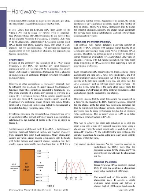
HardwareReconfigurable <strong>FPGA</strong>sCommercial ASICs feature as m<strong>an</strong>y as four ch<strong>an</strong>nels per chip,like the popular Texas Instruments/Graychip GC4016.IP core DDCs, like the LogiCore DDC from Xilinx <strong>for</strong> itsVirtex-II Pro, c<strong>an</strong> be scaled <strong>for</strong> various levels of Spurious-Free Dynamic R<strong>an</strong>ge (SFDR) per<strong>for</strong>m<strong>an</strong>ce to use more or lessof the available resources. For example, a complex DDC with84 dB SFDR consumes approximately 1,700 slices. In a mid-sized<strong>FPGA</strong> device with 24,000 available slices, only about 14 DDCch<strong>an</strong>nels c<strong>an</strong> be accommodated. For applications requiringseveral dozen or even hundreds of ch<strong>an</strong>nels, this approach c<strong>an</strong>become impractical.Ch<strong>an</strong>nelizersBecause of the extremely fine resolution of its NCO tuningfrequency, a true DDC c<strong>an</strong> tr<strong>an</strong>slate <strong>an</strong>y input frequencycomponent <strong>down</strong> to 0 Hz, often with 32-bit accuracy. This abilitymakes DDCs ideal <strong>for</strong> applications that require precise ch<strong>an</strong>gesin tuning such as in continuous Doppler correction <strong>for</strong> satellitetracking systems.However, in other applications, a ch<strong>an</strong>nelizer approach maybe sufficient. This is a b<strong>an</strong>k of equally spaced, fixed frequencyb<strong>an</strong>d pass filters whose outputs are tr<strong>an</strong>slated to baseb<strong>an</strong>d (0 Hz).One crude example of a ch<strong>an</strong>nelizer familiar to everyone is asimple FFT. It converts a block of N time samples equally spacedin time into block of N frequency samples equally spaced infrequency. For a continuous stream of input time sample blocks,samples at a given point in successive output blocks represent atr<strong>an</strong>slated, b<strong>an</strong>d pass frequency signal or bin.By selecting the output of a particular bin, a ch<strong>an</strong>nelizer c<strong>an</strong> serveas a primitive DDC, but with extremely coarse tuning resolutiondetermined by the number of points in the FFT, as shown inFigure 2.Another serious limitation of the FFT as a DDC is the frequencyresponse (pass b<strong>an</strong>d flatness) of the bin, <strong>an</strong>d rejection of energyfrom adjacent bins (stop b<strong>an</strong>d rejection). Other ch<strong>an</strong>nelizerdesigns use various <strong>digital</strong> filtering techniques to split the b<strong>an</strong>dswith better flatness <strong>an</strong>d adjacent ch<strong>an</strong>nel rejection, but theyusually require signific<strong>an</strong>tly more hardware th<strong>an</strong> <strong>an</strong> FFT <strong>for</strong> aBIN 1BIN 2BIN 3comparable number of bins. Regardless of its design, the tuningresolution of <strong>an</strong>y ch<strong>an</strong>nelizer is simply equal to the number ofbins or ch<strong>an</strong>nel filters. As a result, ch<strong>an</strong>nelizers may be useful<strong>for</strong> spectrum <strong>an</strong>alyzers, sc<strong>an</strong>ners, <strong>an</strong>d energy survey equipmentbut they are rarely used as substitutes <strong>for</strong> DDCs in software radiocommunication systems.Rethinking the multich<strong>an</strong>nel DDCThe software radio market generates a growing number ofrequests <strong>for</strong> DDC solutions with densities higher th<strong>an</strong> the 16 or32 ch<strong>an</strong>nels provided per board using ASICs or st<strong>an</strong>dard <strong>FPGA</strong>designs. There<strong>for</strong>e, we embarked upon a mission to develop asignal processing architecture <strong>for</strong> a narrowb<strong>an</strong>d DDC with 64ch<strong>an</strong>nels or more, with full tuning resolution, but with muchmore efficient use of <strong>FPGA</strong> resources th<strong>an</strong> deploying a farm ofconventional DDC cores.Each conventional DDC requires its own local oscillator (phaseaccumulator <strong>an</strong>d sine table), mixer (two multipliers), <strong>an</strong>d FIRfilter (multipliers <strong>an</strong>d accumulators). All of this hardware mustoperate at the full input sample clock rate, <strong>an</strong>d clock rates <strong>for</strong>A/Ds commonly used in software radios r<strong>an</strong>ge between 100<strong>an</strong>d 200 MHz. Since this is the same clock r<strong>an</strong>ge rating <strong>for</strong>commercial DDC IP cores, all of the hardware resources used <strong>for</strong>each ch<strong>an</strong>nel must be dedicated to that ch<strong>an</strong>nel.However, imagine that the input data sample rate is reduced bya factor N. By operating the DDC hardware resources required<strong>for</strong> one ch<strong>an</strong>nel at the full clock rate, those same resources c<strong>an</strong>then be multiplexed (time shared) across N ch<strong>an</strong>nels. Of course,provisions must be made <strong>for</strong> buffering the data <strong>for</strong> all ch<strong>an</strong>nelswhile multiplexing. This is usually done in RAM or in delaymemory, a common feature in <strong>FPGA</strong>s.One way to achieve this input rate reduction is to split theinput signal into a b<strong>an</strong>k of N adjacent frequency b<strong>an</strong>ds using ach<strong>an</strong>nelizer. Then, the output sample rate <strong>for</strong> each b<strong>an</strong>d c<strong>an</strong> bereduced by a factor of N. The output from the b<strong>an</strong>d containing thesignal of interest c<strong>an</strong> be selected as the input to <strong>an</strong>y given DDC tofine tune within that b<strong>an</strong>d.The tradeoff question becomes: Are the resources freed up bymultiplexing the DDCs more th<strong>an</strong> theresources required <strong>for</strong> the ch<strong>an</strong>nelizer? The<strong>an</strong>swer lies in how efficient the ch<strong>an</strong>nelizerc<strong>an</strong> be.INPUTSample Rate= FsFFT1024POINTSSample Rate= Fs/1024AmplitudeRealizing the designFigure 3 shows <strong>an</strong> <strong>FPGA</strong>-<strong>based</strong> <strong>256</strong>-ch<strong>an</strong>nelDDC IP core that combines a ch<strong>an</strong>nelizerstage with a multiplexed DDC stage.BIN 1022BIN 1023BIN 1024Figure 2BINnBINn+1BINn+2BINn+3FreqThe crucial part of this design is thech<strong>an</strong>nelizer stage. It accepts a singlewideb<strong>an</strong>d input stream <strong>an</strong>d delivers ach<strong>an</strong>nel b<strong>an</strong>k of 1,024 output b<strong>an</strong>ds equallyReprinted from Military Embedded Systems Summer 2006 Copyright 2006