Military Embedded Systems - Fall 2005 - Volume 1 Number 2
Military Embedded Systems - Fall 2005 - Volume 1 Number 2
Military Embedded Systems - Fall 2005 - Volume 1 Number 2

Create successful ePaper yourself
Turn your PDF publications into a flip-book with our unique Google optimized e-Paper software.
Open<strong>Systems</strong> Publishing<br />
BONUS SHOW DISTRIBUTION:<br />
G S P x , S D R F O RU M<br />
<strong>Military</strong><br />
The COTS Technology Authority<br />
EMBEDDED SYSTEMS<br />
Mil Comms=<br />
SDR + FPGAs + DSP<br />
SOFTWARE<br />
SCA’s evolution links<br />
to other specs<br />
HARDWARE<br />
Altera logic<br />
secures mil systems<br />
APPLICATIONS<br />
Low-power<br />
flash storage<br />
PRODUCT GUIDE<br />
SBCs for signal<br />
processing<br />
PICTURED<br />
GE Fanuc<br />
<strong>Embedded</strong><br />
<strong>Systems</strong><br />
Talon 8400
RSC# @www.mil-embedded.com/rsc
RSC# @www.mil-embedded.com/rsc
V O L U M E 1 N U M B E R 2<br />
O C T O B E R 2 0 0 5<br />
w w w . m i l - e m b e d d e d . c o m<br />
<strong>Military</strong><br />
V O L U M E 1<br />
N U M B E R 1<br />
EMBEDDED SYSTEMS<br />
R E S O U R C E G U I D E 2 0 0 5<br />
DEPARTMENTS<br />
Industry Analysis<br />
8 What has happened to product warranties?<br />
By Jerry Gipper<br />
10 Beep, configure, fire<br />
By Don Dingee<br />
12 Trends in military computing<br />
By Joe Pavlat<br />
In the System<br />
16 FPGAs gearing up to dominate DSP applications<br />
By Duncan Young, SBS Technologies<br />
24 Editor’s Choice Products<br />
Crosshairs Editorial<br />
62 We need SDR now<br />
By Chris A. Ciufo<br />
56 New Products<br />
By Sharon Schnakenburg<br />
Product Selection Guide<br />
50 Single board computers for DSP and reconfigurable computing<br />
EVENTS<br />
SDR Forum<br />
Nov. 14-18 • Garden Grove, CA<br />
www.sdrforum.org<br />
<strong>Embedded</strong> Connect<br />
Nov. 17 • Santa Clara, CA<br />
www.esconline.com<br />
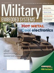
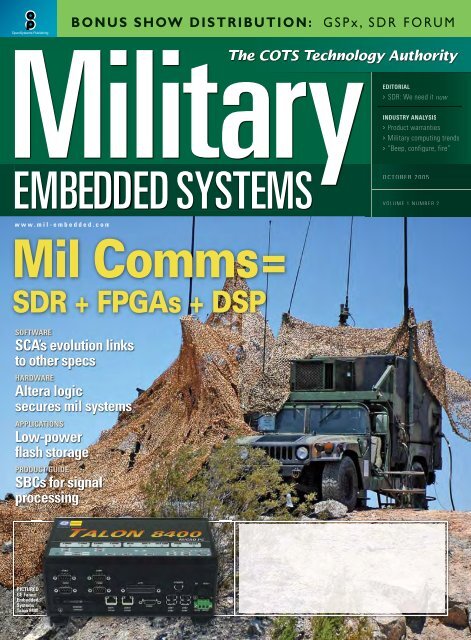
COVER<br />
A Humvee providing communication sits atop<br />
a lonely hill half covered in desert pattern cami<br />
netting. (Photo courtesy of U.S. Marines by<br />
Lance Cpl. Jem J. Hamilton).<br />
PRODUCT<br />
Using internal PC/104-Plus modules, the Talon<br />
8400 by GE Fanuc <strong>Embedded</strong> <strong>Systems</strong> is a selfcontained<br />
PC designed for rugged applications<br />
from -20 °C to +50 °C.<br />
Published by:<br />
©<strong>2005</strong> <strong>Military</strong> <strong>Embedded</strong> <strong>Systems</strong><br />
/ October <strong>2005</strong> <strong>Military</strong> EMBEDDED SYSTEMS<br />
Open<strong>Systems</strong><br />
FEATURES<br />
HARDWARE:<br />
20 Why convert to a SAASM-based GPS?<br />
By Ron Holm, Symmetricom<br />
25 Enabling military design security with high-performance<br />
FPGAs<br />
By Joel Seely & Jie Feng, Altera<br />
SOFTWARE: Software Defined Radio<br />
28 Software communication architecture: Evolution and status<br />
update<br />
By Jeff Smith, Ph.D., David Murotake, Ph.D.,<br />
and Antonio Martin, SCA Technica<br />
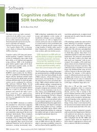
34 Cognitive radios: The future of SDR technology<br />
By Bruce Fette, Ph.D., General Dynamics C4 <strong>Systems</strong><br />
38 Mapping waveforms to systems: What would a wideband<br />
networking waveform system require?<br />
By Kevin Maier, Spectrum Signal Processing<br />
APPLICATION: Performance enhancements<br />
42 FPGA memory controllers improve DSP performance<br />
By Richard M. Matthews, Micro Memory<br />
46 Tapping into solid-state storage benefits for low-power<br />
and small form factor applications<br />
By Gary Drossel, Silicon <strong>Systems</strong><br />
E-LETTER<br />
www.mil-embedded.com/eletter<br />
Net-centric computing: Architecting a distributed data-management<br />
infrastructure<br />
By Bert Farabaugh, RTI<br />
Floss helps you take control of your bytes<br />
By Robert Dewar, AdaCore<br />
Please visit us online for the complete list of articles<br />
WEB RESOURCES<br />
Subscribe to the magazine or E-letter:<br />
www.opensystems-publishing.com/subscriptions
RSC# @www.mil-embedded.com/rsc
Open<strong>Systems</strong> Publishing<br />
Advertising/Business office:<br />
30233 Jefferson Avenue<br />
St. Clair Shores, MI 48082<br />
Tel: 586-415-6500 n Fax: 586-415-4882<br />
BUSINESS OFFICE:<br />
Vice President Marketing & Sales<br />
Patrick Hopper<br />
phopper@opensystems-publishing.com<br />
Business Manager<br />
Karen Layman<br />
ADVERTISING GROUP:<br />
Vice President Marketing & Sales<br />
Patrick Hopper<br />
phopper@opensystems-publishing.com<br />
Senior Account Manager<br />
Dennis Doyle<br />
ddoyle@opensystems-publishing.com<br />
Account Manager<br />
Tom Varcie<br />
tvarcie@opensystems-publishing.com<br />
Print and Online Marketing Specialist<br />
Christine Long<br />
clong@opensystems-publishing.com<br />
Advertising/Marketing Coordinator<br />
Andrea Stabile<br />
astabile@opensystems-publishing.com<br />
European Bureau Chief<br />
Stefan Baginski<br />
sbaginski@opensystems-publishing.com<br />
Account Manager<br />
Doug Cordier<br />
dcordier@opensystems-publishing.com<br />
COMMUNICATIONS GROUP:<br />
Patrick Hopper<br />
phopper@opensystems-publishing.com<br />
Christine Long<br />
clong@opensystems-publishing.com<br />
EMBEDDED GROUP:<br />
Dennis Doyle<br />
ddoyle@opensystems-publishing.com<br />
Doug Cordier<br />
dcordier@opensystems-publishing.com<br />
MILITARY GROUP:<br />
Tom Varcie<br />
tvarcie@opensystems-publishing.com<br />
Andrea Stabile<br />
astabile@opensystems-publishing.com<br />
INTERNATIONAL SALES:<br />
Stefan Baginski<br />
sbaginski@opensystems-publishing.com<br />
<strong>Military</strong><br />
EMBEDDED SYSTEMS<br />
A n O p e n S y s t e m s P u b l i c a t i o n<br />
<strong>Military</strong> and Aerospace Group<br />
n DSP&FPGA Product Resource Guide<br />
n DSP-FPGA.com<br />
n DSP-FPGA.com E-letter<br />
n <strong>Military</strong> <strong>Embedded</strong> <strong>Systems</strong><br />
n <strong>Military</strong> <strong>Embedded</strong> <strong>Systems</strong> E-letter<br />
n PC/104 <strong>Embedded</strong> Solutions<br />
n PC/104 <strong>Embedded</strong> Solutions E-letter<br />
n PC/104 & Small Form Factor Catalog<br />
n VMEbus <strong>Systems</strong><br />
n VMEbus <strong>Systems</strong> E-letter<br />
Group Editorial Director<br />
Managing Editor<br />
Senior Editor (columns)<br />
Assistant Editor<br />
European Representative<br />
Art Director<br />
Senior Web Developer<br />
Graphic Specialist<br />
Chris A. Ciufo<br />
cciufo@opensystems-publishing.com<br />
Bonnie Crutcher<br />
bicrutcher@opensystems-publishing.com<br />
Terri Thorson<br />
tthorson@opensystems-publishing.com<br />
Sharon Schnakenburg<br />
sschnakenburg@opensystems-publishing.com<br />
Hermann Strass<br />
hstrass@opensystems-publishing.com<br />
Steph Sweet<br />
Konrad Witte<br />
David Diomede<br />
Circulation/Office Manager Phyllis Thompson<br />
subscriptions@opensystems-publishing.com<br />
Open<strong>Systems</strong><br />
Publishing Publishing<br />
Editorial/Production office:<br />
16872 E. Ave of the Fountains, Ste 203, Fountain Hills, AZ 85268<br />
Tel: 480-967-5581 n Fax: 480-837-6466<br />
Website: www.opensystems-publishing.com<br />
Publishers<br />
Vice President Editorial<br />
Communications Group<br />
Editorial Director<br />
Assistant Managing Editor<br />
Senior Editor (columns)<br />
Technology Editor<br />
European Representative<br />
John Black, Michael Hopper, Wayne Kristoff<br />
Rosemary Kristoff<br />
Joe Pavlat<br />
Anne Fisher<br />
Terri Thorson<br />
Curt Schwaderer<br />
Hermann Strass<br />
<strong>Embedded</strong> and Test & Analysis Group<br />
Editorial Director<br />
Editorial Director<br />
Associate Editor<br />
Senior Editor (articles)<br />
Technical Editor<br />
Special Projects Editor<br />
European Representative<br />
Jerry Gipper<br />
Don Dingee<br />
Jennifer Hesse<br />
Terri Thorson<br />
Chad Lumsden<br />
Bob Stasonis<br />
Hermann Strass<br />
Canada return address: WDS, Station A, PO Box 54, Windsor, ON N9A 615<br />
<strong>Military</strong> <strong>Embedded</strong> <strong>Systems</strong> is published six times a year by Open<strong>Systems</strong><br />
Publishing LLC., 30233 Jefferson Ave., St. Clair Shores, MI 48082. Subscriptions<br />
are free, upon request in writing, to persons dealing with or considering<br />
<strong>Military</strong> <strong>Embedded</strong> <strong>Systems</strong>.<br />
For others inside the US and Canada, subscriptions are $34/year. For 1st class<br />
delivery outside the US and Canada, subscriptions are $60/year (advance<br />
payment in US funds required).<br />
POSTMASTER: Send address changes to <strong>Military</strong> <strong>Embedded</strong> <strong>Systems</strong><br />
16872 E. Ave of the Fountains, Ste 203, Fountain Hills, AZ 85268<br />
For reprints and PDFs call the sales office: 586-415-6500<br />
/ October <strong>2005</strong><br />
<strong>Military</strong> EMBEDDED SYSTEMS
RSC# @www.mil-embedded.com/rsc
Industry Analysis<br />
What has happened to<br />
product warranties?<br />
By Jerry Gipper<br />
Most embedded electronic<br />
hardware components come<br />
with a standard product<br />
warranty. If a board fails,<br />
you contact the supplier, arrange a repair<br />
or exchange, ship it to the repair center,<br />
and await the repaired or replaced product.<br />
This is a rather routine process amongst<br />
all suppliers worldwide. In the case of<br />
most VME, CompactPCI, and embedded<br />
motherboards, today’s warranties<br />
range from one to three years in duration.<br />
There used to be a time when warranties<br />
from many suppliers were five years<br />
or in some cases, “lifetime” (Figure 1).<br />
What ever happened to those warranties?<br />
Why are they not as common? In the early<br />
1990s there was a lot of noise in the industry<br />
about long or lifetime warranties. Press<br />
releases were distributed touting the warranty<br />
terms, and warranties were highlighted<br />
in advertisements. Suppliers were very<br />
proud of their product reliability and were<br />
willing to stand behind their products.<br />
Years<br />
5<br />
4<br />
3<br />
2<br />
1<br />
0<br />
A quick check today of the same product<br />
types shows typical warranty periods<br />
of only two years, with a few as long as<br />
three years. Certainly these are shorter<br />
than “lifetime.” Has something happened<br />
to the reliability? Has the cost of quality<br />
risen too high to absorb in competitive<br />
pricing strategies?<br />
This change in warranty periods started<br />
quietly happening as companies were<br />
recovering from the dot-com bust in 2001.<br />
No embedded technology suppliers publicly<br />
“announced” their shorter warranty<br />
periods. In fact, the reduced warranty<br />
periods did not hit home until a problem<br />
occurred and a product needed repair. Did<br />
suppliers reduce prices to reflect the shortened<br />
warranty periods? I would venture to<br />
guess prices were not reduced since suppliers<br />
were already under extreme margin<br />
pressures during those times.<br />
Some possible explanations exist as to<br />
why warranties greater than two years are<br />
no longer typical. Any one or more of the<br />
Warranty Length<br />
What<br />
happens<br />
here?<br />
1980 1985 1990 1995 2000 <strong>2005</strong> 2010<br />
Figure 1<br />
following are key factors in determining<br />
warranty terms and pricing:<br />
n<br />
n<br />
n<br />
Increased cost of quality: By<br />
definition, the Cost Of Poor<br />
Quality (COPQ) consists of costs<br />
generated as a result of producing<br />
defective material. Additional cost<br />
includes all the labor cost, rework<br />
cost, disposition cost, utilities cost,<br />
manufacturing cost, and material<br />
cost that has been added to the unit<br />
up to the point of rejection. It also<br />
includes the cost of lost opportunity<br />
due to the loss of resources used in<br />
rectifying the defect. The cost of lost<br />
opportunity means lower revenue<br />
and profit, potential loss of market<br />
share, and a lower service level to<br />
customers. All areas of cost in COPQ<br />
have increased in past years.<br />
Speed of technology: In general,<br />
the technologies used in embedded<br />
computing systems are still relatively<br />
new. New technologies evolve rapidly,<br />
and rapidly evolving technologies<br />
have a shorter product life cycle.<br />
Getting the quality to an acceptable<br />
level can be a challenge at best with<br />
many of the newer technologies. Do<br />
designers and manufacturers always<br />
fully understand the quality issues of<br />
one technology before moving on to<br />
the next?<br />
Pursuit of quality: With products’<br />
shorter life cycles, perhaps the race<br />
to have the best and most optimized<br />
set of features at a competitive price<br />
has pushed quality into the backseat.<br />
Products today have manufacturing<br />
lives less than three years in duration.<br />
In most cases, the quality is not<br />
fully optimized in that short of a life<br />
cycle. Suppliers move on to the next<br />
generation before they really get the<br />
kinks out of the existing products.<br />
Sometimes designers may take<br />
shortcuts or use unproven design<br />
elements to meet time-to-market<br />
pressures. With the low quantities<br />
and high mix of the embedded space,<br />
/ October <strong>2005</strong><br />
<strong>Military</strong> EMBEDDED SYSTEMS
Industry Analysis<br />
n<br />
it is hard to spend too much time on<br />
quality for any single product line. Is<br />
enough simulation and accelerated<br />
life testing being done?<br />
Lost the recipe: Perhaps<br />
manufacturers simply “lost the<br />
recipe” when changing manufacturing<br />
locations as mergers occurred or<br />
manufacturing was transferred<br />
offshore to large, high-volume<br />
contract manufacturers to save costs.<br />
The embedded industry tends to<br />
build products in small lots with<br />
a high mix of different types and<br />
product versions. The manufacturing<br />
efficiency is never very high in these<br />
situations. Moving to a high-volume,<br />
low mix manufacturing facility only<br />
frustrates the manufacturing process<br />
in these cases. As a result, quality<br />
suffers immensely. Lower quality<br />
levels mean higher warranty costs<br />
and loss of ability to absorb these<br />
costs in competitive prices. Most<br />
manufacturing operations are great at<br />
n<br />
building high-quality products, and<br />
vendors fully understand the nuances<br />
of quality manufacturing; however,<br />
it takes high repetitions of the same<br />
steps and processes to really reach the<br />
best quality levels.<br />
Service as a profit center: Maybe<br />
the answer is as simple as using<br />
warranties as a way to increase the<br />
revenue stream. Most embedded<br />
board suppliers have extensive repair<br />
and service centers. Removing the<br />
cost of the warranty from the<br />
product cost and making it a<br />
separate price line item is a<br />
way for the service centers to<br />
improve their revenue streams<br />
and justify their existence. It<br />
does make it easier to develop<br />
custom and innovative service<br />
programs that better fit the<br />
customer’s needs.<br />
What is going to happen to warranty<br />
terms in the future? It is<br />
possible that the Restriction of<br />
the use of certain Hazardous<br />
Substances (RoHS) or the Waste<br />
from Electric and Electronic<br />
Equipment (WEEE) initiatives<br />
being driven out of Europe and<br />
Asia will force further tightening<br />
of warranty terms. Suppliers may<br />
use this as the compelling event<br />
to tighten the warranty programs<br />
even more. Two-year warranties<br />
could easily become one-year<br />
warranties in the next one to<br />
two years.<br />
However, all is not lost as many<br />
suppliers in the embedded<br />
industry offer various extended<br />
warranty programs that can be<br />
customized to meet the specific<br />
needs of consumers. These programs<br />
have options for warranty<br />
periods and coverage that can<br />
help manage costs for the lifetime<br />
of a program. Extended warranties<br />
are insurance against a future<br />
failure. Be sure to check out all<br />
your options when planning lifetime<br />
costs for your products.<br />
For more information, you may<br />
contact Jerry directly at<br />
jgipper@opensystemspublishing.com.<br />
RSC# @www.mil-embedded.com/rsc<br />
<strong>Military</strong> EMBEDDED SYSTEMS<br />
October <strong>2005</strong> /
Industry Analysis<br />
Beep, configure, fire<br />
By Don Dingee<br />
<strong>Military</strong> planners are now talking in terms of<br />
plug-and-fight capability. This is a spin on the old<br />
personal computing term plug-and-play – catchy,<br />
but outdated. As a marketing person at heart, I can’t<br />
help but suggest an updated term that better describes what we<br />
see taking place and what elements are going into this capability.<br />
Most of us have seen some version of the movie scene where the<br />
condemned prisoners are paraded out in blindfolds, lined before<br />
a wall, and a firing squad is issued the familiar cliché “Ready,<br />
aim, fire!”<br />
Today, with electronics driving most combat systems, a more<br />
appropriate term for the plug-and-fight process would be “Beep,<br />
configure, fire!”<br />
and adapt computing hardware to better fit immediate requirements.<br />
Linux-based open system architectures allow clusters (just<br />
another term for systems-of-systems) to add distributed nodes easily,<br />
enabling distributed processing and sensor fusion capability<br />
quickly and reliably.<br />
It’s the intersection of processor, network fabric, and operating<br />
system in a reconfigurable form that becomes interesting. One<br />
example of this is the CoSine from Micro Memory. Built on the<br />
Xilinx Virtex-4 FPGA family with VxWorks running on two<br />
PowerPC 405 cores, it includes connectivity for serial RapidIO<br />
or PCI Express, a corner-turning Direct Memory Access (DMA)<br />
engine to aid in data movement, and a user-programmable area<br />
for signal processing algorithms. (Refer to the Micro Memory<br />
article on page 42 in this issue.)<br />
Beep – Join the network<br />
For today’s warfighter, there is a wealth of<br />
information and intelligence available in<br />
real time as close as the nearest network.<br />
Sensor and command data fused into the<br />
network from a variety of modes and locations<br />
enable a tactical system to quickly<br />
access reliable information on the mission<br />
plan, threat situation, and the configuration<br />
of neighboring defense systems.<br />
Recently, I visited a friend in the San Francisco Bay area, and<br />
he was showing me his new Bluetooth-enabled phone and headset.<br />
He commented that he could not help but notice that when<br />
he wears the headset while driving, especially on the freeways,<br />
he hears frequent beeps as the headset attempts to connect with<br />
devices in neighboring vehicles. It’s almost too easy to connect<br />
to a network now.<br />
Short-range wireless networks provide a continuous network<br />
tone and have made it easy to connect quickly to a wide variety of<br />
devices. Technologies such as Bluetooth, Wi-Fi, Ultrawideband,<br />
Wireless USB, and the longer-range WiMax may soon be enabled<br />
with a security layer, enabling their use in defense applications.<br />
For now, defense networks using Software Defined Radio (SDR)<br />
technologies fit the bill.<br />
Planners talk of systems fitting into a netted, distributed force.<br />
Whether wired or wireless, today’s defense systems-of-systems<br />
are built around network-centric designs and rely on being able<br />
to join the network quickly.<br />
“Today, with electronics driving most<br />
combat systems, a more appropriate<br />
term for the plug-and-fight process<br />
would be ‘Beep, configure, fire!’”<br />
Additionally, advances are being<br />
made in Linux on FPGA platforms.<br />
The University of Queensland in Australia<br />
recently secured a contract for NASA’s<br />
Reconfigurable Scalable Computing (RSC)<br />
project, building from a starting point in<br />
which a version of uClinux is adapted to<br />
the Xilinx MicroBlaze soft-core processor.<br />
The ultimate goal will be to remotely<br />
(as in ground-to-space) partially reprogram<br />
FPGAs on the fly.<br />
We may see that general-purpose processors ultimately give way<br />
to reconfigurable processors in defense applications, both for<br />
functional and life-cycle reasons. Teamed with the University of<br />
Southern California and using IBM Cu-08 90 nm process technology,<br />
Raytheon’s Morphable Networked Micro-Architecture<br />
(MONARCH) project targets April 2008 for a device that can<br />
alternate instantaneously between front-end (streaming) and<br />
back-end (threaded) processing.<br />
According to Jack Kelble, president of Raytheon Space and<br />
Airborne <strong>Systems</strong>, “In the past, a bank of processor boards<br />
accepted information and another bank processed it.” He added,<br />
“Now a tiny but highly sophisticated device a fraction of the size<br />
will perform both functions with unprecedented speed, power, and<br />
capacity to store and process a vast amount of data.” MONARCH<br />
is expected to perform in a single chip or SoC role, possibly significantly<br />
reducing the number and types of processors required<br />
for computing systems. In the latter application, it will be<br />
able to process incoming and outgoing data while analyzing it.<br />
Configure – Compute for effect<br />
Reconfigurable computing has advanced an incredibly long way<br />
in recent years. Advances in System-on-Chip (SoC) technology<br />
combining processing with FPGAs allow designers to optimize<br />
Fire – With open weapons<br />
Using technologies such as these, networked, reconfigurable<br />
weapons systems are beginning to emerge as the norm. Initiatives<br />
including the Modular Open <strong>Systems</strong> Approach (MOSA) spon-<br />
10 / October <strong>2005</strong> <strong>Military</strong> EMBEDDED SYSTEMS
sored by The Open <strong>Systems</strong> Joint Task Force within the US<br />
Department of Defense continue to set higher expectations.<br />
Openness in new acquisitions is being demanded as seen in<br />
these comments from Lieutenant General Ronald E. Keys<br />
in February <strong>2005</strong>: “We’ve got to get to this thing called the<br />
‘compatible open architecture.’ I’ve got to be able to truly<br />
plug-and-play, and it’s got to plug-and-play better than Microsoft.<br />
It’s actually got to plug, boot up, recognize, and work … So don’t<br />
bring me stuff that’s not compatible because I’m not going to<br />
be happy.”<br />
Large combat systems already architecting around plug-andfight<br />
concepts include the Medium Extended Air Defense System<br />
(MEADS), Future Combat <strong>Systems</strong> (FCS), and the Littoral<br />
Combat Ship (LCS).<br />
MEADS is the US Army’s next-generation replacement for<br />
Nike Hercules, Hawk, and Patriot air-defense missile systems,<br />
designed from the ground up to move with ground forces and<br />
interoperate with other allied forces. It relies heavily on networking<br />
and distributed intelligence to achieve its mission.<br />
A MEADS system has the capability to command a fleet of<br />
distributed missile launchers while simultaneously detecting<br />
and tracking hostile forces and targets. There is a key tactical<br />
advantage to this distributed design: The missile launchers<br />
can be located well away from the ground radar and the<br />
battle management units, reducing the risk of detection of the<br />
launchers. This tactical advantage also opens the possibility to<br />
transfer command and control of the launchers and missiles to<br />
a neighboring battle management unit, while some management<br />
systems are offline for whatever reason.<br />
Industry Analysis<br />
Researchers at the University of Essex are working on a concept<br />
called the gridswarm, where small Unmanned Aerial Vehicles<br />
(UAVs) capable of speeds up to 120 mph fly in formations similar<br />
to the flocking behavior of small birds. In the prototype, these aircraft<br />
are connected by a Bluetooth mesh driven by Linux compute<br />
modules from Gumstix. These tiny modules run Linux 2.6 on 400<br />
MHz Intel Xscale processors with 64 MB DRAM and 4 MB Flash,<br />
along with USB, serial, and optional Bluetooth interfaces. It’s a<br />
great example of small systems fitting into larger systems fitting<br />
into still larger systems with aggregated intelligence.<br />
Rapid developments in wireless networking, reconfigurable<br />
computing, and network-centric weapons systems are going to<br />
spawn new innovations quickly. The results should also reduce<br />
the long-term costs of weapons procurement, enabling easier<br />
upgrades and reducing the impact of obsolescence by allowing<br />
subsystem level replacements.<br />
I’ll be sure to tell my friend the next time I see him that<br />
when he hears a whole bunch of beeps in rapid succession<br />
on his Bluetooth headset, he should duck. It could<br />
be a UAV gridswarm reconfiguring just overhead, and hopefully<br />
they are unarmed and peace loving.<br />
If you happen to see a gridswarm, or other interesting developments<br />
that beep and configure, drop me a line.<br />
For more information, contact Don at ddingee@opensystemspublishing.com.<br />
FCS isn’t a single system but rather a blended system-of-systems<br />
intended to transform the US Army’s fighting capability.<br />
Underlying FCS is a software architecture called Fire Control<br />
– Node Engagement Technology (FC-NET). FC-NET provides<br />
an adaptable, flexible architecture that modularizes the interaction<br />
between the technical weapon system (the intelligence that<br />
controls and guides the weapon) and the tactical information systems.<br />
This enables weapon systems to readily join the command<br />
fabric to get the information they require.<br />
Another plug-and-fight system is LCS. It’s being designed to<br />
work in three primary mission areas for the US Navy, including<br />
mine countermeasures, anti-submarine warfare, and<br />
anti-surface warfare, presumably with anti-air, self-defense<br />
capability in each role. This is being accomplished through<br />
the design of mission packages that fit into the sea frame<br />
and adapt the capability to the desired mission area. Opensystems<br />
architecture and modular, networked subsystems<br />
are again the key to success, and the notion of being able to<br />
reconfigure the system for the role at hand is prominent in the<br />
architecture.<br />
Open doesn’t mean big<br />
Creating new systems-of-systems isn’t necessarily about<br />
using big computers. From the looks of things, it could be just<br />
the opposite, using networks of relatively small processors tied<br />
together wirelessly with very intelligent software and combining<br />
these systems into larger systems.<br />
RSC# 11 @www.mil-embedded.com/rsc<br />
<strong>Military</strong> EMBEDDED SYSTEMS October <strong>2005</strong> / 11
Industry Analysis<br />
Trends in military computing<br />
By Joe Pavlat<br />
A changing landscape<br />
These are good times for designers of<br />
military computer systems, as the range<br />
of choices and the breadth of applications<br />
and requirements is greater than ever<br />
before. Traditionally, military electronics<br />
have been extremely expensive, usually<br />
purpose-designed and uniquely built<br />
for each application. <strong>Systems</strong> often do<br />
not communicate with each other, making<br />
future net centric warfare difficult.<br />
Reuse of hardware and software has been<br />
the exception rather than the norm, and<br />
design cycles historically have been long<br />
and expensive. Industry insiders often talk<br />
about the large “flywheel” in the military<br />
computer business, meaning that development<br />
cycles are long, and revenues<br />
are often years away. The one open standard<br />
embraced for military applications,<br />
the VMEbus, arguably has been widely<br />
accepted not for its blazing performance<br />
but rather because the standard was first<br />
published more than 20 years ago –<br />
a veritable lifetime for the rest of the<br />
computer industry.<br />
The flywheel is still quite large, but it is<br />
rotating a bit more quickly these days.<br />
Open industry standards are becoming<br />
more popular. Former Secretary<br />
of Defense William Perry’s famous COTS<br />
directive was a factor, but the same development<br />
cost and time-to-deployment<br />
pressures that affect the commercial computer<br />
world affect military suppliers. Two<br />
PCI Industrial Computer Manufacturers<br />
Group (PICMG) standards, PICMG 1.0<br />
(PCI-ISA Passive Backplane, 1994) and<br />
PICMG 2.0 (CompactPCI, 1995), were<br />
released 11 and 10 years ago respectively,<br />
and are used for a variety of military<br />
applications worldwide.<br />
A wide range of open<br />
standards<br />
PICMG’s first published specification, the<br />
PCI-ISA Passive Backplane Specification<br />
released in 1994, is being used in a wide<br />
range of applications, including the onboard<br />
fire control computer for the M109<br />
Palladin self-propelled howitzer used<br />
extensively in Operation Iraqi Freedom.<br />
Companies such as BES <strong>Systems</strong> Ltd.<br />
in Israel offer a complete range of ruggedized<br />
airborne, vehicle, and naval<br />
computers compliant to the PICMG 1.1<br />
specification, additionally providing compliance<br />
to military standards including<br />
MIL-STD-810E, which dictates tough<br />
requirements for shock, vibration, humidity,<br />
fungus, salt and dust, and fog.<br />
Figure 1<br />
Released in 1995, the CompactPCI<br />
standard was developed for ruggedized<br />
industrial applications. It offered then<br />
state-of-the-art performance, based on<br />
ubiquitous PCI silicon available from virtually<br />
every microprocessor and peripheral<br />
chip manufacturer. It was based on<br />
the same IEEE 1101.1 mechanical standard<br />
used by VME, and it became very<br />
popular for communications applications<br />
worldwide. Defined for both 3U and 6U<br />
form factors, the 6U size became popular<br />
for the vast majority of communications<br />
applications, which needed every<br />
square inch of real estate for components.<br />
The 3U form factor has historically been<br />
used largely for instrumentation and some<br />
industrial automation applications, but<br />
was not as widely embraced as the larger<br />
6U form factor.<br />
This has been changing over the last few<br />
years in a dramatic fashion. Specially<br />
ruggedized 3U CompactPCI products are<br />
being used for a wide variety of airborne,<br />
vehicle, and even space-based systems.<br />
One example is the AVC-CPCI 3009 system<br />
offered by SBS Technologies, developed<br />
for Unmanned Aerial Vehicle (UAV)<br />
applications (see Figure 1, photo courtesy<br />
of SBS Technologies, Inc.). Its integrated<br />
frame grabber and MPEG-4 image compressor<br />
connect directly to the airframe’s<br />
onboard camera, forwarding data in real<br />
time to war planners on the ground.<br />
<strong>Systems</strong> are also going into space.<br />
Aitech’s S950 3U CompactPCI SBC is<br />
conduction-cooled and offers a PowerPC<br />
750FX CPU (see Figure 2, photo courtesy<br />
of Aitech Defense <strong>Systems</strong>, Inc.).<br />
It is rated to operate in Low Earth<br />
Orbit, Geosynchronous Orbit, and Mars<br />
Terrestrial environments.<br />
The 6U CompactPCI systems are also<br />
being used for military applications.<br />
Performance Technologies, Inc. builds<br />
a sophisticated Mission LAN System<br />
using the PICMG 2.16 CompactPCI<br />
Packet Switched Backplane standard.<br />
Intended to be part of a National<br />
12 / October <strong>2005</strong> <strong>Military</strong> EMBEDDED SYSTEMS
Industry Analysis<br />
Better architectures hit<br />
the ground<br />
One hears a great deal about transforming<br />
the military from the current platformcentric<br />
approach to network-centric operations.<br />
The underlying computer technologies,<br />
including chips and software, are<br />
also undergoing fundamental change, and<br />
it is good news for designers and users of<br />
military computers.<br />
Command Center aboard a heavily modified<br />
Boeing 707 aircraft known as the<br />
TACAMO, the system maintains communication<br />
and control in the event that<br />
other command centers are damaged<br />
or destroyed. It provides networking<br />
and routing within the aircraft, handling<br />
packetized radio, satellite, radar, and<br />
laser transmissions, and ties together<br />
different systems on the plane (see<br />
Figure 3, photo courtesy of Performance<br />
Technologies, Inc.).<br />
Performance Technologies has also<br />
developed a unique hybrid CompactPCI/<br />
Figure 2<br />
VME system for use in the Global Hawk<br />
UAV (see Figure 4, photo courtesy of<br />
Performance Technologies, Inc.). This<br />
computer provides near real-time highresolution<br />
images and intelligence to<br />
field commanders in theater or across<br />
the world. Multicast image streams can<br />
be ordered by a commander in a control<br />
room or a soldier on the ground in the<br />
next valley, providing vital current information<br />
and situational awareness. The<br />
CompactPCI boards are conduction cooled<br />
and compliant with the ANSI/VITA 30.1<br />
specification (2 mm connector practice for<br />
conduction-cooled Eurocard systems).<br />
Most backplane interconnect technologies,<br />
including VME and CompactPCI, are<br />
based on chip-level interconnects that<br />
were intended for planar motherboards.<br />
Hot swap was not an integral part of these<br />
interconnects, and their parallel nature<br />
has meant that any board plugged into the<br />
backplane could cause the entire system<br />
to fail if it failed. Full 2N redundancy was<br />
often the only solution. Focus was placed<br />
on reliability instead of the much more useful<br />
concept of availability because parallel<br />
bus architectures just do not adapt well<br />
to high availability designs, which require<br />
system management and failure domains<br />
of a single board. Also, as core chip<br />
voltages go ever lower, the notion of<br />
distributing chip supply voltages often<br />
means that parallel backplanes are required<br />
to produce hundreds, or even thousands,<br />
of amps of current for large systems.<br />
IP/Radio<br />
Ground Communications<br />
Satellite Uplink/Downlink<br />
Radars<br />
10/100/1000 TX<br />
RS-232/RS422/1553<br />
Connections<br />
Five<br />
<strong>Systems</strong>/Aircraft<br />
Command and Control<br />
Figure 3<br />
<strong>Military</strong> EMBEDDED SYSTEMS October <strong>2005</strong> / 13
Industry Analysis<br />
Extractors<br />
Heat Sink<br />
Heat<br />
Transfer<br />
Slugs<br />
Mezzanine Cover<br />
to write and maintain cumbersome Board<br />
Support Packages (BSPs), which often<br />
need updating every time a chip on the<br />
board changes revision. The Application<br />
Programming Interface (API) approach<br />
moves that responsibility to the chip<br />
supplier and operating system, making<br />
systems easier to upgrade and maintain.<br />
Expensive RTOSs are beginning to give<br />
way to less expensive and increasingly<br />
powerful OSs such as Real-Time Linux<br />
and Carrier-Grade Linux.<br />
Wedge Locks<br />
This is changing for the better. Primarily,<br />
in order to increase data transfer speed,<br />
the microprocessor industry is moving<br />
rapidly towards switched serial interconnect<br />
technology, popularly known as<br />
switch fabrics. This technology reduces<br />
the speed-robbing capacitance typical of<br />
a parallel bus architecture with instantaneous<br />
point-to-point interconnects. Not<br />
only do these interconnects increase data<br />
transmission speed one or two orders of<br />
magnitude, which is important for military<br />
applications such as imaging, they can,<br />
if properly designed, reduce the failure<br />
domain to a single board or Field<br />
Replaceable Unit (FRU). They also dramatically<br />
improve the scalability of military<br />
systems, as the same packetized data<br />
format used over the backplane can be<br />
used between boxes or systems in a large<br />
network. Switched fabric Ethernet-based<br />
backplane standards, first introduced to<br />
Figure 4<br />
the world in 2001 in the PICMG 2.16<br />
Specification, are beginning to be used<br />
for military applications.<br />
Additionally, power distribution concepts<br />
are changing with an emphasis toward<br />
shipping higher voltages across backplanes<br />
in order to reduce the ever-increasing<br />
currents required by Moore’s Law.<br />
(We’ll save cooling problems for another<br />
time.) Localized power conversion is the<br />
norm in standards like AdvancedTCA<br />
and PICMG’s recently ratified advanced<br />
mezzanine card standards.<br />
An entire book could be written about<br />
software development, but as much as<br />
advances in this arena seem to trail hardware<br />
progress, a few things can be said.<br />
Spurred by the wide adoption of the PCI<br />
bus 10 years ago, military board suppliers<br />
are increasingly being freed from the need<br />
Notions are changing<br />
In the commercial communications sector,<br />
the distinction between datacom and telecom<br />
is all but gone as the world’s infrastructure<br />
moves towards packet-based<br />
communications. <strong>Military</strong> infrastructure,<br />
at least in the US, is joining the movement.<br />
Major initiatives, such as the Department<br />
of Defense’s Warfighter Information<br />
Network Tactical (WIN-T) program, are<br />
based on commercial communication<br />
technologies, including secure wireless<br />
networks, Voice over Internet Protocol<br />
(VoIP), PCS cellular services, and ATM<br />
data transport. PDAs, laptops, and tablet<br />
computers are widely used in American<br />
command centers worldwide, and e-mail<br />
is as ubiquitous and important as it is in<br />
the civilian sector. The old notions about<br />
ruggedized military computers being<br />
completely customized boxes milled out<br />
of large bars of aluminum are changing.<br />
And they are changing for the better as<br />
the flywheel spins faster.<br />
For more information, contact Joe at<br />
jpavlat@opensystems-publishing.com.<br />
Crystal P4 875<br />
♦Dual 10/100/1000 network Ethernet<br />
♦Up to 800 MHz FSB supporting 128k<br />
through 2MB L2 Cache<br />
♦PICMG 1.2 with 64 bit/66 MHz support<br />
♦Two SATA, One Ultra ATA/100, Floppy support<br />
For more information, contact<br />
a Program Manager at:<br />
Hiawatha, Iowa USA 52233-1204<br />
1.800.378.1636 1.319.378.1636<br />
www.crystalpc.com<br />
RSC# 1401 @www.mil-embedded.com/rsc RSC# 1402 @www.mil-embedded.com/rsc RSC# 1403 @www.mil-embedded.com/rsc<br />
14 / October <strong>2005</strong> <strong>Military</strong> EMBEDDED SYSTEMS
Acromag introduces affordable FPGA I/O. For ALL your projects.<br />
As an engineer, your projects are unique,<br />
ever-changing, and budget-bound.That's<br />
why our new PMC modules give you an<br />
affordable solution to create custom I/O boards.<br />
But if you thought FPGA computing was only<br />
for top-end applications, think again. Our<br />
PMCs are ideal for protocol conversion,<br />
simulation, in-circuit testing, and much more.<br />
So why settle for generic I/O when you can<br />
design exactly what you need while staying in<br />
budget and reducing your time to market?<br />
• Virtex ® -II FPGA with 500K,<br />
2M or 3M system gates<br />
• 1Mb on-chip RAM,<br />
9Mb on-board SRAM<br />
• Fast PCI with 32-bit,<br />
66MHz dual DMA<br />
Industry Pack FPGA I/O also available<br />
Cost-effective custom I/O<br />
Choose from a variety of I/O configurations:<br />
• Digital I/O: TTL, RS422, or LVDS I/O<br />
• Analog I/O: four 20 or 65MHz A/D and two D/A<br />
Faster time to market<br />
Why waste precious time building a board from<br />
scratch? Our new FPGA modules let you process<br />
your I/O signals any way you want. Quickly.<br />
Flexibility to meet unexpected challenges<br />
Acromag FPGA I/O will help you bring your<br />
projects in on time and under budget. And with<br />
FPGAs, you'll be ready to adapt<br />
to all the inevitable changes.<br />
Thinking about FPGA I/O?<br />
Think flexible. Think affordable.<br />
Think Acromag.<br />
Call or visit our website today –<br />
for VME, CompactPCI, PCI, PMC,<br />
and Industry Pack solutions.<br />
www.acromag.com<br />
800-881-0268 or 248-624-1541<br />
A N A L O G I / O D I G I T A L I / O S E R I A L I / O F P G A C O U N T E R / T I M E R Q U A D R A T U R E<br />
Manufactured in Wixom, Michigan, USA<br />
RSC# 15 @www.mil-embedded.com/rsc All trademarks are the property of their respective companies
In the System<br />
FPGAs gearing up to dominate<br />
DSP applications<br />
By Duncan Young<br />
AltiVec PowerPCs have enjoyed dominance<br />
in high-end military signal processing<br />
applications such as Software-<br />
Defined Radio (SDR) and video/image<br />
compression. But FPGAs, with their<br />
inherent parallelism and reprogrammability,<br />
are fast becoming prevalent and<br />
easily fit on smaller boards such as PCI<br />
Mezzanine Cards (PMCs).<br />
The PowerPC’s AltiVec, 128-bit vector<br />
processor is the undisputed first choice for<br />
DSP where floating-point performance is<br />
the critical decision point. However, the<br />
new breed of FPGA is geared up to wipe<br />
out the AltiVec advantage for the great<br />
variety of the military’s fixed-point DSP<br />
applications. Interestingly, although the<br />
AltiVec has been available for some time<br />
and appears in Freescale Semiconductor’s<br />
recently announced dual-core MPC8641D<br />
embedded processor, there does not<br />
appear to be any interest within the industry<br />
in offering competitive (and hence<br />
better or faster) floating point solutions<br />
for military DSP applications.<br />
FPGAs with their innate parallelism<br />
appear set to oust the traditional multiple-<br />
PowerPC solution from a broad range<br />
of DSP applications. FPGAs offer much<br />
reduced real estate, power consumption,<br />
and cost. Time-to-deployment pressure<br />
from end users is driving some COTS<br />
vendors to offer prepackaged FPGAbased<br />
hardware/software products for<br />
specific application segments.<br />
Let’s talk numbers<br />
The advent of the latest generation of<br />
FPGAs such as the Xilinx Virtex-4 or the<br />
Altera Stratix II — having as many as<br />
100,000 logic cells, 400 DSP Multiply/<br />
Accumulate (MAC) elements and internal<br />
RAM, clocking at over 450 MHz — offers<br />
the potential to migrate and integrate DSP<br />
operations previously only performed by<br />
dedicated processors. The ability to process<br />
multiple data streams in parallel sets<br />
the FPGA solution apart from dedicated<br />
DSP or PowerPC alternatives.<br />
Where ultimate performance is required<br />
on a single channel, the FPGA will always<br />
lose out. The AltiVec can perform a<br />
64 x 64 MAC at single instruction rates<br />
(typically 1.5 GHz), whereas the FPGA<br />
will achieve 450 MHz for an 18 x 18 MAC.<br />
The FPGA’s aggregate throughput from<br />
400 MACs on multiple channels can far<br />
exceed that of a single PowerPC processor<br />
device in most applications. The DSP<br />
system designer can now choose from a<br />
number of design directions:<br />
Front-end processing of<br />
multiple array sensors<br />
Unlike a PowerPC or dedicated DSP<br />
processor, an FPGA offers many MAC<br />
elements to perform operations in parallel<br />
on incoming data streams. Previously<br />
this kind of parallelism required many<br />
PowerPCs to perform repetitive tasks<br />
such as filtering and decimation from<br />
each array of the sensor, with the attendant<br />
data distribution challenges. This<br />
data distribution is simple if all the<br />
PowerPCs are located on, for example,<br />
just a single VMEbus card, but much<br />
more complex if they are spread among<br />
many cards or even racks of cards where<br />
switched fabrics would be required. Using<br />
FPGAs can bring about big reductions at<br />
the critical front end, typically offering<br />
savings equivalent to one FPGA per 10x<br />
PowerPCs. Power, weight, space, complexity,<br />
and cost are conserved.<br />
Complete system-on-chip<br />
fixed-point DSP solutions<br />
The FPGA provides a versatile set of<br />
external interface options such as LVDS,<br />
PCML, LVPECL, and HyperTransport<br />
with which to build multiple types of<br />
sensor interfaces. The DSP and logic elements<br />
can be used for filtering and FFT<br />
operations, plus onboard hard and soft<br />
processor cores and real-time operating<br />
systems are available for logical and system-level<br />
operations. Extensive tool kits<br />
and libraries are available for the development<br />
of FPGA architecture, routing,<br />
and software to suit the final application<br />
requirement.<br />
With the notable exceptions of multiplearray<br />
radar and sonar applications, most<br />
military applications for DSP are relatively<br />
straightforward and can be closely<br />
coupled to the sensor itself. Typical of this<br />
class of application are:<br />
n<br />
n<br />
n<br />
Video and image processing<br />
Communications (SDR)<br />
Weapons system sensors such as<br />
torpedoes, cruise missiles, groundto-air<br />
missiles, air-to-air missiles, or<br />
surveillance UAVs.<br />
Unlike the multiple-array radar and sonar<br />
applications that often use many hundreds<br />
of PowerPC-class processors plus<br />
a switched fabric for interconnection,<br />
these simpler applications listed above<br />
could be implemented by dedicated DSP<br />
devices such as the TigerSHARC, ASICs,<br />
FPGAs, or by a much smaller number of<br />
PowerPC processors.<br />
SDR example<br />
A potential application for a single FPGA<br />
device could be to form the basis of a<br />
typical rugged, man-portable SDR with<br />
multiple secure voice and data channels.<br />
Soft FPGA cores are available for<br />
filtering, and IFFT/FFT modulation and<br />
demodulation using the FPGA’s DSP<br />
elements, plus encryption and decryption<br />
— thus providing a number of communication<br />
channels in just one FPGA<br />
device. To offer complete, system-level<br />
functionality, this configuration needs to<br />
be augmented with external interfaces to<br />
the RF components and the user, plus a<br />
general-purpose processor for operation<br />
of the user interface and regular diagnostics/prognostics<br />
of the completed system.<br />
Required user interfaces are:<br />
n<br />
n<br />
n<br />
n<br />
Serial RS-232/422 channels<br />
Ethernet<br />
USB<br />
Discrete I/O<br />
An ideal packaging solution for an FPGA<br />
front-end is the PMC module. Most<br />
generic SBCs from established military<br />
16 / October <strong>2005</strong> <strong>Military</strong> EMBEDDED SYSTEMS
In the System<br />
in areas such as SDR and video compression-based<br />
surveillance. Bundled COTS<br />
products reduce time-to-deployment to<br />
satisfy new expectations.<br />
The TS-MPEG-4 bundled product from<br />
SBS Technologies shown in Figure 1<br />
illustrates this product packaging strategy.<br />
It is based on a standard air- or conduction-cooled<br />
PMC module with an<br />
Altera Stratix EP1S30 FPGA, 128 MB of<br />
SDRAM, and a PCI interface to the host<br />
SBC. This PMC can be used in its basic<br />
form in many different applications with<br />
the customer developing code to suit.<br />
The external interfaces can be tailored<br />
by means of a unique micro-mezzanine<br />
mounted on the PMC module itself.<br />
In the module’s bundled form, the deliverable<br />
product includes all the code<br />
Figure 1<br />
required for operation out of the box, plus<br />
physical interfaces to two RS-170 video<br />
COTS vendors support the PMC concept<br />
of I/O, as indeed do many PowerPCbased<br />
DSP cards. The PMC module is<br />
independent of the SBC’s processor type<br />
using the FPGA manufacturer’s toolkits.<br />
Some COTS vendors have taken the idea<br />
further and developed prepackaged applications<br />
for their FPGA. PMC modules<br />
sources and one RS-170 video output.<br />
Instead of using DSPs or general-purpose<br />
processors such as AltiVec-equipped<br />
PowerPCs, the supplied FPGA code compresses<br />
or bus architecture (for example VMEbus 1 the two incoming video channels<br />
that 97917.3p4c.COTS_MES include standard hardware 4/6/05 interfaces 3:16 PM Page<br />
or CompactPCI), making it a versatile<br />
platform for many different applications.<br />
In this example, if the FPGA were<br />
implemented on a PMC-fomat module,<br />
it could then be mounted on a COTS<br />
3U CompactPCI host SBC with either<br />
a Pentium or PowerPC processor. This<br />
combination of SBC and PMC would<br />
form the digital portion of the radio and<br />
would only occupy a single 0.8" slot<br />
width, 6.3" deep and 4" high.<br />
and application-ready code can be used using MPEG-4, offering 15 to 20 percent<br />
Time-to-deployment of new<br />
FPGA designs<br />
Time-to-deployment of new technology<br />
has become a critical factor in the military<br />
procurement process. Whereas projects<br />
would once take many years to reach<br />
combat status, with what was by then<br />
obsolete technology, timescales have<br />
shrunk. Introducing new capabilities such<br />
as security and surveillance now demands<br />
not just the latest technology but all the<br />
tools and application support required for<br />
their immediate use.<br />
Though SOC FPGAs promise the benefits<br />
of technology leadership, there is considerable<br />
development effort required to<br />
reach deployment when undertaking new<br />
application designs. This requirement<br />
is so even if it is based on a typical offthe-shelf<br />
solution such as a PMC module<br />
Switch Mode Power Magnetics<br />
PREMIER MAGNETICS is your source for MIL-STD-1553 databus interface transformers<br />
for avionics, fly-by-wire and guidance systems. And we’re your source for switch mode power<br />
supply components–high-frequency transformers, inductors and filter components–complete<br />
with fully-tested reference designs.<br />
Smallest Industry Package Sizes<br />
Competitive Prices<br />
Prompt Delivery<br />
Free Samples<br />
Reference Circuits<br />
P r e m i e r M a g n e t i c s<br />
20381 Barents Sea Circle<br />
Lake Forest, CA 92630<br />
949-452-0511 fax: 949-452-0512<br />
w w w . p r e m i e r m a g . c o m / m e s<br />
RSC# 17 @www.mil-embedded.com/rsc<br />
<strong>Military</strong> EMBEDDED SYSTEMS October <strong>2005</strong> / 17
In the System<br />
better compression ratios than the widely<br />
used MPEG-2 standard. The card then<br />
streams compressed data over the PCI bus<br />
to the host SBC. On the host, the MPEG-<br />
4 stream is encapsulated and passed to a<br />
network connection using UDP. Remote<br />
display clients supplied with the bundle<br />
can then decompress and display the<br />
decoded video streams. It should be noted<br />
that this is an FPGA-based system, reaping<br />
all the benefits of FPGAs that we’ve<br />
been describing.<br />
Surveillance UAV example<br />
Battlefield surveillance UAVs such as the<br />
Altair Predator B variant (Figure 2) are<br />
good examples of where packaged PMCbased<br />
FPGAs like the TS-MPEG-4 could<br />
be used for video capture and compression.<br />
This class of UAV usually flies at<br />
low to medium altitude over a battlefield<br />
or other area of particular interest and<br />
carries a number of video and, possibly,<br />
high-resolution single-shot cameras for a<br />
more detailed view of individual objects.<br />
The UAV will be controlled from a ground<br />
station that receives images from various<br />
cameras and displays them for analysis<br />
by the ground crew. The images may<br />
then also be relayed further up the command<br />
chain to build a complete tactical<br />
picture of the battlefield. The downlink<br />
from the UAV to the ground does not have<br />
the bandwidth to transmit all the video<br />
streams directly from the cameras in real<br />
time, driving the need for compression.<br />
The mission computer for such a UAV<br />
is likely to be implemented using COTS<br />
VMEbus or CompactPCI modules.<br />
Because of the limited space, weight,<br />
and power budgets available in a UAV,<br />
3U CompactPCI would again be an ideal<br />
format choice for the mission computer.<br />
FPGA-based PMC modules for video<br />
compression could be mounted on a host<br />
SBC or could occupy 3U slots using carrier<br />
cards. Video streams direct from<br />
the cameras in RS-170 format would be<br />
converted to MPEG-4 by the FPGAs,<br />
then encapsulated and downlinked by the<br />
mission computer for any of the groundbased<br />
operations required.<br />
The FPGA with its unique and flexible<br />
architecture looks set to replace many of<br />
today’s dedicated DSP solutions where<br />
its parallelism and aggregate throughput<br />
make possible big reductions in real estate<br />
and cost. Equally, the cost of time-todeployment<br />
is becoming a critical factor<br />
for both the government and system integrator,<br />
and FPGA-based solutions often<br />
provide benefits as well. The availability<br />
of bundled, application-oriented COTS<br />
solutions, even though they may require<br />
minor customization for a particular enduse,<br />
promise to bring new FPGA-based<br />
DSP systems online faster and at lower<br />
cost.<br />
Duncan Young has worked in the<br />
defense industry for almost 40 years.<br />
Duncan was part of the management<br />
buyout team that formed Radstone<br />
Technology, and he initiated product<br />
development of conduction-cooled<br />
VMEbus modules. He has also served on<br />
a number of standardization committees.<br />
Duncan is now an independent<br />
consultant and writes this column on<br />
behalf of SBS Technologies.<br />
For more information, contact:<br />
SBS Technologies<br />
2400 Louisiana Blvd. NE, Ste. 5-600<br />
Albuquerque, NM 87110<br />
Tel: 505-875-0600<br />
Website: www.sbs.com<br />
Figure 2<br />
18 / October <strong>2005</strong> <strong>Military</strong> EMBEDDED SYSTEMS
When failure is not an option.<br />
0 921<br />
mph<br />
mph<br />
Vibration issues?<br />
We have the answer.<br />
At 921 mph every part of the F-22 is put to<br />
the ultimate vibration test.<br />
Every electrical connection has to work perfectly...<br />
the pilot is betting his life on it.<br />
All Hypertronics products are built upon the legendary<br />
Hypertac ® Contact which outperforms other interconnect options.<br />
• Immunity to shock and vibration.<br />
• Up to 100,000 mating cycles.<br />
• Nearly half the resistance of conventional contact designs.<br />
• Extremely low insertion and extraction forces.<br />
Ruggedized<br />
VME64x<br />
Connectors<br />
Where reliablity<br />
and speed of<br />
data transfer<br />
are a necessity<br />
I N T E R C O N N E C T S O L U T I O N S<br />
ISO 9001, 13485, & 14001 certified Hudson, MA 1-888-HYPERTAC www.hypertronics.com<br />
Visit Hypertronics at MEECC - May 16th & 17th - Long Beach, CA - www.meecc.com<br />
RSC# 19 @www.mil-embedded.com/rsc
Hardware<br />
Why convert to a SAASM-based<br />
Global Positioning System?<br />
By Ron Holm<br />
In 1998, the Joint Chiefs of Staff<br />
selected the Selective Availability<br />
Anti-Spoofing Module (SAASM) as the<br />
security architecture to bring the Global<br />
Positioning System (GPS) to the next<br />
level, and issued the following<br />
mandate: As of October 1, 2006, all<br />
newly fielded Department of Defense<br />
(DoD) GPS systems will use SAASMcompliant<br />
Precise Positioning System<br />
(PPS) devices. Procurement of non-<br />
SAASM GPS user-equipment will be<br />
disallowed unless waived.<br />
Despite a government mandate requiring<br />
all newly fielded DoD GPS systems to<br />
use SAASM-compliant PPS devices by<br />
October 2006, many military groups and<br />
other federal agencies continue to purchase<br />
receivers without SAASM compliance.<br />
<strong>Military</strong> users purchasing a GPS<br />
receiver without SAASM, or anyone who<br />
waits until the October 2006 deadline, is<br />
taking a security risk. Standard GPS service<br />
could be denied at any time via warfare<br />
tactics such as jamming or spoofing,<br />
and if this occurs, GPS receivers without<br />
SAASM will find it difficult to correct<br />
the situation quickly because the process<br />
to acquire SAASM-compliant receivers<br />
requires significant time for authorization<br />
and processing.<br />
We are going to explain what SAASM is all<br />
about, why it’s important to GPS receiver<br />
end-users, and why those who deploy non-<br />
SAASM receivers are putting their organization<br />
at risk right now – even though<br />
the deadline is less than a year away.<br />
Sense of urgency<br />
The need for improving GPS security<br />
came to the forefront even more this<br />
past December in an announcement by<br />
President George W. Bush in which he<br />
issued the Space-Based Positioning,<br />
Navigation, and Timing (PNT) policy. The<br />
PNT policy authorizes the improvement<br />
of the United States’ capabilities to deny<br />
hostile use of any space-based positioning,<br />
navigation, and timing services without<br />
unduly disrupting civil and commercial<br />
access. In the policy, the President specifically<br />
directed the Secretary of Defense to<br />
develop and maintain navigation warfare<br />
capabilities required to effectively utilize<br />
GPS services in the event of jamming or<br />
other interference by adversaries.<br />
This announcement underscores the fact<br />
that the federal government is increasing<br />
the level of urgency to safeguard<br />
GPS. The pressure for government<br />
agencies and military units to convert<br />
to SAASM-compliant GPS receivers<br />
is bound to also increase dramatically.<br />
Along with the selection of SAASM by<br />
the Joint Chiefs, the writing on the wall is<br />
clear: All defense agencies should begin<br />
converting to SAASM GPS receivers.<br />
SAASM explained<br />
To understand the risks and why it’s<br />
important to deploy SAASM-compliant<br />
GPS receivers as soon as possible, a brief<br />
recap of GPS and SAASM will help.<br />
GPS has come to play a significant role<br />
in our everyday tasks during the past<br />
decade. GPS makes it possible to pinpoint<br />
the precise location of any person<br />
or place, anywhere in the world. It helps<br />
with everyday things such as how to drive<br />
our vehicles from Point A to Point B<br />
via onboard navigation systems.<br />
Spoofing and encrypted coding<br />
GPS spoofing involves the intentional sending of a fake GPS signal by a simulated<br />
satellite mimicking a legitimate GPS satellite. Spoofing produces a false reading in<br />
GPS SPS devices and, if properly executed, can introduce position and timing errors,<br />
disrupting navigation and communication systems.<br />
The low-power GPS satellite transmitters deliver extremely low-strength signals<br />
(equivalent to 0.0000000000000001 watt) to Earth-based GPS receivers that are vulnerable<br />
to jamming and spoofing. Jammers are inexpensive, unintelligent electronic<br />
devices that merely produce a higher-power blocking signal at the GPS frequency.<br />
Jamming is disruptive but usually detected by the GPS receiver as it stops tracking<br />
satellites. Spoofing requires more sophisticated, expensive equipment. Spoofing poses<br />
a particular security risk as it is often undetected by a GPS SPS device.<br />
The key to preventing spoofing is to deploy<br />
a GPS receiver that can acquire encrypted<br />
GPS signals referred to as P(Y) coded signals,<br />
which are more robust and jam resistant. GPS<br />
satellites broadcast two signals: a civilian,<br />
unencrypted signal (referred to as C/A) that<br />
all GPS receivers can access, and the military<br />
encrypted coded signal P(Y). GPS devices<br />
in compliance with SAASM can receive and<br />
decrypt the P(Y) code (when keyed), which<br />
authenticates that the signal originated from<br />
the GPS satellites. The code frequency ranges<br />
are shown centered about L1 in Figure 1.<br />
P(Y)-Code<br />
C/A-Code<br />
L1<br />
1575.42 MHz<br />
20 / October <strong>2005</strong> <strong>Military</strong> EMBEDDED SYSTEMS
Hardware<br />
GPS has also become critically important<br />
to the military to identify the whereabouts<br />
of friends and foes, and it plays a crucial<br />
role in the success of military operations<br />
by providing precise time and frequency<br />
to communication systems. This allows<br />
military units to synchronize movements<br />
and ensure they communicate over secure<br />
frequency bandwidths that change on<br />
an irregular basis to avoid detection by<br />
the enemy.<br />
for everyone, including the military. SPS<br />
utilizes a simpler, unprotected C/A code<br />
that is openly available to commercial,<br />
civil, and military users.<br />
The GPS signals are transmitted on two<br />
L-band frequencies: L1 (1575.42 MHz)<br />
and L2 (1227.60 MHz). The SPS service<br />
is provided on L1 and the PPS service on<br />
both L1 and L2.<br />
Manufacturers of SAASM GPS receiver<br />
modules and the products that they are<br />
integrated into, referred to as PPS Host<br />
Application Equipment (HAE), must<br />
work closely with the Key Data Processor<br />
Loading and Installation Facility (KLIF)<br />
under strict guidelines. After manufacturing<br />
the SAASM unit, the GPS receiver<br />
manufacturer ships the SAASM hardware<br />
to the KLIF for the loading of the Key<br />
Data Processor (KDP) crypto software.<br />
Since GPS relies on low-powered frequency<br />
waves traveling from satellites to<br />
GPS receivers on the ground, the technology<br />
also lends itself to intentional jamming<br />
by enemies as well as unintentional<br />
or intentional jamming by allies. For<br />
example, the Civil Coarse Acquisition<br />
(C/A) code signal may be intentionally<br />
jammed by the US and other allies<br />
to allow only SAASM and legacy P(Y)<br />
receivers to access GPS. GPS is also susceptible<br />
to enemy spoofing – the deliberate<br />
attempt to mimic a legitimate signal<br />
and introduce erroneous position and time<br />
information.<br />
Manufacture<br />
Receiver with<br />
SAASM Module<br />
KLIF<br />
KDP Software<br />
Loaded<br />
Manufacture<br />
GPS Basic Operation<br />
Software Loaded<br />
Register<br />
with<br />
KLIF<br />
Shipped<br />
to<br />
Customer<br />
To combat this situation, the US government<br />
launched a program in the 1990s<br />
referred to as SAASM. SAASM deploys<br />
anti-spoofing measures using cryptography<br />
to protect authorized users from false<br />
satellite signals generated by an enemy.<br />
To understand the reasons for SAASM,<br />
it helps to have an understanding of the<br />
components of the GPS system used by<br />
people, organizations, and governments<br />
throughout the world.<br />
GPS mini-history<br />
Through a satellite navigation system,<br />
GPS provides positioning and clock<br />
time to GPS receivers on the earth.<br />
Conceptualized in 1973, the first GPS satellite<br />
was launched in 1978, and in 1995<br />
the system became fully operational.<br />
Today the system consists of 28 satellites<br />
orbiting 12,500 miles above the Earth.<br />
GPS was originally intended as a military<br />
force enhancement system but now<br />
serves dual purposes: GPS has evolved<br />
to improve not only military security but<br />
also the accuracy of the position, velocity,<br />
and time of any object on earth – securely<br />
to military users and freely to civil users.<br />
GPS does this by offering two positioning<br />
services: Precise Positioning Service<br />
(PPS) for authorized military users only<br />
and Standard Positioning Service (SPS)<br />
The DoD relies upon GPS as the primary<br />
source for position, navigation, time,<br />
and time synchronization. Therefore, the<br />
GPS network was also built to allow for<br />
the deployment of security measures.<br />
Selective Availability (SA) is a security<br />
technique that involves the introduction<br />
of intentional errors into the GPS signal,<br />
which denies full system accuracy to SPS<br />
users. On 2 May 2000, however, the effects<br />
of SA were set to zero and it appears<br />
unlikely SA will ever be set higher. But<br />
the potential still exists, and this would<br />
degrade the accuracy of GPS for SPS users.<br />
Anti-Spoofing (A-S) utilizes cryptography<br />
and special keys to protect a GPS PPS<br />
receiver from receiving false satellite<br />
signals generated by an adversary.<br />
The SAASM manufacturing and<br />
integration process<br />
The detailed regulations that the US government<br />
has applied to the SAASM manufacturing<br />
process clearly demonstrate<br />
how serious GPS security has become<br />
and the need for immediate conversion to<br />
SAASM-compliant receivers.<br />
Figure 1<br />
After return of the SAASM device to the<br />
manufacturer, production test is completed<br />
and the unit is ready for sale to JPO<br />
approved customers.<br />
Figure 1 shows the SAASM GPS receiver<br />
manufacturing process and integration<br />
into PPS HAE.<br />
SAASM receivers support two key types<br />
to decrypt anti-spoofing and remove<br />
selective availability:<br />
Physical-form red keys are classified, and<br />
distribution is closely protected since red<br />
keys are unencrypted.<br />
Newer, black keys, on the other hand,<br />
are encrypted and unclassified. They<br />
can be distributed and loaded electronically,<br />
although paper tape distribution<br />
is still common. The decryption of the<br />
key only takes place within the secure<br />
SAASM module. Black keys may be<br />
renewable in the future via Over-The-<br />
Air-Rekeying (OTAR). Black keys<br />
make sense because they solve key distribution<br />
problems and are useless to<br />
<strong>Military</strong> EMBEDDED SYSTEMS October <strong>2005</strong> / 21
Hardware<br />
the enemy because they are encrypted.<br />
The DoD recognizes the security,<br />
delivery, and cost savings associated with<br />
black keys and wants users to transition<br />
from red to black keys as soon as possible<br />
(Figure 2).<br />
To ensure security of the classified technology<br />
within a SAASM receiver and to<br />
preclude unauthorized procurement, the<br />
Navstar GPS Joint Program Office (JPO)<br />
at the Space and Missile <strong>Systems</strong> Center<br />
at Los Angeles AFB ensures compliance<br />
to DoD security requirements. All developers,<br />
integrators, and users of SAASM<br />
GPS must be JPO authorized.<br />
SAASM developers and manufacturers<br />
must also meet several strict requirements,<br />
including securing a Communications<br />
Security (COMSEC) account, a KLIF<br />
account, and undergoing a complete JPO<br />
design-review process. Developers and<br />
manufacturers also have to prove they<br />
are free of foreign ownership, control,<br />
and influence and that they have a facility<br />
security clearance issued by the Defense<br />
Security Service (DSS).<br />
<strong>Military</strong> end-users must receive authorization<br />
from the JPO to procure SAASMbased<br />
devices. When proper authorization<br />
occurs, the JPO issues a formal letter so<br />
that authorized manufacturers of SAASM<br />
GPS receivers will know authorization<br />
has formally been granted.<br />
Figure 2<br />
Benefits of SAASM GPS<br />
receivers<br />
By purchasing a SAASM receiver now,<br />
authorized users comply with the DoD GPS<br />
security architecture and possess the most<br />
secure GPS technology to enhance their<br />
ability to use precise positioning, velocity,<br />
and time in all environments. SAASMbased<br />
GPS receivers have the capability<br />
to directly acquire the encrypted, military<br />
GPS code and no longer have to depend<br />
on the often-jammed civil GPS code.<br />
The need for deploying a SAASM receiver<br />
could become critical at any moment<br />
since access to the Standard GPS service<br />
(SPS) could be denied via warfare tactics<br />
focused on local and regional denial<br />
(jamming) of the civil code within an area<br />
of conflict. In addition to losing access<br />
to the signal, upgrading GPS SPS based<br />
systems to SAASM is nontrivial since the<br />
process to acquire product and distribute<br />
the keys that can decrypt coded signals<br />
requires significant time for authorization<br />
and processing.<br />
Without a doubt, those military and<br />
government agencies that wait until the<br />
SAASM deadline approaches in October<br />
2006 are taking a security risk. If an enemy<br />
source attempts to jam or spoof the GPS<br />
signal, users of non-SAASM receivers<br />
could lose all of their GPS capabilities.<br />
Ron Holm is a product<br />
marketing manager<br />
for Symmetricom and<br />
manages the GPS<br />
Time and Frequency<br />
Instrumentation product<br />
line. Ron has been<br />
involved in the time<br />
and frequency industry since 1990 and<br />
has held previous positions in engineering<br />
and engineering management. Ron<br />
holds a bachelor’s degree in electronic<br />
engineering from the University of<br />
Minnesota.<br />
To learn more, contact Ron at:<br />
Symmetricom<br />
2300 Orchard Parkway<br />
San Jose, CA, 95131<br />
Tel: 408-964-7619<br />
E-mail: ttm_sales@symmetricom.com<br />
Website: www.symmetricom.com<br />
The views expressed in this article are those of the<br />
author and do not necessarily reflect the official policy<br />
or position of the Navstar GPS Joint Program Office,<br />
the Air Force, the Department of Defense, or the U.S.<br />
government.<br />
This article has been modified from the original<br />
October <strong>2005</strong> version to correct several technical inaccuracies.<br />
– Ed, July 2006.<br />
22 / October <strong>2005</strong> <strong>Military</strong> EMBEDDED SYSTEMS
RSC# 23 @www.mil-embedded.com/rsc
Editor’s Choice Products<br />
Rackmount PPC<br />
970FX-based HPC<br />
does 64-bit Linux<br />
Increasingly, low-cost cluster computers<br />
running open source Linux are being used in semi-benign military environments.<br />
The Mercury XR9 1U server is an example of one of these systems.<br />
Mercury effectively “bolted” together two PowerPC 970FX-based high-performance<br />
computing cluster nodes for efficiency and speed. The XR9 runs Terra<br />
Soft’s 64-bit Linux OS Y-HPC and cluster management suite called Y-Imager.<br />
The Mercury XR9 contains twin 2.4 GHz CPUs paired up to an IBM CPC925<br />
Northbridge with a 16-bit 400 MHz HyperTransport cave, providing peer-topeer<br />
access between processors, memory, PCI-X bridge, or the Southbridge.<br />
There are two independent PCI-X buses, three PCI-X slots, and dual Gigabit<br />
Ethernet ports. There are also four SATA channels, four USB 1.1 ports, and<br />
dual RS-232 channels. There’s an optional InfiniBand PCI-X HCA with dual 4X<br />
ports, and an optional serial FPDP PCI-X HCA add-in for dual 2.5 Gbaud ports.<br />
A separate PowerPC 405EP performs “service and control,” freeing the main<br />
CPUs for number crunching.<br />
Mercury Computer <strong>Systems</strong><br />
www.mc.com<br />
RSC #23086<br />
256-channel<br />
digital downconverter<br />
fits<br />
into Gateflow<br />
FPGA library<br />
In order to process wideband radio frequencies in digital systems, Digital<br />
Downconverters (DDCs) are used once the RF has been converted at the system<br />
front end. Trouble is, the areas of interest – the channels – have historically<br />
required lots of DDCs because of low channel density per device. Pentek aims<br />
to change all that with their Model 4954-430 256-channel narrowband DDC<br />
intellectual property (IP) core. Designed for use with Xilinx Virtex II, Virtex II<br />
Pro, or Virtex-4 FPGAs, the company claims this to be “at least an order of<br />
magnitude” higher channel count than any other implementation available in<br />
FPGA or ASIC form.<br />
The high channel-to-FPGA ratio can reduce cost, weight, and space on circuit<br />
boards and in systems. 16-bit real or complex data can be accepted at up<br />
to 185 MHz. The architecture utilizes a channelizer stage that generates 1K<br />
fixed adjacent frequency channels with alias-free signals of greater than 75 dB<br />
across the passband (for each channel). The core includes a 256-channel output<br />
switch matrix that gives the user the ability to conduct “coarse tuning”<br />
between channels. An NCO performs independent tuning on each channel.<br />
Factory default filter coefficients are available, or users can create their own.<br />
The Model 4954-430 fits into Pentek’s existing and well-proven Gateflow<br />
FPGA design kit, which includes cores for data acquisition, FFTs, FIR, radar<br />
pulse compression, and other general and specific functions.<br />
Pentek<br />
www.pentek.com<br />
RSC #23089<br />
Terra Soft Solutions<br />
www.terrasoftsolutions.com<br />
RSC #23087<br />
Hope for “classic”<br />
DS1691AJ/883 RS-422 drivers<br />
When was the last time you saw a DIP-packaged IC?<br />
If you deal with mil systems, you might’ve been<br />
working with one of these babies as recently as<br />
yesterday. That’s because 10+ year military<br />
life cycles require mature – and sometimes<br />
obsolete – devices to be sourced for a long,<br />
long time. We bring this to your attention because QP<br />
Semiconductor makes a business out of being a “<strong>Military</strong> Integrated Circuit<br />
Manufacturer” for QML and older SMD (DESC) devices. It may not be glamorous,<br />
but it’s essential to our warfighters.<br />
The company recently announced redesigned and replacement versions of the<br />
DS1691AJ/883 RS-422/423 line drivers, which originally came in both MIL-<br />
STD-883C and DESC 5962-8672101EA versions. Redesigned to match the<br />
original National Semiconductor 50V bipolar process devices, the replacement<br />
versions will be marked as QP1691AJ and are expected to be available as form,<br />
fit, and functional replacements for the originals. QP Semiconductor is performing<br />
a ground-up redesign; initial simulation models have been “successful,”<br />
and the devices are in layout. Firm delivery dates will shortly be announced.<br />
The company maintains more than 1,540 ICs in their QML portfolio.<br />
QP Semiconductor<br />
www.qpsemi.com<br />
RSC #23088<br />
Palm-sized<br />
vehicle computer<br />
– small as an<br />
“ROC”<br />
It was bound to happen<br />
– marrying the successful<br />
stacked concept of PC/104 modules<br />
with conduction cooling<br />
for harsher environments. Done<br />
using conduction-cooled PMC and PrPMC modules by COTS supplier SBS<br />
Technologies, the company’s Rugged Operation Computer (ROC) is designed<br />
for those tiny available shoehorn spaces found in every system. Weighing just<br />
six pounds and consuming only 100 in 2 , the ROC is ruggedized for use in UAVs,<br />
ground vehicles, or even soldier/Marine portable use. SBS is targeting avionics,<br />
vetronics, and navtronics applications.<br />
Available CPU modules include Intel or PowerPC processors on PrPMCs from<br />
SBS. I/O ranges from the company’s broad line of PMC I/O, plus all industrystandard<br />
conduction-cooled PMC cards. The ROC accepts an integral<br />
stacked PMC structure, complete with a 100 W power supply, EMI filter, and<br />
a CompactFlash disk with up to 128 GB of memory mounted on a PMC carrier<br />
module. Operating systems range from Windows XP and Linux to INTEGRITY and<br />
VxWorks. This is one ROC you’ll want to throw at your computing problem.<br />
SBS Technologies<br />
www.sbs.com<br />
RSC #23090<br />
24 / October <strong>2005</strong> <strong>Military</strong> EMBEDDED SYSTEMS
Enabling military design security<br />
with high-performance FPGAs<br />
Hardware<br />
By Joel Seely and Jie Feng<br />
In an era of ever-increasing security<br />
concerns, SRAM-based FPGAs with a<br />
built-in configuration bitstream encryption<br />
feature offer critical advantages to<br />
military systems designers. In addition<br />
to high density, high performance, low<br />
development risk, and fast time-to-market<br />
benefits, they also deliver a secure<br />
approach for protecting designs against<br />
copying, reverse engineering, and tampering.<br />
For FPGAs without this built-in<br />
security feature, an additional nonvolatile<br />
device can be used to protect the<br />
FPGA design by supplying handshaking<br />
tokens.<br />
<strong>Military</strong> applications are becoming<br />
increasingly complex. Major programs<br />
such as Future Combat <strong>Systems</strong> (FCS) and<br />
the Joint Tactical Radio System (JTRS)<br />
are pushing technological capabilities on<br />
all fronts to their limits. The electronics in<br />
these systems are relying on programmable<br />
logic and FPGAs to provide extreme<br />
flexibility at a reasonable cost while not<br />
giving up the requisite computational<br />
power. For example, secure communication<br />
systems are used to connect a variety<br />
of airborne, space, ground- and sea-based<br />
military communication networks. They<br />
are used in the transmission, processing,<br />
recording, monitoring, and dissemination<br />
functions of a variety of such networks,<br />
including secure data links. All this functionality<br />
requires processing power and<br />
reconfigurability.<br />
SRAM-based FPGAs provide the highest<br />
density, performance, and most advanced<br />
features among all FPGAs, and they are<br />
reconfigurable. However, SRAM-based<br />
FPGAs are volatile and require external<br />
Flash memory or configuration devices to<br />
store their configuration data. At powerup,<br />
the configuration data is sent from the<br />
memory device to the FPGA, which can<br />
be intercepted. Copying, reverse engineering,<br />
and tempering are security concerns<br />
for these high-performance FPGAs<br />
used in military systems.<br />
Two techniques – configuration bitstream<br />
encryption and handshaking tokens – can<br />
be used for securing designs within<br />
SRAM-based FPGAs. The configuration<br />
bitstream encryption is enabled using<br />
Advanced Encryption Standard (AES).<br />
Handshaking tokens are generated by<br />
a CPLD after communication with an<br />
FPGA. The FPGA only operates when<br />
the handshaking tokens from the CPLD<br />
match what it generates internally; otherwise,<br />
the design will shut down.<br />
Let’s investigate these techniques and<br />
how they secure SRAM-based military<br />
systems.<br />
Configuration bitstream<br />
encryption<br />
Some of the latest generations of SRAMbased<br />
FPGAs contain built-in AES<br />
decryption engines and key storage for<br />
configuration bitstream encryption. A<br />
generic flow of secure configuration<br />
can be carried out in the following three<br />
steps:<br />
1.<br />
2.<br />
3.<br />
Load the AES decryption key into the<br />
FPGA.<br />
Encrypt the configuration file with<br />
the same AES key and store it in<br />
the external memory, such as a<br />
configuration or Flash device.<br />
At system power-up, the external<br />
memory sends the encrypted<br />
configuration file to the FPGA, which<br />
then uses the stored key to decrypt<br />
the configuration file in real time and<br />
configure itself.<br />
AES comes in three different key sizes:<br />
128-bit, 192-bit, and 256-bit. To understand<br />
the level of security, studies have<br />
shown that if one could build a machine<br />
that could discover a Data Encryption<br />
Standard (DES) key in seconds, it would<br />
take that same machine approximately<br />
149 trillion years to discover a 128-bit<br />
AES key. (Source: National Institute of<br />
Standards and Technology)<br />
Security key storage, which can be in<br />
either a volatile or nonvolatile location,<br />
is an important part of overall security.<br />
When the key is stored in volatile memory,<br />
an external backup battery is required<br />
when the power is down. Reliability, especially<br />
in military environments, is a major<br />
concern. Battery life depends on temperature<br />
and moisture levels of the surrounding<br />
area. If the battery dies, the key will<br />
be lost, and the device becomes unusable<br />
and must be sent back to the factory for<br />
repair. Batteries are often not desirable in<br />
military applications because of the possibility<br />
of leakage, outgassing, explosion,<br />
or going dead at an inopportune time. In<br />
addition, a battery increases overall system<br />
cost and requires special manufacturing<br />
attention. A nonvolatile key, which is<br />
more reliable, practical, and flexible, can<br />
be programmed during regular manufacturing<br />
flow with the FPGA either on- or<br />
off-board.<br />
With configuration bitstream encryption,<br />
only encrypted configuration files and an<br />
AES key are stored in the system. Even<br />
if the configuration bitstream is captured,<br />
it cannot be decrypted without knowing<br />
the key. There are various ways to hide<br />
the AES key, including placing it under<br />
layers of metals in a distributed manner.<br />
Some FPGA vendors such as Altera also<br />
utilize additional security techniques to<br />
make the key difficult to find. Further,<br />
Altera does not support read back of the<br />
configuration file, whether it is encrypted<br />
or not. This adds another layer of security<br />
to the solution, making it very difficult to<br />
copy a design.<br />
Other security breaches<br />
Reverse engineering any FPGA design<br />
to a Register Transfer Level (RTL) or<br />
schematic format through configuration<br />
bitstream is very difficult and time-consuming,<br />
even without encryption. For<br />
high-performance FPGAs, the configuration<br />
file contains millions of bits. To<br />
reveal the mapping from the configuration<br />
<strong>Military</strong> EMBEDDED SYSTEMS October <strong>2005</strong> / 25
Hardware<br />
file to the device resources, one needs to<br />
reverse engineer the FPGA or the FPGA<br />
development software. Some FPGA vendors<br />
do not disclose the configuration<br />
file formats, making reverse engineering<br />
more difficult. With configuration bitstream<br />
encryption, one needs to first find<br />
the key and decrypt the file. It may be<br />
easier and quicker to build a design from<br />
scratch than to reverse engineer a secured<br />
FPGA design.<br />
Tampering is modifying the design stored<br />
in the device or replacing it with a different<br />
design. The tampered device may<br />
contain harmful design code capable of<br />
causing a system to malfunction or steal<br />
sensitive security data. Tampering cannot<br />
be prevented if a volatile key is used<br />
because the key is erasable; once the key is<br />
erased, the device can be configured with<br />
any configuration file. For the nonvolatile<br />
key solution, the device can be set to only<br />
accept configuration files encrypted with<br />
the stored key. A configuration failure signals<br />
possible tampering with the configuration<br />
file during transmission between<br />
the external memory and the FPGA, or<br />
during remotely communicated system<br />
upgrades. This is another advantage of a<br />
nonvolatile key.<br />
Handshaking tokens<br />
Configuration bitstream encryption is only<br />
available in high-density, high-performance<br />
SRAM-based FPGAs. The following<br />
solution allows any FPGA designs to<br />
remain secure against copying, even if the<br />
configuration bitstream is captured. This<br />
is accomplished by disabling the functionality<br />
of a user design within the FPGA<br />
until handshaking tokens are passed to the<br />
FPGA from a secure external device. The<br />
secure external device generates continuous<br />
handshaking tokens to the FPGA to<br />
ensure that it continues operation. Figure 1<br />
compares the software license scheme<br />
with an FGPA security scheme.<br />
Configuring the FPGA is similar to<br />
installing software onto a computer; the<br />
configuration bitstream is not protected.<br />
The external secure device is similar to<br />
the license file. The software will only<br />
operate when a valid license file is present.<br />
The user design within the FPGA will<br />
only operate when the handshaking tokens<br />
sent from the external secure device are<br />
valid. A simplified hardware implementation<br />
for this FPGA security solution<br />
is shown in Figure 2. In this example, a<br />
1. Install 1. Configure<br />
2. Software Operation 2. Device<br />
Figure 1. Comparison of Software Figure License 1 Scheme & FPGA Security Scheme<br />
User<br />
Design<br />
...License...<br />
Enable<br />
FPGA<br />
License<br />
File<br />
System Clock<br />
RNG<br />
Counter<br />
Encryptor<br />
Comparator<br />
CPLD is used as the secure external device<br />
because it is nonvolatile and retains its<br />
configuration data during power-down.<br />
After the FPGA is configured, the functionality<br />
of the user design within the<br />
FPGA is disabled because the enable<br />
signal is not asserted, while the security<br />
block within the FPGA starts to function.<br />
The Random <strong>Number</strong> Generator (RNG)<br />
generates and sends the initial counter<br />
value to the CPLD. The CPLD encrypts<br />
the counter value and sends the resulting<br />
handshaking token to the FPGA. If the<br />
handshaking token matches the data generated<br />
inside the FPGA, the enable signal<br />
is asserted and the user design starts<br />
functioning. This process continues during<br />
the entire operation of the FPGA. A<br />
mismatch will cause the enable signal to<br />
go low and disable the functionality of the<br />
user design. Figure 3 shows an example<br />
of how the enable signal is used with a<br />
simple AND gate.<br />
SRAM-Based<br />
FPGA<br />
SRAM-Based<br />
FPGA<br />
... Configuration Data ...<br />
...Handshaking Tokens...<br />
Figure 2. Simplified Hardware Implementation of the FPGA Design Security Solution<br />
Figure 2<br />
Clock<br />
Random<br />
Handshaking<br />
CPLD<br />
Counter<br />
Encrypt<br />
Configuration<br />
or Flash<br />
Device<br />
Secure<br />
Device<br />
The FPGA user design only works when<br />
the handshaking tokens from the external<br />
secure device and the data generated<br />
inside the FPGA are identical. Even if the<br />
FPGA configuration bitstream is stolen, it<br />
is useless, similar to software without a<br />
license. Therefore, the FPGA user design<br />
is secure from copying. This solution does<br />
not provide additional protection against<br />
reverse engineering (though difficult) and<br />
tampering.<br />
The security of the solution relies on the<br />
external secure device being secure and<br />
the handshaking tokens being unpredictable.<br />
A secure external device needs to be<br />
nonvolatile and retain its configuration<br />
during power-down (for example, CPLDs<br />
or security processors). The RNG in the<br />
solution is critical. It ensures that every<br />
time the device starts up, it uses a different<br />
initial value. This prevents anyone<br />
from storing the handshaking tokens in a<br />
storage device. To prevent someone from<br />
26 / October <strong>2005</strong> <strong>Military</strong> EMBEDDED SYSTEMS
Hardware<br />
detecting the pattern in the handshaking<br />
tokens, a proven encryption algorithm<br />
such as AES should be used.<br />
Clock<br />
Enable<br />
FPGA Design<br />
Clock<br />
FPGA Design With Security Scheme<br />
Clock<br />
Enable<br />
Clock<br />
To ensure that the security scheme works<br />
properly, the system clock feeding the<br />
FPGA user design should be the same<br />
as the system clock feeding the security<br />
block. This prevents someone from disabling<br />
the security block when the enable<br />
signal is asserted. To further increase<br />
security, the comparator block can be<br />
duplicated several times to produce more<br />
enable signals to feed different portions<br />
of the user designs.<br />
Joel Seely has been with<br />
Altera Corporation for<br />
five years. Initially in<br />
charge of the embedded<br />
applications group, he is<br />
now technical marketing<br />
manager for the automotive,<br />
industrial, and<br />
military business unit.<br />
For more information, contact Joel at:<br />
Altera Corporation<br />
101 Innovation Dr.<br />
San Jose, CA 95134<br />
Tel: 408-544-8122<br />
Fax: 408-544-8066<br />
E-mail: jseely@altera.com<br />
Website: www.altera.com<br />
Jie Feng is the product<br />
line manager in<br />
charge of the Stratix<br />
series FPGAs at<br />
Altera Corporation.<br />
She has been with<br />
Altera for more than<br />
six years and has<br />
experience in customer applications,<br />
wireless technical marketing, and product<br />
marketing. She has published and<br />
presented articles on FPGA design security<br />
at various conferences and in magazines.<br />
She holds a BS degree in computer<br />
engineering from the University of<br />
Toronto and an MS degree in computer<br />
science from Stanford University.<br />
User<br />
Design<br />
User<br />
Design<br />
Figure 3<br />
Figure 3. FPGA Design with Security Scheme<br />
Enable<br />
Security Block<br />
RNG<br />
Counter<br />
Encryptor<br />
Comparator<br />
For more information, contact Jie at:<br />
Altera Corporation<br />
101 Innovation Dr.<br />
San Jose, CA 95134<br />
Tel: 408-544-6753<br />
Fax: 408-544-6425<br />
E-mail: jfeng@altera.com<br />
Website: www.altera.com<br />
RSC# 27 @www.mil-embedded.com/rsc<br />
<strong>Military</strong> EMBEDDED SYSTEMS October <strong>2005</strong> / 27
Software<br />
Software Defined Radio<br />
Software communication<br />
architecture: Evolution and<br />
status update<br />
By Jeff Smith, Ph.D., David Murotake, Ph.D., and Antonio Martin<br />
This article is a “must read” for anyone dealing with the SCA<br />
or its implementation. It gives a concise status overview, and<br />
it also identifies ties to other specifications and standards<br />
bodies such as OMG. - Ed.<br />
Originally developed for the military’s Joint Tactical Radio<br />
System (JTRS) program of Software Defined Radios (SDRs), the<br />
Software Communications Architecture (SCA) middleware is<br />
the key component to abstracting the underlying hardware from<br />
interoperable and programmable waveforms. The SCA, in effect,<br />
is what reprograms the radios to facilitate their reconfigurability.<br />
While the SCA remains strongly influenced by the JTRS program<br />
and the military, it’s now also being considered for use in<br />
commercial and civilian applications. Throughout time, the SCA<br />
has evolved as users (civilian and military alike), industry committees,<br />
and complementary standards weigh in on SCA features<br />
and capabilities.<br />
The SCA is a common specification standard and component-based<br />
software framework/architecture for SDR. The SCA is designed to<br />
facilitate waveform portability between different platforms and to<br />
leverage commercial standards, frameworks, and architectures to<br />
reduce development cost and improve reuse. Areas addressed by the<br />
SCA include waveform download, interoperability, operation and<br />
deployment on SDR devices, APIs (such as network layers, security,<br />
and common devices), and common component information.<br />
While there are many interpretations of SDR, for the purposes of<br />
this article, external devices and the infrastructure composing the<br />
software bus will not be included as their future is independent of<br />
the SCA (for instance, they may be addressed by different standards<br />
bodies or deal with hardware migration). Instead, we will<br />
address the SCA by categorizing it into divisions of infrastructure,<br />
waveform support, services, device interfaces, heterogeneous processor,<br />
and security.<br />
There are many permutations for a future SCA based on anticipated<br />
and existing commercial and government developments. To<br />
achieve future goals, it’s key to address the challenges in future<br />
SCA development, commercialization, and adoption, and to summarize<br />
the current state of the SCA and future recommendations.<br />
Related commercialization and government standardization activities<br />
will certainly also affect the SCA efforts.<br />
SCA evolution<br />
SDR has a range of meanings today, depending on the types and<br />
number of hardware components that are replaced or upgraded by<br />
software. For simplicity, SDR is a term coined to describe a radio<br />
with a software-based physical layer that:<br />
n<br />
n<br />
n<br />
Accepts fully programmable traffic and control information<br />
Supports a broad range of frequencies, air interfaces, and<br />
application software<br />
Supports over-the-air changes of initial configuration and<br />
waveforms<br />
The SCA originated with the JTRS primarily to support SDR<br />
waveform portability for a new family of SDR tactical radios for the<br />
US military. The Software Defined Radio Forum (SDRF) assisted<br />
the JTRS Joint Program Office (JPO) in developing this open framework<br />
for SDRs, beginning with version 0.9 to the current version<br />
3.0 (see jtrs.army.mil/sections/technicalinformation/fset_technical_sca.html)<br />
with its associated Application Program Interface<br />
(API), Specialized Hardware and Security Supplements. The<br />
Specialized Hardware Supplement is the main addition to SCA 3.0,<br />
which includes other improvements such as the elimination<br />
of reference counting and security supplement enhancements.<br />
As the SDRF continues to support development of the SCA, it has<br />
sponsored the development of both an Open Source Reference<br />
Implementation (OSRI) for an SCA-compliant Core Framework<br />
(CF) as well as a compliant waveform based on FM3TR. The<br />
CF, based on a hybrid Java and C implementation, is available<br />
to SDRF members. An FM3TR waveform project is expected for<br />
completion later this year; in addition, the SDRF has developed<br />
requirements, use cases, Requests For Information (RFI), and<br />
Requests For Proposal (RFP). Typically, these technical products<br />
are voted and approved by the SDRF, then transferred via formal<br />
liaisons to other organizations such as the JTRS JPO and the<br />
Object Management Group (OMG), an object-oriented software<br />
standards organization.<br />
For the last three years, SCA evolution has taken a parallel commercialization<br />
path in the Software Based Communications<br />
Domain Task Force (sbc.omg.org) within the OMG. In this forum,<br />
the domain-independent portions of the SCA, the bulk of the SCA,<br />
such as Lightweight Logging, Lightweight Services, Lightweight<br />
CORBA Component Model, Smart Antennae API, Digital<br />
Intermediate Frequency API, Deployment and Configuration of<br />
Components, and several Security Specifications, are in various<br />
phases of the standardization process as separate specifications.<br />
Development of these separate specifications allows commercial<br />
participation in related tooling and infrastructure.<br />
Future SCA revisions should decrease in size and complexity as<br />
these OMG domain-independent specifications are completed<br />
and used as SCA references. This trend has already begun as the<br />
Lightweight Logging API was removed from the SCA, referencing<br />
the completed OMG version.<br />
28 / October <strong>2005</strong> <strong>Military</strong> EMBEDDED SYSTEMS
Software Defined Radio<br />
Software<br />
The OMG strives for SCA compatibility with its own software<br />
radio domain-specific version. Synchronization of OMG software<br />
radio specification improvements with the SCA has been<br />
achieved through liaisons and OMG member participation in the<br />
JTRS SCA Technical Advisory Group (TAG) revision process.<br />
Existing SCA divisions<br />
To simplify the categorization of changes, the SCA can be thought<br />
of in terms of current work and divisions as depicted in Figure 1.<br />
The current SCA 3.0 infrastructure manages the hardware radio<br />
components deployment by configuring devices and making sure<br />
they are ready, providing a standard store for configuration files,<br />
machine state, user attributes, and functional software, and offering<br />
a waveform structure, control, and binding framework for heterogeneous<br />
processors.<br />
Can be ptr<br />
from SCA<br />
Ptr from SCA<br />
Revised<br />
SCA SHS<br />
SBC SWRadio<br />
SDRF WF API<br />
OMG LW Services<br />
OMG LW Log<br />
CP237<br />
CP289<br />
SCA 3.1<br />
SBC SW Radio<br />
LwCCM w/ D&C<br />
Smart Ant. API<br />
SDRF Ant. API<br />
Digital IF API<br />
OMG Security Suite<br />
JPEO IA team<br />
JTRS/NSA<br />
Figure 3<br />
Device APIs, considered peripherals to the SDR, are also provided<br />
as an SCA supplement and at this time, an Antennae API is<br />
the only such supplement provided.<br />
}<br />
To SCA via CPs<br />
Vendor support<br />
Revised supplement or<br />
New pts from SCA<br />
TBD<br />
Waveform<br />
Services<br />
Processors<br />
Infrastructure<br />
Security<br />
Devices<br />
Figure 1<br />
Cluster 1 WF API<br />
SCA API Suppl.<br />
SCA Log<br />
CORBA Services<br />
Non-CORBA<br />
adaptors<br />
SCA device<br />
instance<br />
SCA 3.0<br />
SCA<br />
Antenna<br />
API<br />
SCA Sec. Suppl . + UIC<br />
JTRS program variants<br />
AFRL MILS<br />
A standard method to access security functions such as encryption,<br />
authentication, transmission security (TRANSEC), and<br />
nonrepudiation, is specified in an SCA Security Supplement.<br />
Because of the nature of this technology, specializations exist for<br />
each JTRS program. In addition, there exists a parallel Air Force/<br />
NSA Multiple Independent Levels of Security (MILS) effort to<br />
combine the best of FAA DO-178B Common Criteria’s security<br />
technologies, so as to provision secure services to embedded realtime,<br />
high-assurance platforms.<br />
Parallel OMG standards plans and initiatives for the security functions<br />
and specifications are depicted in the OMG SCA Security<br />
Roadmap in Figure 2. A Specialized Hardware Specification SCA<br />
Supplement, available for SCA 3.0, specifies how to improve portability<br />
of software for processing elements other than general-purpose<br />
processors, including a Hardware Abstraction Layer (HAL) for<br />
deploying on heterogeneous processors.<br />
While not specifically addressing a waveform API, the SCA API<br />
supplement is given to support the portability of applications and<br />
interchangeability of devices; there is a specialization of the API<br />
derived from Cluster 1, a large SCA-compliant JTRS program.<br />
The current SCA assumes services that are provided by CORBA,<br />
for example, event and time services, and adds a logging service.<br />
Forecasted SCA divisions<br />
Using the same divisions previously identified in Figures 1 and 2,<br />
Figure 3 shows a potential SCA evolution with possible choices.<br />
SCA changes occur through a Change Proposals (CPs) process<br />
and are reviewed though a Technical Advisory Group (TAG) and<br />
Change Control Board process. For instance, SCA 3.1 already<br />
Non-repudiation<br />
TransSEC<br />
No dependency, but comes after<br />
key mgt in omg submission time<br />
source of events<br />
source of event<br />
Countermeasures<br />
integration<br />
Key Mgt<br />
Secure Audit Authentication Secure Bypass<br />
Policy reinforcement<br />
Access decisions are<br />
function of policy<br />
Access control<br />
CORE<br />
N<br />
Intrusion<br />
Secure pakaging<br />
Assuming common<br />
transport for all JTRS users<br />
Figure 2<br />
<strong>Military</strong> EMBEDDED SYSTEMS October <strong>2005</strong> / 29
Software<br />
Software Defined Radio<br />
Figure 4<br />
completed in draft form, includes CP289, detailing a Component<br />
Portability Specification (note CP289 was not accepted yet).<br />
At this date, the OMG version of the Software Radio Specification<br />
is in the Finalization Task Force stage. This specification contains<br />
only the radio domain and waveform API portions of the specification,<br />
with the component model separated into different specifications<br />
that describe both the Deployment and Configuration<br />
of Components and Lightweight CORBA Component Model<br />
currently in the Revision Task Force stage. The SDRF is making<br />
additional progress with a new Waveform API contracted research<br />
and development project expected to begin in September, partially<br />
based on an OMG Software Radio Specification Waveform API<br />
Subset document. For the present, synchronization of the OMG<br />
and JTRS versions of the Software Radio specifications has been<br />
through OMG member participation in the JTRS CP process.<br />
There are two new device-related specifications in process. The<br />
first is a Smart Antennae API Specification, with parallel efforts<br />
in both the SDRF and OMG. The second is an OMG Digital<br />
Intermediate Frequency (DIF) API Specification providing a standard<br />
API between tuners and the computer(s) hosting the rest of<br />
the software radio logic. This DIF specification is the software<br />
analog of the hardware standard driven through the digitalIF.org<br />
(www.digitalIF.org) standards group.<br />
As previously mentioned, the OMG Lightweight Logging<br />
Specification has been finalized, serving as an SCA reference.<br />
The closest services specification to finalization is the OMG<br />
Lightweight Services Specification, offering a further reduction<br />
in SCA complexity.<br />
The OMG Security Specification roadmap (refer back to Figure 2)<br />
is still in its initial phases; the first two specifications on this<br />
roadmap, the Core and Key Management Specifications, are<br />
in the initial submission stage. The OMG will standardize on<br />
the black, crypto, and red processing described in Figure 4.<br />
Common security requirements are combined into this Security<br />
Subsystem Core to describe the overlap in one specification. The<br />
Secure Audit and Authentication RFPs are complete, with initial<br />
submissions in work; the rest of the OMG security submissions<br />
in Figure 2 will follow. In the meantime: 1) There are JTRS/NSA<br />
planned upgrades to the SCA Security Supplement; and 2) the<br />
Joint Program Executive Office (JPEO) is putting together an<br />
Information Assurance team to plan upcoming security specification<br />
update and implementation testing.<br />
Tuning in the future<br />
If the trend to replace SCA sections with domain-independent<br />
portions continues, tool vendor support will increase. In addition,<br />
the SCA framework will be smaller, require less testing, and<br />
eventually support ultra lightweight deployments in small and<br />
low-power consumption devices. The OMG SWRadio domainspecific<br />
specification will, in the short term, contribute to the SCA<br />
though the JTRS SCA change process. The progression from<br />
SCA 3.0 to SCA 3.1 will support true waveform component portability<br />
over heterogeneous processors.<br />
Commercial SCA adoption is still hampered by many factors such<br />
as tool and predefined component availability. Future integration of<br />
SCA and commercial Software Defined basestation specifications<br />
holds promise as competing commercial standards and the SCA<br />
improve with liaisons and information sharing between groups.<br />
Jeff Smith received his Ph.D. from Northeastern<br />
University in computer systems engineering, his<br />
MS in engineering management from Southern<br />
Methodist University, his MS in computer<br />
science from East Texas State University, and<br />
his BS in computer systems engineering from<br />
the University of Massachusetts. He has a 30-year track record<br />
in the acquisition, management, research, and development of<br />
advanced development/technology programs and heads a consulting<br />
company, Composable Logic, supporting SCA Technica.<br />
30 / October <strong>2005</strong> <strong>Military</strong> EMBEDDED SYSTEMS
He is one of three co-chairs of the OMG Software-Based<br />
Communications Task Force and participates with the OMG<br />
Ontology working group. His primary expertise is in modeling/formal<br />
methods and applied complex systems (multi-sensor<br />
fusion or software radio applications).<br />
For more information, contact Jeff at:<br />
Composable Logic<br />
PO Box 3148<br />
Nashua, NH 03061-3148<br />
Tel: 603-566-0124<br />
Fax: 603-222-2098<br />
E-mail: jesmith@ComposableLogic.com<br />
Website: www.ComposableLogic.com<br />
David Murotake received his SB in electrical<br />
engineering, SB in English literature and creative<br />
writing, SM in electrical engineering and<br />
computer science, and a Ph.D. in management<br />
of technological innovation from MIT. With more<br />
than 30 years of engineering and management<br />
experience at the US Army, RCA, GE, Lockheed, and Mercury<br />
Computer, he founded SCA Technica, Inc. in 2002. SCA<br />
Technica specializes in research and development of high-assurance<br />
SDR and CR and developed the High Assurance Wireless<br />
Computing System (HAWCS) for protecting SDR and wireless<br />
computers from blended radio and Internet “hacking” attacks.<br />
A member of the SDRF board of directors, Murotake chairs its<br />
markets committee and is its Technical Committee’s past vicechair.<br />
He is founder and chair of numerous SDR working groups<br />
and special interest groups, including the Base Station WG and<br />
R & D WG.<br />
For more information, contact David at:<br />
SCA Technica, Inc.<br />
PO Box 3148<br />
Nashua, NH 03061-3148<br />
Tel: 603-321-6536<br />
Fax: 603-222-2098<br />
E-mail: dmurotak@scatechnica.com<br />
Website: www.scatechnica.com<br />
Antonio Martin holds a bachelor’s degree from<br />
the University of Maine in computer science and<br />
is pursuing a master’s, certified by the Committee<br />
on National Security <strong>Systems</strong>, in computer science<br />
with a concentration in security at Boston<br />
University. Tony has eight years experience in<br />
the fields of biometrics, image processing, scalable distributed<br />
database and transaction processing, and network and system<br />
security. He is a participant at the OMG SW Radio FTF.<br />
For more information, contact Antonio at:<br />
SCA Technica, Inc.<br />
PO Box 3148<br />
Nashua, NH 03061-3148<br />
Tel: 603-321-5220<br />
Fax: 603-222-2098<br />
E-mail: tony.martin@scatechnica.com<br />
Website: www.scatechnica.com<br />
RSC# 31 @www.mil-embedded.com/rsc<br />
<strong>Military</strong> EMBEDDED SYSTEMS October <strong>2005</strong> / 31
RTD <strong>Embedded</strong> Technologies, Inc.<br />
“MIL Value for COTS prices” TM<br />
Intel Celeron cpuModules TM VIA Eden cpuModules TM 8000 MIPS dspModules TM<br />
www.rtd.com<br />
Bus<br />
CPU and BIOS<br />
Peripherals<br />
I/O<br />
SW<br />
cpuModules TM<br />
–40 to +85°C<br />
Intel Celeron TM VIA Eden TM AMD Geode TM 486DX<br />
CME46786HX650HR<br />
CME47786HX650HR<br />
CMX46786HX650HR<br />
CMX47786HX650HR<br />
AT Expansion Bus <br />
PCI Universal Expansion Bus <br />
PC/104-Plus PCI Bus Masters 4 4 4 4 4 4<br />
APIC (add’l PCI interrupts) 9 9 9 9<br />
CPU Max Clock Rate (MHz) 650 650 650 650 1G 1G 1G 1G 333 333 333 333 100 100<br />
ACPI 2.0 Power Mgmt <br />
Max Onboard DRAM (MB) 512 512 512 512 512 512 512 512 256 256 256 256 32 32<br />
RTD Enhanced Flash BIOS <br />
Nonvolatile Configuration <br />
Quick Boot Option Installed <br />
Fail Safe Boot ROM (KB) 768 768 768 768 768 768 768 768 768 768 768 768 384 384<br />
USB Boot <br />
Watchdog Timer & RTC <br />
IDE and Floppy Controllers <br />
SSD Sockets, 32 DIP 1 1 1 1 1 1 1 1 1 1 1 1 2 1<br />
Audio <br />
TFT Panel TTL or LVDS <br />
SVGA Interface <br />
AT Keyboard/Utility Port <br />
PS/2 Mouse <br />
USB Mouse/Keyboard <br />
RS-232/422/485 Ports 2 2 2 2 2 2 2 2 2 2 2 2 2 2<br />
USB Ports 2 2 2 2 2 2 2 2 2 2 2 2<br />
10/100Base-T Ethernet 1 1 1 1 1 1 1 1 1 1<br />
ECP Parallel Port <br />
aDIO (Advanced Digital I/O) 18 18 18 18 18 18 18 18 18 18 18 18<br />
multiPort(aDIO, ECP, FDC) <br />
ROM-DOS Installed <br />
DOS, Windows, Linux <br />
CME36786HX1000HR<br />
CME37786HX1000HR<br />
CML36786HX1000HR<br />
CML37786HX1000HR<br />
CMG26686HX333HR<br />
CMG27686HX333HR<br />
CME26686HX333HR<br />
CME27686HX333HR<br />
CMV6486DX100HR<br />
CMi6486DX100HR<br />
utilityModules TM<br />
–40 to +85°C<br />
dspModules<br />
• Coprocessors<br />
• Accelerators<br />
Specialty I/O<br />
• Pulse width modulator<br />
• Incremental encoder<br />
• Opto-isolated MOSFET<br />
• User defined FPGA<br />
Frame Grabbers<br />
• Single or multi-channel<br />
• MPEG-2 compression<br />
Video Controllers<br />
• Analog VGA<br />
• TTL and DVI panel support<br />
Communication Modules<br />
• Copper or fiber Ethernet<br />
• USB 2.0, Firewire, CAN, serial<br />
Wireless Telematics<br />
• GSM, GSM-R, CDMA<br />
• EDGE, GPRS, SMS<br />
• GPS, Wi-Fi, Bluetooth<br />
Motion Controllers<br />
• DC motor controllers<br />
• Synchro, resolver, LVDT<br />
Power Supplies<br />
• 50/75/83/100 Watts<br />
• Wide input range<br />
• UPS backup<br />
• MIL-STD-704/461<br />
Mass Storage<br />
• 1.8 and 2.5-inch IDE<br />
• CompactFlash and PCMCIA<br />
IDAN TM —Intelligent Data Acquisition Node<br />
•<br />
•<br />
•<br />
•<br />
•<br />
•<br />
•<br />
•<br />
•<br />
Build your own IDAN system<br />
Rugged PC/104 stacking concept<br />
Quick interchangeability and expansion<br />
Structural heat sinks and heat pipes<br />
Optional cooling fins<br />
Milled aluminum frames<br />
Optional MIL-SPEC paint<br />
Standard PC connectors<br />
Shock-mount isolation base<br />
Full Product Line and Pricing Online<br />
A Founder of the PC/104 Consortium • ISO9001:2001 Certified<br />
Copyright © <strong>2005</strong> RTD <strong>Embedded</strong> Technologies, Inc. All rights reserved.
HighRel PC/PCI-104 Modules and <strong>Systems</strong><br />
–40 to +85°C<br />
Bus<br />
Analog Input<br />
Conversions<br />
Digital I/O<br />
Analog Out<br />
HiDAN TM and HiDANplus TM —HighRel Intelligent Data Acquisition Node<br />
•<br />
•<br />
•<br />
•<br />
•<br />
•<br />
•<br />
•<br />
•<br />
•<br />
dataModules®<br />
–40 to +85°C<br />
Autonomous SmartCal TM Wireless Telematics Frame Grabbers<br />
SDM6440HR<br />
Smart A/D Analog I/O Digital I/O<br />
SDM6540HR<br />
SDM7540HR<br />
SDM8540HR<br />
HiDAN is a rugged, watertight enclosure for a stack of PC/104 modules<br />
HiDANplus combines the modularity of IDAN with the environmental ruggedness of HiDAN<br />
Integrated tongue and groove O-ring for environmental sealing and EMI suppression<br />
Structural heat sinks and heat pipes<br />
Optional cooling fins<br />
Milled aluminum frames<br />
Stackable signal raceway<br />
Optional MIL-SPEC paint<br />
MIL I/O connectors<br />
Shock-mount optional<br />
DM6420HR<br />
AT Expansion Bus <br />
PCI Expansion Bus Master <br />
McBSP Serial Ports <br />
Single-Ended Inputs 16 16 16 16 16 16 16 16<br />
Differential Inputs 8 8 8 8 8 8 8 8<br />
Max Throughput (kHz) 500 1250 1250 1250 500 100 1250 100<br />
Max Resolution (bits) 12 12 12 12 12 16 12 16<br />
Input Ranges/Gains 3/4 3/7 3/7 3/7 3/4 1/4 3/6 1/4<br />
Autonomous SmartCal <br />
Data Marker Inputs 3 3 3 3 3 3<br />
Channel-Gain Table 8k 8k 8k 8k 8k 8k 8k 8k<br />
Scan/Burst/Multi-Burst <br />
A/D FIFO Buffer 8k 8k 8k 8k 8k 8k 8k 8k<br />
Sample Counter <br />
DMA or PCI Bus Master <br />
SyncBus <br />
Total Digital I/O 16 16 16 16 16 16 16 16 16 48 32 64 32 48<br />
Bit Programmable I/O 8 8 8 8 8 8 8 8 8 24 48<br />
Advanced Interrupts 2 2 2 2 2 2 2 2 2 2 2<br />
Input FIFO Buffer 8k 8k 8k 8k 8k 8k 8k 8k 2M<br />
Opto-Isolated Inputs 16 48 16<br />
Opto-Isolated Outputs 16 16<br />
User Timer/Counters 2 3 3 3 2 2 3 2 3 3 10<br />
External Trigger <br />
Relay Outputs 16<br />
Analog Outputs 2 2 2 2 2 2 2 2 4<br />
Max Throughput (kHz) 200 200 200 200 200 100 200 100 200<br />
Resolution (bits) 12 12 12 12 12 16 12 16 12<br />
Output Ranges 3 4 4 4 3 1 4 1 4<br />
D/A FIFO Buffer 8k 8k 8k 8k 8k<br />
DM6430HR<br />
DM7520HR<br />
DM7530HR<br />
DM6620HR<br />
DM6812HR<br />
DM6856HR<br />
DM6888HR<br />
DM6956HR<br />
DM7820HR<br />
RTD FieldPads TM<br />
•<br />
•<br />
•<br />
•<br />
•<br />
•<br />
•<br />
•<br />
Ruggedized, embedded computer systems<br />
User-specified CPU and PC/PCI-104 expansion<br />
Weathertight components<br />
Integrated 6.5-inch video panel, keyboard<br />
Heat pipes for high performance CPUs<br />
User-defined MIL connectors<br />
Internal and external battery packs<br />
Expand with any RTD<br />
PC/PCI-104 product<br />
Industrial FieldPad TM<br />
Ideal for control and<br />
monitoring of processes on<br />
factory floors or industrial<br />
installations. Mounting<br />
flanges allow the unit to be<br />
installed on machinery or<br />
walls, enabling standard<br />
PC access in a rugged<br />
enclosure resistant to<br />
industrial environments.<br />
Tactical FieldPad TM<br />
Designed for mobile and<br />
portable applications<br />
where the angled panel<br />
and ergonomic design<br />
allow for optimal<br />
viewing with flexible<br />
positioning. Data<br />
collection/downloading<br />
and information access<br />
accomplished through<br />
wired or wireless<br />
connections.<br />
www.rtd.com<br />
Specifications, manuals,<br />
drivers, and plant tour<br />
RTD <strong>Embedded</strong> Technologies, Inc.<br />
103 Innovation Blvd • State College, PA 16803<br />
T: 814-234-8087 • F: 814-234-5218<br />
RSC# 33 @www.mil-embedded.com/rsc<br />
®<br />
“Accessing the Analog World”<br />
®
Software<br />
Software Defined Radio<br />
Cognitive radios: The future of<br />
SDR technology<br />
By Dr. Bruce Fette, Ph.D.<br />
The future of two-way radio communication<br />
lies in the ability to use a single<br />
device to network with other types of<br />
devices while intuitively maximizing<br />
limited bandwidth and harnessing the<br />
power of flexible and adaptive<br />
software-based protocols. That future<br />
– the Cognitive Radio (CR) – is drawing<br />
closer, thanks to Software-Defined Radio<br />
(SDR) technology.<br />
Cognitive radios will learn and autonomously<br />
perform “cognitive” functions as<br />
a form of intelligence that comes from<br />
their ability to be defined and upgraded<br />
using software. SDR is the foundation<br />
upon which cognitive radio will be built.<br />
To understand cognitive radio, we first<br />
must take a look at SDR.<br />
The term SDR was originally coined by<br />
DARPA’s chief scientist, Dr. Joe Mitola,<br />
who saw a graduation of technologies that<br />
began with the hardware-defined radio<br />
and evolved into the digital radio and the<br />
software-defined radio in which all applications<br />
can be configured by software.<br />
The Software Defined Radio Forum<br />
(SDRF) has been working with this technology<br />
for several years and similarly defines<br />
SDR as a radio in which the software<br />
manages and controls the radio’s waveform<br />
properties and applications.<br />
Furthermore, an SDR is reprogrammable<br />
and may be upgraded in the field with<br />
new capabilities.<br />
One of the SDRF’s functions is to define<br />
the standards by which those upgrades<br />
can be performed so that new technology<br />
can be harmoniously integrated into<br />
the radio after it has been fielded without<br />
completely replacing all the previous<br />
hardware functionality. These standards<br />
will allow equipment developers and,<br />
eventually, users to enhance the capabilities<br />
of their equipment. Because SDRs<br />
can be upgraded, bugs can be fixed and<br />
additional functions can be delivered to<br />
customers, creating incremental value.<br />
SDR technology standardizes the architecture<br />
and supports a wide variety of<br />
modulation strategies, access strategies,<br />
and protocols as well as higher-level<br />
systems protocols such as trunked radio<br />
(a system used by local government and<br />
industry to operate private systems when<br />
a large number of mobile radios need to<br />
share frequencies), satellite communications<br />
systems, and even wireless access.<br />
“[CR] represents an SDR with not<br />
only the ability to adapt to spectrum<br />
availability, protocols, and waveforms<br />
but the capability to learn<br />
waveforms and protocols, to adapt<br />
to local spectrum activity, and to<br />
learn the current needs of its user.”<br />
The US military has embraced the properties<br />
and characteristics of SDR technology<br />
by way of the Joint Tactical Radio System<br />
(JTRS) initiative, which will bring communications<br />
interoperability to each of<br />
the armed services across all of their platforms.<br />
JTRS software-defined radios can<br />
fulfill multiple military communications<br />
functions and will ultimately be small<br />
enough to integrate into miniature robotic<br />
devices or body electronics worn by soldiers.<br />
Today, some 20,000 SDRs are being<br />
used by the US military and government<br />
agencies including the US Navy’s Digital<br />
Modular Radio (DMR), combat search<br />
and rescue radios, and specialized radios<br />
for government agencies in law enforcement<br />
and Homeland Security applications.<br />
SDR technology will improve interoperability<br />
among military services, coalition<br />
partners and public safety officers while<br />
solving bandwidth problems by reducing<br />
the number and types of radios required to<br />
accomplish operational objectives.<br />
From SDR to CR<br />
CR builds on SDR technology. It represents<br />
an SDR with not only the ability to<br />
adapt to spectrum availability, protocols,<br />
and waveforms but the capability to learn<br />
waveforms and protocols, to adapt to local<br />
spectrum activity, and to learn the current<br />
needs of its user.<br />
CR technology enables the radio itself to<br />
learn, allowing it to perform “cognitive”<br />
functions such as identifying and using<br />
empty spectrum to communicate more<br />
efficiently. CRs will sense and adapt their<br />
behavior according to the environment<br />
in which they operate. Once there is an<br />
embedded machine in which the software<br />
implements the protocols programmed<br />
for it, the radio is able to be smart and<br />
alert and it can “negotiate” with its environment.<br />
For example, a CR would learn<br />
about various services of interest to its user<br />
by being aware of its user’s activities. The<br />
radio knows how to find those services and<br />
knows the likelihood that some services<br />
will be of interest to the user in the immediate<br />
area. For instance, a CR could be<br />
aware of a Bluetooth network and what is<br />
available and of interest to its user within<br />
the Bluetooth service zone. It could also<br />
be aware of what’s available in a wireless<br />
LAN range, cell phone range and so on.<br />
How does a CR get that smart? The<br />
defense community refers to a process<br />
called the OODA Loop – Observe, Orient,<br />
Decide, and Act. This is similar to the<br />
process humans perform as they go about<br />
deciding what to do in a situation. Those<br />
concepts can be extended to include planning<br />
and learning in the cognition cycle.<br />
The CR may do many of these kinds of<br />
things. It may observe and orient itself to<br />
the spectrum environment and decide and<br />
act on certain needs and wants of its user.<br />
Academic research, industrial research,<br />
and research in the Department of Defense<br />
will synthesize new protocols, etiquettes,<br />
and technologies in the form of software<br />
that’s integrated into the CR. SDRs and<br />
cognitive radios must use etiquettes to<br />
know when it’s appropriate to interact and<br />
how to interact with their environment.<br />
34 / October <strong>2005</strong> <strong>Military</strong> EMBEDDED SYSTEMS
RSC# 35 @www.mil-embedded.com/rsc
Software<br />
Software Defined Radio<br />
RADIO<br />
WIRELESS<br />
LAN<br />
100 FEET<br />
CELL SITE<br />
1 MILE<br />
system performance, particularly for<br />
trunked radios, cellular spectrum borrowing,<br />
and demand-defined multiple<br />
access. For the defense community, the<br />
most common infrastructure is Demand<br />
Assigned Multiple Access (DAMA).<br />
More than 30 years old and fully mature,<br />
the DAMA system processes and grants<br />
military communication user requests<br />
for a certain amount of time and bandwidth,<br />
thereby enabling a voice, data,<br />
image, or other communications events.<br />
BLUETOOTH<br />
10 FEET<br />
Spectrum awareness is based on waveform<br />
orthogonality, meaning that waveforms<br />
are intentionally designed to minimize<br />
interference between multiple users.<br />
Waveform differentiation can be found<br />
in time, frequency, code, modulation,<br />
and antenna beam-forming techniques.<br />
Orthogonality is particularly important<br />
for military applications, such as the<br />
Navy’s DMR.<br />
Figure 1 shows a representation of what a<br />
cognitive radio knows:<br />
Technology drivers and<br />
infrastructure<br />
Key embedded technologies essential to<br />
evolving the SDR into a CR will include<br />
DSPs that, among other functions, manage<br />
modulation, cryptography, protocols,<br />
and source coding for voice, data,<br />
and imagery. High-density FPGAs are<br />
enabling shared, in-system reconfiguration<br />
and are the workhorses that change<br />
waveforms and adjust performance characteristics,<br />
frequency, power regulation,<br />
and other attributes. General Purpose<br />
Processors (GPPs) must manage more<br />
complex modem and operating environn<br />
n<br />
n<br />
n<br />
n<br />
n<br />
Where it is<br />
Which services are available – can<br />
identify and then use empty spectrum<br />
to communicate more efficiently<br />
Which services interest the user – and<br />
how to find them<br />
The current degree of needs and<br />
future likelihood of its user’s needs<br />
How to learn and recognize usage<br />
patterns<br />
How to apply Model Based<br />
Reasoning about user needs, local<br />
content, and environmental context<br />
Figure 1<br />
ment controls that include the Software<br />
Communications Architecture (SCA),<br />
CORBA, and Real-Time Operating<br />
System (RTOS). GPPs will need to have<br />
significantly increased processing functionality<br />
while keeping size and power<br />
consumption to a minimum.<br />
As the embedded enabling technologies<br />
advance core radio functionality, the next<br />
step in CR will be the application of two<br />
basic communication “etiquettes”: infrastructure<br />
and spectrum awareness. These<br />
two etiquettes will determine when it’s<br />
appropriate to interact and how to interact<br />
with the communication environment<br />
– the “smart” part of the cognitive radio.<br />
Infrastructure supports the<br />
radio’s ability to manage policy,<br />
which is the regulatory<br />
governance (like the FCC)<br />
that defines user requirements<br />
pertaining to which<br />
frequencies are available<br />
for which purposes, which<br />
power levels may be used,<br />
and modulation and access<br />
permissions. Historically,<br />
infrastructure has proven<br />
to be a powerful tool in<br />
improving communication<br />
In Figure 2, the DMR can identify a number<br />
of existing signals in the frequency,<br />
spectrum, space. It identifies the frequency<br />
and modulation type of the signal and it<br />
tracks the signal. At the top of the screen<br />
in the figure, there is a green and red bar.<br />
The activity levels of the signals from the<br />
last 10 seconds are measured, providing<br />
a way to identify an occupied or unoccupied<br />
channel. When the user releases the<br />
channel, it is immediately free for another<br />
user on the same frequency. It also indicates<br />
that new waveforms may occupy<br />
the open frequency in this spectrum<br />
space. Orthogonality is particularly<br />
important considering the number of<br />
waveforms associated with military and<br />
coalition communications.<br />
What CR will do<br />
To recap, CR infrastructure awareness<br />
indicates the radio’s ability to operate<br />
Figure 2<br />
36 / October <strong>2005</strong> <strong>Military</strong> EMBEDDED SYSTEMS
Software Defined Radio<br />
Software<br />
according to policy. Spectrum efficiency<br />
optimizes radio performance by a number<br />
of factors based on orthogonality in<br />
the dimensions of time, frequency, code,<br />
or modulation.<br />
FTP, TFTP<br />
BGP<br />
TELNET SMTP TNS<br />
SNMP MIB Extenstions BOOTP<br />
TCP<br />
UDP<br />
The cognitive radio will also be capable of<br />
sensing, responding, and determining optimal<br />
responses to network and geographic<br />
operating conditions. Take, for example,<br />
an ad hoc network, which is a popular and<br />
pervasive network architecture (Figure 3).<br />
For an ad hoc network, when node “A”<br />
wishes to communicate with node “Z,”<br />
it doesn’t need to generate a transmit<br />
signal strong enough to cover the entire<br />
distance between the two nodes. Rather,<br />
node “A” sends a signal strong enough to<br />
communicate to an available node that is<br />
along the path to “Z”; this reduces power<br />
and saves energy. By moving along the<br />
path from open node to open node, the<br />
information bypasses potential delays<br />
caused by the transmission “waiting” for<br />
“busy” nodes to become available.<br />
Node A<br />
Figure 3<br />
Node Z<br />
In addition, cognitive radios will be aware<br />
of subtle nuances within the network’s<br />
structure such as the physical environment<br />
that includes data links, transport, and<br />
management layers. Figure 4 provides an<br />
example of a protocol stack and illustrates<br />
the interoperation and bridging of existing<br />
defense communication networks.<br />
Geographic awareness is significant, particularly<br />
for international and coalition<br />
communications. This awareness generates<br />
the radio’s ability to “discern” local<br />
infrastructure or policy, transmitters and<br />
receivers, terrain, propagation channels,<br />
and the location of network members.<br />
Mil-STD-188-220<br />
Mil-STD-188-220<br />
RENAD<br />
Layer<br />
Sincgars<br />
SIP<br />
HQ-II-<br />
NADLayer<br />
Havequick II<br />
EPLRS<br />
VHSIC<br />
As an example, a US Air Force jet is flying<br />
across European airspace. Each country<br />
has different communication standards,<br />
frequencies, and protocols. With a cognitive<br />
radio, the flight plan is programmed<br />
into the radio, and just as GPS tells the<br />
pilot where they are, the radio would adopt<br />
the communication architectures of the<br />
airspace throughout the flight – without<br />
pilot interface.<br />
“The cognitive radio will also<br />
be capable of sensing, responding,<br />
and determining optimal responses<br />
to network and geographic<br />
operating conditions.”<br />
IPSO, ICMP, IGMP, SDB, Tailored SNDCF<br />
EPLRS<br />
NAD Layer<br />
X.25/x.75 inc ADDSI<br />
HDLC-LAPB/LAPD<br />
Non-DAMA<br />
Access Layer<br />
WB<br />
TACSAT<br />
Another link in the chain of awareness<br />
for CR is its ability to understand a<br />
user’s operating requirements. Through<br />
software, the cognitive radio could reference<br />
the user’s rank, role, and access<br />
requirements along with the databases<br />
and networks needed to complete normal<br />
operating tasks, thus keeping information<br />
consistent with the user’s mission.<br />
Additional cognitive abilities would<br />
authenticate and certify system access.<br />
Defined and managed by the user or the<br />
user’s superiors, it can be accomplished<br />
over the air. Next, speech and language<br />
identification can be added. This is a component<br />
of functional awareness where<br />
the radio understands the syntactic and<br />
semantic context of dialog and can switch<br />
back and forth between text and speech,<br />
even performing biometrics on the user.<br />
Figure 4<br />
Non-DAMA<br />
Access Layer<br />
SATCOM<br />
DAMA<br />
Mil STD<br />
110A<br />
Mil STD<br />
110A<br />
Mil STD<br />
110A<br />
HF<br />
Modem<br />
Mil STD<br />
141A<br />
Mil STD<br />
141A<br />
Mil STD<br />
141A<br />
HF ALE<br />
IP-SDR<br />
HDLC<br />
LAPB/LAPD<br />
WNW<br />
MAC<br />
WNW<br />
Like<br />
What’s next?<br />
Supporting and maintaining the<br />
communications security policy is also<br />
critical for the protection of personnel and<br />
data; it is an integral part of the radio’s<br />
cognitive functions. Understanding and<br />
implementing national security policy,<br />
network operator, hardware/software,<br />
server authentication policies, stability<br />
and performance assessments round out<br />
the majority of a CR’s functions.<br />
The work of the SDRF, with its associated<br />
workgroups and committees, will bring<br />
the technologies and associated policies<br />
necessary for CR to standardization<br />
and reality.<br />
Bruce Fette, Ph.D., is<br />
chief scientist for the<br />
communication networks<br />
business area of General<br />
Dynamics C4 <strong>Systems</strong><br />
in Scottsdale, AZ, and<br />
has worked for 34 years in advanced<br />
signal processing for telephony and RF<br />
communications. Fette currently serves as<br />
the SDRF’s technical chair and is a panelist<br />
for the IEEE Conference on Acoustics<br />
Speech and Signal Processing Industrial<br />
Technology Track. He holds 35 patents<br />
and has been awarded the Distinguished<br />
Innovator Award. He received his BS in<br />
electrical engineering from the University<br />
of Cincinnati in 1969, his MS in electrical<br />
engineering from Arizona State University<br />
in 1974, and his Ph.D. from Arizona State<br />
University in 1981.<br />
For more information, visit the General<br />
Dynamics C4 <strong>Systems</strong> website at<br />
www.gdc4s.com.<br />
<strong>Military</strong> EMBEDDED SYSTEMS October <strong>2005</strong> / 37
Software<br />
Mapping waveforms to systems:<br />
What would a wideband networking<br />
waveform system require?<br />
By Kevin Maier<br />
Software Defined Radio<br />
When building a Joint Tactical Radio System (JTRS)<br />
modem that must support a wide variety of disparate<br />
waveforms, it can be very challenging to assess the<br />
overall system requirements. A pragmatic process exists<br />
that can be employed to evaluate the requirements of a<br />
wideband waveform and to map these requirements to a<br />
hardware platform.<br />
The steps recommended in this process include:<br />
1. Creating a representative waveform with the most<br />
demanding attributes<br />
2. Performing a functional analysis of the target radio<br />
architecture<br />
3. Mapping the functional analysis to specific processors<br />
4. Determining the data flow, bandwidth, and latency<br />
requirements<br />
5. Assessing requirements against hardware platforms<br />
The data presented herein is intended to be instructive in nature<br />
and is not exhaustive.<br />
From a functional perspective, most modern tactical military<br />
waveforms can be classified into three broad representative<br />
waveform classes that all emphasize different parameters, and<br />
a rigorous platform evaluation can be done for a representative<br />
waveform in each class:<br />
n<br />
n<br />
n<br />
Narrowband slow hopping waveforms (< 4k hops per second<br />
and 4k hops per second<br />
and
Software Defined Radio<br />
Software<br />
Our representative waveform is connection-oriented, meaning<br />
that for each packet transmitted, an acknowledgement must be<br />
sent indicating whether the packet was successfully<br />
received or not. This acknowledgement is based<br />
on a test of the Cyclic Redundancy Check (CRC)<br />
embedded in the data. The CRC response must<br />
be transmitted 10 μs following the receipt of the<br />
last OFDM symbol, similar to the acknowledgement<br />
time for 802.11g. A hard requirement such as<br />
acknowledgement time will help drive the latency<br />
requirements of our target system.<br />
Step 2: Performing a functional<br />
analysis<br />
After creating a representative waveform, the next<br />
step in the platform evaluation exercise is to construct<br />
a functional block description of the target<br />
RF Front End<br />
Duplexor<br />
radio architecture. The wideband representative waveform can<br />
be deployed in a system similar to Figure 1, which shows the<br />
black side (unclassified) of the modem that partitions the modem<br />
functionality into six arbitrary blocks:<br />
Course Freq.<br />
Tuning<br />
(RF Front End)<br />
b<br />
Course Freq.<br />
Tuning<br />
(RF Front End)<br />
n<br />
n<br />
Y<br />
Link layer<br />
A/D<br />
Processing<br />
for<br />
Automatic<br />
Gain Control<br />
a<br />
Rx Control<br />
Tx Control<br />
D/A<br />
X<br />
Z<br />
Converter Assembly/<br />
IF Processing<br />
c<br />
processing<br />
Fine Freq.<br />
Tuning<br />
(Digital<br />
Down<br />
Converter)<br />
H<br />
K<br />
Fine Freq.<br />
Tuning<br />
(Digital Up<br />
Converter)<br />
A<br />
Rx Control<br />
Tx Control<br />
N<br />
J<br />
Resampler<br />
Sample<br />
Rate<br />
Control<br />
Sync<br />
Baud<br />
Clock<br />
Sync Control Baud<br />
Clock<br />
Resampler O<br />
Symbol<br />
Staging<br />
Modem Processing<br />
I<br />
B<br />
Demod<br />
Symbol to Bit<br />
C<br />
Symbol<br />
Acquisition<br />
Hop/Frame Sync<br />
Synchronization<br />
Finite<br />
State Machine<br />
(FSM)<br />
P<br />
Mod<br />
Bit to<br />
Symbol<br />
Figure 1<br />
D<br />
Q<br />
L<br />
M<br />
Receive Channel Processing<br />
Deinterleave<br />
& Deframe<br />
E<br />
Memory<br />
Estimated<br />
Baud Clock<br />
Estimated<br />
Carrier<br />
Interleave &<br />
Frame<br />
T<br />
Memory<br />
F<br />
Control<br />
Sample<br />
Clock<br />
Time of Day<br />
R<br />
FEC<br />
Decode<br />
Clock<br />
Generation<br />
(Digital PLLs)<br />
Waveform Control<br />
Network Synchronization<br />
and Control Processing<br />
Transmit Channel Processing<br />
FEC<br />
Encode<br />
G<br />
S<br />
To Link<br />
Layer Processing<br />
U<br />
From<br />
Link Layer<br />
Processing<br />
n<br />
n<br />
n<br />
n<br />
RF front end – Provides the antenna interface and first stage<br />
of down conversion, accepts and distributes IF data to the<br />
next functional block<br />
IF processing – Performs analog-to-digital conversion and<br />
up/down conversion of the digital data<br />
Network synchronization and control processing – Converts<br />
data to/from symbols, contains the Finite State Machine<br />
(FSM) that controls the radio<br />
Receive channel processing – Performs demodulation,<br />
deinterleaving and deframing, and FEC decoding<br />
n<br />
– Provides higher layer data protocol processing and<br />
interfaces with the red-side modem processing<br />
Transmit channel processing – Performs modulation,<br />
interleaving and framing of data, as well as FEC encoding<br />
In a supporting analysis, the exact data rate, latency, signaling,<br />
and pin count (where appropriate) are determined for particular<br />
data flows (indicated by letters) as appropriate to the representative<br />
waveform. A partial analysis of the receive path is shown in<br />
Table 2.<br />
Path ID Path Description Bandwidth, Latency & Determinism Notes<br />
A<br />
DDC to Resampler<br />
The baseband sample rate is 30 Msps, x 2 to allow for synchronization, x 4 bytes per<br />
sample (I & Q), which gives a rate of 240 MBps into the resampler<br />
B<br />
C<br />
D<br />
Resampler to Symbol<br />
Acquisition & Synchronization<br />
Symbol Acquisition to Demod<br />
Demod to Deinterleave and<br />
Deframe<br />
The resampler will take the data rate down by a factor of 2, to 120 MBps<br />
Assumption: the training sequence and frequency offset estimation symbols are<br />
generally irrelevant in the calculation of these rates.<br />
30 Mbaud x 48/80 (packet overhead factor) x 4 bytes per sample (2 bytes per complex<br />
sample) = 72 MBps<br />
2 samples per bit and 2 bytes per sample = 36 Mbps<br />
E<br />
Deinterleave to Memory<br />
2 x data rate = 72 MBps assuming 8-bit addressable regions. Could be up to 4x this<br />
rate if we only have 32 bit addressable regions<br />
F Deinterleave to FEC 36 Mbps<br />
G FEC to Link Layer Processing Rate ½ encoding gives 18 Mbps<br />
H<br />
DDC RX Control from FSM<br />
The fine control requires adjustment inside of the guard band of a symbol – or 20%<br />
of a symbol length = 0.533 µSec<br />
Table 2<br />
<strong>Military</strong> EMBEDDED SYSTEMS October <strong>2005</strong> / 39
Software<br />
Software Defined Radio<br />
Step 3: Mapping to specific processors<br />
After our representative waveform has been created and mapped<br />
to a functional block diagram of the modem, the results need to<br />
be allocated to actual physical processing elements. Notice at this<br />
point a target platform has still not been identified. The functional<br />
blocks should be assigned to specific processor types to estimate<br />
resource utilization that will help determine part sizing, leading<br />
to appropriate hardware platform architectures.<br />
In general, high-speed or computationally intensive algorithms are<br />
mapped to FPGAs, with other algorithms mapped to either a DSP or<br />
a General Purpose Processor (GPP), depending on the anticipated<br />
power utilization and requirements for code portability. Higher<br />
layer back-end processing (link layer, network layer) is typically<br />
performed exclusively on a GPP.<br />
In the case of this representative waveform, the functional processing<br />
blocks described above are mapped into all three different<br />
categories: DSPs, FPGAs, and GPPs. The functional blocks<br />
are partitioned as shown in Figure 2.<br />
RF front end<br />
Front End Control<br />
A/Ds<br />
and<br />
D/As<br />
FPGA<br />
DUC, DDC, AGC<br />
resampler,<br />
synchronization,<br />
symbol<br />
acquisition and<br />
staging,<br />
Finite State<br />
Machine<br />
DSP<br />
demodulation<br />
deinterleaving<br />
A detailed analysis of each functional processing element must<br />
be performed to create an accurate resource utilization estimate.<br />
For instance, our detailed receive side resampler analysis might<br />
be described as follows:<br />
Rx resampler: Resampling is required to ensure that 4 samples<br />
per baud are input to the symbol acquisition and synchronization<br />
blocks. The resampling architecture follows that of the GC3011A<br />
resampler. The input rate to this resampler will nominally be 60<br />
Msps, and the output rate will be 30 Msps. It is anticipated that<br />
the interpolation filter will be implemented using a Farrow filter,<br />
following the method prescribed by Harris and Dick[2].<br />
This implements a 256-tap interpolation filter as five 8-tap filter<br />
stages with four MAC stages, thus the equivalent performance for<br />
the GC3011 is estimated to require sixteen 15-tap filter stages and<br />
15 MAC stages. The 15-tap FIR filters can be implemented using<br />
a Distributed Arithmetic (DA) approach with a total estimated<br />
resource utilization of less than 16 x 125 x 2.25 = 4500 slices[3].<br />
Total estimated resource utilization would include 15 multiply<br />
and add blocks, and 1 block RAM in a Xilinx Virtex-II or Virtex-4<br />
device. (Note that in Virtex-II, the adder would have to be<br />
implemented in gates). Also note that since the original filter<br />
architecture was based on XC4000 series FPGA technology,<br />
additional savings could be achieved using Virtex-II or Virtex-4<br />
devices. As such, adding an additional 20 percent logic for overhead<br />
glue logic and allowing for floor planning risk puts total<br />
GPP<br />
link layer<br />
processing FPGA resource utilization at less than 5400 logic cells, 15 multiply<br />
and accumulate blocks, and 1 block RAM. Other detailed analysis<br />
leads to the summary presented in Table 3.<br />
Waveform Setup and Control<br />
Figure 2<br />
Once the waveform algorithms are partitioned across different<br />
processors, it is time to start our resource utilization assessment.<br />
Utilization estimates vary, but significant information is available in<br />
the public domain (for example, the Xilinx website provides FPGA<br />
utilization estimates). Much information about MIPS processing<br />
requirements of waveform components is also publicly available<br />
from the US government.<br />
The detailed breakdown in Table 3 leads us to target a platform<br />
that has a single 600 MHz TMS320C6416 DSP, a GPP capable of<br />
at least 1000 MIPS, and an FPGA with approximately 32k logic<br />
cells and 3 x 18k block RAMs. In a size-, weight-, and power-constrained<br />
environment such as tactical MILCOM, the target platforms<br />
should encompass devices that do not have much excess<br />
capacity beyond a planned risk margin. For instance, one would<br />
not employ a Motorola AltiVec engine to field this waveform<br />
because of the high power consumption and general overcapacity<br />
of that particular processor.<br />
Modem Channel Processing<br />
Component Name<br />
40 / October <strong>2005</strong> <strong>Military</strong> EMBEDDED SYSTEMS<br />
Proposed Processing<br />
Technology<br />
Estimated Resource Utilization<br />
Rx Resampler FPGA 5400 Logic Cells, 15 MAC Blocks, 1 Block RAM<br />
OFDM Symbol Synchronization FPGA 3197 Logic Cells<br />
OFDM Symbol Acquisition FPGA 1590 Logic Cells, 2 MAC Blocks, 1 Block RAM<br />
OFDM Symbol to Bit FPGA 10744 Logic Cells<br />
FSM FPGA 5580 Logic Cells<br />
Deinterleave/ Decode/ Interleave/ Encode TMS320C6416
Software Defined Radio<br />
Software<br />
There exist several modern processors that can fulfill the GPP<br />
requirements for target MIPS and target power consumption; for<br />
example, 1000 MIPS would require ~80 percent of a MPC 8541<br />
at 533 MHz and run at approximately four watts. To fulfill the<br />
FPGA requirements, we could look at the two most recent Xilinx<br />
FPGA architectures; our waveform would require approximately<br />
70 percent of a Xilinx Virtex-II Pro V2P40 or 53 percent of a<br />
Virtex-4 LX60. The Virtex-4 runs at approximately 50 percent of<br />
the power of a Virtex-II Pro and would be a suitable choice for<br />
our modem platform.<br />
Step 4: Determining data flow, bandwidth,<br />
and latency<br />
Once the functional blocks have been allocated to individual<br />
devices, the data flow requirements between our target devices<br />
can be summarized as shown in Table 4. This analysis will help<br />
determine if an interprocessor link requires channelized data flow<br />
and also what amount of bandwidth and latency is required for<br />
the link. The bracketed letters refer to the data flows identified in<br />
Figures 1 and 2.<br />
Step 5: Assessing requirements against<br />
hardware platforms<br />
Performing all of the above stages of analysis will generate a set<br />
Path<br />
FPGA to RF<br />
Channels<br />
Aggregate<br />
Bandwidth<br />
of hard requirements for a target platform. One can then choose<br />
to build the hardware from scratch or utilize existing Commercial<br />
Off-The-Shelf (COTS) boards and modules. The latter option is<br />
usually desirable if there are schedule or resource limitations.<br />
A first and easy test to see if specific COTS equipment is suitable<br />
is to use a checklist approach. Gather product information (typically<br />
available on a datasheet) and compare how well the product<br />
meets the overall system and data flow requirements. (Note that<br />
COTS designers marketing tactical MILCOM targeted systems<br />
should perform the same analysis to ensure that their systems can<br />
handle the target waveform requirements.)<br />
The final step in assessing any platform is to actually build a representative<br />
waveform and port it to the target hardware. An example is<br />
the recent implementation of the 802.11g waveform on Spectrum’s<br />
off-the-shelf SDR-3000 platform. This waveform requires the same<br />
bandwidth and latency performance as military wideband waveforms<br />
and as such demonstrates the SDR-3000’s suitability for<br />
wideband waveform implementations.<br />
The process described herein was employed during the development<br />
of Spectrum Signal Processing’s newest series of<br />
Software Defined Radio (SDR) products. These SDR products<br />
have been designed from the ground up to support tactical<br />
MILCOM applications; consequently, it<br />
Aggregate Latency<br />
Data: None N/A N/A<br />
Control: (I,J)<br />
Low (under 100<br />
kB/s)<br />
All paths must<br />
be deterministic and<br />
bounded<br />
(~1-10 millisecond<br />
is appropriate).<br />
RF to FPGA None N/A N/A<br />
FPGA to IF<br />
IF to FPGA<br />
Data: (A) 240 MBps .5 µs<br />
Control: None N/A N/A<br />
Data: (N) 240 MBps .5 µs<br />
Control: (H<br />
K), U<br />
Low<br />
All paths must be<br />
deterministic. Channels H<br />
and K must be fixed latency<br />
FPGA to DSP (D) 36 Mbps Low<br />
DSP to FPGA (Q) 36 Mbps Low<br />
FPGA to GPP (M) Low Low<br />
was critical to validate that the modem<br />
architecture could support all of the JTRS<br />
waveforms in all of the key parameters:<br />
processor types and capacity,<br />
interprocessor bandwidth and latency, and<br />
external connectivity.<br />
References:<br />
1. Pucker, L. “Paving Paths to Software Defined<br />
Radio,” Communication <strong>Systems</strong> Design<br />
Magazine, June 2001.<br />
2. Dick, Chris and Harris, Fred, “FPGA Interpolators<br />
Using Polynomial Filters,” The 8th International<br />
Conference on Signal Processing Applications and<br />
Technology, Toronto, Canada,<br />
Sept. 13-16, 1998.<br />
3. Xilinx Logicore Distributed Arithmetic FIR Filter,<br />
v9.0, Product Datasheet DS240 May 21, 2004.<br />
Kevin Maier has been a systems<br />
engineer at Spectrum Signal<br />
Processing Inc. for eight years,<br />
working on hardware, software,<br />
and embedded systems. He<br />
earned a BAS (honors) degree in systems<br />
engineering from Simon Fraser University.<br />
GPP to FPGA (M) Low Low<br />
Data: (G) 18 Mbps Low<br />
DSP to GPP<br />
Control: none N/A N/A<br />
GPP to DSP<br />
Data: (S) 18 Mbps Low<br />
Control: none N/A N/A<br />
Table 4<br />
To learn more, contact:<br />
Spectrum Signal Processing Inc.<br />
#300-2700 Production Way<br />
Burnaby, BC V5A 4X1<br />
Canada<br />
E-mail: sales@spectrumsignal.com<br />
Website: www.spectrumsignal.com<br />
<strong>Military</strong> EMBEDDED SYSTEMS October <strong>2005</strong> / 41
Application<br />
Performance enchancements<br />
Photo by Carsten Müller<br />
FPGA memory controllers improve<br />
DSP performance<br />
By Richard M. Mathews<br />
Signal processors spend a significant portion of time<br />
and resources moving data, shuffling it in preparation for<br />
manipulation. This inefficiency can be significantly reduced<br />
for downstream DSP processors by using a large, multi-ported<br />
memory buffer tightly integrated with a user-programmable<br />
FPGA logic block and a corner-turning Direct Memory Access<br />
(DMA) engine. This allows DSP and other processors to spend<br />
a higher percentage of time and resources on intelligent data<br />
manipulation, reducing overhead and system complexity.<br />
This article examines design issues and technology advances<br />
that can increase efficiency and optimize performance.<br />
FPGAs are being increasingly used in DSP applications. They<br />
are especially effective at performing many kinds of repetitive<br />
operations and typically are combined with general-purpose processors<br />
for control operations and for data processing operations<br />
that require more complex decision making.<br />
A common I/O path bottleneck problem exists in many DSP<br />
systems when moving data from node to node. Another problem<br />
occurs when a significant fraction of processing power is utilized<br />
for merely shuffling data in preparation for processing instead of<br />
using CPU resources for actual processing.<br />
These data movement problems can be significantly alleviated<br />
by using a multi-ported memory controller that includes FPGA<br />
processing capabilities. Advantages include:<br />
n<br />
n<br />
n<br />
n<br />
Multiple I/O ports allow the controller to efficiently receive<br />
and transmit data on independent paths using the most<br />
practical protocol on each interlink.<br />
User Programmable Logic (UPL) within the controller can<br />
provide the processing power in an FPGA to offload the DSP<br />
processors.<br />
Large memory resources provide data buffering and<br />
temporary storage for intermediate results. Memory<br />
requirements for DSP processors can be reduced, and<br />
memory can be allocated to those processors in a manner<br />
that allows more efficient use of CPU cycles.<br />
Striding DMA that provides efficient corner turning to<br />
further offload processors.<br />
FPGA-based System-on-Chip (SoC) products are starting to<br />
appear on the market and include features such as the multipointed<br />
controller shown in Figure 1.<br />
User programmable logic and buffer memory<br />
Many of the data transformations performed in DSP applications<br />
are highly repetitive and are efficiently implemented in FPGAs.<br />
Fast Fourier Transforms (FFTs), convolutions, FIR filters, and<br />
IQ demodulation are among the processing often implemented<br />
in an FPGA. The parallel processing enabled by FPGA hardware<br />
implementations allows these operations to be performed much<br />
faster than using traditional processors, and the general-purpose<br />
or DSP processors can be offloaded to perform work that is not<br />
as well-suited to a hardware implementation – such as tasks that<br />
require decisions to be made based on the data. Fewer processors<br />
are thus needed in the system to complete all operations.<br />
The large memory on a multi-ported controller can be used in many<br />
ways. Input or output data can be rate buffered. An input device<br />
may provide bursts of data, while real-time processing proceeds<br />
most efficiently at a steady pace. The buffered input data can be sent<br />
to processing units just in time for processing. Similarly, output<br />
buffering may be needed if the output device is not ready immediately<br />
as it comes from the real-time processing system.<br />
The memory also may be needed between stages of<br />
processing. If the UPL is programmed to perform<br />
several independent kinds of processing such as FFTs or convolutions<br />
in several dimensions, large amounts of data may need to<br />
be stored between the stages. High bandwidth paths within the<br />
multi-ported controller allow the UPL to access the data several<br />
times without ever having to send the data over the external interlinks.<br />
The intermediate data can be stored in the buffer memory<br />
until enough accumulates to begin work on the next stage. Data<br />
sizes are application dependent and can vary significantly, from<br />
tens of megabytes to several gigabytes. The buffer memory also<br />
plays an important role in corner-turning operations.<br />
Many FPGAs such as the Xilinx Virtex-II Pro and the Virtex-4 FX<br />
include embedded processors. A multi-ported controller based on<br />
these FPGAs may use these processors for additional data manipulation.<br />
The processors can also be used for control operations<br />
such as programming DMA and processing exceptions. This can<br />
offload the other processors in the system to help them concentrate<br />
on data manipulation and improve real-time performance.<br />
Corner-turning DMA<br />
A common problem in DSP applications is that data must<br />
be processed in multiple dimensions. In a 2-D image,<br />
for example, processing must first be performed on each<br />
row and then on each column of pixels. To accomplish this, the<br />
pixel matrix must be transposed. This is called corner turning.<br />
On a multiprocessor system, distributed corner turning is needed<br />
to accomplish the transpose across all of the processors. Each row<br />
processor is assigned a subset of the rows. Each column processor<br />
is assigned a subset of the columns. When a row processor<br />
completes a row, it breaks up the row into pieces according to<br />
42 / October <strong>2005</strong> <strong>Military</strong> EMBEDDED SYSTEMS
Performance enchancements<br />
Application<br />
Mult i-Port ed Cont roller<br />
Memory<br />
<strong>Embedded</strong><br />
Processors<br />
Input<br />
Interface<br />
Interface<br />
Output<br />
DMA<br />
UPL<br />
Figure 1<br />
which column processor will work on each piece. It must then<br />
transmit each of these pieces to all of the column processors. The<br />
column processors receiving a piece of a row thus get just one<br />
element of each column. They must wait to accumulate enough<br />
rows before they can begin column processing.<br />
This puts a large memory requirement on each column processor<br />
to buffer so many rows. Because each column processor must<br />
transpose the matrix it receives, many CPU cycles are also spent<br />
on corner turning. Figure 2 shows distributed corner turning,<br />
where data is distributed from the output of each row processor<br />
to every column processor by a chain of L DMA block transfers.<br />
Since the processors can better concentrate on data transformations,<br />
fewer processors are needed to accomplish all the work. The savings<br />
on processors offset the cost of the multi-ported controller.<br />
In such an application, the first stage of processing is performed<br />
by the FPGA, which works on rows of data received from the<br />
input device. The controller uses its large buffer memory to<br />
save the results of transformations on many rows as can be<br />
seen in the striding DMA in Figure 3. After completing the<br />
calculations on each single row of data, internal DMA built<br />
into the controller transfers the results of the calculation into<br />
buffer memory. These rows of results are collected to form a<br />
By adding a striding DMA that performs matrix transposition to<br />
the multi-ported controller, processors can be relieved of this duty.<br />
Row Processors<br />
(K Compute Nodes)<br />
CN X.1<br />
Column Processors<br />
(L Compute Nodes)<br />
CN Y.1<br />
CN X.2<br />
•<br />
•<br />
•<br />
CN X.i<br />
•<br />
•<br />
•<br />
•<br />
CN X.K<br />
CN Y.2<br />
•<br />
•<br />
•<br />
CN Y.j<br />
•<br />
•<br />
•<br />
CN Y.L<br />
Data is distributed from the output of each<br />
row processor to every column processor<br />
by a chain of L DMA block transfers.<br />
Figure 2<br />
RSC# 43 @www.mil-embedded.com/rsc<br />
<strong>Military</strong> EMBEDDED SYSTEMS October <strong>2005</strong> / 43
Application<br />
Performance enchancements<br />
Multi-Ported Controller<br />
FPGA Processing<br />
Single Row of Data<br />
Regular DMA<br />
Buffer Memory<br />
DSP Processor<br />
Any interlink can support this striding DMA. Since the data is<br />
sent to the DSP processors in order of consecutive memory locations,<br />
it does not matter to the DSP processor or the interlink<br />
that the DMA engine in the multi-ported controller fetched the<br />
data from nonconsecutive locations in its own memory. This process<br />
implies, however, that the striding DMA must reside on the<br />
multi-ported controller.<br />
.................................................................<br />
.................................................................<br />
.................................................................<br />
.................................................................<br />
.................................................................<br />
Copy of Single Row of Data<br />
.................................................................<br />
.................................................................<br />
.................................................................<br />
.................................................................<br />
.................................................................<br />
Figure 3<br />
Striding DMA<br />
Single<br />
Column<br />
of<br />
Data<br />
matrix in buffer memory. When enough rows have accumulated<br />
to allow efficient column processing, each column is transmitted<br />
to one of many DSP processors. The column consists of just one<br />
element, or a small number of elements, in each row.<br />
The elements of the rows are stored consecutively in buffer<br />
memory. The consecutive elements of columns are separated in<br />
memory by the corresponding elements of all of the other columns,<br />
so they are not stored consecutively in memory. The DMA to the<br />
DSP processors must “stride” past all of these other columns.<br />
The striding DMA effectively performs a scatter-gather operation,<br />
collecting the nonconsecutive elements from the multi-ported<br />
controller’s buffer memory and transferring the elements into<br />
consecutive memory locations on the DSP processor.<br />
All in stride<br />
Figure 4 further illustrates this striding operation. The strides<br />
are local to the DMA master, so this is called local striding. The<br />
transferred segment size is the same on both the local system, the<br />
multi-ported controller, and the remote system. The multi-ported<br />
controller skips over the local stride during its access to its local<br />
memory. The multi-ported controller may transmit data to the<br />
DSP processors or receive data from them.<br />
Figure 5 illustrates remote striding. The multi-ported controller is<br />
now shown on the right, but it is still acting as the DMA master.<br />
It must use separate transactions to access each segment on the<br />
remote system. Once again, it can transmit data or receive data.<br />
While not as efficient as local striding since separate transactions<br />
must be used for each segment, this can be useful if the remote<br />
system is not capable of mastering its own striding DMA.<br />
Because the multi-ported controller buffers the data until a<br />
sufficient number of rows has been accumulated, the memory<br />
requirement of the column processors is greatly reduced.<br />
In some cases without a multi-ported controller, the column<br />
processors are memory-limited. Compromises have to be made to<br />
reduce the size of the rows or columns in order to keep the matrix<br />
size within the limits imposed by the system.<br />
By using a multi-ported controller, larger rows or columns become<br />
practical because the column processors never have to deal with<br />
more than a few columns at a time. Since some operations, such<br />
as FFTs, require fewer instructions per pixel when performed<br />
Figure 4<br />
44 / October <strong>2005</strong> <strong>Military</strong> EMBEDDED SYSTEMS
Performance enchancements<br />
Application<br />
Figure 5<br />
on larger columns, the CPU time needed to process the data can<br />
be reduced. The result is that fewer processors, each with less<br />
memory, will be able to complete the job.<br />
Real-world controller<br />
While FPGA processing can reduce the need for traditional DSP<br />
processors, a multi-ported controller tightly integrated with a UPL<br />
can reduce that requirement even further. Having a multi-ported<br />
controller reduces the memory requirements for other processors,<br />
and the remaining memory can be used for longer columns. This<br />
allows for more efficient processing. Throughput is improved by<br />
using the most efficient protocol on each side of the multi-ported<br />
controller, without sacrificing efficiency to protocol translation,<br />
which eats CPU cycles.<br />
Based on the Xilinx V-4 series of FPGAs, the CoSine SoC from<br />
Micro Memory combines UPL processing capabilities, a large<br />
multi-ported memory controller, and a striding DMA in a fully<br />
preconfigured solution (Figure 6). With this integrated functionality,<br />
CoSine provides a proven design and powerful platform for<br />
building DSP systems.<br />
Richard Mathews has been at Micro Memory<br />
for the past three years, where he currently<br />
leads Software Engineering. During that time,<br />
he has played key roles in both hardware and<br />
software system architecture. Prior to joining<br />
the company, Richard spent nine years at Sun<br />
Microsystems where he was a leading member<br />
in the Solaris port to x86, developed a course<br />
for writing Solaris device drivers, and worked with Tier I OEMs<br />
that utilized the ChorusOS. After studying physics at Caltech,<br />
Richard joined Locus Computing Corp. where he specialized in<br />
clustering mechanisms, memory management, load balancing,<br />
and remote file replication.<br />
Figure 6<br />
For more information, contact:<br />
Micro Memory, LLC<br />
9540 Vassar Ave.<br />
Chatsworth, CA 91311<br />
Tel: 818-998-0070<br />
Fax: 818-998-4459<br />
Email: sales@micromemory.com<br />
Website: www.micromemory.com<br />
<strong>Military</strong> EMBEDDED SYSTEMS October <strong>2005</strong> / 45
Application<br />
Performance enchancements<br />
Tapping into solid-state storage benefits<br />
for low-power and small form factor<br />
applications<br />
By Gary Drossel<br />
There are several advantages in using<br />
solid state technology in low-power and<br />
battery-powered applications intended<br />
for use in the military field. Enhanced<br />
security and power management features<br />
that are especially useful in missioncritical<br />
applications will be discussed,<br />
along with recent enhancements to solid<br />
state technology that have made these<br />
features possible.<br />
Due to the harsh environments in which<br />
they are utilized and the sensitive data<br />
they contain, it has long been understood<br />
that storage solutions used in missioncritical<br />
military applications require ruggedness<br />
and advanced security beyond<br />
what is available in the average 2.5-inch<br />
rotating drive. For specialized field applications<br />
including wearable computers<br />
and mission data recorders, solid state<br />
technology is currently the most effective<br />
storage choice, increasing the reliability<br />
of storage exponentially in terms of both<br />
environmental viability and data security.<br />
An evolution in solid state<br />
technology<br />
Traditionally, solid-state storage solutions<br />
designed to satisfy these high-capacity and<br />
advanced data security requirements have<br />
been mechanically confined to 2.5-inch<br />
or 3.5-inch hard drive form factors. This<br />
is not only because of the number of<br />
solid state memory components required<br />
to achieve the desired capacity but also<br />
because of the physical size of the microprocessor<br />
and associated logic used to<br />
provide the host system interface and the<br />
solid-state memory management algorithms.<br />
These circuits have neither been<br />
able to scale to smaller form factors nor<br />
have they been able to achieve power consumption<br />
less than the typical 2.5 watts<br />
of rotating hard drives. This makes these<br />
technologies impractical for battery-operated<br />
or wearable computers.<br />
New technology has been developed that<br />
has broken this paradigm by using ultra-low<br />
power consuming proprietary Reduced<br />
Instruction Set Computing (RISC) technology<br />
to perform the same functions<br />
of host interface and solid-state storage<br />
management. The difference, however,<br />
is that this technology consumes less<br />
than one-tenth the power of the traditional<br />
solutions (0.2 watts typical) while<br />
achieving a mechanical footprint that<br />
allows traditional solid-state and rotating<br />
hard drives to fit in several industry<br />
standard form factors such as Type I<br />
CompactFlash, Type II PC Cards, and<br />
plug-in modules. Table 1 illustrates the<br />
mechanical advantages of this scalability:<br />
Form Factor<br />
Maximum<br />
Capacity<br />
Enhanced data security<br />
There are several levels of enhanced data<br />
security required by different types of<br />
military applications. These levels can<br />
range from data sweep – also known in the<br />
industry as fast erase – to die-level damage<br />
to the nonvolatile storage components.<br />
When initiated by the host, usually with<br />
a vendor-specific command, the data<br />
sweep function erases all the user data in<br />
seconds. The solid-state storage solution<br />
can then be reformatted and reused. This<br />
is defined as a recoverable operation.<br />
The engineering trade-off of erase time<br />
versus power consumption must be considered<br />
in a data sweep application as<br />
shown in Figure 1. The more power that<br />
is available from the host, the more operations<br />
the controller can do in parallel,<br />
resulting in a faster sweep time. Contrast<br />
the data in Figure 1 to a Flash card that can<br />
erase data at 10 MBps using standard ATA<br />
commands. The enhanced sweep technology<br />
erases the 2 GB solid-state drive in<br />
around 5 seconds, where it would take<br />
the Flash card approximately 3 minutes<br />
and 20 seconds to accomplish the same<br />
task. The advantages of this technology in<br />
combat situations are readily apparent.<br />
Data purge technology takes the sweep<br />
technology one step further by also erasing<br />
all data control blocks and, if applicable,<br />
the firmware that comes with<br />
the controller for a particular drive.<br />
Dimensions<br />
Weight<br />
L x W x H<br />
2.5" Drive 32 GB 101 x 69.9 x 9.5 > 112 g<br />
Plug-in Module 4 GB 50.8 x 5 x 22.9 9 g<br />
Type II PC Card 32 GB 85.6 x 54 x 5 50 g<br />
Type I CF 8 GB 36.4 x 42.8 x 3.3 15.2 g<br />
Assumes no PCB or component stacking, which can dramatically reduce reliability<br />
in high-shock and vibration applications.<br />
Table 1<br />
This operation is defined as being nonrecoverable;<br />
that is, the solid state drive<br />
cannot be reinitialized or reformatted.<br />
The purge function only adds a few milliseconds<br />
to the data erase time and virtually<br />
no current, so the choice between<br />
implementing a sweep function or a purge<br />
really becomes a matter of determining<br />
whether or not the drive is to be used<br />
again. Once the drive has been purged,<br />
no data remains and the drive is deemed<br />
secure.<br />
Power management<br />
Traditional solid-state drive architectures<br />
can in essence be thought of as a “PC in<br />
a drive form factor.” These drives often<br />
employ a relatively high-end microprocessor,<br />
an FPGA for logic, solid-state<br />
memory components, and some type<br />
of RAM used as a buffer – hence the<br />
46 / October <strong>2005</strong> <strong>Military</strong> EMBEDDED SYSTEMS
RSC# 47 @www.mil-embedded.com/rsc
Application<br />
Performance enchancements<br />
2.5 watt power requirement and the need<br />
for a larger mechanical footprint and<br />
(relative) lack of scalability.<br />
The use of RAM, either DRAM or<br />
SRAM, as a buffer introduces the new<br />
design challenge of what happens to<br />
the integrity of the drive in the event of<br />
a power disturbance. RAM is a volatile<br />
memory architecture and if power is lost<br />
during a write operation, not only is the<br />
data lost, there is a good possibility that<br />
error correction and checksum of a particular<br />
sector won’t match the data of that<br />
Host<br />
System<br />
Data Sweep on 2 GB Solid-State<br />
Storage Device<br />
R/B<br />
PWR OUT<br />
V IN<br />
Time/s<br />
Figure 1<br />
sector. The next time<br />
the controller goes to<br />
access that location, it<br />
sees the discrepancy,<br />
considers the sector<br />
bad, and may use one<br />
of a finite number of<br />
spares. If this happens<br />
too often, the drive<br />
can cease to operate<br />
because there are no<br />
spares remaining.<br />
Solid-state drive<br />
designers attempt to<br />
overcome this scenario<br />
by integrating some<br />
type of optional power<br />
holdup circuit. This<br />
usually involves either<br />
a battery backup or<br />
large capacitor circuit,<br />
which can significantly<br />
increase the mechanical<br />
dimensions of the<br />
drive. The circuit is<br />
designed to allow the<br />
contents of the RAM<br />
buffer to be properly written to the nonvolatile<br />
storage components and perform<br />
an orderly shutdown. It is important to note<br />
that this does not guarantee that the file<br />
being written won’t be truncated. It may<br />
not be a useful file, but at least the drive is<br />
not corrupted.<br />
An alternative solution is to design the<br />
solid state drive to utilize the smallest<br />
buffer possible. Only the highest end of<br />
data recording applications truly requires<br />
data rates in excess of about 15 MBps,<br />
so other more transactional types of<br />
SOLID-STATE DRIVE CONTROLLER<br />
VOLTAGE DETECTION<br />
AND REGULATION<br />
READY/BUSY<br />
PWR<br />
ADDRESS/DATA/CONTROL<br />
LOGIC<br />
SOLID-STATE DRIVE<br />
(ANY FORM FACTOR)<br />
512-BYTE BUFFER<br />
SOLID-STATE MEMORY ARRAY<br />
applications may be willing to sacrifice<br />
some speed for a high level of drive integrity.<br />
Additional reliability can be achieved<br />
by also integrating some voltage detection<br />
circuitry to allow the storage solution to<br />
make some very rapid decisions and perform<br />
an orderly shutdown.<br />
The optimal solution is to integrate as<br />
much of this technology into the controller<br />
architecture itself so that mechanical footprints<br />
can be minimized. Figure 2 diagrams<br />
how a controller with voltage detection,<br />
regulation, and logic circuitry can be combined<br />
with a solid-state memory array to<br />
collectively maximize drive integrity.<br />
More solid state drives for<br />
military<br />
The application-enhancing ruggedness,<br />
scalability, advanced data security, and<br />
power management capabilities realized<br />
by incorporating solid state technology<br />
into military applications are still being<br />
discovered as designers replace existing<br />
mechanical and magnetic drives and<br />
add features to new designs. These new<br />
features cannot, however, come at the<br />
expense of increased size and power<br />
consumption – especially in wearable or<br />
battery-operated field computers.<br />
Therefore, storage technologies tailored<br />
to the military market must continue to<br />
evolve.<br />
Gary Drossel is<br />
r e s p o n s i b l e f o r<br />
managing marketing and<br />
business development<br />
for Silicon<strong>Systems</strong>’<br />
complete product line.<br />
A 15-year industry veteran, he has played<br />
a leading role in developing the company’s<br />
marketing strategy, including product<br />
roll-out and customer introduction.<br />
Drossel received a BS in electrical and<br />
computer engineering from the University<br />
of Wisconsin.<br />
To learn more, contact Gary at:<br />
Silicon<strong>Systems</strong>, Inc.<br />
26940 Aliso Viejo Parkway<br />
Aliso Viejo, CA 92656<br />
Tel: 949-900-9400<br />
Fax: 949-900-9500<br />
E-mail: gdrossel@siliconsystems.com<br />
Website: www.siliconsystems.com<br />
Figure 2<br />
48 / October <strong>2005</strong> <strong>Military</strong> EMBEDDED SYSTEMS
RSC# 49 @www.mil-embedded.com/rsc
Product Selection Guide<br />
SBCs for DSP and reconfigurable computing<br />
Company Name/Model <strong>Number</strong><br />
Form factor<br />
Processor speed<br />
(Fastest available)<br />
Processor manufacturer & model<br />
Blue Chip Technology<br />
www.bluechiptechnology.co.uk<br />
ETX C3/C7 ETX 2 GHz Via C3 C7<br />
MagnumX 2 GHz Via C3 C7<br />
Curtiss-Wright Controls <strong>Embedded</strong> Computing<br />
www.cwcembedded.com<br />
Champ-AV IV VME 6 GHz Motorola PowerPC 7447/7448<br />
Manta QX3 VME 1 GHz Motorola PowerPC 7457<br />
Champ-FX VME 528 MHz IBM 405 PowerPC<br />
50 / October <strong>2005</strong> <strong>Military</strong> EMBEDDED SYSTEMS
Product Selection Guide<br />
Max volatile memory<br />
Max nonvolatile memory<br />
FPGA resources<br />
Ethernet<br />
Mezzanine<br />
SCSI<br />
Serial<br />
USB<br />
Ports/slots<br />
Other I/O<br />
Conduction cooling available<br />
512 MB 1 GB N/A 1 0 0 2 4 IR port, audio, parallel, LCD, CRT Yes<br />
512 MB 1 GB N/A 1 0 0 2 4<br />
Mini PCI, PCI, 16-channel GPIO,<br />
CRT, LCD, and LVDS<br />
Yes<br />
2 GB 256 MB<br />
Core functionality through<br />
onboard timers 2 2 1 4 1 Yes<br />
2 GB 1 GB N/A 2 1 1 6 1 Yes<br />
64 MB N/A Virtex-II Pro 1 2 1 8 1 Yes<br />
<strong>Military</strong> EMBEDDED SYSTEMS October <strong>2005</strong> / 51
Product Selection Guide<br />
Company Name/Model <strong>Number</strong><br />
Form factor<br />
Processor speed<br />
(Fastest available)<br />
Processor manufacturer & model<br />
Danville Signal Processing, Inc.<br />
www.danvillesignal.com<br />
dspstak DSP boards 400 MHz Analog Devices SHARC<br />
Hunt Engineering<br />
www.hunt-dsp.com<br />
HERON-USB-18 400 MHz Xilinx Power PC and TI C6000<br />
Intel Corporation<br />
www.intel.com<br />
MPCBL0001 PMC 2 GHz Intel MPCBL0001<br />
MPCBL0010 ATCA 2.8 GHz Intel MPCBL0010<br />
Tews Technologies<br />
www.tews.com<br />
TVME8240 VME 250 MHz Motorola MPC8240<br />
TVME8300 VME 300 MHz Motorola MPC8245<br />
52 / October <strong>2005</strong> <strong>Military</strong> EMBEDDED SYSTEMS
Product Selection Guide<br />
Max volatile memory<br />
Max nonvolatile memory<br />
FPGA resources<br />
Ethernet<br />
Mezzanine<br />
SCSI<br />
Serial<br />
USB<br />
Ports/slots<br />
Other I/O<br />
Conduction cooling available<br />
8 MB 512 KB Altera Cyclone FPGA available<br />
on some boards<br />
0 4 0 1 2 SPI, I/O expansion port, JTAG,<br />
built-in ICE (USB)<br />
No<br />
288 MB 16 MB Virtex-4 FX12, LX60/SX35 Virtex-II and<br />
Virtex-II Pro<br />
0 4 0 3 1 210 Mhz ADC, 160 Mhz DAC, LVDS/LVTTL,<br />
FPDP, camera link<br />
No<br />
4 GB 266 MB N/A 2 1 1 1 1<br />
Dual Gigabit Ethernet, optional dual Fibre<br />
Channel<br />
Yes<br />
4 GB 1 MB N/A 2 1 1 0 1 Dual GB Ethernet base and fabric interface Yes<br />
64 MB 8 MB Optional IP FPGA mezzanine 1 4 1 2 0 Four industry pack sites No<br />
64 MB 8 MB Optional PMC or IP FPGA mezzanine 1 4 1 2 0 Optional IP or PMC expansion No<br />
<strong>Military</strong> EMBEDDED SYSTEMS October <strong>2005</strong> / 53
Product Selection Guide<br />
Company Name/Model <strong>Number</strong><br />
Form factor<br />
Processor speed<br />
(Fastest available)<br />
Processor manufacturer & model<br />
TVME8400 VME 300 MHz Motorola MPC8245<br />
Thales Computers<br />
www.thalescomputers.com<br />
PowerEngine7 VME 1 GHz IBM PPC 750GX<br />
VMETRO Inc.<br />
www.vmetro.com<br />
PowerMIDAS C5000 CompactPCI 800 MHz AMCC PPC440GX<br />
PowerMIDAS M5000 VME 667 MHz AMCC PPC440GX<br />
VPF1 VME 1.25 GHz Freescale 7447A<br />
1. Data is from the Open<strong>Systems</strong> Publishing online database as of presstime. Vendors are encouraged to update and add listings to our online database.<br />
To update, see www.opensystems-publishing.com/vendors/submissions/np/.<br />
2. Entries have been edited per Open<strong>Systems</strong> Publishing standards and are listed at the sole discretion of the editor. OSP offers no warranties, accepts<br />
no liability, nor offers indemnification from omissions or errors.<br />
54 / October <strong>2005</strong> <strong>Military</strong> EMBEDDED SYSTEMS
Product Selection Guide<br />
Max volatile memory<br />
Max nonvolatile memory<br />
FPGA resources<br />
Ethernet<br />
Mezzanine<br />
SCSI<br />
Serial<br />
USB<br />
Ports/slots<br />
Other I/O<br />
Conduction cooling available<br />
64 MB 8 MB Optional PMC FPGA mezzanine 1 2 1 2 0 Dual PMC sites No<br />
512 MB 128 KB N/A 2 2 1 6 1 Yes<br />
1 GB 32 MB N/A 2 2 1 2 1 Up to 2 x 2 Gbps optical fiber and PIM No<br />
256 MB 32 MB N/A 3 2 1 0 1 2 x 2 Gbps optical fiber, RS-232/422, RACE++ No<br />
512 MB 128 MB<br />
2 V2Pro P70 FPGAs with dedicated QDR<br />
SRAM and SDRAM 2 1 1 4 1 Rocket I/O, direct FPGA Yes<br />
To view the full product selection guide, go to<br />
www.mil-embedded.com/products/guides/reconfigurableSBCs<br />
<strong>Military</strong> EMBEDDED SYSTEMS October <strong>2005</strong> / 55
New Products<br />
www.mil-embedded.com/products<br />
Carrier board: PMC 56<br />
Chips & Cores: FPGA 56<br />
Connector: Other 56<br />
Data acquisition 56<br />
DSP resource boards: PCI-X 56<br />
DSP resource boards: PCI/ISA 58<br />
DSP resource boards: PMC 58<br />
Fabrics: Fibre Channel 58<br />
Fabrics: PICMG 2.16 Ethernet 58<br />
Generators: Function/waveform 58<br />
MIL-STD-1553 58<br />
PCMCIA/PC Card 59<br />
Processor: PowerPC 59<br />
Routers/Switches 60<br />
Server 60<br />
Software-defined radio 60<br />
Software: Modeling tool 60<br />
Turnkey system 61<br />
Video: Frame grabber 61<br />
Carrier board: PMC<br />
N.A.T. GmbH<br />
Website: www.nateurope.com<br />
Model: NcPCI-PMC RSC No: 21630<br />
Chips & Cores: FPGA<br />
SBS Technologies, Inc.<br />
Website: www.sbs.com<br />
Model: TS-CPCI-8001 RSC No: 21058<br />
High-performance, FPGA-based computing platform<br />
for demanding signal and image processing<br />
applications • Suitable for SDR, sonar, and other<br />
high-performance signal processing applications<br />
• Dual Stratix EP1S80 FPGAs onboard • Two PMC<br />
sites with 1 GBps high-speed data paths to each<br />
FPGA • 8 GBps connection between FPGAs for a<br />
common processor fabric • Windows XP/2000,<br />
Linux, and Integrity software support<br />
Connector: Other<br />
Molex, Inc.<br />
Website: www.molex.com<br />
Model: Optical <strong>Military</strong> Cables RSC No: 21189<br />
By Sharon Schnakenburg<br />
Data acquisition<br />
Great River Technology, Inc.<br />
Website: www.greatrivertech.com<br />
Model: Gravity 64/32 HOTlink II Data RSC No: 21376<br />
Flexible, off-the-shelf solutions for high-speed,<br />
point-to-point data transfer using HOTLink II Fibre<br />
Channel • Supports baud rates from 200 Mbps to<br />
1.5 GBps • Variety of uses includes engineering<br />
development and factory test of HOTLink based<br />
interfaces • Can be used with almost any customerdefined<br />
HOTLink protocol, with data rates of 160<br />
Mbps to 1.5 GBps • Flexible connector options<br />
• Fiber option single or dual channel, FCN single or<br />
dual channel, or SMA • Flexible protocols • Users<br />
can select one of three modes: 4 byte packets,<br />
variable length packets, or fixed length packets<br />
DSP resource boards: PCI-X<br />
Signatec, Inc.<br />
Website: www.signatec.com<br />
Model: PMP1000 RSC No: 21253<br />
PCI interface and compliance: Intel i21555 PCI-to-<br />
PCI bridge (66 MHz, 64-bit), PCI Rev. 2.2 • H.110<br />
bus: Agere T8110 TSI, H.110 on CompactPCI<br />
J4 connector, SCbus on PMC P14 connector •<br />
PMC slots: two 64-bit/66 MHz PCI Rev.2.2 IEEE<br />
P1386.1/Draft 2.4a compliant PMC slots on the<br />
PCI internal bus, I/O P14 connector used as SCSA<br />
bus connected to the T8110 TSI H.110 device •<br />
Full hot swap capability • Power consumption:<br />
3.3 V, 0.5 A (typical), 5 V, 0.1 A (typical) • 0 °C to<br />
+60 °C operating temperature range, with forced<br />
air cooling • Standard compliance: PCI Rev. 2.2,<br />
PICMG 2.1 R2.0, PICMG 2.5 R1.0, IEEE P1386.1/<br />
Draft 2.4a<br />
<strong>Military</strong>-style connector solutions available with<br />
fiber optic MIL-T-19504 approved termini, coupled<br />
with COTS cabling and fiber optic connectors<br />
• Suitable for a variety of military, avionics, flight<br />
control, mobile tactical field command platforms,<br />
EMI-sensitive, and security applications • Utilizes<br />
ruggedized connectors designed for harsh environments<br />
• Various finish types offered with plug,<br />
jam-nut, and wall-mount receptacle options • Can<br />
be terminated to both single-fiber and ribbon cable,<br />
available in 2- to 29-pin configurations to meet<br />
MIL-STD-1560 requirements • Custom lengths for<br />
COTS cabling and fiber routing options<br />
Parallel DSP Board • 72 GIPS peak processing<br />
power • Continuous input data processing up to<br />
1000 MBps (depending on application) • Up to<br />
nine TI C6414 DSPs • 64 MB memory in each<br />
of eight main processing DSPs, totaling more<br />
than 512 MB DSP memory • Unique program<br />
execution processor for dynamic thread allocation<br />
• Advanced parallel DSP OS simplifies user<br />
programming • Customizable external interface<br />
for accommodating any type of user data channels<br />
• 2.5 GBps of total external I/O via three<br />
interfaces • 2600 MBps internal I/O via switching<br />
network • 64-bit PCI-X local bus full-length board<br />
• Designed to create true high-speed, real-time<br />
systems in otherwise non-real-time environments<br />
(such as PCs)<br />
56 / October <strong>2005</strong> <strong>Military</strong> EMBEDDED SYSTEMS
RSC# 57 @www.mil-embedded.com/rsc
New Products<br />
www.mil-embedded.com/products<br />
DSP resource boards: PCI/ISA<br />
Innovative Integration<br />
Website: www.innovative-dsp.com<br />
Model: M6713 RSC No: 21886<br />
Fabrics: Fibre Channel<br />
Data Device Corp. (DDC)<br />
Website: www.ddc-web.com<br />
Model: FibreAccess RSC No: 21225<br />
Generators: Function/waveform<br />
ZTEC Instruments, Inc.<br />
Website: www.ztec-inc.com<br />
Model: ZT530PCI RSC No: 20700<br />
DSP + FPGA board with novel architecture for<br />
advanced data capture and real-time control in PCI<br />
systems • Designed around Texas Instruments’<br />
floating-point DSP for high-speed, high dynamic<br />
range signal processing, and Xilinx’s latest FPGA<br />
for unlimited customization of I/O peripherals •<br />
PCI 64-bit/66 MHz • Two OMNIBUS I/O module<br />
sites • Reconfigurable FPGA option up to 1.5 million<br />
gates • Supports multiple card I/O synchronization<br />
• Extensive software support in source form<br />
• Custom logic development supported for FPGA<br />
DSP resource boards: PMC<br />
VMETRO<br />
Website: www.vmetro.com<br />
Model: PMC-FPGA03/F RSC No: 21357<br />
Based on DDC-developed Intellectual Property,<br />
enabling long life cycle support and customizability<br />
for military applications • Dual-channel operation •<br />
True conduction cooled, flyable design at temperatures<br />
-40 °C to +85 °C and beyond • 1 or 2 GBps<br />
operation • Class 2 and 3 service including broadcast<br />
and multicast • 320 MBps throughput with<br />
memory-to-memory latency under 20 µS • Proven<br />
interoperability with both avionics-only and commercial<br />
fibre channel cards and switches • Rugged<br />
low-profile transceiver option offers approximately<br />
50% of the footprint of a standard small form factor<br />
optical transceiver, enabling military/aerospace<br />
customers to minimize overall size and weight and<br />
to increase fiber optic cable bend radius<br />
Fabrics: PICMG 2.16 Ethernet<br />
DSS Networks<br />
Website: www.dssnetworks.com<br />
Model: Metro-Switch Model 8261 RSC No: 21049<br />
A three-in-one modular instrument that provides a<br />
high-performance arbitrary waveform generator, a<br />
function generator with built-in waveforms, and a<br />
high-speed digital pattern generator • Paired analog<br />
signals with minimal channel-to-channel skew<br />
provide high-quality differential or IQ signal generation<br />
• Digital TTL outputs provide time markers,<br />
sync, or pattern stimulus • Instrument control<br />
achieved through command interface or register<br />
level access • Two channels simultaneous, 16-bit<br />
resolution • 160 MSps data rate with 2x, 4x, and<br />
8x interpolation filter for up to 400 MSps • Up to<br />
2 MS record length per channel • 32 TTL pattern<br />
outputs • Differential waveform synthesis<br />
MIL-STD-1553<br />
Ballard Technology<br />
Website: www.ballardtech.com<br />
Model: OmniBus Family RSC No: 20634<br />
XC2VP50 Xilinx Virtex-II Pro FPGA PMC supporting<br />
two or four fiber optic I/O channels, each of which<br />
connects to a RocketIO channel on the FPGA •<br />
64-bit user programmable data port (PMC user<br />
I/O P14) • Two banks DDR SDRAM (64 MB per<br />
bank) • Three banks QDR-II SRAM (up to 8 M x<br />
18-bit per bank) • 2 or 4x fiber-optic transceivers<br />
(front panel) • Bandwidths of up to 3.125 GBps<br />
per port • 64-bit user programmable data port<br />
(PMC user I/O P14) • 4 MB Flash memory<br />
12-port PIGMG 2.16/VITA 31.1 6U gigabit switch<br />
fabric card • Unmanaged, lightly managed, or<br />
fully managed modes • Rugged versions available<br />
with extended temperature and conformal<br />
coating features for harsh environments • 850<br />
nm multimode, 1310 nm single mode, and WDM<br />
fiber connector options • Simultaneous, fully<br />
independent operation on all ports, 32 Mbps-<br />
24 GBps • Fourth generation BCM5690/5695<br />
switch fabric and BCM5464SRKB quad port<br />
transceivers from Broadcom • High-performance<br />
wire speed on all ports, 24 GB aggregate<br />
total, 1 MB onboard memory for packet buffering<br />
• Fully compliant to IEEE 802.3 specifications<br />
including auto negotiation • Available with OEM<br />
developer kit • VxWorks and Linux driver support<br />
Mixed protocols • High channel counts • User processor<br />
(PowerPC) • IRIG time and synchronization<br />
• Features one to four DSPs for protocol processing<br />
• Supports MIL-STD-1553, ARINC 429, ARINC<br />
708, ARINC 717, serial ports (RS-422/232/423),<br />
CSDB, discrete I/O, and more • Available in several<br />
platforms (PCI, cPCI, VME, and USB/Ethernet) •<br />
Commercial temperature standard, industrial available<br />
• Modular design supports mixed-protocol<br />
applications • Can be upgraded/reconfigured<br />
58 / October <strong>2005</strong> <strong>Military</strong> EMBEDDED SYSTEMS
New Products<br />
BMC Communications<br />
Website: www.bmccorp.com<br />
Model: PCI-UADI RSC No: 21267<br />
Processor: PowerPC<br />
Creative Electronic <strong>Systems</strong><br />
Website: www.ces.ch<br />
Model: RIOC 4070 RSC No: 21125<br />
Conduction-cooled PowerPC 750Gx at maximum<br />
frequency • 512 MB global memory SDRAM at<br />
800 MBps peak • CES-enhanced PowerPC-to-<br />
CompactPCI bridge • 16 independent linked list<br />
DMA channel engine • Two onboard PMC slots •<br />
Power-on/power-off control logic per PMC slot •<br />
High throughput DMA engine • 32 MB NOR with<br />
compressor • 256 MB NAND with high-speed file<br />
system • Multiple thermal sensors • Transparent<br />
multiprocessor extension with up to six MFCC<br />
8446 companion modules • Extended BSPs for<br />
VxWorks 6.x and Integrity 5.x<br />
A PCI universal avionics digital interface • 16-bit<br />
RISC low-power microcontroller that allows firmware<br />
programming in the field through a computer<br />
• Supports many communication protocols:<br />
MIL-STD-1553 dual redundant interface, ARINC<br />
708/453, ARINC two-wire/six-wire protocols such<br />
as 429/575/571/572/581/582/615, and RS-232<br />
• Error injection/detection • 32-bit message time<br />
tagging • Extensive BC and RT link list structures<br />
• Automatic/manual RT status bit • Advanced BC<br />
functionality • Onboard built-in test bus and hardwired<br />
RT access • Fully compatible with the temperature,<br />
humidity, and vibration standards of MIL-<br />
STD-810E and EMI MIL-STD-416 • C Libraries,<br />
DLLs, Windows, and Linux device drivers<br />
<br />
1 2 3<br />
<br />
<br />
<br />
<br />
<br />
<br />
PCMCIA/PC Card<br />
Andor Design Corp<br />
Website: www.andordesign.com<br />
Model: PC401 RSC No: 22183<br />
PCMCIA Type 2 to MIL-STD-1553 • Simultaneous<br />
BC, multiple RTs monitor • 16/32 bit time tag •<br />
Auto incrementing 128 k X 16 dual port static RAM<br />
Interface • Full error detection and generation •<br />
Onboard major minor frame timing • Program<br />
selectable protocol, A, B, custom • Programmable<br />
message parameters • Programmable output<br />
amplitude • Full/selective bus monitor • Full bus<br />
simulation/support validation/production test plans<br />
• One application for ISA, PCI, PCMCIA • Support<br />
for multiple assorted cards on the same platform<br />
<br />
<br />
<br />
<br />
<br />
<br />
<br />
<br />
<br />
<br />
<br />
<br />
<br />
<br />
<br />
<br />
<br />
<br />
<br />
<br />
<br />
<br />
<br />
<br />
RSC# 59 @www.mil-embedded.com/rsc<br />
<strong>Military</strong> EMBEDDED SYSTEMS October <strong>2005</strong> / 59
New Products<br />
Turnkey system<br />
Lanner Electronics, Inc.<br />
Website: www.lannerinc.com<br />
Model: EM-S300A RSC No: 19111<br />
Intel ULV Celeron CPU-based, wall-mountable<br />
mini workstation • Rugged construction for harsh<br />
environments • 10/100Base-T and AC’97 audio •<br />
Two COM ports, one parallel port, four USB ports,<br />
and one IrDA • Reserved CompactFlash Type I/II<br />
socket • One 2.5" HDD bay • Intel ultra-low-voltage<br />
Celeron processor at 650 MHz or 400 MHz<br />
(fanless) onboard • VIA chipset integrated with<br />
AGP 4X graphics • Supports 36 bits TFT/DSTN/<br />
STN LCD and two channels (2x18 bits) LVDS •<br />
One ATA/100 IDE channel • One built-in PC/104<br />
expansion slot<br />
Video: Frame grabber<br />
ARVOO Imaging Products BV<br />
Website: www.arvoo.com<br />
Model: leonardo PMC64-CL RSC No: 20721<br />
PMC mezzanine video processor for CameraLink<br />
Base (24-bit) digital video • Onboard FPGA (Xilinx<br />
Virtex E 100/300) for preprocessing of acquired<br />
video data offers contrast stretching in gray value<br />
domain, RGB mosaic color restoration, and random<br />
2D convolution filters • Onboard memory of<br />
128 MB • PMC bus interface 64-bit/66 MHz maximum,<br />
resulting in an extreme transfer rate of 528<br />
MBps • Software support for Windows, Linux,<br />
Real-Time Linux, QNX, and Solaris • Digital I/O<br />
lines available<br />
RSC# 6101 @www.mil-embedded.com/rsc<br />
For more information, enter the product’s RSC number at<br />
www.mil-embedded.com/products<br />
<strong>Military</strong> EMBEDDED SYSTEMS October <strong>2005</strong> / 61
Crosshairs Editorial<br />
By Chris A. Ciufo<br />
We need SDR now<br />
Recent worldwide events have shown that we can no<br />
longer wait for Software Defined Radios (SDRs) in<br />
military and civilian applications. For once, the obstacle<br />
is neither perception nor technology – it’s simply a<br />
matter of money. And not that much money, since COTS equipment<br />
already exists. World events like last year’s Indian Ocean<br />
tsunami, hurricanes Katrina and Rita in the United States, and<br />
the recent earthquake in Afghanistan’s Muzaffarabad region and<br />
neighboring Pakistan all point to the need for interoperable communications<br />
equipment and infrastructure.<br />
In emergency and chaotic situations, using portable wireless radio<br />
equipment is by far the most efficient way to communicate when<br />
disasters or terrorism wipe out land-based systems. Though robust,<br />
battery-backed up Plain Old Telephone Service (POTS) and cellular<br />
phone basestations are in fixed and often vulnerable areas<br />
subject to floods, earthquakes, or terrorism.<br />
On June 4, Operation Atlas was the first airborne counterterrorism<br />
“war game” drill in the United States since 9/11. Nearly four<br />
months later, hurricanes Katrina and Rita struck. Both the Atlas<br />
exercise and the hurricanes uncovered critical and deadly weaknesses<br />
in the communications abilities of first responder civilian<br />
and military personnel. In short: Inadequate infrastructure,<br />
planning, and radios that don’t talk between organizations lead to<br />
simulated – as well as actual – life and death situations.<br />
Articles published in this issue of <strong>Military</strong> <strong>Embedded</strong> <strong>Systems</strong><br />
by industry experts such as Spectrum Signal Processing, General<br />
Dynamics C4 <strong>Systems</strong>, Composable Logic, and SCA Technica<br />
(page 28) all define SDR as digital radios that can create multiple<br />
waveforms to enable interoperability between legacy radios. SDR<br />
has grown into the basis for the DoD’s massive Joint Tactical<br />
Radio System (JTRS) program that seeks to bridge communications<br />
between dozens of legacy military radios and ultimately<br />
replace them.<br />
The technology exists today, and JTRS progress remains<br />
strong with tens of billions of dollars in congressional funding<br />
($12-15 billion, according to my estimates, Boeing, and Xilinx).<br />
But the commercial and civilian worlds, including police, fire,<br />
city, and state officials, FEMA, and the Red Cross, lag far behind<br />
with outdated and RF communications that generally can’t talk to<br />
each other, much less to the military such as the National Guard<br />
troops who eventually descended upon New Orleans. The fundamental<br />
technologies needed for SDR include low-power processors<br />
such as those from ARM used in cell phones, DSPs from<br />
companies like TI and Analog Devices, and partially reconfigurable<br />
FPGAs from the likes of Altera, Xilinx, and others. The<br />
software “middleware” called the SCA that’s necessary to make<br />
it work has been developed by the DoD and is available from<br />
various sources and administered by the Software Defined Radio<br />
Forum (SDRF).<br />
The cost of failing to deploy SDRs is well-documented. The<br />
war game Operation Atlas showed that only United Airlines<br />
and the FBI could communicate with the “hijacked” airplane<br />
via the traditional Aircraft Communications Addressing<br />
and Reporting System (ACARS). But officials participating<br />
in the exercise from Massachusetts’ Massport, state police,<br />
Federal Air Marshal Service, Homeland Security, Coast Guard,<br />
FAA, and others could only wait for information to trickle in.<br />
A key failure noted at the end of the exercise: Information sharing<br />
and direct communications between agencies is lacking.<br />
So, too, were the lessons from Hurricane Katrina. Do a Google<br />
search on “Katrina interoperable communications” and 33,500<br />
hits are returned. With everything under water, only walkie-talkies<br />
and a few police networks survived. In one instance, FedEx<br />
noticed that one of their own radio antennas atop a 54-story<br />
building had survived. FedEx technicians and the Army’s 82 nd<br />
Airborne rigged a generator to the transceiver and distributed<br />
125 walkie-talkies to emergency responders. Cell phone companies<br />
deployed portable base stations to replace damaged towers.<br />
The myriad agencies involved in disaster relief not only had no<br />
communications infrastructure, they couldn’t have talked to each<br />
other even if they did.<br />
SDR pioneers such as Vanu already sell and have deployed COTS<br />
systems such as the Anywave Base Station that can realize multiple<br />
cell phone protocols so that one basestation can talk to all<br />
major carriers via GSM, CDMA, WCDMA, and so on. The product<br />
is being tested at the Idaho National Laboratory. Vanu has an<br />
SDR version that mounts in a first responder’s vehicle that can be<br />
programmed to bridge police frequencies with fire and other officials,<br />
allowing different radios to interoperate. And the equipment<br />
is based on low-cost Pentium processors and FPGAs.<br />
Clearly the issue isn’t lack of demand or technology. Congress<br />
recognizes that interoperability failures demand “immediate<br />
action.” A report written by senators McCain (AZ) and Lieberman<br />
(CT) and representatives Harman (CA) and Weldon (PA) published<br />
in the Washington Post on 9/18 indicates we’re no better<br />
off four years after 9/11, and that “Policymakers at all levels have<br />
failed…by not taking action on interoperability.” The very next<br />
day, the Senate failed to agree on waiving budget rules that would<br />
provide funding for interoperable communications equipment.<br />
The bill failed 40-58.<br />
As I write this, Hurricane Wilma is at Category 5 and is bearing<br />
down on Florida. Can we afford to wait another four years for<br />
SDR’s promise of interoperable communications?<br />
Chris A. Ciufo<br />
Group Editorial Director<br />
62 / October <strong>2005</strong> <strong>Military</strong> EMBEDDED SYSTEMS
New Products<br />
www.mil-embedded.com/products<br />
Extreme Engineering Solutions<br />
Website: www.xes-inc.com<br />
Model: XCalibur1002 RSC No: 22443<br />
Server<br />
NextCom<br />
Website: www.nextcomputing.com<br />
Model: Flextreme RSC No: 22828<br />
Spectrum Signal Processing<br />
Website: www.spectrumsignal.com<br />
Model: SDR-3000 RSC No: 22214<br />
A 6U CompactPCI ruggedized, extended temperature<br />
blade • IBM 750GX PowerPC processor •<br />
Ruggedized and operational from -40 °C to +85 °C<br />
• Dual PCI-X PrPMC slots • Up to 1 GB 266 MHz<br />
DDR SDRAM • 4-80 MB soldered Flash and<br />
CompactFlash socket • Dual PCI-X PrPMC slots •<br />
Front panel serial and 10/100/1000 Mbps Ethernet<br />
ports • Two 10/100/1000 Mbps PICMG 2.16 backplane<br />
Ethernet ports • Complies with PICMG 2.0,<br />
2.1, 2.3, 2.9, 2.16 • VxWorks, Linux, and QNX<br />
Neutrino V6.3 support<br />
Routers/Switches<br />
ACT/Technico<br />
Website: www.acttechnico.com<br />
Model: 6U GigE Switch RSC No: 22362<br />
A briefcase-sized portable server and mobile workstation<br />
• Open standards architecture • Processor<br />
configurations: single, dual, or dual-core Opteron<br />
processors • Multiple high-performance memory<br />
configurations • Multiple Gigabit Ethernet ports •<br />
Multiple SATA and USB 2.0 ports • PCI Express<br />
X16 expansion slot • Optional Ultra160 SCSI<br />
or fibre channel • Dual head graphics support •<br />
Multiple removable or fixed HDD configurations<br />
• Supports several operating systems: Linux,<br />
Microsoft Windows 2003 Server, XP Pro, 2000<br />
Pro, Solaris x86, Trusted Solaris x86, Solaris 10,<br />
Win-UX concurrent use Linux and Windows, and<br />
multiple dual boot environments<br />
Software-defined radio<br />
Interactive Circuits & <strong>Systems</strong> Ltd. (ICS)<br />
Website: www.ics-ltd.com<br />
Model: PMC571 RSC No: 21093<br />
Software-Defined Radio platform • CompactPCIbased<br />
architecture • Xilinx Virtex-II FPGAs<br />
• PowerPC MPC7410 G4s • Optional TI<br />
TMS320C64X DSPs • Supports IF sampling rates<br />
up to 212 MHz • Supports 2-4 ADC channels and<br />
2-4 DAC channels per slot • FlexFabric - serial rapid<br />
IO-based switched fabric connects all boards with<br />
deterministic, low-latency 320 MBps data paths<br />
• Supports up to 1,000 simultaneous transmit and<br />
receive communication channels per chassis •<br />
Includes optional SCA core framework • Supplied<br />
with full CORBA support (TAO) • Supports the<br />
VxWorks RTOS on every PowerPC node<br />
Software: Modeling tool<br />
Zeligsoft<br />
Website: www.zeligsoft.com<br />
Model: Component Enabler RSC No: 20776<br />
24 10/100/1000Base-T Ethernet ports • Switching<br />
capacity of 24 M packets (16 ports) and 36 M packets<br />
(24 ports) • Full-line rate switching engine •<br />
8,000 MAC addresses • Port and MAC access control<br />
• Flow control and back pressure • Automatic<br />
or controlled learning and aging routing table •<br />
Link aggregation/port trunking • Jumbo frame of<br />
up to 10 KB • 256 active VLANS • Enhanced port<br />
mirroring • STP/RSTP algorithm for more reliable<br />
network communications • Four priority queues<br />
per port • Easy software updating via FTP download<br />
to local in Flash memory • Comprehensive<br />
power on built-in test • Thermal monitoring<br />
• Extended temp and rugged versions available<br />
4 million gate FPGA, providing the platform for<br />
application-specific software development within a<br />
Xilinx Virtex II environment • Single-channel, software<br />
radio rugged mezzanine • Sample rates up to<br />
80 MHz and processing bandwidth of 40 MHz •<br />
14-bit data conversion on ADC and DAC functions<br />
• Full 64-bit, 66 MHz PCI interface and a 64-bit<br />
general-purpose I/O • PCI 2.2 compliant (64-bit,<br />
66 MHz), Master/Target Burst Mode (DMA) capable,<br />
with DMA chaining (scatter-gather) • Keyed<br />
for universal signaling • Sampling/conversion<br />
occurs following rising or falling edge of external<br />
trigger (programmable) • Air- and conductioncooled<br />
ruggedization levels and extensive application<br />
and technical support data available<br />
Creates visual models of SDR systems that<br />
adhere to the SCA standard as defined by the<br />
JTRS • Validates the models for compliance to the<br />
SCA standard • Generates correct-by-construction<br />
XML descriptor files and user-customizable<br />
documentation • Imports existing or third-party<br />
descriptor files, validates for standards compliance,<br />
visualizes, and integrates into a full system •<br />
Provides development team with a UML 2.0-based<br />
visual representation of system architecture •<br />
Provides early validation and generation of SCA<br />
2.2, 2.2.1, and 3.0 compliant descriptor files<br />
• Improves overall quality and readability of<br />
waveform applications • Fits within current development<br />
processes<br />
60 / October <strong>2005</strong> <strong>Military</strong> EMBEDDED SYSTEMS
Battle Grade Ethernet <br />
SBS knows rugged Ethernet. With failover and BIT, our switches are battle ready.<br />
OUR GIGABIT ETHERNET SWITCHES have been through<br />
boot camp —they’ve been tes ted, qualified,<br />
toughened up and generally put through the<br />
wringer. What emerges from this brutal test<br />
of character is Battle Grade Ethernet .<br />
These switches come with failover software<br />
and built in test (BIT). They are available in air or<br />
conduction cooled versions, with up to 24 ports<br />
for 6U or 3U CompactPCI ® systems. Our most<br />
rugged switches can operate at temperatures<br />
CP3-GESW12M3<br />
3U CPCI 10-Port Layer-2 &<br />
Layer-3 Managed Switch<br />
from -40° to +85° C and have been designed to<br />
meet VITA 47 classes ECC1, ECC2, ECC3<br />
and ECC4.<br />
Ethernet is a proven technology in many<br />
military programs, and it is an important<br />
element of most networking applications. Which<br />
means Ethernet will have the kind of long term<br />
support that is critical in COTS programs. So if<br />
you’re looking for Ethernet that has earned its<br />
stripes, give us a call. Sir.<br />
SBS knows.<br />
Find the Ethernet you’re looking for at www.defense.sbs.com or call 800.SBS.EMDEDDED<br />
RSC# 63 @www.mil-embedded.com/rsc<br />
RSC# 63 @www.mil-embedded.com/rsc
RSC# 64 @www.mil-embedded.com/rsc