Military Embedded Systems - Fall 2005 - Volume 1 Number 2
Military Embedded Systems - Fall 2005 - Volume 1 Number 2
Military Embedded Systems - Fall 2005 - Volume 1 Number 2

You also want an ePaper? Increase the reach of your titles
YUMPU automatically turns print PDFs into web optimized ePapers that Google loves.
Application<br />
Performance enchancements<br />
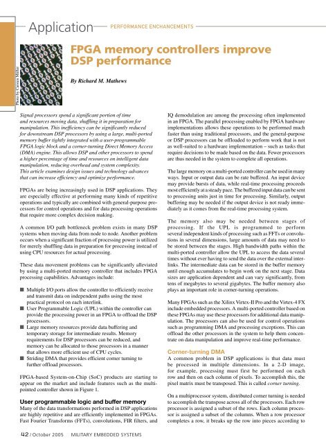
Photo by Carsten Müller<br />
FPGA memory controllers improve<br />
DSP performance<br />
By Richard M. Mathews<br />
Signal processors spend a significant portion of time<br />
and resources moving data, shuffling it in preparation for<br />
manipulation. This inefficiency can be significantly reduced<br />
for downstream DSP processors by using a large, multi-ported<br />
memory buffer tightly integrated with a user-programmable<br />
FPGA logic block and a corner-turning Direct Memory Access<br />
(DMA) engine. This allows DSP and other processors to spend<br />
a higher percentage of time and resources on intelligent data<br />
manipulation, reducing overhead and system complexity.<br />
This article examines design issues and technology advances<br />
that can increase efficiency and optimize performance.<br />
FPGAs are being increasingly used in DSP applications. They<br />
are especially effective at performing many kinds of repetitive<br />
operations and typically are combined with general-purpose processors<br />
for control operations and for data processing operations<br />
that require more complex decision making.<br />
A common I/O path bottleneck problem exists in many DSP<br />
systems when moving data from node to node. Another problem<br />
occurs when a significant fraction of processing power is utilized<br />
for merely shuffling data in preparation for processing instead of<br />
using CPU resources for actual processing.<br />
These data movement problems can be significantly alleviated<br />
by using a multi-ported memory controller that includes FPGA<br />
processing capabilities. Advantages include:<br />
n<br />
n<br />
n<br />
n<br />
Multiple I/O ports allow the controller to efficiently receive<br />
and transmit data on independent paths using the most<br />
practical protocol on each interlink.<br />
User Programmable Logic (UPL) within the controller can<br />
provide the processing power in an FPGA to offload the DSP<br />
processors.<br />
Large memory resources provide data buffering and<br />
temporary storage for intermediate results. Memory<br />
requirements for DSP processors can be reduced, and<br />
memory can be allocated to those processors in a manner<br />
that allows more efficient use of CPU cycles.<br />
Striding DMA that provides efficient corner turning to<br />
further offload processors.<br />
FPGA-based System-on-Chip (SoC) products are starting to<br />
appear on the market and include features such as the multipointed<br />
controller shown in Figure 1.<br />
User programmable logic and buffer memory<br />
Many of the data transformations performed in DSP applications<br />
are highly repetitive and are efficiently implemented in FPGAs.<br />
Fast Fourier Transforms (FFTs), convolutions, FIR filters, and<br />
IQ demodulation are among the processing often implemented<br />
in an FPGA. The parallel processing enabled by FPGA hardware<br />
implementations allows these operations to be performed much<br />
faster than using traditional processors, and the general-purpose<br />
or DSP processors can be offloaded to perform work that is not<br />
as well-suited to a hardware implementation – such as tasks that<br />
require decisions to be made based on the data. Fewer processors<br />
are thus needed in the system to complete all operations.<br />
The large memory on a multi-ported controller can be used in many<br />
ways. Input or output data can be rate buffered. An input device<br />
may provide bursts of data, while real-time processing proceeds<br />
most efficiently at a steady pace. The buffered input data can be sent<br />
to processing units just in time for processing. Similarly, output<br />
buffering may be needed if the output device is not ready immediately<br />
as it comes from the real-time processing system.<br />
The memory also may be needed between stages of<br />
processing. If the UPL is programmed to perform<br />
several independent kinds of processing such as FFTs or convolutions<br />
in several dimensions, large amounts of data may need to<br />
be stored between the stages. High bandwidth paths within the<br />
multi-ported controller allow the UPL to access the data several<br />
times without ever having to send the data over the external interlinks.<br />
The intermediate data can be stored in the buffer memory<br />
until enough accumulates to begin work on the next stage. Data<br />
sizes are application dependent and can vary significantly, from<br />
tens of megabytes to several gigabytes. The buffer memory also<br />
plays an important role in corner-turning operations.<br />
Many FPGAs such as the Xilinx Virtex-II Pro and the Virtex-4 FX<br />
include embedded processors. A multi-ported controller based on<br />
these FPGAs may use these processors for additional data manipulation.<br />
The processors can also be used for control operations<br />
such as programming DMA and processing exceptions. This can<br />
offload the other processors in the system to help them concentrate<br />
on data manipulation and improve real-time performance.<br />
Corner-turning DMA<br />
A common problem in DSP applications is that data must<br />
be processed in multiple dimensions. In a 2-D image,<br />
for example, processing must first be performed on each<br />
row and then on each column of pixels. To accomplish this, the<br />
pixel matrix must be transposed. This is called corner turning.<br />
On a multiprocessor system, distributed corner turning is needed<br />
to accomplish the transpose across all of the processors. Each row<br />
processor is assigned a subset of the rows. Each column processor<br />
is assigned a subset of the columns. When a row processor<br />
completes a row, it breaks up the row into pieces according to<br />
42 / October <strong>2005</strong> <strong>Military</strong> EMBEDDED SYSTEMS