Military Embedded Systems - Fall 2005 - Volume 1 Number 2
Military Embedded Systems - Fall 2005 - Volume 1 Number 2
Military Embedded Systems - Fall 2005 - Volume 1 Number 2

You also want an ePaper? Increase the reach of your titles
YUMPU automatically turns print PDFs into web optimized ePapers that Google loves.
Software Defined Radio<br />
Software<br />
Our representative waveform is connection-oriented, meaning<br />
that for each packet transmitted, an acknowledgement must be<br />
sent indicating whether the packet was successfully<br />
received or not. This acknowledgement is based<br />
on a test of the Cyclic Redundancy Check (CRC)<br />
embedded in the data. The CRC response must<br />
be transmitted 10 μs following the receipt of the<br />
last OFDM symbol, similar to the acknowledgement<br />
time for 802.11g. A hard requirement such as<br />
acknowledgement time will help drive the latency<br />
requirements of our target system.<br />
Step 2: Performing a functional<br />
analysis<br />
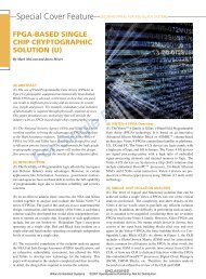
After creating a representative waveform, the next<br />
step in the platform evaluation exercise is to construct<br />
a functional block description of the target<br />
RF Front End<br />
Duplexor<br />
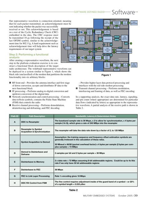
radio architecture. The wideband representative waveform can<br />
be deployed in a system similar to Figure 1, which shows the<br />
black side (unclassified) of the modem that partitions the modem<br />
functionality into six arbitrary blocks:<br />
Course Freq.<br />
Tuning<br />
(RF Front End)<br />
b<br />
Course Freq.<br />
Tuning<br />
(RF Front End)<br />
n<br />
n<br />
Y<br />
Link layer<br />
A/D<br />
Processing<br />
for<br />
Automatic<br />
Gain Control<br />
a<br />
Rx Control<br />
Tx Control<br />
D/A<br />
X<br />
Z<br />
Converter Assembly/<br />
IF Processing<br />
c<br />
processing<br />
Fine Freq.<br />
Tuning<br />
(Digital<br />
Down<br />
Converter)<br />
H<br />
K<br />
Fine Freq.<br />
Tuning<br />
(Digital Up<br />
Converter)<br />
A<br />
Rx Control<br />
Tx Control<br />
N<br />
J<br />
Resampler<br />
Sample<br />
Rate<br />
Control<br />
Sync<br />
Baud<br />
Clock<br />
Sync Control Baud<br />
Clock<br />
Resampler O<br />
Symbol<br />
Staging<br />
Modem Processing<br />
I<br />
B<br />
Demod<br />
Symbol to Bit<br />
C<br />
Symbol<br />
Acquisition<br />
Hop/Frame Sync<br />
Synchronization<br />
Finite<br />
State Machine<br />
(FSM)<br />
P<br />
Mod<br />
Bit to<br />
Symbol<br />
Figure 1<br />
D<br />
Q<br />
L<br />
M<br />
Receive Channel Processing<br />
Deinterleave<br />
& Deframe<br />
E<br />
Memory<br />
Estimated<br />
Baud Clock<br />
Estimated<br />
Carrier<br />
Interleave &<br />
Frame<br />
T<br />
Memory<br />
F<br />
Control<br />
Sample<br />
Clock<br />
Time of Day<br />
R<br />
FEC<br />
Decode<br />
Clock<br />
Generation<br />
(Digital PLLs)<br />
Waveform Control<br />
Network Synchronization<br />
and Control Processing<br />
Transmit Channel Processing<br />
FEC<br />
Encode<br />
G<br />
S<br />
To Link<br />
Layer Processing<br />
U<br />
From<br />
Link Layer<br />
Processing<br />
n<br />
n<br />
n<br />
n<br />
RF front end – Provides the antenna interface and first stage<br />
of down conversion, accepts and distributes IF data to the<br />
next functional block<br />
IF processing – Performs analog-to-digital conversion and<br />
up/down conversion of the digital data<br />
Network synchronization and control processing – Converts<br />
data to/from symbols, contains the Finite State Machine<br />
(FSM) that controls the radio<br />
Receive channel processing – Performs demodulation,<br />
deinterleaving and deframing, and FEC decoding<br />
n<br />
– Provides higher layer data protocol processing and<br />
interfaces with the red-side modem processing<br />
Transmit channel processing – Performs modulation,<br />
interleaving and framing of data, as well as FEC encoding<br />
In a supporting analysis, the exact data rate, latency, signaling,<br />
and pin count (where appropriate) are determined for particular<br />
data flows (indicated by letters) as appropriate to the representative<br />
waveform. A partial analysis of the receive path is shown in<br />
Table 2.<br />
Path ID Path Description Bandwidth, Latency & Determinism Notes<br />
A<br />
DDC to Resampler<br />
The baseband sample rate is 30 Msps, x 2 to allow for synchronization, x 4 bytes per<br />
sample (I & Q), which gives a rate of 240 MBps into the resampler<br />
B<br />
C<br />
D<br />
Resampler to Symbol<br />
Acquisition & Synchronization<br />
Symbol Acquisition to Demod<br />
Demod to Deinterleave and<br />
Deframe<br />
The resampler will take the data rate down by a factor of 2, to 120 MBps<br />
Assumption: the training sequence and frequency offset estimation symbols are<br />
generally irrelevant in the calculation of these rates.<br />
30 Mbaud x 48/80 (packet overhead factor) x 4 bytes per sample (2 bytes per complex<br />
sample) = 72 MBps<br />
2 samples per bit and 2 bytes per sample = 36 Mbps<br />
E<br />
Deinterleave to Memory<br />
2 x data rate = 72 MBps assuming 8-bit addressable regions. Could be up to 4x this<br />
rate if we only have 32 bit addressable regions<br />
F Deinterleave to FEC 36 Mbps<br />
G FEC to Link Layer Processing Rate ½ encoding gives 18 Mbps<br />
H<br />
DDC RX Control from FSM<br />
The fine control requires adjustment inside of the guard band of a symbol – or 20%<br />
of a symbol length = 0.533 µSec<br />
Table 2<br />
<strong>Military</strong> EMBEDDED SYSTEMS October <strong>2005</strong> / 39