Military Embedded Systems - Fall 2005 - Volume 1 Number 2
Military Embedded Systems - Fall 2005 - Volume 1 Number 2
Military Embedded Systems - Fall 2005 - Volume 1 Number 2

You also want an ePaper? Increase the reach of your titles
YUMPU automatically turns print PDFs into web optimized ePapers that Google loves.
Hardware<br />
file to the device resources, one needs to<br />
reverse engineer the FPGA or the FPGA<br />
development software. Some FPGA vendors<br />
do not disclose the configuration<br />
file formats, making reverse engineering<br />
more difficult. With configuration bitstream<br />
encryption, one needs to first find<br />
the key and decrypt the file. It may be<br />
easier and quicker to build a design from<br />
scratch than to reverse engineer a secured<br />
FPGA design.<br />
Tampering is modifying the design stored<br />
in the device or replacing it with a different<br />
design. The tampered device may<br />
contain harmful design code capable of<br />
causing a system to malfunction or steal<br />
sensitive security data. Tampering cannot<br />
be prevented if a volatile key is used<br />
because the key is erasable; once the key is<br />
erased, the device can be configured with<br />
any configuration file. For the nonvolatile<br />
key solution, the device can be set to only<br />
accept configuration files encrypted with<br />
the stored key. A configuration failure signals<br />
possible tampering with the configuration<br />
file during transmission between<br />
the external memory and the FPGA, or<br />
during remotely communicated system<br />
upgrades. This is another advantage of a<br />
nonvolatile key.<br />
Handshaking tokens<br />
Configuration bitstream encryption is only<br />
available in high-density, high-performance<br />
SRAM-based FPGAs. The following<br />
solution allows any FPGA designs to<br />
remain secure against copying, even if the<br />
configuration bitstream is captured. This<br />
is accomplished by disabling the functionality<br />
of a user design within the FPGA<br />
until handshaking tokens are passed to the<br />
FPGA from a secure external device. The<br />
secure external device generates continuous<br />
handshaking tokens to the FPGA to<br />
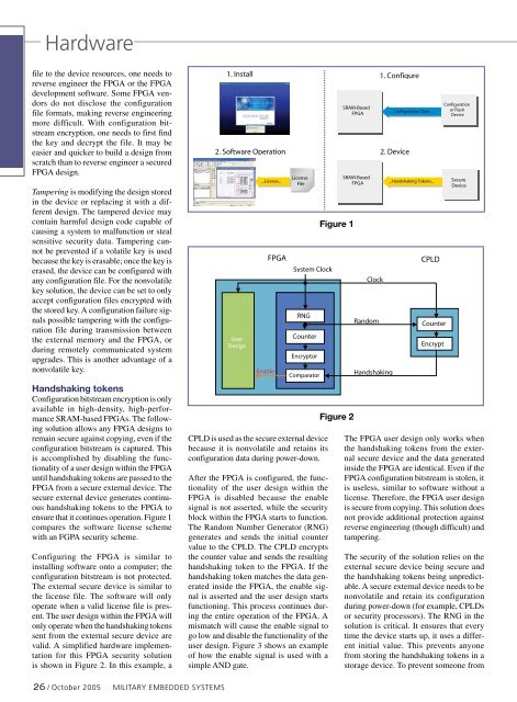
ensure that it continues operation. Figure 1<br />
compares the software license scheme<br />
with an FGPA security scheme.<br />
Configuring the FPGA is similar to<br />
installing software onto a computer; the<br />
configuration bitstream is not protected.<br />
The external secure device is similar to<br />
the license file. The software will only<br />
operate when a valid license file is present.<br />
The user design within the FPGA will<br />
only operate when the handshaking tokens<br />
sent from the external secure device are<br />
valid. A simplified hardware implementation<br />
for this FPGA security solution<br />
is shown in Figure 2. In this example, a<br />
1. Install 1. Configure<br />
2. Software Operation 2. Device<br />
Figure 1. Comparison of Software Figure License 1 Scheme & FPGA Security Scheme<br />
User<br />
Design<br />
...License...<br />
Enable<br />
FPGA<br />
License<br />
File<br />
System Clock<br />
RNG<br />
Counter<br />
Encryptor<br />
Comparator<br />
CPLD is used as the secure external device<br />
because it is nonvolatile and retains its<br />
configuration data during power-down.<br />
After the FPGA is configured, the functionality<br />
of the user design within the<br />
FPGA is disabled because the enable<br />
signal is not asserted, while the security<br />
block within the FPGA starts to function.<br />
The Random <strong>Number</strong> Generator (RNG)<br />
generates and sends the initial counter<br />
value to the CPLD. The CPLD encrypts<br />
the counter value and sends the resulting<br />
handshaking token to the FPGA. If the<br />
handshaking token matches the data generated<br />
inside the FPGA, the enable signal<br />
is asserted and the user design starts<br />
functioning. This process continues during<br />
the entire operation of the FPGA. A<br />
mismatch will cause the enable signal to<br />
go low and disable the functionality of the<br />
user design. Figure 3 shows an example<br />
of how the enable signal is used with a<br />
simple AND gate.<br />
SRAM-Based<br />
FPGA<br />
SRAM-Based<br />
FPGA<br />
... Configuration Data ...<br />
...Handshaking Tokens...<br />
Figure 2. Simplified Hardware Implementation of the FPGA Design Security Solution<br />
Figure 2<br />
Clock<br />
Random<br />
Handshaking<br />
CPLD<br />
Counter<br />
Encrypt<br />
Configuration<br />
or Flash<br />
Device<br />
Secure<br />
Device<br />
The FPGA user design only works when<br />
the handshaking tokens from the external<br />
secure device and the data generated<br />
inside the FPGA are identical. Even if the<br />
FPGA configuration bitstream is stolen, it<br />
is useless, similar to software without a<br />
license. Therefore, the FPGA user design<br />
is secure from copying. This solution does<br />
not provide additional protection against<br />
reverse engineering (though difficult) and<br />
tampering.<br />
The security of the solution relies on the<br />
external secure device being secure and<br />
the handshaking tokens being unpredictable.<br />
A secure external device needs to be<br />
nonvolatile and retain its configuration<br />
during power-down (for example, CPLDs<br />
or security processors). The RNG in the<br />
solution is critical. It ensures that every<br />
time the device starts up, it uses a different<br />
initial value. This prevents anyone<br />
from storing the handshaking tokens in a<br />
storage device. To prevent someone from<br />
26 / October <strong>2005</strong> <strong>Military</strong> EMBEDDED SYSTEMS