Military Embedded Systems - Fall 2005 - Volume 1 Number 2
Military Embedded Systems - Fall 2005 - Volume 1 Number 2
Military Embedded Systems - Fall 2005 - Volume 1 Number 2

You also want an ePaper? Increase the reach of your titles
YUMPU automatically turns print PDFs into web optimized ePapers that Google loves.
Software<br />
Software Defined Radio<br />
Step 3: Mapping to specific processors<br />
After our representative waveform has been created and mapped<br />
to a functional block diagram of the modem, the results need to<br />
be allocated to actual physical processing elements. Notice at this<br />
point a target platform has still not been identified. The functional<br />
blocks should be assigned to specific processor types to estimate<br />
resource utilization that will help determine part sizing, leading<br />
to appropriate hardware platform architectures.<br />
In general, high-speed or computationally intensive algorithms are<br />
mapped to FPGAs, with other algorithms mapped to either a DSP or<br />
a General Purpose Processor (GPP), depending on the anticipated<br />
power utilization and requirements for code portability. Higher<br />
layer back-end processing (link layer, network layer) is typically<br />
performed exclusively on a GPP.<br />
In the case of this representative waveform, the functional processing<br />
blocks described above are mapped into all three different<br />
categories: DSPs, FPGAs, and GPPs. The functional blocks<br />
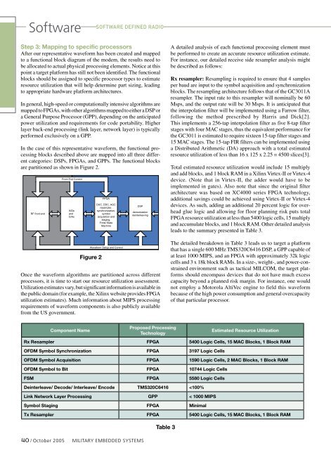
are partitioned as shown in Figure 2.<br />
RF front end<br />
Front End Control<br />
A/Ds<br />
and<br />
D/As<br />
FPGA<br />
DUC, DDC, AGC<br />
resampler,<br />
synchronization,<br />
symbol<br />
acquisition and<br />
staging,<br />
Finite State<br />
Machine<br />
DSP<br />
demodulation<br />
deinterleaving<br />
A detailed analysis of each functional processing element must<br />
be performed to create an accurate resource utilization estimate.<br />
For instance, our detailed receive side resampler analysis might<br />
be described as follows:<br />
Rx resampler: Resampling is required to ensure that 4 samples<br />
per baud are input to the symbol acquisition and synchronization<br />
blocks. The resampling architecture follows that of the GC3011A<br />
resampler. The input rate to this resampler will nominally be 60<br />
Msps, and the output rate will be 30 Msps. It is anticipated that<br />
the interpolation filter will be implemented using a Farrow filter,<br />
following the method prescribed by Harris and Dick[2].<br />
This implements a 256-tap interpolation filter as five 8-tap filter<br />
stages with four MAC stages, thus the equivalent performance for<br />
the GC3011 is estimated to require sixteen 15-tap filter stages and<br />
15 MAC stages. The 15-tap FIR filters can be implemented using<br />
a Distributed Arithmetic (DA) approach with a total estimated<br />
resource utilization of less than 16 x 125 x 2.25 = 4500 slices[3].<br />
Total estimated resource utilization would include 15 multiply<br />
and add blocks, and 1 block RAM in a Xilinx Virtex-II or Virtex-4<br />
device. (Note that in Virtex-II, the adder would have to be<br />
implemented in gates). Also note that since the original filter<br />
architecture was based on XC4000 series FPGA technology,<br />
additional savings could be achieved using Virtex-II or Virtex-4<br />
devices. As such, adding an additional 20 percent logic for overhead<br />
glue logic and allowing for floor planning risk puts total<br />
GPP<br />
link layer<br />
processing FPGA resource utilization at less than 5400 logic cells, 15 multiply<br />
and accumulate blocks, and 1 block RAM. Other detailed analysis<br />
leads to the summary presented in Table 3.<br />
Waveform Setup and Control<br />
Figure 2<br />
Once the waveform algorithms are partitioned across different<br />
processors, it is time to start our resource utilization assessment.<br />
Utilization estimates vary, but significant information is available in<br />
the public domain (for example, the Xilinx website provides FPGA<br />
utilization estimates). Much information about MIPS processing<br />
requirements of waveform components is also publicly available<br />
from the US government.<br />
The detailed breakdown in Table 3 leads us to target a platform<br />
that has a single 600 MHz TMS320C6416 DSP, a GPP capable of<br />
at least 1000 MIPS, and an FPGA with approximately 32k logic<br />
cells and 3 x 18k block RAMs. In a size-, weight-, and power-constrained<br />
environment such as tactical MILCOM, the target platforms<br />
should encompass devices that do not have much excess<br />
capacity beyond a planned risk margin. For instance, one would<br />
not employ a Motorola AltiVec engine to field this waveform<br />
because of the high power consumption and general overcapacity<br />
of that particular processor.<br />
Modem Channel Processing<br />
Component Name<br />
40 / October <strong>2005</strong> <strong>Military</strong> EMBEDDED SYSTEMS<br />
Proposed Processing<br />
Technology<br />
Estimated Resource Utilization<br />
Rx Resampler FPGA 5400 Logic Cells, 15 MAC Blocks, 1 Block RAM<br />
OFDM Symbol Synchronization FPGA 3197 Logic Cells<br />
OFDM Symbol Acquisition FPGA 1590 Logic Cells, 2 MAC Blocks, 1 Block RAM<br />
OFDM Symbol to Bit FPGA 10744 Logic Cells<br />
FSM FPGA 5580 Logic Cells<br />
Deinterleave/ Decode/ Interleave/ Encode TMS320C6416