ADSP-21061/ADSP-21061L
ADSP-21061/ADSP-21061L
ADSP-21061/ADSP-21061L

You also want an ePaper? Increase the reach of your titles
YUMPU automatically turns print PDFs into web optimized ePapers that Google loves.
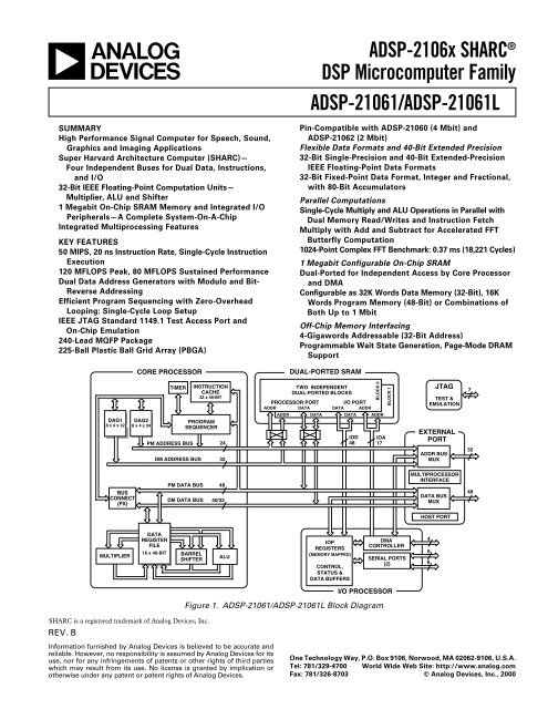
aSUMMARYHigh Performance Signal Computer for Speech, Sound,Graphics and Imaging ApplicationsSuper Harvard Architecture Computer (SHARC)—Four Independent Buses for Dual Data, Instructions,and I/O32-Bit IEEE Floating-Point Computation Units—Multiplier, ALU and Shifter1 Megabit On-Chip SRAM Memory and Integrated I/OPeripherals—A Complete System-On-A-ChipIntegrated Multiprocessing FeaturesKEY FEATURES50 MIPS, 20 ns Instruction Rate, Single-Cycle InstructionExecution120 MFLOPS Peak, 80 MFLOPS Sustained PerformanceDual Data Address Generators with Modulo and Bit-Reverse AddressingEfficient Program Sequencing with Zero-OverheadLooping: Single-Cycle Loop SetupIEEE JTAG Standard 1149.1 Test Access Port andOn-Chip Emulation240-Lead MQFP Package225-Ball Plastic Ball Grid Array (PBGA)CORE PROCESSOR<strong>ADSP</strong>-2106x SHARC®DSP Microcomputer Family<strong>ADSP</strong>-<strong>21061</strong>/<strong>ADSP</strong>-<strong>21061</strong>LPin-Compatible with <strong>ADSP</strong>-21060 (4 Mbit) and<strong>ADSP</strong>-21062 (2 Mbit)Flexible Data Formats and 40-Bit Extended Precision32-Bit Single-Precision and 40-Bit Extended-PrecisionIEEE Floating-Point Data Formats32-Bit Fixed-Point Data Format, Integer and Fractional,with 80-Bit AccumulatorsParallel ComputationsSingle-Cycle Multiply and ALU Operations in Parallel withDual Memory Read/Writes and Instruction FetchMultiply with Add and Subtract for Accelerated FFTButterfly Computation1024-Point Complex FFT Benchmark: 0.37 ms (18,221 Cycles)1 Megabit Configurable On-Chip SRAMDual-Ported for Independent Access by Core Processorand DMAConfigurable as 32K Words Data Memory (32-Bit), 16KWords Program Memory (48-Bit) or Combinations ofBoth Up to 1 MbitOff-Chip Memory Interfacing4-Gigawords Addressable (32-Bit Address)Programmable Wait State Generation, Page-Mode DRAMSupportDUAL-PORTED SRAMDAG18 x 4 x 32DAG28 x 4 x 24TIMERPM ADDRESS BUSDM ADDRESS BUSINSTRUCTIONCACHE32 x 48-BITPROGRAMSEQUENCER2432TWO INDEPENDENTDUAL-PORTED BLOCKSPROCESSOR PORT I/O PORTADDR DATA DATA ADDRADDR DATA DATA ADDRIOD48BLOCK 0IOA17BLOCK 1JTAGTEST &EMULATIONEXTERNALPORTADDR BUSMUX732BUSCONNECT(PX)PM DATA BUSDM DATA BUS4840/32MULTIPROCESSORINTERFACEDATA BUSMUX48HOST PORTMULTIPLIERDATAREGISTERFILE16 x 40-BIT BARRELSHIFTERALUIOPREGISTERS(MEMORY MAPPED)CONTROL,STATUS &DATA BUFFERSI/O PROCESSORFigure 1. <strong>ADSP</strong>-<strong>21061</strong>/<strong>ADSP</strong>-<strong>21061</strong>L Block DiagramDMACONTROLLERSERIAL PORTS(2)466SHARC is a registered trademark of Analog Devices, Inc.REV. BInformation furnished by Analog Devices is believed to be accurate andreliable. However, no responsibility is assumed by Analog Devices for itsuse, nor for any infringements of patents or other rights of third partieswhich may result from its use. No license is granted by implication orotherwise under any patent or patent rights of Analog Devices.One Technology Way, P.O. Box 9106, Norwood, MA 02062-9106, U.S.A.Tel: 781/329-4700 World Wide Web Site: http://www.analog.comFax: 781/326-8703 © Analog Devices, Inc., 2000
<strong>ADSP</strong>-<strong>21061</strong>/<strong>ADSP</strong>-<strong>21061</strong>LDMA Controller6 DMA ChannelsBackground DMA Transfers at 50 MHz, in Parallel withFull-Speed Processor ExecutionPerforms Transfers Between <strong>ADSP</strong>-<strong>21061</strong> Internal Memoryand External Memory, External Peripherals, HostProcessor, or Serial PortsHost Processor InterfaceEfficient Interface to 16- and 32-Bit MicroprocessorsHost can Directly Read/Write <strong>ADSP</strong>-<strong>21061</strong> Internal MemoryMultiprocessingGlueless Connection for Scalable DSP MultiprocessingArchitectureDistributed On-Chip Bus Arbitration for Parallel BusConnect of Up To Six <strong>ADSP</strong>-<strong>21061</strong>s Plus Host300 Mbytes/s Transfer Rate Over Parallel BusSerial PortsTwo 40 Mbit/s Synchronous Serial PortsIndependent Transmit and Receive Functions3- to 32-Bit Data Word Width-Law/A-Law Hardware CompandingTDM Multichannel ModeMultichannel Signaling ProtocolTABLE OF CONTENTSGENERAL DESCRIPTION . . . . . . . . . . . . . . . . . . . . . . . . . 3<strong>ADSP</strong>-21000 FAMILY CORE ARCHITECTURE . . . . . . . 4<strong>ADSP</strong>-<strong>21061</strong> FEATURES . . . . . . . . . . . . . . . . . . . . . . . . . . 4DEVELOPMENT TOOLS . . . . . . . . . . . . . . . . . . . . . . . . . . 8ADDITIONAL INFORMATION . . . . . . . . . . . . . . . . . . . . . 8PIN DESCRIPTIONS . . . . . . . . . . . . . . . . . . . . . . . . . . . . . 9TARGET BOARD CONNECTOR FOR EZ-ICE ®PROBE . . . . . . . . . . . . . . . . . . . . . . . . . . . . . . . . . . . . . . 12RECOMMENDED OPERATING CONDITIONS (5 V) . 14ELECTRICAL CHARACTERISTICS (5 V) . . . . . . . . . . . 14POWER DISSIPATION <strong>ADSP</strong>-<strong>21061</strong> (5 V) . . . . . . . . . . . . 15RECOMMENDED OPERATING CONDITIONS (3.3 V) 16ELECTRICAL CHARACTERISTICS (3.3 V) . . . . . . . . . . 16POWER DISSIPATION <strong>ADSP</strong>-<strong>21061</strong>L (3.3 V) . . . . . . . . . 17ABSOLUTE MAXIMUM RATINGS . . . . . . . . . . . . . . . . 18TIMING SPECIFICATIONS . . . . . . . . . . . . . . . . . . . . . . . 18Memory Read—Bus Master . . . . . . . . . . . . . . . . . . . . . . . 21Memory Write—Bus Master . . . . . . . . . . . . . . . . . . . . . . 22Synchronous Read/Write—Bus Master . . . . . . . . . . . . . . 23Synchronous Read/Write—Bus Slave . . . . . . . . . . . . . . . . 25Multiprocessor Bus Request and Host Bus Request . . . . . 26Asynchronous Read/Write—Host to <strong>ADSP</strong>-<strong>21061</strong> . . . . . . 28Three-State Timing—Bus Master, Bus Slave,HBR, SBTS . . . . . . . . . . . . . . . . . . . . . . . . . . . . . . . . . 30DMA Handshake . . . . . . . . . . . . . . . . . . . . . . . . . . . . . . . 32Serial Ports . . . . . . . . . . . . . . . . . . . . . . . . . . . . . . . . . . . . 34JTAG Test Access Port and Emulation . . . . . . . . . . . . . . . 37OUTPUT DRIVE CURRENTS . . . . . . . . . . . . . . . . . . . . . 38POWER DISSIPATION . . . . . . . . . . . . . . . . . . . . . . . . . . . 38TEST CONDITIONS . . . . . . . . . . . . . . . . . . . . . . . . . . . . 38ENVIRONMENTAL CONDITIONS . . . . . . . . . . . . . . . . 41240-LEAD METRIC MQFP PIN CONFIGURATIONS . . 42OUTLINE DIMENSIONS . . . . . . . . . . . . . . . . . . . . . . 43, 44<strong>ADSP</strong>-<strong>21061</strong>L 225-Ball Plastic Ball Grid Array (PBGA)Package Pinout . . . . . . . . . . . . . . . . . . . . . . . . . . . . . . . . . 45225-Ball Plastic Ball Grid Array (PBGA) Package Pinout . . . . . 46OUTLINE DIMENSIONS . . . . . . . . . . . . . . . . . . . . . . . . . 47ORDERING GUIDE . . . . . . . . . . . . . . . . . . . . . . . . . . . . . 47FIGURESFigure 1. <strong>ADSP</strong>-<strong>21061</strong>/<strong>ADSP</strong>-<strong>21061</strong>L Block Diagram . . . . 1Figure 2. <strong>ADSP</strong>-<strong>21061</strong>/<strong>ADSP</strong>-<strong>21061</strong>L System . . . . . . . . . . . 4Figure 3. Multiprocessing System . . . . . . . . . . . . . . . . . . . . . 6Figure 4. <strong>ADSP</strong>-<strong>21061</strong>/<strong>ADSP</strong>-<strong>21061</strong>L Memory Map . . . . . 7Figure 5. Target Board Connector For <strong>ADSP</strong>-<strong>21061</strong>/EZ-ICE is a registered trademark of Analog Devices, Inc.–2–<strong>ADSP</strong>-<strong>21061</strong>L EZ-ICE Emulator (Jumpers in Place) . . . 12Figure 6. JTAG Scan Path Connections for Multiple<strong>ADSP</strong>-<strong>21061</strong>/<strong>ADSP</strong>-<strong>21061</strong>L Systems . . . . . . . . . . . . . . . 12Figure 7. JTAG Clocktree for Multiple <strong>ADSP</strong>-<strong>21061</strong>/<strong>ADSP</strong>-<strong>21061</strong>L Systems . . . . . . . . . . . . . . . . . . . . . . . . . . 13Figure 8. Clock Input . . . . . . . . . . . . . . . . . . . . . . . . . . . . . 19Figure 9. Reset . . . . . . . . . . . . . . . . . . . . . . . . . . . . . . . . . . 19Figure 10. Interrupts . . . . . . . . . . . . . . . . . . . . . . . . . . . . . . 20Figure 11. Timer . . . . . . . . . . . . . . . . . . . . . . . . . . . . . . . . 20Figure 12. Flags . . . . . . . . . . . . . . . . . . . . . . . . . . . . . . . . . 20Figure 13. Memory Read—Bus Master . . . . . . . . . . . . . . . . 21Figure 14. Memory Write—Bus Master . . . . . . . . . . . . . . . 22Figure 15. Synchronous Read/Write—Bus Master . . . . . . . 24Figure 16. Synchronous Read/Write—Bus Slave . . . . . . . . . 25Figure 17. Multiprocessor Bus Request and Host BusRequest . . . . . . . . . . . . . . . . . . . . . . . . . . . . . . . . . . . . . . 27Figure 18a. Synchronous REDY Timing . . . . . . . . . . . . . . 28Figure 18b. Asynchronous Read/Write—Host to<strong>ADSP</strong>-<strong>21061</strong>/<strong>ADSP</strong>-<strong>21061</strong>L . . . . . . . . . . . . . . . . . . . . . . 29Figure 19a. Three-State Timing (Bus Transition Cycle,SBTS Assertion) . . . . . . . . . . . . . . . . . . . . . . . . . . . . . . . 31Figure 19b. Three-State Timing (Host Transition Cycle) . . 31Figure 20. DMA Handshake Timing . . . . . . . . . . . . . . . . . 33Figure 21. Serial Ports . . . . . . . . . . . . . . . . . . . . . . . . . . . . 35Figure 22. External Late Frame Sync . . . . . . . . . . . . . . . . . 36Figure 23. JTAG Test Access Port and Emulation . . . . . . . 37Figure 24. Output Enable/Disable . . . . . . . . . . . . . . . . . . . 39Figure 25. Equivalent Device Loading for AC Measurements(Includes All Fixtures) . . . . . . . . . . . . . . . . . . . . . . . . . . . 39Figure 26. Voltage Reference Levels for AC Measurements(Except Output Enable/Disable) . . . . . . . . . . . . . . . . . . . . 39Figure 27. <strong>ADSP</strong>-2106x Typical Drive Currents(V DD = 5 V) . . . . . . . . . . . . . . . . . . . . . . . . . . . . . . . . . . . 40Figure 28. Typical Output Rise Time (10%–90% V DD ) vs.Load Capacitance (V DD = 5 V) . . . . . . . . . . . . . . . . . . . . 40Figure 29. Typical Output Rise Time (0.8 V–2.0 V) vs. LoadCapacitance (V DD = 5 V) . . . . . . . . . . . . . . . . . . . . . . . . . 40Figure 30. Typical Output Delay or Hold vs. Load Capacitance(at Maximum Case Temperature) (V DD = 5 V) . . . . . . . . 40Figure 31. <strong>ADSP</strong>-2106x Typical Drive Currents(V DD = 3.3 V) . . . . . . . . . . . . . . . . . . . . . . . . . . . . . . . . . . 40Figure 32. Typical Output Rise Time (10%–90% V DD ) vs.Load Capacitance (V DD = 3.3 V) . . . . . . . . . . . . . . . . . . . 40Figure 33. Typical Output Rise Time (0.8 V–2.0 V) vs. LoadCapacitance (V DD = 3.3 V) . . . . . . . . . . . . . . . . . . . . . . . 41Figure 34. Typical Output Delay or Hold vs. Load Capacitance(at Maximum Case Temperature) (V DD = 3.3 V) . . . . . . . 41REV. B
S ®<strong>ADSP</strong>-<strong>21061</strong>/<strong>ADSP</strong>-<strong>21061</strong>LGENERAL NOTEThis data sheet represents production released specificationsfor the <strong>ADSP</strong>-<strong>21061</strong> 5 V and <strong>ADSP</strong>-<strong>21061</strong>L 3.3 V processors.<strong>ADSP</strong>-<strong>21061</strong> is used throughout this data sheet to refer toboth devices unless expressly noted.GENERAL DESCRIPTIONThe <strong>ADSP</strong>-<strong>21061</strong> is a member of the powerful SHARC familyof floating point processors. The SHARC—Super HarvardArchitecture Computer—are signal processing microcomputersthat offer new capabilities and levels of integration and performance.The <strong>ADSP</strong>-<strong>21061</strong> is a 32-bit processor optimized forhigh performance DSP applications. The <strong>ADSP</strong>-<strong>21061</strong> combinesthe <strong>ADSP</strong>-21000 DSP core with a dual-ported on-chipSRAM and an I/O processor with a dedicated I/O bus to form acomplete system-in-a-chip.Fabricated in a high-speed, low-power CMOS process, the<strong>ADSP</strong>-<strong>21061</strong> has a 20 ns instruction cycle time operating at upto 50 MIPS. With its on-chip instruction cache, the processor canexecute every instruction in a single cycle. Table I shows performancebenchmarks for the <strong>ADSP</strong>-<strong>21061</strong>/<strong>ADSP</strong>-<strong>21061</strong>L.The <strong>ADSP</strong>-<strong>21061</strong> SHARC combines a high-performance floating-pointDSP core with integrated, on-chip system features,including a 1 Mbit SRAM memory, host processor interface,DMA controller, serial ports and parallel bus connectivity forglueless DSP multiprocessing.Figure 1 shows a block diagram of the <strong>ADSP</strong>-<strong>21061</strong>/<strong>ADSP</strong>-<strong>21061</strong>L, illustrating the following architectural features:Computation Units (ALU, Multiplier and Shifter) with aShared Data Register FileData Address Generators (DAG1, DAG2)Program Sequencer with Instruction CacheInterval Timer1 Mbit On-Chip SRAMExternal Port for Interfacing to Off-Chip Memory andPeripheralsHost Port & Multiprocessor InterfaceDMA ControllerSerial PortsJTAG Test Access PortFigure 2 shows a typical single-processor system. A multiprocessingsystem is shown in Figure 3.Table I. <strong>ADSP</strong>-<strong>21061</strong>/<strong>ADSP</strong>-<strong>21061</strong>L Benchmarks (@ 50 MHz)1024-Pt. Complex FFT 0.37 ms 18,221 Cycles(Radix 4, with Digit Reverse)FIR Filter (per Tap) 20 ns 1 CycleIIR Filter (per Biquad) 80 ns 4 CyclesDivide (y/x) 120 ns 6 CyclesInverse Square Root (1/√x) 180 ns 9 CyclesDMA Transfer Rate300 Mbytes/sREV. B–3–
<strong>ADSP</strong>-<strong>21061</strong>/<strong>ADSP</strong>-<strong>21061</strong>L<strong>ADSP</strong>-2106x #6<strong>ADSP</strong>-2106x #5<strong>ADSP</strong>-2106x #4<strong>ADSP</strong>-2106x #3CONTROLADDRESSDATACLKINADDR 31-0RESETDATA 47-0RPBA3011 ID 2-0CONTROLCPABR 1-2 , BR 4-6BR 35<strong>ADSP</strong>-2106x #2CLKINADDR 31-0RESETDATA 47-05RPBA3010 ID 2-0CONTROLCPABR 1 , BR 3-6BR 21xCLOCKRESET0013<strong>ADSP</strong>-2106x #1CLKINRESETRPBAID 2-0ADDR 31-0DATA 47-0RDWRACKMS 3-0CONTROLADDRESSDATAADDRDATAOEWEACKCSGLOBALMEMORYANDPERIPHERALS(OPTIONAL)CONTROLBMSPAGESBTSSWADRCLKCSHBRHBGREDYCPABR 2-6BR 15CSADDRDATABOOTEPROM(OPTIONAL)HOSTPROCESSORINTERFACE(OPTIONAL)ADDRDATAFigure 3. Multiprocessing System–6–REV. B
<strong>ADSP</strong>-<strong>21061</strong>/<strong>ADSP</strong>-<strong>21061</strong>LINTERNALMEMORYSPACEMULTIPROCESSORMEMORY SPACEIOP REGISTERSNORMAL WORD ADDRESSINGSHORT WORD ADDRESSINGINTERNAL MEMORY SPACEOF <strong>ADSP</strong>-2106xWITH ID=001INTERNAL MEMORY SPACEOF <strong>ADSP</strong>-2106xWITH ID=010INTERNAL MEMORY SPACEOF <strong>ADSP</strong>-2106xWITH ID=011INTERNAL MEMORY SPACEOF <strong>ADSP</strong>-2106xWITH ID=100INTERNAL MEMORY SPACEOF <strong>ADSP</strong>-2106xWITH ID=101INTERNAL MEMORY SPACEOF <strong>ADSP</strong>-2106xWITH ID=110BROADCAST WRITETO ALL<strong>ADSP</strong>-2106xs0x0000 00000x0002 00000x0004 00000x0008 00000x0010 00000x0018 00000x0020 00000x0028 00000x0030 00000x0038 00000x003F FFFFEXTERNALMEMORYSPACEBANK 0DRAM(OPTIONAL)BANK 1BANK 2BANK 3NONBANKED0x0040 0000MS 0MS 1MS 2MS 3BANK SIZE ISSELECTED BYMSIZE BIT FIELD OFSYSCONREGISTER.NORMAL WORD ADDRESSING: 32-BIT DATA WORDS48-BIT INSTRUCTION WORDSSHORT WORD ADDRESSING: 16-BIT DATA WORDS0xFFFF FFFFFigure 4. <strong>ADSP</strong>-<strong>21061</strong>/<strong>ADSP</strong>-<strong>21061</strong>L Memory MapREV. B–7–
<strong>ADSP</strong>-<strong>21061</strong>/<strong>ADSP</strong>-<strong>21061</strong>LPorting Code from <strong>ADSP</strong>-21060 or <strong>ADSP</strong>-21062 to the<strong>ADSP</strong>-<strong>21061</strong>The <strong>ADSP</strong>-<strong>21061</strong> is pin compatible with the <strong>ADSP</strong>-21060/<strong>ADSP</strong>-<strong>21061</strong>/<strong>ADSP</strong>-21062 processors. The <strong>ADSP</strong>-<strong>21061</strong> pinsthat correspond to the Link Port pins of the <strong>ADSP</strong>-21060/<strong>ADSP</strong>-21062 are no-connects.The <strong>ADSP</strong>-<strong>21061</strong> is object code compatible with the <strong>ADSP</strong>-21060/<strong>ADSP</strong>-21062 except for the following functionalchanges:The <strong>ADSP</strong>-<strong>21061</strong> memory is organized into two blockswith eight columns that are 4K deep per block. The<strong>ADSP</strong>-21060/<strong>ADSP</strong>-21062 memory has 16 columns per block.Link port functions are not available.Handshake external port DMA pins DMAR2 and DMAG2are assigned to external port DMA Channel 6 instead ofChannel 8.2-D DMA capability of the SPORT is not available.The modify registers in SPORT DMA are not programmable.On the <strong>ADSP</strong>-<strong>21061</strong>, Block 0 starts at the beginning of internalmemory, normal word address 0x0002 0000. Block 1 starts atthe end of Block 0, with contiguous addresses. The remainingaddresses in internal memory are divided into blocks that aliasinto Block 1. This allows any code or data stored in Block 1 onthe <strong>ADSP</strong>-21062 to retain the same addresses on the <strong>ADSP</strong>-<strong>21061</strong>—these addresses will alias into the actual Block 1 of eachprocessor.If you develop your application using the <strong>ADSP</strong>-21062, but willmigrate to the <strong>ADSP</strong>-<strong>21061</strong>, use only the first eight columns ofeach memory bank. Limit your application to 8K of instructionsor up to 16K of data in each bank of the <strong>ADSP</strong>-21062, or anycombinations of instructions or data that does not exceed thememory bank.DEVELOPMENT TOOLSThe <strong>ADSP</strong>-<strong>21061</strong> is supported with a complete set of softwareand hardware development tools, including an EZ-ICE In-Circuit Emulator, EZ-Kit Lite, and development software. TheSHARC EZ-Kit Lite (ADDS-2106x-EZ-Lite) is a complete lowcost package for DSP evaluation and prototyping. The EZ-KitLite contains an evaluation board with an <strong>ADSP</strong>-<strong>21061</strong> (5 V)processor and provides a serial connection to your PC. The EZ-Kit Lite also includes an optimizing compiler, assembler, instructionlevel simulator, run-time libraries, diagnostic utilitiesand a complete set of example programs.The same EZ-ICE hardware can be used for the <strong>ADSP</strong>-21060/<strong>ADSP</strong>-21062, to fully emulate the <strong>ADSP</strong>-<strong>21061</strong>, with the exceptionof displaying and modifying the two new SPORTSregisters. The emulator will not display these two registers,but your code can use them.Analog Devices <strong>ADSP</strong>-21000 Family Development Softwareincludes an easy to use Assembler based on an algebraic syntax,Assembly Library/Librarian, Linker, instruction-level Simulator,an ANSI C optimizing Compiler, the CBUG C Source—Level Debugger and a C Runtime Library including DSP andmathematical functions. The Optimizing Compiler includesNumerical C extensions based on the work of the ANSI NumericalC Extensions Group. Numerical C provides extensionsto the C language for array selections, vector math operations,complex data types, circular pointers and variably dimensionedarrays. The <strong>ADSP</strong>-21000 Family Development Software isavailable for both the PC and Sun platforms.The EZ-ICE Emulator uses the IEEE 1149.1 JTAG test accessport of the <strong>ADSP</strong>-<strong>21061</strong> processor to monitor and control thetarget board processor during emulation. The EZ-ICE providesfull-speed emulation, allowing inspection and modification ofmemory, registers, and processor stacks. Nonintrusive in-circuitemulation is assured by the use of the processor’s JTAG interface—theemulator does not affect target system loading ortiming.Further details and ordering information are available in the<strong>ADSP</strong>-21000 Family Hardware and Software Development Toolsdata sheet (ADDS-210xx-TOOLS). This data sheet can berequested from any Analog Devices sales office or distributor.In addition to the software and hardware development toolsavailable from Analog Devices, third parties provide a widerange of tools supporting the SHARC processor family. Hardwaretools include SHARC PC plug-in cards multiprocessorSHARC VME boards, and daughter and modules with multipleSHARCs and additional memory. These modules are based onthe SHARCPAC module specification. Third Party softwaretools include an Ada compiler, DSP libraries, operating systemsand block diagram design tools.ADDITIONAL INFORMATIONThis data sheet provides a general overview of the <strong>ADSP</strong>-<strong>21061</strong>architecture and functionality. For detailed information on the<strong>ADSP</strong>-21000 Family core architecture and instruction set, refer tothe <strong>ADSP</strong>-2106x SHARC User’s Manual, Second Edition.CBUG and SHARCPAC are trademarks of Analog Devices, Inc.–8–REV. B
<strong>ADSP</strong>-<strong>21061</strong>/<strong>ADSP</strong>-<strong>21061</strong>LPIN DESCRIPTIONS<strong>ADSP</strong>-<strong>21061</strong> pin definitions are listed below. Inputs identifiedas synchronous (S) must meet timing requirements with respectto CLKIN (or with respect to TCK for TMS, TDI). Inputsidentified as asynchronous (A) can be asserted asynchronouslyto CLKIN (or to TCK for TRST).Unused inputs should be tied or pulled to IVDD or IGND,except for ADDR 31-0 , DATA 47-0 , FLAG 3-0 , SW and inputs thathave internal pull-up or pull-down resistors (CPA, ACK, DTx,DRx, TCLKx, RCLKx, TMS and TDI)—these pins can be leftfloating. These pins have a logic-level hold circuit that preventsthe input from floating internally.I = Input S = Synchronous P = Power Supply(O/D) = Open Drain O = Output A = AsynchronousG = Ground (A/D) = Active DriveT = Three-State (when SBTS is asserted, or when the<strong>ADSP</strong>-2106x is a bus slave)Pin Type FunctionPIN FUNCTION DESCRIPTIONSADDR 31-0 I/O/T External Bus Address. The <strong>ADSP</strong>-<strong>21061</strong> outputs addresses for external memory and peripheralson these pins. In a multiprocessor system the bus master outputs addresses for read/writes of theinternal memory or IOP registers of other <strong>ADSP</strong>-2106xs. The <strong>ADSP</strong>-<strong>21061</strong> inputs addresses when ahost processor or multiprocessing bus master is reading or writing its internal memory or IOP registers.DATA 47-0 I/O/T External Bus Data. The <strong>ADSP</strong>-<strong>21061</strong> inputs and outputs data and instructions on these pins.The external data bus transfers 32-bit single-precision floating-point data and 32-bit fixed-pointdata over Bits 47-16. 40-bit extended-precision floating-point data is transferred over Bits 47-8 ofthe bus. 16-bit short word data is transferred over Bits 31-16 of the bus. Pull-up resistors on unusedDATA pins are not necessary.MS 3-0 O/T Memory Select Lines. These lines are asserted (low) as chip selects for the corresponding banksof external memory. Memory bank size must be defined in the <strong>ADSP</strong>-<strong>21061</strong>’s system control register(SYSCON). The MS 3-0 lines are decoded memory address lines that change at the same time asthe other address lines. When no external memory access is occurring the MS 3-0 lines are inactive;they are active, however, when a conditional memory access instruction is executed, whether or not thecondition is true. MS 0 can be used with the PAGE signal to implement a bank of DRAM memory(Bank 0). In a multiprocessor system the MS 3-0 lines are output by the bus master.RD I/O/T Memory Read Strobe. This pin is asserted (low) when the <strong>ADSP</strong>-<strong>21061</strong> reads from externalmemory devices or from the internal memory of other <strong>ADSP</strong>-<strong>21061</strong>s. External devices (includingother <strong>ADSP</strong>-<strong>21061</strong>s) must assert RD to read from the <strong>ADSP</strong>-<strong>21061</strong>’s internal memory. In a multiprocessorsystem RD is output by the bus master and is input by all other <strong>ADSP</strong>-<strong>21061</strong>s.WR I/O/T Memory Write Strobe. This pin is asserted (low) when the <strong>ADSP</strong>-<strong>21061</strong> writes to external memorydevices or to the internal memory of other <strong>ADSP</strong>-<strong>21061</strong>s. External devices must assert WR to write tothe <strong>ADSP</strong>-<strong>21061</strong>’s internal memory. In a multiprocessor system WR is output by the bus master and isinput by all other <strong>ADSP</strong>-<strong>21061</strong>s.PAGE O/T DRAM Page Boundary. The <strong>ADSP</strong>-<strong>21061</strong> asserts this pin to signal that an external DRAM pageboundary has been crossed. DRAM page size must be defined in the <strong>ADSP</strong>-<strong>21061</strong>’s memory controlregister (WAIT). DRAM can only be implemented in external memory Bank 0; the PAGEsignal can only be activated for Bank 0 accesses. In a multiprocessor system PAGE is output by thebus master.ADRCLK O/T Address Clock for synchronous external memories. Addresses on ADDR 31-0 are valid before therising edge of ADRCLK. In a multiprocessing system ADRCLK is output by the bus master.SW I/O/T Synchronous Write Select. This signal is used to interface the <strong>ADSP</strong>-2106x to synchronous memorydevices (including other <strong>ADSP</strong>-<strong>21061</strong>s). The <strong>ADSP</strong>-<strong>21061</strong> asserts SW (low) to provide an early indicationof an impending write cycle, which can be aborted if WR is not later asserted (e.g. in a conditionalwrite instruction). In a multiprocessor system, SW is output by the bus master and is input by all other<strong>ADSP</strong>-<strong>21061</strong>s to determine if the multiprocessor memory access is a read or write. SW is asserted at thesame time as the address output. A host processor using synchronous writes must assert this pin whenwriting to the <strong>ADSP</strong>-<strong>21061</strong>(s).ACK I/O/S Memory Acknowledge. External devices can deassert ACK (low) to add wait states to an externalmemory access. ACK is used by I/O devices, memory controllers or other peripherals to hold offcompletion of an external memory access. The <strong>ADSP</strong>-<strong>21061</strong> deasserts ACK as an output to addwait states to a synchronous access of its internal memory. In a multiprocessor system, a slave<strong>ADSP</strong>-<strong>21061</strong> deasserts the bus master’s ACK input to add wait state(s) to an access of its internalmemory. The bus master has a keeper latch on its ACK pin that maintains the input at the level itwas last driven to.REV. B–9–
<strong>ADSP</strong>-<strong>21061</strong>/<strong>ADSP</strong>-<strong>21061</strong>LPin Type FunctionSBTS I/S Suspend Bus Three-State. External devices can assert SBTS (low) to place the external bus address,data, selects, and strobes in a high impedance state for the following cycle. If the <strong>ADSP</strong>-<strong>21061</strong>attempts to access external memory while SBTS is asserted, the processor will halt and the memoryaccess will not be completed until SBTS is deasserted. SBTS should only be used to recover fromPAGE faults or host processor/<strong>ADSP</strong>-<strong>21061</strong> deadlock.IRQ 2-0 I/A Interrupt Request Lines. May be either edge-triggered or level-sensitive.FLAG 3-0 I/O/A Flag Pins. Each is configured via control bits as either an input or an output. As an input, it can betested as a condition. As an output, it can be used to signal external peripherals.TIMEXP O Timer Expired. Asserted for four cycles when the timer is enabled and TCOUNT decrements tozero.HBR I/A Host Bus Request. Must be asserted by a host processor to request control of the <strong>ADSP</strong>-<strong>21061</strong>’sexternal bus. When HBR is asserted in a multiprocessing system, the <strong>ADSP</strong>-<strong>21061</strong> that is bus masterwill relinquish the bus and assert HBG. To relinquish the bus, the <strong>ADSP</strong>-<strong>21061</strong> places the address,data, select, and strobe lines in a high impedance state. HBR has priority over all <strong>ADSP</strong>-<strong>21061</strong> busrequests (BR 6-1 ) in a multiprocessing system.HBG I/O Host Bus Grant. Acknowledges an HBR bus request, indicating that the host processor may takecontrol of the external bus. HBG is asserted (held low) by the <strong>ADSP</strong>-<strong>21061</strong> until HBR is released. In amultiprocessing system, HBG is output by the <strong>ADSP</strong>-<strong>21061</strong> bus master and is monitored by all others.CS I/A Chip Select. Asserted by host processor to select the <strong>ADSP</strong>-<strong>21061</strong>.REDY (O/D) O Host Bus Acknowledge. The <strong>ADSP</strong>-2106x deasserts REDY (low) to add wait states to an asynchronousaccess of its internal memory or IOP registers by a host. Open drain output (O/D) by default; canbe programmed in ADREDY bit of SYSCON register to be active drive (A/D). REDY will only beoutput if the CS and HBR inputs are asserted.DMAR1 I/A DMA Request 1 (DMA Channel 7).DMAR2 I/A DMA Request 2 (DMA Channel 6).DMAG1 O/T DMA Grant 1 (DMA Channel 7).DMAG2 O/T DMA Grant 2 (DMA Channel 6).BR 6-1 I/O/S Multiprocessing Bus Requests. Used by multiprocessing <strong>ADSP</strong>-<strong>21061</strong>s to arbitrate for bus mastership.An <strong>ADSP</strong>-<strong>21061</strong> only drives its own BRx line (corresponding to the value of its ID 2-0 inputs) andmonitors all others. In a multiprocessor system with less than six <strong>ADSP</strong>-<strong>21061</strong>s, the unused BRx pinsshould be tied high; the processor’s own BRx line must not be tied high or low because it is an output.ID 2-0 I Multiprocessing ID. Determines which multiprocessing bus request (BR1–BR6) is used by <strong>ADSP</strong>-<strong>21061</strong>. ID = 001 corresponds to BR1, ID = 010 corresponds to BR2, etc. ID = 000 in single-processorsystems. These lines are a system configuration selection which should be hardwired or only changed atreset.RPBA I/S Rotating Priority Bus Arbitration Select. When RPBA is high, rotating priority for multiprocessorbus arbitration is selected. When RPBA is low, fixed priority is selected. This signal is a system configurationselection which must be set to the same value on every <strong>ADSP</strong>-<strong>21061</strong>. If the value of RPBA ischanged during system operation, it must be changed in the same CLKIN cycle on every <strong>ADSP</strong>-<strong>21061</strong>.CPA (O/D) I/O Core Priority Access. Asserting its CPA pin allows the core processor of an <strong>ADSP</strong>-<strong>21061</strong> bus slaveto interrupt background DMA transfers and gain access to the external bus. CPA is an open drainoutput that is connected to all <strong>ADSP</strong>-2106Ls in the system. The CPA pin has an internal 5 kΩ pull-upresistor. If core access priority is not required in a system, the CPA pin should be left unconnected.DTx O Data Transmit (Serial Ports 0, 1). Each DT pin has a 50 kΩ internal pull-up resistor.DRx I Data Receive (Serial Ports 0, 1). Each DR pin has a 50 kΩ internal pull-up resistor.TCLKx I/O Transmit Clock (Serial Ports 0, 1). Each TCLK pin has a 50 kΩ internal pull-up resistor.RCLKx I/O Receive Clock (Serial Ports 0, 1). Each RCLK pin has a 50 kΩ internal pull-up resistor.–10–REV. B
<strong>ADSP</strong>-<strong>21061</strong>/<strong>ADSP</strong>-<strong>21061</strong>LPin Type FunctionTFSx I/O Transmit Frame Sync (Serial Ports 0, 1).RFSx I/O Receive Frame Sync (Serial Ports 0, 1).EBOOT I EPROM Boot Select. When EBOOT is high, the <strong>ADSP</strong>-<strong>21061</strong> is configured for booting from an 8-bit EPROM. When EBOOT is low, the LBOOT and BMS inputs determine booting mode. See tablebelow. This signal is a system configuration selection which should be hardwired.LBOOT I Link Boot—Must be tied to GND.BMS I/O/T* Boot Memory Select. Output: Used as chip select for boot EPROM devices (when EBOOT = 1,LBOOT = 0). In a multiprocessor system, BMS is output by the bus master. Input: When low, indicatesthat no booting will occur and that <strong>ADSP</strong>-<strong>21061</strong> will begin executing instructions from externalmemory. See table below. This input is a system configuration selection which should be hardwired.*Three-statable only in EPROM boot mode (when BMS is an output).EBOOT LBOOT BMS Booting Mode1 0 Output EPROM (Connect BMS to EPROM chip select.)0 0 1 (Input) Host Processor0 0 0 (Input) No Booting. Processor executes from external memory.CLKIN I Clock In. External clock input to the <strong>ADSP</strong>-<strong>21061</strong>. The instruction cycle rate is equal to CLKIN.CLKIN may not be halted, changed, or operated below the specified frequency.RESET I/A Processor Reset. Resets the <strong>ADSP</strong>-<strong>21061</strong> to a known state and begins execution at the programmemory location specified by the hardware reset vector address. This input must be asserted (low) atpower-up.TCK I Test Clock (JTAG). Provides an asynchronous clock for JTAG boundary scan.TMS I/S Test Mode Select (JTAG). Used to control the test state machine. TMS has a 20 kΩ internal pull-upresistor.TDI I/S Test Data Input (JTAG). Provides serial data for the boundary scan logic. TDI has a 20 kΩ internalpull-up resistor.TDO O Test Data Output (JTAG). Serial scan output of the boundary scan path.TRST I/A Test Reset (JTAG). Resets the test state machine. TRST must be asserted (pulsed low) after powerupor held low for proper operation of the <strong>ADSP</strong>-<strong>21061</strong>. TRST has a 20 kΩ internal pull-up resistor.EMU O Emulation Status. Must be connected to the <strong>ADSP</strong>-<strong>21061</strong> EZ-ICE target board connector only.ICSA O Reserved, leave unconnected.VDD P Power Supply; nominally +3.3 V dc for <strong>ADSP</strong>-<strong>21061</strong>L, +5.0 V dc for <strong>ADSP</strong>-<strong>21061</strong>.GND G Power Supply Return.NCDo Not Connect. Reserved pins which must be left open and unconnected.REV. B–11–
<strong>ADSP</strong>-<strong>21061</strong>/<strong>ADSP</strong>-<strong>21061</strong>LTARGET BOARD CONNECTOR FOR EZ-ICE PROBEThe <strong>ADSP</strong>-2106x EZ-ICE Emulator uses the IEEE 1149.1JTAG test access port of the <strong>ADSP</strong>-2106x to monitor and controlthe target board processor during emulation. The EZ-ICEprobe requires the <strong>ADSP</strong>-2106x’s CLKIN, TMS, TCK,TRST, TDI, TDO, EMU, and GND signals be made accessibleon the target system via a 14-pin connector (a 2 row × 7pin strip header) such as that shown in Figure 5. The EZ-ICEprobe plugs directly onto this connector for chip-on-boardemulation. You must add this connector to your target boarddesign if you intend to use the <strong>ADSP</strong>-2106x EZ-ICE. The totaltrace length between the EZ-ICE connector and the furthestdevice sharing the EZ-ICE JTAG pins should be limited to 15inches maximum for guaranteed operation. This length restrictionmust include EZ-ICE JTAG signals that are routed to oneor more <strong>ADSP</strong>-2106x devices, or a combination of <strong>ADSP</strong>-2106x devices and other JTAG devices on the chain.GNDKEY (NO PIN)BTMSBTCKBTRSTBTDIGND1 23 45 67 89 10911 1213 14TOP VIEWEMUCLKIN (OPTIONAL)TMSTCKTRSTTDITDOFigure 5. Target Board Connector For <strong>ADSP</strong>-<strong>21061</strong>/<strong>ADSP</strong>-<strong>21061</strong>L EZ-ICE Emulator (Jumpers in Place)The 14-pin, 2-row pin strip header is keyed at the Pin 3 location —Pin 3 must be removed from the header. The pins must be0.025 inch square and at least 0.20 inch in length. Pin spacingshould be 0.1 × 0.1 inches. Pin strip headers are available fromvendors such as 3M, McKenzie and Samtec.The BTMS, BTCK, BTRST and BTDI signals are provided sothe test access port can also be used for board-level testing.When the connector is not being used for emulation, placejumpers between the Bxxx pins and the xxx pins. If the testaccess port will not be used for board testing, tie BTRST to GNDand tie or pull BTCK up to VDD. The TRST pin must beasserted after power-up (through BTRST on the connector) orheld low for proper operation of the <strong>ADSP</strong>-2106x. None of theBxxx pins (Pins 5, 7, 9, 11) are connected on the EZ-ICE probe.The JTAG signals are terminated on the EZ-ICE probe asfollows:Signal TerminationTMS Driven through 22 Ω Resistor (16 mA Driver)TCK Driven at 10 MHz through 22 Ω Resistor (16 mADriver)TRST* Active Low Driven through 22 Ω Resistor (16 mADriver) (Pulled Up by On-Chip 20 kΩ Resistor)TDI Driven by 22 Ω Resistor (16 mA Driver)TDO One TTL Load, Split Termination (160/220)CLKIN One TTL Load, Split Termination (160/220)EMU Active Low 4.7 kΩ Pull-Up Resistor, One TTL Load(Open-Drain Output from the DSP)*TRST is driven low until the EZ-ICE probe is turned on by the emulator atsoftware start-up. After software start-up, TRST is driven high.Figure 6 shows JTAG scan path connections for systems thatcontain multiple <strong>ADSP</strong>-2106x processors.<strong>ADSP</strong>-2106x#1JTAGDEVICE(OPTIONAL)<strong>ADSP</strong>-2106x#nTDITDI TDO TDI TDO TDI TDOEZ-ICEJTAGCONNECTORTCKTMSEMUTRSTTCKTMSTRSTTCKTMSEMUTRSTOTHERJTAGCONTROLLERTCKTMSEMUTRSTTDOCLKINOPTIONALFigure 6. JTAG Scan Path Connections for Multiple <strong>ADSP</strong>-<strong>21061</strong>/<strong>ADSP</strong>-<strong>21061</strong>L Systems–12–REV. B
<strong>ADSP</strong>-<strong>21061</strong>/<strong>ADSP</strong>-<strong>21061</strong>LConnecting CLKIN to Pin 4 of the EZ-ICE header is optional.The emulator only uses CLKIN when directed to perform operationssuch as starting, stopping and single-stepping multiple<strong>ADSP</strong>-2106x in a synchronous manner. If you do not need theseoperations to occur synchronously on the multiple processors,simply tie Pin 4 of the EZ-ICE header to ground.If synchronous multiprocessor operations are needed andCLKIN is connected, clock skew between the multiple <strong>ADSP</strong>-<strong>21061</strong>x processors and the CLKIN pin on the EZ-ICE headermust be minimal. If the skew is too large, synchronous operationsmay be off by one or more cycles between processors. For synchronousmultiprocessor operation TCK, TMS, CLKIN andEMU should be treated as critical signals in terms of skew, andshould be laid out as short as possible on your board. If TCK,TMS and CLKIN are driving a large number of <strong>ADSP</strong>-2106x(more than eight) in your system, then treat them as a clock treeusing multiple drivers to minimize skew. (See Figure 7, JTAGClock Tree, and Clock Distribution in the High FrequencyDesign Considerations section of the <strong>ADSP</strong>-2106x User’sManual, Second Edition.)If synchronous multiprocessor operations are not needed (i.e.,CLKIN is not connected), just use appropriate parallel terminationon TCK and TMS. TDI, TDO, EMU and TRST are notcritical signals in terms of skew.For complete information on the SHARC EZ-ICE, see the <strong>ADSP</strong>-21000 Family JTAG EZ-ICE User’s Guide and Reference.TDI TDO TDI TDO TDI TDO*5kTDITDOTDI TDO TDI TDOTDIEMUTCKTMS*5kTRSTTDOCLKIN*OPEN DRAIN DRIVER OR EQUIVALENT, i.e.,EMUSYSTEMCLKINFigure 7. JTAG Clocktree for Multiple <strong>ADSP</strong>-<strong>21061</strong>/<strong>ADSP</strong>-<strong>21061</strong>L SystemsREV. B–13–
<strong>ADSP</strong>-<strong>21061</strong>/<strong>ADSP</strong>-<strong>21061</strong>L<strong>ADSP</strong>-<strong>21061</strong>–SPECIFICATIONSRECOMMENDED OPERATING CONDITIONS (5 V)K GradeParameter Test Conditions Min Max UnitV DD Supply Voltage 4.75 5.25 VT CASE Case Operating Temperature 0 +85 °CV IH1 High Level Input Voltage 1 @ V DD = max 2.0 V DD + 0.5 VV IH2 High Level Input Voltage 2 @ V DD = max 2.2 V DD + 0.5 VV IL Low Level Input Voltage 1, 2 @ V DD = min –0.5 0.8 VNOTES1 Applies to input and bidirectional pins: DATA 47-0 , ADDR 31-0 , RD, WR, SW, ACK, SBTS, IRQ 2-0 , FLAG 3-0 , HBG, CS, DMAR1, DMAR2, BR 6-1 , ID 2-0 , RPBA,CPA, TFS0, TFS1, RFS0, RFS1, LxDAT 3-0 , LxCLK, LxACK, EBOOT, LBOOT, BMS, TMS, TDI, TCK, HBR, DR0, DR1, TCLK0, TCLK1, RCLK0, RCLK1.2 Applies to input pins: CLKIN, RESET, TRST.ELECTRICAL CHARACTERISTICS (5 V)Parameter Test Conditions Min Max UnitV OH High Level Output Voltage 1 @ V DD = min, I OH = –2.0 mA 2 4.1 VV OL Low Level Output Voltage 1 @ V DD = min, I OL = 4.0 mA 2 0.4 VI IH High Level Input Current 3, 4 @ V DD = max, V IN = V DD max 10 µAI IL Low Level Input Current 3 @ V DD = max, V IN = 0 V 10 µAI ILP Low Level Input Current 4 @ V DD = max, V IN = 0 V 150 µAI OZH Three-State Leakage Current 5, 6, 7, 8 @ V DD = max, V IN = V DD max 10 µAI OZL Three-State Leakage Current 5, 9 @ V DD = max, V IN = 0 V 10 µAI OZHP Three-State Leakage Current 9 @ V DD = max, V IN = V DD max 350 µAI OZLC Three-State Leakage Current 7 @ V DD = max, V IN = 0 V 1.5 mAI OZLA Three-State Leakage Current 10 @ V DD = max, V IN = 1.5 V 350 µAI OZLAR Three-State Leakage Current 8 @ V DD = max, V IN = 0 V 4.2 mAI OZLS Three-State Leakage Current 6 @ V DD = max, V IN = 0 V 150 µAC IN Input Capacitance 11, 12 f IN = 1 MHz, T CASE = 25°C, V IN = 2.5 V 4.7 pFNOTES11 Applies to output and bidirectional pins: DATA 47-0 , ADDR 31-0 , MS 3-0 , RD, WR, PAGE, ADRCLK, SW, ACK, FLAG 3-0 , TIMEXP, HBG, REDY, DMAG1,DMAG2, BR 6-1 , CPA, DT0, DT1, TCLK0, TCLK1, RCLK0, RCLK1, TFS0, TFS1, RFS0, RFS1, LxDAT 3-0 , LxCLK, LxACK, BMS, TDO, EMU, ICSA.12 See Output Drive Currents section for typical drive current capabilities.13 Applies to input pins: ACK SBTS, IRQ 2-0 , HBR, CS, DMAR1, DMAR2, ID 2-0 , RPBA, EBOOT, LBOOT, CLKIN, RESET, TCK. Note that ACK is pulled upinternally with 2 kΩ during reset in a multiprocessor system, when ID2–0 = 001 and another <strong>ADSP</strong>-2106x is not requesting bus mastership.)14 Applies to input pins with internal pull-ups: DR0, DR1, TRST, TMS, TDI.15 Applies to three-statable pins: DATA 47-0 , ADDR 31-0 , MS 3-0 , RD, WR, PAGE, ADRCLK, SW, ACK, FLAG 3-0 , REDY, HBG, DMAG1, DMAG2, BMS, BR 6–1 ,TFS X , RFS X , TDO, EMU. (Note that ACK is pulled up internally with 2 kΩ during reset in a multiprocessor system, when ID 2-0 = 001 and another <strong>ADSP</strong>-2106x isnot requesting bus mastership.)16 Applies to three-statable pins with internal pull-ups: DT0, DT1, TCLK0, TCLK1, RCLK0, RCLK1.17 Applies to CPA pin.18 Applies to ACK pin when pulled up. (Note that ACK is pulled up internally with 2 kΩ during reset in a multiprocessor system, when ID 2-0 = 001 and another<strong>ADSP</strong>-<strong>21061</strong>x is not requesting bus mastership).19 Applies to three-statable pins with internal pull-downs: LxDAT 3-0 , LxCLK, LxACK.10 Applies to ACK pin when keeper latch enabled.11 Applies to all signal pins.12 Guaranteed but not tested.Specifications subject to change without notice.–14–REV. B
<strong>ADSP</strong>-<strong>21061</strong>/<strong>ADSP</strong>-<strong>21061</strong>LPOWER DISSIPATION <strong>ADSP</strong>-<strong>21061</strong> (5 V)These specifications apply to the internal power portion of V DD only. See the Power Dissipation section of this data sheet for calculationof external supply current and total supply current. For a complete discussion of the code used to measure power dissipation, seethe technical note “SHARC Power Dissipation Measurements.”Specifications are based on the following operating scenarios:Operation Peak Activity (I DDINPEAK ) High Activity (I DDINHIGH ) Low Activity (I DDINLOW )Instruction Type Multifunction Multifunction Single FunctionInstruction Fetch Cache Internal Memory Internal MemoryCore Memory Access 2 per Cycle (DM and PM) 1 per Cycle (DM) NoneInternal Memory DMA 1 per Cycle 1 per 2 Cycles 1 per 2 CyclesTo estimate power consumption for a specific application, use the following equation where % is the amount of time your programspends in that state:%PEAK × I DDINPEAK + %HIGH × I DDINHIGH + %LOW × I DDINLOW + %IDLE × I DDIDLE + %IDLE16 × I DDIDLE16 = power consumptionParameter Test Conditions Max UnitI DDINPEAK Supply Current (Internal) 1 t CK = 30 ns, V DD = max 595 mAt CK = 25 ns, V DD = max 680 mAt CK = 20 ns, V DD = max 850 mAI DDINHIGH Supply Current (Internal) 2 t CK = 30 ns, V DD = max 460 mAt CK = 25 ns, V DD = max 540 mAt CK = 20 ns, V DD = max 670 mAI DDINLOW Supply Current (Internal) 3 t CK = 30 ns, V DD = max 270 mAt CK = 25 ns, V DD = max 320 mAt CK = 20 ns, V DD = max 390 mAI DDIDLE Supply Current (Idle) 4 V DD = max 200 mAI DDIDLE16 Supply Current (Idle16) 5 V DD = max 55 mANOTES1 The test program used to measure I DDINPEAK represents worst case processor operation and is not sustainable under normal application conditions. Actual internalpower measurements made using typical applications are less than specified.2 I DDINHIGH is a composite average based on a range of high activity code.3 I DDINLOW is a composite average based on a range of low activity code.4 Idle denotes <strong>ADSP</strong>-<strong>21061</strong> state during execution of IDLE instruction.5 Idle16 denotes <strong>ADSP</strong>-<strong>21061</strong> state during execution of IDLE16 instruction.REV. B–15–
<strong>ADSP</strong>-<strong>21061</strong>/<strong>ADSP</strong>-<strong>21061</strong>L<strong>ADSP</strong>-<strong>21061</strong>L–SPECIFICATIONSRECOMMENDED OPERATING CONDITIONS (3.3 V)A Grade K GradeParameter Test Conditions Min Max Min Max UnitV DD Supply Voltage 3.15 3.45 3.15 3.45 VT CASE Case Operating Temperature –40 +85 0 +85 °CV IH1 High Level Input Voltage 1 @ V DD = max 2.0 V DD + 0.5 2.0 V DD + 0.5 VV IH2 High Level Input Voltage 2 @ V DD = max 2.2 V DD + 0.5 2.2 V DD + 0.5 VV IL Low Level Input Voltage 1, 2 @ V DD = min –0.5 0.8 –0.5 0.8 VNOTES1 Applies to input and bidirectional pins: DATA 47-0 , ADDR 31-0 , RD, WR, SW, ACK, SBTS, IRQ 2-0 , FLAG 3-0 , HBG, CS, DMAR1, DMAR2, BR 6-1 , ID 2-0 , RPBA,CPA, TFS0, TFS1, RFS0, RFS1, LxDAT 3-0 , LxCLK, LxACK, EBOOT, LBOOT, BMS, TMS, TDI, TCK, HBR, DR0, DR1, TCLK0, TCLK1, RCLK0, RCLK1.2 Applies to input pins: CLKIN, RESET, TRST.ELECTRICAL CHARACTERISTICS (3.3 V)Parameter Test Conditions Min Max UnitV OH High Level Output Voltage 1 @ V DD = min, I OH = –2.0 mA 2 2.4 VV OL Low Level Output Voltage 1 @ V DD = min, I OL = 4.0 mA 2 0.4 VI IH High Level Input Current 3, 4 @ V DD = max, V IN = V DD max 10 µAI IL Low Level Input Current 3 @ V DD = max, V IN = 0 V 10 µAI ILP Low Level Input Current 4 @ V DD = max, V IN = 0 V 150 µAI OZH Three-State Leakage Current 5, 6, 7, 8 @ V DD = max, V IN = V DD max 10 µAI OZL Three-State Leakage Current 5, 9 @ V DD = max, V IN = 0 V 10 µAI OZHP Three-State Leakage Current 9 @ V DD = max, V IN = V DD max 350 µAI OZLC Three-State Leakage Current 7 @ V DD = max, V IN = 0 V 1.5 mAI OZLA Three-State Leakage Current 10 @ V DD = max, V IN = 1.5 V 350 µAI OZLAR Three-State Leakage Current 8 @ V DD = max, V IN = 0 V 4.2 mAI OZLS Three-State Leakage Current 6 @ V DD = max, V IN = 0 V 150 µAC IN Input Capacitance 11, 12 f IN = 1 MHz, T CASE = 25°C, V IN = 2.5 V 4.7 pFNOTES11 Applies to output and bidirectional pins: DATA 47-0 , ADDR 31-0 , MS 3-0 , RD, WR, PAGE, ADRCLK, SW, ACK, FLAG 3-0 , TIMEXP, HBG, REDY, DMAG1,DMAG2, BR 6-1 , CPA, DT0, DT1, TCLK0, TCLK1, RCLK0, RCLK1, TFS0, TFS1, RFS0, RFS1, LxDAT 3-0 , LxCLK, LxACK, BMS, TDO, EMU, ICSA.12 See “Output Drive Currents” for typical drive current capabilities.13 Applies to input pins: ACK SBTS, IRQ 2-0 , HBR, CS, DMAR1, DMAR2, ID 2-0 , RPBA, EBOOT, LBOOT, CLKIN, RESET, TCK. Note that ACK is pulled upinternally with 2 kΩ during reset in a multiprocessor system, when ID2–0 = 001 and another <strong>ADSP</strong>-2106x is not requesting bus mastership.)14 Applies to input pins with internal pull-ups: DR0, DR1, TRST, TMS, TDI.15 Applies to three-statable pins: DATA 47-0 , ADDR 31-0 , MS 3-0 , RD, WR, PAGE, ADRCLK, SW, ACK, FLAG 3-0 , REDY, HBG, DMAG1, DMAG2, BMS, BR 6–1 ,TFS X , RFS X , TDO, EMU. (Note that ACK is pulled up internally with 2 kΩ during reset in a multiprocessor system, when ID 2-0 = 001 and another <strong>ADSP</strong>-2106x isnot requesting bus mastership.)16 Applies to three-statable pins with internal pull-ups: DT0, DT1, TCLK0, TCLK1, RCLK0, RCLK1.17 Applies to CPA pin.18 Applies to ACK pin when pulled up. (Note that ACK is pulled up internally with 2 kΩ during reset in a multiprocessor system, when ID 2-0 = 001 and another<strong>ADSP</strong>-<strong>21061</strong>L is not requesting bus mastership).19 Applies to three-statable pins with internal pull-downs: LxDAT 3-0 , LxCLK, LxACK.10 Applies to ACK pin when keeper latch enabled.11 Applies to all signal pins.12 Guaranteed but not tested.Specifications subject to change without notice.–16–REV. B
<strong>ADSP</strong>-<strong>21061</strong>/<strong>ADSP</strong>-<strong>21061</strong>LPOWER DISSIPATION <strong>ADSP</strong>-<strong>21061</strong>L (3.3 V)These specifications apply to the internal power portion of V DD only. See the Power Dissipation section of this data sheet for calculationof external supply current and total supply current. For a complete discussion of the code used to measure power dissipation,see the technical note “SHARC Power Dissipation Measurements.”Specifications are based on the following operating scenarios:Operation Peak Activity (I DDINPEAK ) High Activity (I DDINHIGH ) Low Activity (I DDINLOW )Instruction Type Multifunction Multifunction Single FunctionInstruction Fetch Cache Internal Memory Internal MemoryCore Memory Access 2 per Cycle (DM and PM) 1 per Cycle (DM) NoneInternal Memory DMA 1 per Cycle 1 per 2 Cycles 1 per 2 CyclesTo estimate power consumption for a specific application, use the following equation where % is the amount of time your programspends in that state:%PEAK × I DDINPEAK + %HIGH × I DDINHIGH + %LOW × I DDINLOW + %IDLE × I DDIDLE + %IDLE16 × I DDIDLE16 = power consumptionParameter Test Conditions Max UnitI DDINPEAK Supply Current (Internal) 1 t CK = 25 ns, V DD = max 480 mAt CK = 22.5 ns, V DD = max 535 mAI DDINHIGH Supply Current (Internal) 2 t CK = 25 ns, V DD = max 380 mAt CK = 22.5 ns, V DD = max 425 mAI DDINLOW Supply Current (Internal) 3 t CK = 25 ns, V DD = max 220 mAt CK = 22.5 ns, V DD = max 245 mAI DDIDLE Supply Current (Idle) 4 V DD = max 180 mAI DDIDLE16 Supply Current (Idle16) 5 V DD = max 50 mANOTES1 The test program used to measure I DDINPEAK represents worst case processor operation and is not sustainable under normal application conditions. Actual internalpower measurements made using typical applications are less than specified.2 I DDINHIGH is a composite average based on a range of high activity code.3 I DDINLOW is a composite average based on a range of low activity code.4 Idle denotes <strong>ADSP</strong>-<strong>21061</strong>L state during execution of IDLE instruction.5 Idle16 denotes <strong>ADSP</strong>-<strong>21061</strong>L state during execution of IDLE16 instruction.REV. B–17–
<strong>ADSP</strong>-<strong>21061</strong>/<strong>ADSP</strong>-<strong>21061</strong>LABSOLUTE MAXIMUM RATINGS (5 V DEVICE)*Supply Voltage . . . . . . . . . . . . . . . . . . . . . . . . . –0.3 V to +7 VInput Voltage . . . . . . . . . . . . . . . . . . . . –0.5 V to V DD + 0.5 VOutput Voltage Swing . . . . . . . . . . . . . –0.5 V to V DD + 0.5 VLoad Capacitance . . . . . . . . . . . . . . . . . . . . . . . . . . . . 200 pFJunction Temperature Under Bias . . . . . . . . . . . . . . . . 130°CStorage Temperature Range . . . . . . . . . . . . –65°C to +150°CLead Temperature (5 seconds) . . . . . . . . . . . . . . . . . +280°C*Stresses greater than those listed above may cause permanent damage to thedevice. These are stress ratings only; functional operation of the device at these orany other conditions greater than those indicated in the operational sections of thisspecification is not implied. Exposure to absolute maximum rating conditions forextended periods may affect device reliability.ABSOLUTE MAXIMUM RATINGS (3.3 V DEVICE)*Supply Voltage . . . . . . . . . . . . . . . . . . . . . . . –0.3 V to +4.6 VInput Voltage . . . . . . . . . . . . . . . . . . . . –0.5 V to V DD + 0.5 VOutput Voltage Swing . . . . . . . . . . . . . –0.5 V to V DD + 0.5 VLoad Capacitance . . . . . . . . . . . . . . . . . . . . . . . . . . . . 200 pFJunction Temperature Under Bias . . . . . . . . . . . . . . . . 130°CStorage Temperature Range . . . . . . . . . . . . –65°C to +150°CLead Temperature (5 seconds) . . . . . . . . . . . . . . . . . +280°C*Stresses greater than those listed above may cause permanent damage to thedevice. These are stress ratings only; functional operation of the device at these orany other conditions greater than those indicated in the operational sections of thisspecification is not implied. Exposure to absolute maximum rating conditions forextended periods may affect device reliability.ESD SENSITIVITYESD (electrostatic discharge) sensitive device. Electrostatic charges as high as 4000 V readilyaccumulate on the human body and test equipment and can discharge without detection. Althoughthe <strong>ADSP</strong>-2106x features proprietary ESD protection circuitry, permanent damage may occur ondevices subjected to high-energy electrostatic discharges. Therefore, proper ESD precautions arerecommended to avoid performance degradation or loss of functionality.WARNING!ESD SENSITIVE DEVICETIMING SPECIFICATIONSGENERAL NOTESThe following timing specifications are target specifications andare based on device simulation only.The timing specifications shown are based on a CLKIN frequencyof 40 MHz (t CK = 25 ns). The DT derating allows specificationsat other CLKIN frequencies (within the min–max range of thet CK specification; see Clock Input below). DT is the differencebetween the actual CLKIN period and a CLKIN periodof 25 ns:DT = t CK – 25 nsUse the exact timing information given. Do not attempt toderive parameters from the addition or subtraction of others.While addition or subtraction would yield meaningful results foran individual device, the values given in this data sheet reflectstatistical variations and worst cases. Consequently, you cannotmeaningfully add parameters to derive longer times.See Figure 26 under Test Conditions for voltage referencelevels.Switching Characteristics specify how the processor changes itssignals. You have no control over this timing—circuitry externalto the processor must be designed for compatibility with thesesignal characteristics. Switching characteristics tell you what theprocessor will do in a given circumstance. You can also use switchingcharacteristics to ensure that any timing requirement of a deviceconnected to the processor (such as memory) is satisfied.Timing Requirements apply to signals that are controlled bycircuitry external to the processor, such as the data input for aread operation. Timing requirements guarantee that the processoroperates correctly with other devices.(O/D) = Open Drain(A/D) = Active Drive–18–REV. B
<strong>ADSP</strong>-<strong>21061</strong>/<strong>ADSP</strong>-<strong>21061</strong>L<strong>ADSP</strong>-<strong>21061</strong> (5 V)33 MHz 40 MHz 50 MHzParameter Min Max Min Max Min Max UnitClock InputTiming Requirements:t CK CLKIN Period 30 100 25 100 20 100 nst CKL CLKIN Width Low 7 7 7 nst CKH CLKIN Width High 5 5 5 nst CKRF CLKIN Rise/Fall (0.4 V–2.0 V) 3 3 3 ns<strong>ADSP</strong>-<strong>21061</strong>L (3.3 V)40 MHz 44 MHzParameter Min Max Min Max UnitClock InputTiming Requirements:t CK CLKIN Period 25 100 22.5 100 nst CKL CLKIN Width Low 7 7 nst CKH CLKIN Width High 5 5 nst CKRF CLKIN Rise/Fall (0.4 V–2.0 V) 3 3 nsCLKINt CKHt CKt CKLFigure 8. Clock Input<strong>ADSP</strong>-<strong>21061</strong> (5 V) <strong>ADSP</strong>-<strong>21061</strong>L (3.3 V)Parameter Min Max Min Max UnitResetTiming Requirements:t WRST RESET Pulsewidth Low 1 4t CK 4t CK nst SRST RESET Setup before CLKIN High 2 14 + DT/2 t CK 14 + DT/2 t CK nsNOTES1 Applies after the power-up sequence is complete. At power-up, the processor’s internal phase-locked loop requires no more than 2000 CLKIN cycles while RESET islow, assuming stable V DD and CLKIN (not including start-up time of external clock oscillator).2 Only required if multiple <strong>ADSP</strong>-2106xs must come out of reset synchronous to CLKIN with program counters (PC) equal (i.e., for a SIMD system). Not requiredfor multiple <strong>ADSP</strong>-2106xs communicating over the shared bus (through the external port), because the bus arbitration logic automatically synchronizes itself after reset.CLKINt WRSTt SRSTRESETFigure 9. Reset<strong>ADSP</strong>-<strong>21061</strong> (5 V) <strong>ADSP</strong>-<strong>21061</strong>L (3.3 V)Parameter Min Max Min Max UnitInterruptsTiming Requirements:t SIR IRQ2-0 Setup before CLKIN High 1 18 + 3DT/4 18 + 3DT/4 nst HIR IRQ2-0 Hold before CLKIN High 1 12 + 3DT/4 12 + 3DT/4 nst IPW IRQ2-0 Pulsewidth 2 2 + t CK 2 + t CK nsNOTES1 Only required for IRQx recognition in the following cycle.2 Applies only if t SIR and t HIR requirements are not met.REV. B–19–
<strong>ADSP</strong>-<strong>21061</strong>/<strong>ADSP</strong>-<strong>21061</strong>LCLKINIRQ2-0t IPWt SIRt HIRFigure 10. Interrupts<strong>ADSP</strong>-<strong>21061</strong> (5 V) <strong>ADSP</strong>-<strong>21061</strong>L (3.3 V)Parameter Min Max Min Max UnitTimerSwitching Characteristics:t DTEX CLKIN High to TIMEXP 15 15 nsCLKINt DTEXt DTEXTIMEXPFigure 11. Timer<strong>ADSP</strong>-<strong>21061</strong> (5 V) <strong>ADSP</strong>-<strong>21061</strong>L (3.3 V)Parameter Min Max Min Max UnitTiming Requirements:t SFI FLAG3-0 IN Setup before CLKIN High 1 8 + 5DT/16 8 + 5DT/16 nst HFI FLAG3-0 IN Hold after CLKIN High 1 0 – 5DT/16 0 – 5DT/16 nst DWRFI FLAG3-0 IN Delay after RD/WR Low 1 5 + 7DT/16 5 + 7DT/16 nst HFIWR FLAG3-0 IN Hold after RD/WR Deasserted 1 0 0 nsSwitching Characteristics:t DFO FLAG3-0 OUT Delay after CLKIN High 16 16 nst HFO FLAG3-0 OUT Hold after CLKIN High 4 4 nst DFOE CLKIN High to FLAG3-0 OUT Enable 3 3 nst DFOD CLKIN High to FLAG3-0 OUT Disable 14 14 nsNOTE1 Flag inputs meeting these setup and hold times will affect conditional instructions in the following instruction cycle.CLKINt DFOEt DFO tHFOt DFO tDFODFLAG3-0 OUTFLAG OUTPUTCLKINt SFIt HFIFLAG3-0 INt DWRFIt HFIWRRD, WRFLAG INPUTFigure 12. Flags–20–REV. B
<strong>ADSP</strong>-<strong>21061</strong>/<strong>ADSP</strong>-<strong>21061</strong>LMemory Read—Bus MasterUse these specifications for asynchronous interfacing to memories(and memory-mapped peripherals) without reference toCLKIN. These specifications apply when the <strong>ADSP</strong>-<strong>21061</strong> isthe bus master accessing external memory space. These switchingcharacteristics also apply for bus master synchronous read/writetiming (see Synchronous Read/Write—Bus Master). If thesetiming requirements are met, the synchronous read/write timingcan be ignored (and vice versa).<strong>ADSP</strong>-<strong>21061</strong> (5 V) <strong>ADSP</strong>-<strong>21061</strong>L (3.3 V)Parameter Min Max Min Max UnitTiming Requirements:t DAD Address, Selects Delay to Data Valid 1, 2 18 + DT + W 18 + DT + W nst DRLD RD Low to Data Valid 1 12 + 5DT/8 + W 12 + 5DT/8 + W nst HDA Data Hold from Address, Selects 3 0.5 0.5 nst HDRH Data Hold from RD High 3 2.0 2.0 nst DAAK ACK Delay from Address, Selects 2, 4 15 + 7DT/8 + W 15 + 7DT/8 + W nst DSAK ACK Delay from RD Low 4 8 + DT/2 + W 8 + DT/2 + W nsSwitching Characteristics:t DRHA Address, Selects Hold after RD High 0 + H 0 + H nst DARL Address, Selects to RD Low 2 2 + 3DT/8 2 + 3DT/8 nst RW RD Pulsewidth 12.5 + 5DT/8 + W 12.5 + 5DT/8 + W nst RWR RD High to WR, RD, DMAGx Low 8 + 3DT/8 + HI 8 + 3DT/8 + HI nst SADADC Address, Selects Setup beforeADRCLK High 2 0 + DT/4 0 + DT/4 nsW = (number of wait states specified in WAIT register) × t CK .HI = t CK (if an address hold cycle or bus idle cycle occurs, as specified in WAIT register; otherwise HI = 0).H = t CK (if an address hold cycle occurs as specified in WAIT register; otherwise H = 0).NOTES1 Data Delay/Setup: User must meet t DAD or t DRLD or synchronous specification t SSDATI .2 The falling edge of MSx, SW, and BMS is referenced.3 Data Hold: User must meet t HDA or t HDRH or synchronous specification t HSDATI . See System Hold Time Calculation under Test Conditions for the calculation of holdtimes given capacitive and dc loads.4 ACK Delay/Setup: User must meet t DAAK or t DSAK or synchronous specification t SACKC for deassertion of ACK (Low), all three specifications must be met for assertionof ACK (High).ADDRESSMSx, SWBMSRDt DARLt RWt DRHAt DRLDt HDADATAACKWR, DMAGt DADt HDRHt DSAKtt RWRDAAKt SADADCADRCLK(OUT)Figure 13. Memory Read—Bus MasterREV. B–21–
<strong>ADSP</strong>-<strong>21061</strong>/<strong>ADSP</strong>-<strong>21061</strong>LMemory Write—Bus MasterUse these specifications for asynchronous interfacing to memories(and memory-mapped peripherals) without reference toCLKIN. These specifications apply when the <strong>ADSP</strong>-<strong>21061</strong> isthe bus master accessing external memory space. These switchingcharacteristics also apply for bus master synchronous read/writetiming (see Synchronous Read/Write—Bus Master). If thesetiming requirements are met, the synchronous read/write timingcan be ignored (and vice versa).<strong>ADSP</strong>-<strong>21061</strong> (5 V) <strong>ADSP</strong>-<strong>21061</strong>L (3.3 V)Parameter Min Max Min Max UnitTiming Requirements:t DAAK ACK Delay from Address, Selects 1, 2 15 + 7DT/8 + W 15 + 7DT/8 + W nst DSAK ACK Delay from WR Low 1 8 + DT/2 + W 8 + DT/2 + W nsSwitching Characteristics:t DAWH Address, Selects to WR Deasserted 2 17 + 15DT/16 + W 17 + 15DT/16 + W nst DAWL Address, Selects to WR Low 2 3 + 3DT/8 3 + 3DT/8 nst WW WR Pulsewidth 13 + 9DT/16 + W 13 + 9DT/16 + W nst DDWH Data Setup before WR High 7 + DT/2 + W 7 + DT/2 + W nst DWHA Address Hold after WR Deasserted 1 + DT/16 + H 0.5 + DT/16 + H nst DATRWH Data Disable after WR Deasserted 3 1 + DT/16 + H 6 + DT/16 + H 1 + DT/16 + H 6 + DT/16 + H nst WWR WR High to WR, RD, DMAGx Low 8 + 7DT/16 + H 8 + 7DT/16 + H nst DDWR Data Disable before WR or RD Low 5 + 3DT/8 + I 5 + 3DT/8 + I nst WDE WR Low to Data Enabled –1 + DT/16 –1 + DT/16 nst SADADC Address, Selects to ADRCLK High 2 0 + DT/4 0 + DT/4 nsW = (number of wait states specified in WAIT register) × t CK .H = t CK (if an address hold cycle occurs, as specified in WAIT register; otherwise H = 0).I = t CK (if a bus idle cycle occurs, as specified in WAIT register; otherwise I = 0).NOTES1 ACK Delay/Setup: User must meet t DAAK or t DSAK or synchronous specification t SACKC for deassertion of ACK (Low), all three specifications must be met for assertionof ACK (High)2 The falling edge of MSx, SW, and BMS is referenced.3 See System Hold Time Calculation under Test Conditions for calculation of hold times given capacitive and dc loads.ADDRESSMSx , SWBMSt DAWHt DAWL t WWt DWHAWRDATAACKRD, DMAGt WWRt WDEt DDWHt DATRWHt DSAKt DAAKt SADADCt DDWRADRCLK(OUT)Figure 14. Memory Write—Bus Master–22–REV. B
<strong>ADSP</strong>-<strong>21061</strong>/<strong>ADSP</strong>-<strong>21061</strong>LSynchronous Read/Write—Bus MasterUse these specifications for interfacing to external memorysystems that require CLKIN—relative timing or for accessing aslave <strong>ADSP</strong>-<strong>21061</strong> (in multiprocessor memory space). Thesesynchronous switching characteristics are also valid duringasynchronous memory reads and writes (see Memory Read—Bus Master and Memory Write—Bus Master).When accessing a slave <strong>ADSP</strong>-2106x, these switching characteristicsmust meet the slave’s timing requirements for synchronousread/writes (see Synchronous Read/Write—Bus Slave). Theslave <strong>ADSP</strong>-<strong>21061</strong> must also meet these (bus master) timingrequirements for data and acknowledge setup and hold times.<strong>ADSP</strong>-<strong>21061</strong> (5 V) <strong>ADSP</strong>-<strong>21061</strong>L (3.3 V)Parameter Min Max Min Max UnitTiming Requirements:t SSDATI Data Setup before CLKIN 2 + DT/8 2 + DT/8 nst SSDATI (50 MHz) Data Setup before CLKIN,t CK = 20 ns 1 1.5 + DT/8 nst HSDATI Data Hold after CLKIN 3.5 – DT/8 3.5 – DT/8 nst DAAKACK Delay after Address, MSx,SW, BMS 2, 3 15 + 7 DT/8 + W 15 + 7 DT/8 + W nst SACKC ACK Setup before CLKIN 2 6.5 + DT/4 6.5 + DT/4 nst HACK ACK Hold after CLKIN –1 – DT/4 –1 – DT/4 nsSwitching Characteristics:t DADRO Address, MSx, BMS, SW Delayafter CLKIN 2 6.5 – DT/8 6.5 – DT/8 nst HADRO Address, MSx, BMS, SW Holdafter CLKIN –1 – DT/8 –1 – DT/8 nst DPGC PAGE Delay after CLKIN 9 + DT/8 16 + DT/8 9 + DT/8 16 + DT/8 nst DRDO RD High Delay after CLKIN –1.5 – DT/8 4 – DT/8 –1.5 – DT/8 4 – DT/8 nst DWRO WR High Delay after CLKIN –2.5 – 3DT/16 4 – 3DT/16 –2.5 – 3DT/16 4 – 3DT/16 nst DWRO (50 MHz) WR High Delay after CLKIN,t CK = 20 ns 1 –1.5 – 3DT/16 4 – 3DT/16 nst DRWL RD/WR Low Delay after CLKIN 8 + DT/4 12 + DT/4 8 + DT/4 12 + DT/4 nst SDDATO Data Delay after CLKIN 19 + 5DT/16 19 + 5DT/16 nst DATTR Data Disable after CLKIN 4 0 – DT/8 7 – DT/8 0 – DT/8 7 – DT/8 nst DADCCK ADRCLK Delay after CLKIN 4 + DT/8 10 + DT/8 4 + DT/8 10 + DT/8 nst ADRCK ADRCLK Period t CK t CK nst ADRCKH ADRCLK Width High (t CK /2 – 2) (t CK /2 – 2) nst ADRCKL ADRCLK Width Low (t CK /2 – 2) (t CK /2 – 2) nsW = (number of Wait states specified in WAIT register) × t CK .NOTES1 This specification applies to the <strong>ADSP</strong>-<strong>21061</strong>KS-200 (5 V, 50 MHz) operating at t CK < 25 ns. For all other devices, use the preceding timing specification of thesame name.2 ACK Delay/Setup: User must meet t DAAK or t DSAK or synchronous specification t SACKC for deassertion of ACK (Low), all three specifications must be met for assertionof ACK (High).3 Data Hold: User must meet t HDA or t HDRH or synchronous specification t HDATI . See System Hold Time Calculation under Test Conditions for the calculation of holdtimes given capacitive and dc loads.4 See System Hold Time Calculation under Test Conditions for calculation of hold times given capacitive and dc loads.REV. B–23–
<strong>ADSP</strong>-<strong>21061</strong>/<strong>ADSP</strong>-<strong>21061</strong>LCLKINADRCLKt ADRCKt DADCCK t ADRCKHt ADRCKLt DADROtDAAKt HADROADDRESSSWt DPGCPAGEACK(IN)READ CYCLEt DRWLt SACKCt HACKt DRDORDt HSDATIt SSDATIDATA(IN)WRITE CYCLEt DRWLt DWROWRtSDDATOt DATTRDATA(OUT)Figure 15. Synchronous Read/Write—Bus Master–24–REV. B
<strong>ADSP</strong>-<strong>21061</strong>/<strong>ADSP</strong>-<strong>21061</strong>LSynchronous Read/Write—Bus SlaveUse these specifications for <strong>ADSP</strong>-<strong>21061</strong> bus master accesses ofa slave’s IOP registers or internal memory (in multiprocessormemory space). The bus master must meet these (bus slave)timing requirements.<strong>ADSP</strong>-<strong>21061</strong> (5 V) <strong>ADSP</strong>-<strong>21061</strong>L (3.3 V)Parameter Min Max Min Max UnitTiming Requirements:t SADRI Address, SW Setup before CLKIN 14 + DT/2 14 + DT/2 nst HADRI Address, SW Hold before CLKIN 5 + DT/2 5 + DT/2 nst SRWLI RD/WR Low Setup before CLKIN 1 8.5 + 5DT/16 8.5 + 5DT/16 nst HRWLI RD/WR Low Hold after CLKIN –4 – 5DT/16 8 + 7DT/16 –4 – 5DT/16 8 + 7DT/16 nsRD/WR Low Hold after CLKIN44 MHz/50 MHz 2 –3.5 – 5DT/16 8 + 7DT/16 –3.5 – 5DT/16 8 + 7DT/16 nst HRWLIt RWHPI RD/WR Pulse High 3 3 nst SDATWH Data Setup before WR High 3 3 nst HDATWH Data Hold after WR High 1 1 nsSwitching Characteristics:t SDDATO Data Delay after CLKIN 19 + 5DT/16 19 + 5DT/16 nst DATTR Data Disable after CLKIN 3 0 – DT/8 7 – DT/8 0 – DT/8 7 – DT/8 nst DACKAD ACK Delay after Address, SW 4 8 8 nst ACKTR ACK Disable after CLKIN 4 –1 – DT/8 6 – DT/8 –1 – DT/8 6 – DT/8 nsNOTES1 t SRWLI (min) = 9.5 + 5DT/16 when Multiprocessor Memory Space Wait State (MMSWS bit in WAIT register) is disabled; when MMSWS is enabled, t SRWLI (min)= 4 + DT/8.2 This specification applies to the <strong>ADSP</strong>-<strong>21061</strong>LKS-176 (3.3 V, 44 MHz) and the <strong>ADSP</strong>-<strong>21061</strong>KS-200 (5 V, 50 MHz), o perating at t CK
<strong>ADSP</strong>-<strong>21061</strong>/<strong>ADSP</strong>-<strong>21061</strong>LMultiprocessor Bus Request and Host Bus RequestUse these specifications for passing of bus mastership betweenmultiprocessing <strong>ADSP</strong>-<strong>21061</strong>s (BRx) or a host processor(HBR, HBG).<strong>ADSP</strong>-<strong>21061</strong> (5 V) <strong>ADSP</strong>-<strong>21061</strong>L (3.3 V)Parameter Min Max Min Max UnitTiming Requirements:t HBGRCSV HBG Low to RD/WR/CS Valid 1 20+ 5DT/4 20 + 5DT/4 nst SHBRI HBR Setup before CLKIN 2 20 + 3DT/4 20 + 3DT/4 nst HHBRI HBR Hold before CLKIN 2 14 + 3DT/4 14 + 3DT/4 nst SHBGI HBG Setup before CLKIN 13 + DT/2 13 + DT/2 nst HHBGI HBG Hold before CLKIN High 6 + DT/2 6 + DT/2 nst SBRI BRx, CPA Setup before CLKIN 3 13 + DT/2 13 + DT/2 nst HBRI BRx, CPA Hold before CLKIN High 6 + DT/2 6 + DT/2 nst SRPBAI RPBA Setup before CLKIN 20 + 3DT/4 20 + 3DT/4 nst HRPBAI RPBA Hold before CLKIN 12 + 3DT/4 12 + 3DT/4 nsSwitching Characteristics:t DHBGO HBG Delay after CLKIN 7 – DT/8 7 – DT/8 nst HHBGO HBG Hold after CLKIN –2 – DT/8 –2 – DT/8 nst DBRO BRx Delay after CLKIN 5.5 – DT/8 5.5 – DT/8 nst HBRO BRx Hold after CLKIN –2 – DT/8 –2 – DT/8 nst DCPAO CPA Low Delay after CLKIN 6.5 – DT/8 8.5 – DT/8 nst TRCPA CPA Disable after CLKIN –2 – DT/8 4.5 – DT/8 –2 – DT/8 4.5 – DT/8 nst DRDYCS REDY (O/D) or (A/D) Low fromCS and HBR Low 4 8 12 nst TRDYHG REDY (O/D) Disable or REDY (A/D)High from HBG 4 44 + 27DT/16 40 + 27DT/16 nst ARDYTR REDY (A/D) Disable from CS orHBR High 4 10 10 nsNOTES1 For first asynchronous access after HBR and CS asserted, ADDR 31-0 must be a non-MMS value 1/2 t CK before RD or WR goes low or by t HBGRCSV after HBG goeslow. This is easily accomplished by driving an upper address signal high when HBG is asserted. See the Host Processor Control of the <strong>ADSP</strong>-2106x section in the<strong>ADSP</strong>-2106x SHARC User’s Manual, Second Edition.2 Only required for recognition in the current cycle.3 CPA assertion must meet the setup to CLKIN; deassertion does not need to meet the setup to CLKIN.4 (O/D) = open drain, (A/D) = active drive.–26–REV. B
<strong>ADSP</strong>-<strong>21061</strong>/<strong>ADSP</strong>-<strong>21061</strong>LCLKINt SHBRIt HHBRIt HHBGOt DHBGOHBRHBG(OUT)BRx(OUT)CPA (OUT)(O/D)t HBROt DBROt DCPAO t TRCPAt SHBGIt HHBGIHBG (IN)BRx (IN)t SBRIt HBRICPA (IN) (O/D)t SRPBAIt HRPBAIRPBAHBRCSt DRDYCSt HBGRCSVt TRDYHGREDY (O/D)t ARDYTRREDY (A/D)HBG (OUT)RDWRCSO/D = OPEN DRAIN, A/D = ACTIVE DRIVEFigure 17. Multiprocessor Bus Request and Host Bus RequestREV. B–27–
<strong>ADSP</strong>-<strong>21061</strong>/<strong>ADSP</strong>-<strong>21061</strong>LAsynchronous Read/Write—Host to <strong>ADSP</strong>-<strong>21061</strong>Use these specifications for asynchronous host processor accessesof an <strong>ADSP</strong>-<strong>21061</strong>, after the host has asserted CS and HBR(low). After HBG is returned by the <strong>ADSP</strong>-<strong>21061</strong>, the host candrive the RD and WR pins to access the <strong>ADSP</strong>-<strong>21061</strong>’s internalmemory or IOP registers. HBR and HBG are assumed low forthis timing.<strong>ADSP</strong>-<strong>21061</strong> (5 V) <strong>ADSP</strong>-<strong>21061</strong>L (3.3 V)Parameter Min Max Min Max UnitRead CycleTiming Requirements:t SADRDL Address Setup/CS Low before RD Low 1 0 0 nst HADRDH Address Hold/CS Hold Low after RD 0 0 nst WRWH RD/WR High Width 6 6 nst DRDHRDY RD High Delay after REDY (O/D) Disable 0 0 nst DRDHRDY RD High Delay after REDY (A/D) Disable 0 0 nsSwitching Characteristics:t SDATRDY Data Valid before REDY Disable from Low 2 2 nst DRDYRDL REDY (O/D) or (A/D) Low Delay after RD Low 10 13.5 nst RDYPRD REDY (O/D) or (A/D) Low Pulsewidth for Read 45 + DT 45 + DT nst HDARWH Data Disable after RD High 2 8 2 8 nsWrite CycleTiming Requirements:t SCSWRL CS Low Setup before WR Low 0 0 nst HCSWRH CS Low Hold after WR High 0 0 nst SADWRH Address Setup before WR High 5 5 nst HADWRH Address Hold after WR High 2 2 nst WWRL WR Low Width 8 8 nst WRWH RD/WR High Width 6 6 nst DWRHRDY WR High Delay after REDY (O/D) or (A/D) Disable 0 0 nst SDATWH Data Setup before WR High 3 3 nst SDATWH (50 MHz) Data Setup before WR High, t CK = 20 ns 2 2.5 nst HDATWH Data Hold after WR High 1 1 nsSwitching Characteristics:t DRDYWRL REDY (O/D) or (A/D) Low Delay after WR/CS Low 11 13.5 nst RDYPWR REDY (O/D) or (A/D) Low Pulsewidth for Write 15 15 nst SRDYCK REDY (O/D) or (A/D) Disable to CLKIN 1 + 7DT/16 8 + 7DT/16 1 + 7DT/16 8 + 7DT/16 nsNOTES1 Not required if RD and address are valid t HBGRCSV after HBG goes low. For first access after HBR asserted, ADDR 31-0 must be a non-MMS value 1/2 t CLK before RDor WR goes low or by t HBGRCSV after HBG goes low. This is easily accomplished by driving an upper address signal high when HBG is asserted. See the Host ProcessorControl of the <strong>ADSP</strong>-2106x section in the <strong>ADSP</strong>-2106x SHARC User’s Manual, Second Edition.2 This specification applies to the <strong>ADSP</strong>-<strong>21061</strong>KS-200 (5 V, 50 MHz) operating at t CK < 25 ns. For all other devices, use the preceding timing specification of thesame name.CLKINt SRDYCKREDY (O/D)REDY (A/D)O/D = OPEN DRAIN, A/D = ACTIVE DRIVEFigure 18a. Synchronous REDY Timing–28–REV. B
<strong>ADSP</strong>-<strong>21061</strong>/<strong>ADSP</strong>-<strong>21061</strong>LREAD CYCLEADDRESS/CSt SADRDLt HADRDHt WRWHRDt HDARWHDATA (OUT)t SDATRDYt DRDHRDYt DRDYRDLt RDYPRDREDY (O/D)REDY (A/D)WRITE CYCLEADDRESSt SCSWRLt SADWRHt HADWRHCSt HCSWRHt WWRLt WRWHWRt SDATWHt HDATWHDATA (IN)t DWRHRDYt DRDYWRLt RDYPWRREDY (O/D)REDY (A/D)O/D = OPEN DRAIN, A/D = ACTIVE DRIVEFigure 18b. Asynchronous Read/Write—Host to <strong>ADSP</strong>-2106xREV. B–29–
<strong>ADSP</strong>-<strong>21061</strong>/<strong>ADSP</strong>-<strong>21061</strong>LThree-State Timing—Bus Master, Bus Slave, HBR, SBTSThese specifications show how the memory interface is disabled(stops driving) or enabled (resumes driving) relative to CLKINand the SBTS pin. This timing is applicable to bus master transitioncycles (BTC) and host transition cycles (HTC) as well asthe SBTS pin.<strong>ADSP</strong>-<strong>21061</strong> (5 V) <strong>ADSP</strong>-<strong>21061</strong>L (3.3 V)Parameter Min Max Min Max UnitTiming Requirements:t STSCK SBTS Setup before CLKIN 12 + DT/2 12 + DT/2 nst HTSCK SBTS Hold before CLKIN 6 + DT/2 6 + DT/2 nsSwitching Characteristics:t MIENA Address/Select Enable after CLKIN –1 – DT/8 –1 – DT/8 nst MIENS Strobes Enable after CLKIN 1 –1.5 – DT/8 –1.5 – DT/8 nst MIENHG HBG Enable after CLKIN –1.5 – DT/8 –1.5 – DT/8 nst MITRA Address/Select Disable after CLKIN 0 – DT/4 0 – DT/4 nst MITRS Strobes Disable after CLKIN 1 1.5 – DT/4 1.5 – DT/4 nst MITRHG HBG Disable after CLKIN 2 – DT/4 2 – DT/4 nst DATEN Data Enable after CLKIN 2 9 + 5DT/16 9 + 5DT/16 nst DATTR Data Disable after CLKIN 2 0 – DT/8 7 – DT/8 0 – DT/8 7 – DT/8 nst ACKEN ACK Enable after CLKIN 2 7.5 + DT/4 7.5 + DT/4 nst ACKTR ACK Disable after CLKIN 2 –1 – DT/8 6 – DT/8 –1 – DT/8 6 – DT/8 nst ADCEN ADRCLK Enable after CLKIN –2 – DT/8 –2 – DT/8 nst ADCTR ADRCLK Disable after CLKIN 8 – DT/4 8 – DT/4 nst MTRHBG Memory Interface Disable before HBG Low 3 0 + DT/8 0 + DT/8 nst MENHBG Memory Interface Enable after HBG High 3 19 + DT 19 + DT nsNOTES1 Strobes = RD, WR, MSx, SW, PAGE, DMAG, BMS.2 In addition to bus master transition cycles, these specifications also apply to bus master and bus slave synchronous read/write.3 Memory Interface = Address, RD, WR, MSx, SW, HBG, PAGE, DMAGx, BMS (in EPROM boot mode).–30–REV. B
<strong>ADSP</strong>-<strong>21061</strong>/<strong>ADSP</strong>-<strong>21061</strong>LCLKINt STSCKt HTSCKt DATTRSBTSt MIENt MITRA, t MITRS, t MITRHGMEMORYINTERFACEDATAt DATENt ACKENt ACKTRACKt ADCENt ADCTRADRCLKFigure 19a. Three-State Timing (Bus Transition Cycle, SBTS Assertion)HBGt MENHBGt MTRHBGMEMORYINTERFACEMEMORY INTERFACE = ADDRESS, RD, WR, MSx, SW, PAGE, DMAGx. BMS (IN EPROM BOOT MODE)Figure 19b. Three-State Timing (Host Transition Cycle)REV. B–31–
<strong>ADSP</strong>-<strong>21061</strong>/<strong>ADSP</strong>-<strong>21061</strong>LDMA HandshakeThese specifications describe the three DMA handshake modes.In all three modes DMAR is used to initiate transfers. For handshakemode, DMAG controls the latching or enabling of dataexternally. For external handshake mode, the data transfer iscontrolled by the ADDR 31-0 , RD, WR, SW, PAGE, MS 3-0 ,ACK and DMAG signals. For Paced Master mode, the datatransfer is controlled by ADDR 31-0 , RD, WR, MS 3-0 and ACK(not DMAG). For Paced Master mode, the Memory Read–BusMaster, Memory Write–Bus Master, and Synchronous Read/Write–Bus Master timing specifications for ADDR 31-0 , RD,WR, MS 3-0 , SW, PAGE, DATA 47-0 and ACK also apply.<strong>ADSP</strong>-<strong>21061</strong> (5 V) <strong>ADSP</strong>-<strong>21061</strong>L (3.3 V)Parameter Min Max Min Max UnitTiming Requirements:t SDRLC DMARx Low Setup before CLKIN 1 5 5 nst SDRHC DMARx High Setup before CLKIN 1 5 5 nst WDR DMARx Width Low (Nonsynchronous) 6 6 nst SDATDGL Data Setup after DMAGx Low 2 10 + 5DT/8 10 + 5DT/8 nst HDATIDG Data Hold after DMAGx High 2 2 nst DATDRH Data Valid after DMARx High 2 16 + 7DT/8 16 + 7DT/8 nst DMARLL DMAGx Low Edge to Low Edge 23 + 7DT/8 23.5 + 7DT/8 nst DMARH DMAGx Width High 6 6 nsSwitching Characteristics:t DDGL DMAGx Low Delay after CLKIN 9 + DT/4 15 + DT/4 9 + DT/4 15 + DT/4 nst WDGH DMAGx High Width 6 + 3DT/8 6 + 3DT/8 nst WDGL DMAGx Low Width 12 + 5DT/8 12 + 5DT/8 nst HDGC DMAGx High Delay after CLKIN –2 – DT/8 6 – DT/8 –2 – DT/8 6 – DT/8 nst DADGH Address Select Valid to DMAGx High 17 + DT 17 + DT nst DDGHA Address Select Hold to DMAGx High –0.5 –1.0 nst VDATDGH Data Valid before DMAGx High 3 8 + 9DT/16 8 + 9DT/16 nst DATRDGH Data Disable after DMAGx High 4 0 7 0 7 nst DGWRL WR Low before DMAGx Low 0 2 0 2 nst DGWRH DMAGx Low before WR High 10 + 5DT/8 + W 10 + 5DT/8 + W nst DGWRR WR High before DMAGx High 1 + DT/16 3 + DT/16 1 + DT/16 3 + DT/16 nst DGRDL RD Low before DMAGx Low 0 2 0 2 nst DRDGH RD Low before DMAGx High 11 + 9DT/16 + W 11 + 9DT/16 + W nst DGRDR RD High before DMAGx High 0 3 0 3 nst DGWR DMAGx High to WR, RD, DMAGx Low 5 + 3DT/8 + HI 5 + 3DT/8 + HI nsW = (number of wait states specified in WAIT register) × t CK .HI = t CK (if an address hold cycle or bus idle cycle occurs, as specified in WAIT register; otherwise HI = 0).NOTES1 Only required for recognition in the current cycle.2 t SDATDGL is the data setup requirement if DMARx is not being used to hold off completion of a write. Otherwise, if DMARx low holds off completion of the write, thedata can be driven t DATDRH after DMARx is brought high.3 t VDATDGH is valid if DMARx is not being used to hold off completion of a read. If DMARx is used to prolong the read, then t VDATDGH = 8 + 9DT/16 + (n × t CK ) wheren equals the number of extra cycles that the access is prolonged.4 See System Hold Time Calculation under Test Conditions for calculation of hold times given capacitive and dc loads.–32–REV. B
<strong>ADSP</strong>-<strong>21061</strong>/<strong>ADSP</strong>-<strong>21061</strong>LCLKINt SDRLCt DMARLLt HDGCt WDGHt WDRt SDRHCt DMARHDMARxt DDGLt WDGLDMAGxTRANSFERS BETWEEN <strong>ADSP</strong>-2106x INTERNAL MEMORY AND EXTERNAL DEVICEDATA (FROM<strong>ADSP</strong>-2106x TOEXTERNAL DRIVE)t VDATDGHt DATRDGHt DATDRHDATA (FROMEXTERNAL DRIVETO <strong>ADSP</strong>-2106x)t SDATDGLt HDATIDGTRANSFERS BETWEEN EXTERNAL DEVICE AND EXTERNAL MEMORY* (EXTERNAL HANDSHAKE MODE)WR(EXTERNAL DEVICETO EXTERNALMEMORY)RD(EXTERNALMEMORY TOEXTERNAL DEVICE)t DGWRLt DGWRH t DGWRRt DGRDLt DRDGHt DGRDRt DADGHt DDGHAADDRESSSW, MSx*“MEMORY READ – BUS MASTER,” “MEMORY WRITE – BUS MASTER” AND “SYNCHRONOUS READ/WRITE – BUS MASTER”TIMING SPECIFICATIONS FOR ADDR 31-0 , RD, WR, SW, MS 3-0 AND ACK ALSO APPLY HERE.Figure 20. DMA Handshake TimingREV. B–33–
<strong>ADSP</strong>-<strong>21061</strong>/<strong>ADSP</strong>-<strong>21061</strong>LSerial Ports<strong>ADSP</strong>-<strong>21061</strong> (5 V) <strong>ADSP</strong>-<strong>21061</strong>L (3.3 V)Parameter Min Max Min Max UnitExternal ClockTiming Requirements:t SFSE TFS/RFS Setup before TCLK/RCLK 1 3.5 3.5 nst HFSE TFS/RFS Hold after TCLK/RCLK 1, 2 4 4 nst SDRE Receive Data Setup before RCLK 1 1.5 1.5 nst HDRE Receive Data Hold after RCLK 1 4 4 nst SCLKW TCLK/RCLK Width 9 9 nst SCLK TCLK/RCLK Period t CK t CK nsInternal ClockTiming Requirements:t SFSI TFS Setup before TCLK 1 ; RFS Setup before RCLK 1 8 8 nst HFSI TFS/RFS Hold after TCLK/RCLK 1, 2 1 1 nst SDRI Receive Data Setup before RCLK 1 3 3 nst HDRI Receive Data Hold after RCLK 1 3 3 nsExternal or Internal ClockSwitching Characteristics:t DFSE RFS Delay after RCLK (Internally Generated RFS) 3 13 13 nst HOFSE RFS Hold after RCLK (Internally Generated RFS) 3 3 3 nsExternal ClockSwitching Characteristics:t DFSE TFS Delay after TCLK (Internally Generated TFS) 3 13 13 nst HOFSE TFS Hold after TCLK (Internally Generated TFS) 3 3 3 nst DDTE Transmit Data Delay after TCLK 3 16 16 nst HODTE Transmit Data Hold after TCLK 3 5 5 nsInternal ClockSwitching Characteristics:t DFSI TFS Delay after TCLK (Internally Generated TFS) 3 4.5 4.5 nst HOFSI TFS Hold after TCLK (Internally Generated TFS) 3 –1.5 –1.5 nst DDTI Transmit Data Delay after TCLK 3 7.5 7.5 nst HDTI Transmit Data Hold after TCLK 3 0 0 nst SCLKIW TCLK/RCLK Width (t SCLK /2) – 2.5 (t SCLK /2) + 2.5 (t SCLK /2) – 2.5 (t SCLK /2) + 2.5 nsEnable and Three-StateSwitching Characteristics:t DDTEN Data Enable from External TCLK 3 4.5 3.5 nst DDTTE Data Disable from External TCLK 3 10.5 10.5 nst DDTIN Data Enable from Internal TCLK 3 0 –0.5 nst DDTTI Data Disable from Internal TCLK 3 3 3 nst DCLK TCLK/RCLK Delay from CLKIN 22 + 3DT/8 22 + 3DT/8 nst DPTR SPORT Disable after CLKIN 17 17 nsExternal Late Frame SyncSwitching Characteristics:t DDTLFSE Data Delay from Late External TFS or 12 12 nsExternal RFS with MCE = 1, MFD = 0 4t DDTENFS Data Enable from late FS or MCE = 1, MFD = 0 4 3.5 3.5 nsTo determine whether communication is possible between two devices at clock speed n, the following specifications must be confirmed: 1) frame sync delay and framesync setup and hold, 2) data delay and data setup and hold, and 3) SCLK width.NOTES1 Referenced to sample edge.2 RFS hold after RCK when MCE = 1, MFD = 0 is 0 ns minimum from drive edge. TFS hold after TCK for late external. TFS is 0 ns minimum from drive edge.3 Referenced to drive edge.4 MCE = 1, TFS enable and TFS valid follow t DDTLFSE and t DDTENFS .–34–REV. B
<strong>ADSP</strong>-<strong>21061</strong>/<strong>ADSP</strong>-<strong>21061</strong>LDATA RECEIVE– INTERNAL CLOCKDRIVEEDGESAMPLEEDGEDATA RECEIVE– EXTERNAL CLOCKDRIVEEDGESAMPLEEDGEt SCLKIWt SCLKWRCLKRCLKt DFSEt HOFSEt SFSIt HFSIt DFSEt HOFSEt SFSEt HFSERFSRFSt SDRIt HDRIt SDREt HDREDRDRNOTE: EITHER THE RISING EDGE OR FALLING EDGE OF RCLK, TCLK CAN BE USED AS THE ACTIVE SAMPLING EDGE.DATA TRANSMIT– INTERNAL CLOCKDRIVEEDGESAMPLEEDGEDATA TRANSMIT– EXTERNAL CLOCKDRIVEEDGESAMPLEEDGEt SCLKIWt SCLKWTCLKTCLKt DFSIt HOFSIt SFSIt HFSIt DFSEt HOFSEt SFSEt HFSETFSTFSt DDTIt HDTIt DDTEt HDTEDTDTNOTE: EITHER THE RISING EDGE OR FALLING EDGE OF RCLK, TCLK CAN BE USED AS THE ACTIVE SAMPLING EDGE.DRIVEEDGEDRIVEEDGETCLK (EXT)TFS ("LATE" EXT)TCLK / RCLKt DDTENt DDTTEDTDRIVEEDGEDRIVEEDGETCLK (INT)TFS ("LATE", INT)t DDTINTCLK / RCLKt DDTTIDTCLKINTCLK, RCLKTFS, RFS, DTTCLK (INT)RCLK (INT)t DCLKt DPTRSPORT DISABLE DELAYFROM INSTRUCTIONLOW TO HIGH ONLYSPORT ENABLE ANDTHREE-STATELATENCYIS TWO CYCLESFigure 21. Serial PortsREV. B–35–
<strong>ADSP</strong>-<strong>21061</strong>/<strong>ADSP</strong>-<strong>21061</strong>LEXTERNAL RFS WITH MCE = 1, MFD = 0DRIVE SAMPLE DRIVERCLKt SFSE/It HFSE /I *RFSt DDTENFSt DDTE/It HDTE/IDT1ST BIT2ND BITt DDTLFSELATE EXTERNAL TFSDRIVE SAMPLE DRIVETCLKt SFSE/It HFSE/I *TFSt DDTENFSt DDTE/It HDTE/IDT1ST BIT2ND BITt DDTLFSE*RFS HOLD AFTER RCK WHEN MCE = 1, MFD = 0 IS 0ns MINIMUM FROM DRIVE EDGE.TFS HOLD AFTER TCK FOR LATE EXTERNAL. TFS IS 0ns MINIMUM FROM DRIVE EDGE.Figure 22. External Late Frame Sync–36–REV. B
JTAG Test Access Port and Emulation<strong>ADSP</strong>-<strong>21061</strong>/<strong>ADSP</strong>-<strong>21061</strong>L<strong>ADSP</strong>-<strong>21061</strong> (5 V) <strong>ADSP</strong>-<strong>21061</strong>L (3.3 V)Parameter Min Max Min Max UnitTiming Requirements:t TCK TCK Period t CK t CK nst STAP TDI, TMS Setup before TCK High t CK t CK nst HTAP TDI, TMS Hold after TCK High 6 6 nst SSYS System Inputs Setup before TCK Low 1 7 7 nst HSYS System Inputs Hold after TCK Low 1 18 18 nst TRSTW TRST Pulsewidth 4t CK 4t CK nsSwitching Characteristics:t DTDO TDO Delay from TCK Low 13 13 nst DSYS System Outputs Delay after TCK Low 2 18.5 18.5 nsNOTES1 System Inputs = DATA 47-0 , ADDR 31-0 , RD, WR, ACK, SBTS, SW, HBR, HBG, CS, DMAR1, DMAR2, BR 6-1 , ID 2-0 , RPBA, IRQ 2-0 , FLAG 3-0 , DR0, DR1,TCLK0, TCLK1, RCLK0, RCLK1, TFS0, TFS1, RFS0, RFS1, EBOOT, LBOOT, BMS, CLKIN, RESET.2 System Outputs = DATA 47-0 , ADDR 31-0 , MS 3-0 , RD, WR, ACK, PAGE, ADRCLK, SW, HBG, REDY, DMAG1, DMAG2, BR 6-1 , CPA, FLAG 3-0 , TIMEXP, DT0,DT1, TCLK0, TCLK1, RCLK0, RCLK1, TFS0, TFS1, RFS0, RFS1, BMS.TCKt TCKt STAPt HTAPTMSTDIt DTDOt SSYS t HSYSTDOSYSTEMINPUTSt DSYSSYSTEMOUTPUTSFigure 23. JTAG Test Access Port and EmulationREV. B–37–
<strong>ADSP</strong>-<strong>21061</strong>/<strong>ADSP</strong>-<strong>21061</strong>LOUTPUT DRIVE CURRENTSFigure 27 shows typical I-V characteristics for the output driversof the <strong>ADSP</strong>-2106x. The curves represent the current drivecapability of the output drivers as a function of output voltage.POWER DISSIPATIONTotal power dissipation has two components, one due to internalcircuitry and one due to the switching of external outputdrivers. Internal power dissipation is dependent on the instructionexecution sequence and the data operands involved. Internalpower dissipation is calculated in the following way:P INT = I DDIN × V DDThe external component of total power dissipation is caused bythe switching of output pins. Its magnitude depends on:– the number of output pins that switch during each cycle (O)– the maximum frequency at which they can switch (f)– their load capacitance (C)– their voltage swing (V DD )and is calculated by:2P EXT = O × C × V DD × fThe load capacitance should include the processor’s packagecapacitance (C IN ). The switching frequency includes driving theload high and then back low. Address and data pins can drivehigh and low at a maximum rate of 1/(2t CK ). The write strobecan switch every cycle at a frequency of 1/t CK . Select pins switchat 1/(2t CK ), but selects can switch on each cycle.Example:Estimate P EXT with the following assumptions:–A system with one bank of external data memory RAM (32-bit)–Four 128K × 8 RAM chips are used, each with a load of 10 pF–External data memory writes occur every other cycle, a rateof 1/(4t CK ), with 50% of the pins switching–The instruction cycle rate is 40 MHz (t CK = 25 ns).The P EXT equation is calculated for each class of pins that candrive:Table II. External Power Calculations (5 V Device)Pin # of %Type Pins Switching C f2 V DD = P EXTAddress 15 50 × 44.7 pF × 10 MHz × 25 V = 0.084 WMS0 1 0 × 44.7 pF × 10 MHz × 25 V = 0.000 WWR 1 – × 44.7 pF × 20 MHz × 25 V = 0.022 WData 32 50 × 14.7 pF × 10 MHz × 25 V = 0.059 WADDRCLK 1 – × 4.7 pF × 20 MHz × 25 V = 0.002 WTable III. External Power Calculations (3.3 V Device)Pin # of %Type Pins Switching C f2 V DD = P EXTAddress 15 50 × 44.7 pF × 10 MHz × 10.9 V = 0.037 WMS0 1 0 × 44.7 pF × 10 MHz × 10.9 V = 0.000 WWR 1 – × 44.7 pF × 20 MHz × 10.9 V = 0.010 WData 32 50 × 14.7 pF × 10 MHz × 10.9 V = 0.026 WADDRCLK 1 – × 4.7 pF × 20 MHz × 10.9 V = 0.001 WP EXT = 0.074 WA typical power consumption can now be calculated for theseconditions by adding a typical internal power dissipation:P TOTAL = P EXT + (I DDIN2 × 5.0 V )Note that the conditions causing a worst-case P EXT are differentfrom those causing a worst-case P INT . Maximum P INT cannotoccur while 100% of the output pins are switching from all onesto all zeros. Note also that it is not common for an application tohave 100% or even 50% of the outputs switching simultaneously.TEST CONDITIONSOutput Disable TimeOutput pins are considered to be disabled when they stop driving,go into a high impedance state, and start to decay fromtheir output high or low voltage. The time for the voltage on thebus to decay by ∆V is dependent on the capacitive load, C L andthe load current, I L . This decay time can be approximated bythe following equation:t DECAY = C L ∆VI LThe output disable time t DIS is the difference between t MEASUREDand t DECAY as shown in Figure 24. The time t MEASURED is theinterval from when the reference signal switches to when theoutput voltage decays ∆V from the measured output high oroutput low voltage. t DECAY is calculated with test loads C L andI L , and with ∆V equal to 0.5 V.Output Enable TimeOutput pins are considered to be enabled when they have madea transition from a high impedance state to when they startdriving. The output enable time t ENA is the interval from when areference signal reaches a high or low voltage level to when theoutput has reached a specified high or low trip point, as shownin the Output Enable/Disable diagram (Figure 24). If multiplepins (such as the data bus) are enabled, the measurement valueis that of the first pin to start driving.P EXT = 0.167 W–38–REV. B
<strong>ADSP</strong>-<strong>21061</strong>/<strong>ADSP</strong>-<strong>21061</strong>LExample System Hold Time CalculationTo determine the data output hold time in a particular system,first calculate t DECAY using the equation given above. Choose ∆Vto be the difference between the <strong>ADSP</strong>-2106x’s output voltageand the input threshold for the device requiring the hold time. Atypical ∆V will be 0.4 V. C L is the total bus capacitance (perdata line), and I L is the total leakage or three-state current (perdata line). The hold time will be t DECAY plus the minimumdisable time (i.e., t DATRWH for the write cycle).REFERENCESIGNALCapacitive LoadingOutput delays and holds are based on standard capacitive loads:50 pF on all pins (see Figure 25). The delay and hold specificationsgiven should be derated by a factor of 1.5 ns/50 pF forloads other than the nominal value of 50 pF. Figures 28–29,32–33 show how output rise time varies with capacitance. Figures30, 34 show graphically how output delays and holds varywith load capacitance. (Note that this graph or derating doesnot apply to output disable delays; see the previous sectionOutput Disable Time under Test Conditions.) The graphs ofFigures 28, 29 and 30 may not be linear outside the rangesshown.t MEASUREDt ENAt DISV OH (MEASURED)V OH (MEASURED) – V 2.0VOUTPUTV OL (MEASURED) + V 1.0VV OL (MEASURED)t DECAYV OH (MEASURED)V OL (MEASURED)INPUT OROUTPUT1.5V1.5VFigure 26. Voltage Reference Levels for AC Measurements(Except Output Enable/Disable)OUTPUT STOPSDRIVINGOUTPUT STARTSDRIVINGHIGH-IMPEDANCE STATE.TEST CONDITIONS CAUSETHIS VOLTAGE TO BEAPPROXIMATELY 1.5VFigure 24. Output Enable/DisableI OLTOOUTPUTPIN50pF+1.5VFigure 25. Equivalent Device Loading for AC Measurements(Includes All Fixtures)I OHREV. B–39–
<strong>ADSP</strong>-<strong>21061</strong>/<strong>ADSP</strong>-<strong>21061</strong>LSOURCE CURRENT – mA1007550255.25V, –40C05.0V, +25C–254.75V, +85C–504.75V, +85C–75–1005.0V, +25C5.25V, –40C–125–150–175–2000 0.75 1.50 2.25 3.00 3.75 4.50 5.25SOURCE VOLTAGE – VFigure 27. <strong>ADSP</strong>-2106x Typical Drive Currents (V DD = 5 V)OUTPUT DELAY OR HOLD – ns54321NOMINALY = 0.03X –1.45–125 50 75 100 125 150 175 200LOAD CAPACITANCE – pFFigure 30. Typical Output Delay or Hold vs. Load Capacitance(at Maximum Case Temperature) (V DD = 5 V)16.012014.0100RISE AND FALL TIMES – ns(0.5V – 4.5V, 10% – 90%)12.010.08.06.04.0Y = 0.005X + 3.7RISE TIMEFALL TIMESOURCE CURRENT – mA806040200–20–40–603.0V +85C3.3V +25CV OH3.6V –40C3.0V +85C2.0Y = 0.0031X + 1.1–80–100V OL3.3V +25C3.6V –40C00 20 40 60 80 100 120 140 160 180 200LOAD CAPACITANCE – pFFigure 28. Typical Output Rise Time (10%–90% V DD ) vs.Load Capacitance (V DD = 5 V)–120 0 0.5 1 1.5 2 2.5 3 3.6SOURCE VOLTAGE – VoltsFigure 31. <strong>ADSP</strong>-2106x Typical Drive Currents (V DD = 3.3 V)3.518RISE AND FALL TIMES – ns (0.8V – 2.0V)3.02.52.01.51.00.5Y = 0.009X + 1.1RISE TIMEY = 0.005X + 0.6FALL TIMERISE AND FALL TIMES – ns (10% – 90%)161412108642Y = 0.0796X + 1.17RISE TIMEY = 0.0467X + 0.55FALL TIME00 20 40 60 80 100 120 140 160 180 200LOAD CAPACITANCE – pFFigure 29. Typical Output Rise Time (0.8 V–2.0 V) vs.Load Capacitance (V DD = 5 V)0020 40 60 80 100 120LOAD CAPACITANCE – pF140 160 180 200Figure 32. Typical Output Rise Time (10%–90% V DD ) vs.Load Capacitance (V DD = 3.3 V)–40–REV. B
<strong>ADSP</strong>-<strong>21061</strong>/<strong>ADSP</strong>-<strong>21061</strong>LRISE AND FALL TIMES – ns (0.8V – 2.0V)98765432100RISE TIMEY = 0.0391X + 0.36FALL TIME20 40 60 80 100 120LOAD CAPACITANCE – pFY = 0.0305X + 0.24140 160 180 200Figure 33. Typical Output Rise Time (0.8 V–2.0 V) vs.Load Capacitance (V DD = 3.3 V)5ENVIRONMENTAL CONDITIONSThermal CharacteristicsThe <strong>ADSP</strong>-<strong>21061</strong>KS (5 V) device is packaged in a 240-leadthermally enhanced MQFP. The top surface of the packagecontains a copper slug from which most of the die heat is dissipated.The slug is flush with the top surface of the package.Note that the copper slug is internally connected to GNDthrough the device substrate. The <strong>ADSP</strong>-<strong>21061</strong>LKS is packagedin a 240-lead MQFP without a copper heat slug. The <strong>ADSP</strong>-<strong>21061</strong>L is also available in a 225-Ball PBGA package. ThePBGA has a θ JC of 1.7°C/W. The <strong>ADSP</strong>-2106x is specified for acase temperature (T CASE ). To ensure that the T CASE data sheetspecification is not exceeded, a heatsink and/or an air flowsource may be used. A heatsink should be attached with a thermaladhesive.T CASE = T AMB + ( PD × θ CA )T CASE =PD =θ CA =Case temperature (measured on top surface of package)Power dissipation in W (this value depends upon thespecific application; a method for calculating PD isshown under Power Dissipation).Value from tables below.OUTPUT DELAY OR HOLD – ns4321NOMINALY = 0.0329X –1.65<strong>ADSP</strong>-<strong>21061</strong> (5 V MQFP Package) JC = 0.3C/WAirflow(Linear Ft./Min.) 0 100 200 400 600θ CA (°C/W) 10 9 8 7 6NOTESThis represents thermal resistance at total power of 5 W.With air flow, no variance is seen in θ CA with power.θ CA at 0 LFM varies with power: at 2W, θ CA = 14°C/W, at 3W θ CA = 11°C/W.–125 50 75 100 125 150 175 200LOAD CAPACITANCE – pFFigure 34. Typical Output Delay or Hold vs. Load Capacitance(at Maximum Case Temperature) (V DD = 3.3 V)<strong>ADSP</strong>-<strong>21061</strong>L (3.3 V MQFP Package) JC = 6.3C/WAirflow(Linear Ft./Min.) 0 100 200 400 600θ CA (°C/W) 19.6 17.6 15.6 13.9 12.2NOTEWith air flow, no variance is seen in θ CA with power.<strong>ADSP</strong>-<strong>21061</strong>L (3.3 V PBGA Package) JC = 1.7C/WAirflow(Linear Ft./Min.) 0 200 400θ CA (°C/W) 19.0 13.6 11.2NOTEWith air flow, no variance is seen in θ CA with power.REV. B–41–
<strong>ADSP</strong>-<strong>21061</strong>/<strong>ADSP</strong>-<strong>21061</strong>L240-LEAD METRIC MQFP PIN CONFIGURATIONS2401811TOP VIEW1806012161 120Pin PinNo. Name1 TDI2 TRST3 VDD4 TDO5 TIMEXP6 EMU7 ICSA8 FLAG39 FLAG210 FLAG111 FLAG012 GND13 ADDR014 ADDR115 VDD16 ADDR217 ADDR318 ADDR419 GND20 ADDR521 ADDR622 ADDR723 VDD24 ADDR825 ADDR926 ADDR1027 GND28 ADDR1129 ADDR1230 ADDR1331 VDD32 ADDR1433 ADDR1534 GND35 ADDR1636 ADDR1737 ADDR1838 VDD39 VDD40 ADDR19Pin PinNo. Name41 ADDR2042 ADDR2143 GND44 ADDR2245 ADDR2346 ADDR2447 VDD48 GND49 VDD50 ADDR2551 ADDR2652 ADDR2753 GND54 MS355 MS256 MS157 MS058 SW59 BMS60 ADDR2861 GND62 VDD63 VDD64 ADDR2965 ADDR3066 ADDR3167 GND68 SBTS69 DMAR270 DMAR171 HBR72 DT173 TCLK174 TFS175 DR176 RCLK177 RFS178 GND79 CPA80 DT0Pin PinNo. Name81 TCLK082 TFS083 DR084 RCLK085 RFS086 VDD87 VDD88 GND89 ADRCLK90 REDY91 HBG92 CS93 RD94 WR95 GND96 VDD97 GND98 CLKIN99 ACK100 DMAG2101 DMAG1102 PAGE103 VDD104 BR6105 BR5106 BR4107 BR3108 BR2109 BR1110 GND111 VDD112 GND113 DATA47114 DATA46115 DATA45116 VDD117 DATA44118 DATA43119 DATA42120 GNDPin PinNo. Name121 DATA41122 DATA40123 DATA39124 VDD125 DATA38126 DATA37127 DATA36128 GND129 NC130 DATA35131 DATA34132 DATA33133 VDD134 VDD135 GND136 DATA32137 DATA31138 DATA30139 GND140 DATA29141 DATA28142 DATA27143 VDD144 VDD145 DATA26146 DATA25147 DATA24148 GND149 DATA23150 DATA22151 DATA21152 VDD153 DATA20154 DATA19155 DATA18156 GND157 DATA17158 DATA16159 DATA15160 VDDPin PinNo. Name161 DATA14162 DATA13163 DATA12164 GND165 DATA11166 DATA10167 DATA9168 VDD169 DATA8170 DATA7171 DATA6172 GND173 DATA5174 DATA4175 DATA3176 VDD177 DATA2178 DATA1179 DATA0180 GND181 GND182 NC183 NC184 NC185 NC186 NC187 NC188 VDD189 NC190 NC191 NC192 NC193 NC194 NC195 GND196 GND197 VDD198 NC199 NC200 NCPin PinNo. Name201 NC202 NC203 NC204 NC205 VDD206 NC207 NC208 NC209 NC210 NC211 NC212 GND213 NC214 NC215 NC216 NC217 NC218 NC219 VDD220 GND221 VDD222 NC223 NC224 NC225 NC226 NC227 NC228 GND229 ID2230 ID1231 ID0232 LBOOT233 RPBA234 RESET235 EBOOT236 IRQ2237 IRQ1238 IRQ0239 TCK240 TMS–42–REV. B
OUTLINE DIMENSIONSDimensions shown in inches and (mm).240-Lead Metric Thermally Enhanced MQFP (5 V Device Only)<strong>ADSP</strong>-<strong>21061</strong>/<strong>ADSP</strong>-<strong>21061</strong>L1.372 (34.85)1.362 (34.60) TYP SQ1.352 (34.35)0.161 (4.10)MAX0.030 (0.75)0.024 (0.60) TYP0.020 (0.50)SEATINGPLANE12401.264 (32.10)1.260 (32.00) TYP SQ1.256 (31.90)1.161 (29.50) BSC SQ240 LEAD METRIC MQFPTOP VIEW (PINS DOWN)181180LEAD PITCH0.01969 (0.50)TYPLEAD WIDTH0.011 (0.27)0.009 (0.22) TYP0.007 (0.17)HEATSLUGGND0.003 (0.08)MAX0.010 (0.25)MIN60610.138 (3.50)0.134 (3.40) TYP0.130 (3.30) NOTE:INCHES (MILLIMETERS)121120THE THERMALLY ENHANCED MQFP PACKAGE CONTAINS ACOPPER HEAT SLUG FLUSH WITH ITS TOP SURFACE; THESLUG IS EITHER CONNECTED TO GROUND OR FLOATING.THE HEAT SLUG DIAMETER IS 24.1 (0.949) mm.THE ACTUAL POSITION OF EACH LEAD IS WITHIN (0.08)0.0032 FROM ITS IDEAL POSITION WHEN MEASURED IN THELATERAL DIRECTION.CENTER FIGURES ARE TYPICAL UNLESS OTHERWISE NOTED.REV. B–43–
<strong>ADSP</strong>-<strong>21061</strong>/<strong>ADSP</strong>-<strong>21061</strong>LOUTLINE DIMENSIONSDimensions shown in inches and (mm).240-Lead Metric MQFP (3.3 V Device Only)1.372 (34.85)1.362 (34.60) TYP SQ1.352 (34.35)0.161 (4.10)MAX0.030 (0.75)0.024 (0.60) TYP0.020 (0.50)SEATINGPLANE12401.264 (32.10)1.260 (32.00) TYP SQ1.256 (31.90)1.161 (29.50) BSC SQ240 LEAD METRIC MQFPTOP VIEW (PINS DOWN)181180LEAD PITCH0.01969 (0.50)TYPLEAD WIDTH0.011 (0.27)0.009 (0.22) TYP0.007 (0.17)0.003 (0.08)MAX0.010 (0.25)MIN0.138 (3.50)0.134 (3.40) TYP0.130 (3.30)6061INCHES (MILLIMETERS)121120NOTE:THE ACTUAL POSITION OF EACH LEAD IS WITHIN (0.08)0.0032 FROM ITS IDEAL POSITION WHEN MEASURED IN THELATERAL DIRECTION.CENTER FIGURES ARE TYPICAL UNLESS OTHERWISE NOTED.–44–REV. B
<strong>ADSP</strong>-<strong>21061</strong>L 225-Ball Plastic Ball Grid Array (PBGA) Package Pinout<strong>ADSP</strong>-<strong>21061</strong>/<strong>ADSP</strong>-<strong>21061</strong>LBall # Name Ball # Name Ball # Name Ball # Name Ball # NameA01 BMS D01 ADDR25 G01 ADDR14 K01 ADDR6 N01 EMUA02 ADDR30 D02 ADDR26 G02 ADDR15 K02 ADDR5 N02 TDOA03 DMAR2 D03 MS2 G03 ADDR16 K03 ADDR3 N03 IRQ0A04 DT1 D04 ADDR29 G04 ADDR19 K04 ADDR0 N04 IRQ1A05 RCLK1 D05 DMAR1 G05 GND K05 ICSA N05 ID2A06 TCLK0 D06 TFS1 G06 VDD K06 GND N06 NCA07 RCLK0 D07 CPA G07 VDD K07 VDD N07 NCA08 ADRCLK D08 HBG G08 VDD K08 VDD N08 NCA09 CS D09 DMAG2 G09 VDD K09 VDD N09 NCA10 CLKIN D10 BR5 G10 VDD K10 GND N10 NCA11 PAGE D11 BR1 G11 GND K11 GND N11 NCA12 BR3 D12 DATA40 G12 DATA22 K12 DATA8 N12 NCA13 DATA47 D13 DATA37 G13 DATA25 K13 DATA11 N13 NCA14 DATA44 D14 DATA35 G14 DATA24 K14 DATA13 N14 DATA1A15 DATA42 D15 DATA34 G15 DATA23 K15 DATA14 N15 DATA3B01 MS0 E01 ADDR21 H01 ADDR12 L01 ADDR2 P01 TRSTB02 SW E02 ADDR22 H02 ADDR11 L02 ADDR1 P02 TMSB03 ADDR31 E03 ADDR24 H03 ADDR13 L03 FLAG0 P03 EBOOTB04 HBR E04 ADDR27 H04 ADDR10 L04 FLAG3 P04 ID0B05 DR1 E05 GND H05 GND L05 RPBA P05 NCB06 DT0 E06 GND H06 VDD L06 GND P06 NCB07 DR0 E07 GND H07 VDD L07 GND P07 NCB08 REDY E08 GND H08 VDD L08 GND P08 NCB09 RD E09 GND H09 VDD L09 GND P09 NCB10 ACK E10 GND H10 VDD L10 GND P10 NCB11 BR6 E11 NC H11 GND L11 NC P11 NCB12 BR2 E12 DATA33 H12 DATA18 L12 DATA4 P12 NCB13 DATA45 E13 DATA30 H13 DATA19 L13 DATA7 P13 NCB14 DATA43 E14 DATA32 H14 DATA21 L14 DATA9 P14 NCB15 DATA39 E15 DATA31 H15 DATA20 L15 DATA10 P15 DATA0C01 MS3 F01 ADDR17 J01 ADDR9 M01 FLAG1 R01 TCKC02 MS1 F02 ADDR18 J02 ADDR8 M02 FLAG2 R02 IRQ2C03 ADDR28 F03 ADDR20 J03 ADDR7 M03 TIMEXP R03 RESETC04 SBTS F04 ADDR23 J04 ADDR4 M04 TDI R04 ID1C05 TCLK1 F05 GND J05 GND M05 GND R05 NCC06 RFS1 F06 GND J06 VDD M06 NC R06 NCC07 TFS0 F07 VDD J07 VDD M07 NC R07 NCC08 RFS0 F08 VDD J08 VDD M08 NC R08 NCC09 WR F09 VDD J09 VDD M09 NC R09 NCC10 DMAG1 F10 GND J10 VDD M10 NC R10 NCC11 BR4 F11 GND J11 GND M11 NC R11 NCC12 DATA46 F12 DATA29 J12 DATA12 M12 NC R12 NCC13 DATA41 F13 DATA26 J13 DATA15 M13 DATA2 R13 NCC14 DATA38 F14 DATA28 J14 DATA16 M14 DATA5 R14 NCC15 DATA36 F15 DATA27 J15 DATA17 M15 DATA6 R15 NCREV. B–45–
<strong>ADSP</strong>-<strong>21061</strong>/<strong>ADSP</strong>-<strong>21061</strong>L225-Ball Plastic Ball Grid Array (PBGA) Package PinoutBottom View15 14 13 12 11 10 9 8 7 6 5 4 3 2 1DATA42DATA44DATA47BR3PAGECLKINCSADRCLKRCLK0TCLK0RCLK1DT1DMAR2ADDR30BMSADATA39DATA43DATA45BR2BR6ACKRDREDYDR0DT0DR1HBRADDR31SWMS0BDATA36DATA38DATA41DATA46BR4DMAG1WRRFS0TFS0RFS1TCLK1SBTSADDR28MS1MS3CDATA34DATA35DATA37DATA40BR1BR5DMAG2HBGCPATFS1DMAR1ADDR29MS2ADDR26ADDR25DDATA31DATA32DATA30DATA33NCGNDGNDGNDGNDGNDGNDADDR27ADDR24ADDR22ADDR21EDATA27DATA28DATA26DATA29GNDGNDVDDVDDVDDGNDGNDADDR23ADDR20ADDR18ADDR17FDATA23DATA24DATA25DATA22GNDVDDVDDVDDVDDVDDGNDADDR19ADDR16ADDR15ADDR14GDATA20DATA21DATA19DATA18GNDVDDVDDVDDVDDVDDGNDADDR10ADDR13ADDR11ADDR12HDATA17DATA16DATA15DATA12GNDVDDVDDVDDVDDVDDGNDADDR4ADDR7ADDR8ADDR9JDATA14DATA13DATA11DATA8GNDGNDVDDVDDVDDGNDICSAADDR0ADDR3ADDR5ADDR6KDATA10DATA9DATA7DATA4NCGNDGNDGNDGNDGNDRPBAFLAG3FLAG0ADDR1ADDR2LDATA6DATA5DATA2NCNCNCNCNCNCNCGNDTDITIMEXPFLAG2FLAG1MDATA3DATA1NCNCNCNCNCNCNCNCID2IRQ1IRQ0TDOEMUNDATA0NCNCNCNCNCNCNCNCNCNCID0EBOOTTMSTRSTPNC NC NC NC NC NC NCNCNCNCNCID1RESETIRQ2TCKRNC = NO CONNECT–46–REV. B
<strong>ADSP</strong>-<strong>21061</strong>/<strong>ADSP</strong>-<strong>21061</strong>LOUTLINE DIMENSIONSDimensions shown in inches and (mm).Plastic Ball Grid Array (PBGA)0.791 (20.10)0.787 (20.00)0.783 (19.90)0.101 (2.57)0.091 (2.32)0.081 (2.06)0.913 (23.20)0.906 (23.00)0.898 (22.80)TOP VIEW0.791 (20.10)0.787 (20.00)0.783 (19.90)0.913 (23.20)0.906 (23.00)0.898 (22.80)DETAIL A0.700(17.78)BSC0.026 (0.65)0.024 (0.61)0.022 (0.57)NOTETHE ACTUAL POSITION OF THE BALL GRID IS WITHIN0.012 (0.30) OF ITS IDEAL POSITION RELATIVE TO THE PACKAGEEDGES. THE ACTUAL POSITION OF EACH BALL IS WITHIN 0.004 (0.10)OF ITS IDEAL POSITION RELATIVE TO THE BALL GRID.0.050(1.27)BSCSEATINGPLANEORDERING GUIDE15141312 1110 9 8 7 6 5 4 3 2 10.050 (1.27) BSC0.700 (17.78) BSCDETAIL A0.035 (0.90)0.030 (0.75)0.024 (0.60)BALL DIAMETER0.006 (0.15) MAXABCDEFGHJKLMNPR0.051 (1.30)0.047 (1.20)0.043 (1.10)Case Temperature On-Chip Operating PackagePart Number Range Instruction Rate SRAM Voltage Option<strong>ADSP</strong>-<strong>21061</strong>KS-133 0°C to +85°C 33 MHz 1 Mbit 5 V MQFP<strong>ADSP</strong>-<strong>21061</strong>KS-160 0°C to +85°C 40 MHz 1 Mbit 5 V MQFP<strong>ADSP</strong>-<strong>21061</strong>KS-200 0°C to +85°C 50 MHz 1 Mbit 5 V MQFP<strong>ADSP</strong>-<strong>21061</strong>LKS-160 0°C to +85°C 40 MHz 1 Mbit 3.3 V MQFP<strong>ADSP</strong>-<strong>21061</strong>LKS-176 0°C to +85°C 44 MHz 1 Mbit 3.3 V MQFP<strong>ADSP</strong>-<strong>21061</strong>LAS-160 –40°C Case to +85°C Case 40 MHz 1 Mbit 3.3 V MQFP<strong>ADSP</strong>-<strong>21061</strong>LAS-176 –40°C Case to +85°C Case 44 MHz 1 Mbit 3.3 V MQFP<strong>ADSP</strong>-<strong>21061</strong>LKB-160 0°C to +85°C 40 MHz 1 Mbit 3.3 V PBGA<strong>ADSP</strong>-<strong>21061</strong>LKB-176 0°C to +85°C 44 MHz 1 Mbit 3.3 V PBGAThe package options are as follows: the <strong>ADSP</strong>-<strong>21061</strong> (5 V) is available in the 240-lead thermally enhanced package and the <strong>ADSP</strong>-<strong>21061</strong>L (3.3 V) is available in the240-lead standard (no heat slug) package, and 225-Ball PBGA.PRINTED IN U.S.A. C3244b–2.5–6/00 (rev. B) 00170REV. B–47–

![UVa [ GuÃa para recién llegados a los ALGORITMOS GENÃTICOS]](https://img.yumpu.com/51136547/1/184x260/uva-gua-a-para-reciacn-llegados-a-los-algoritmos-genaticos.jpg?quality=85)