TJA1053 Fault-tolerant CAN transceiver
TJA1053 Fault-tolerant CAN transceiver
TJA1053 Fault-tolerant CAN transceiver
You also want an ePaper? Increase the reach of your titles
YUMPU automatically turns print PDFs into web optimized ePapers that Google loves.
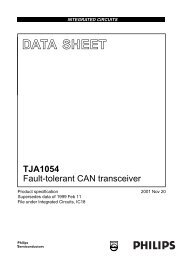
INTEGRATED CIRCUITSDATA SHEET<strong>TJA1053</strong><strong>Fault</strong>-<strong>tolerant</strong> <strong>CAN</strong> <strong>transceiver</strong>Product specificationSupersedes data of 1997 Oct 15File under Integrated Circuits, IC182000 Dec 18
Philips SemiconductorsProduct specification<strong>Fault</strong>-<strong>tolerant</strong> <strong>CAN</strong> <strong>transceiver</strong><strong>TJA1053</strong>FEATURESOptimized for in-car low-speed communication• Baud rate up to 125 kbaud• Up to 32 nodes can be connected• Supports unshielded bus wires• Low RFI due to built-in slope control function• Fully integrated receiver filters• Permanent dominant monitoring of TXD.Bus failure management• Supports one-wire transmission modes with groundoffset voltages up to 1.5 V• Automatic switching to single-wire mode in the event ofbus failure• Automatic reset to differential mode if bus failure isremoved.Protection• Short-circuit proof to battery and ground in 12 Vpowered systems• Thermally protected• Bus lines protected against transients in an automotiveenvironment• An unpowered node does not disturb the bus lines.Support for low-power modes• Low current sleep/standby mode with wake-up via thebus lines• Power-on reset flag on the output.GENERAL DESCRIPTIONThe <strong>TJA1053</strong> is the interface between the <strong>CAN</strong> protocolcontroller and the physical bus. It is primarily intended forlow-speed applications, up to 125 kbaud, in passengercars. The device provides differential transmit capabilitybut will switch in error conditions to a single-wiretransmitter and/or receiver. The <strong>TJA1053</strong> is derived fromthe PCA82C252 giving the following advantages:• Better equipped for networks with more than 15 nodes• Integrated timer at the TXD input prevents a permanentdominant state• Reduced supply current in V CC standby mode• <strong>CAN</strong>H output driver is disabled in the event of a ‘<strong>CAN</strong>Hshort-circuited to battery’ failure mode.QUICK REFERENCE DATASYMBOL PARAMETER CONDITIONS MIN. TYP. MIN. UNITV CC supply voltage 4.75 − 5.25 VV BAT battery voltage no time limit −0.3 − +27 Voperating 6.0 − 27 Vload dump − − 40 VI BAT(sleep) sleep mode current V CC =0V; V BAT =12V − 65 − µAV <strong>CAN</strong>H ,V <strong>CAN</strong>L <strong>CAN</strong>H, <strong>CAN</strong>L input voltage V CC = 0 to 5.5 V; V BAT ≥ 0V; −10 − +27 Vno time limitV CC = 0 to 5.5 V; V BAT ≥ 0V; −40 − +40 Vt < 0.1 ms; load dumpV DROP(H) <strong>CAN</strong>H transmitter drop voltage I <strong>CAN</strong>H =40mA − − 1.4 VV DROP(L) <strong>CAN</strong>L transmitter drop voltage I <strong>CAN</strong>L =40mA − − 1.4 Vt PD propagation delay TXD to RXD − 1 − µst f bus output fall time 90% to 10% − 0.5 − µst r bus output rise time 10% to 90% − 0.5 − µsT amb operating ambient temperature −40 − +125 °C2000 Dec 18 2
Philips SemiconductorsProduct specification<strong>Fault</strong>-<strong>tolerant</strong> <strong>CAN</strong> <strong>transceiver</strong><strong>TJA1053</strong>ORDERING INFORMATIONTYPEPACKAGENUMBER NAME DESCRIPTION VERSION<strong>TJA1053</strong>T SO14 plastic small outline package; 14 leads; body width 3.9 mm SOT108-1BLOCK DIAGRAMhandbook, full pagewidthBATV CC1014INHWAKESTBENTXD17562V CCTIMERWAKE-UPSTANDBYCONTROLTEMPERATUREPROTECTIONDRIVER12.5kΩ911128RTL<strong>CAN</strong>H<strong>CAN</strong>LRTH<strong>TJA1053</strong>NERR4FAILURE DETECTORPLUS WAKE UPPLUS TIME-OUTFILTERRXD3RECEIVERFILTER13MGL181GNDFig.1 Block diagram.2000 Dec 18 3
Philips SemiconductorsProduct specification<strong>Fault</strong>-<strong>tolerant</strong> <strong>CAN</strong> <strong>transceiver</strong><strong>TJA1053</strong>PINNINGSYMBOL PIN DESCRIPTIONINH 1 inhibit output for switching external5 V regulatorTXD 2 transmit data input, when LOW busdata will be dominant, when HIGHbus data will be recessiveRXD 3 receive data output, when LOW busdata will be dominantNERR 4 error output pin, when LOW a buserror existsSTB 5 not standby digital control inputsignal (active LOW)EN 6 enable digital control input signalWAKE 7 not wake input signal, when pulleddown INH becomes active forwake-up (active LOW)RTH 8 termination resistor, <strong>CAN</strong>H line willbe high-impedance with certain buserrorsRTL 9 termination resistor, <strong>CAN</strong>L line will behigh-impedance with certain buserrorsV CC 10 supply voltage (+5 V)<strong>CAN</strong>H 11 high voltage bus line, will be HIGH indominant state<strong>CAN</strong>L 12 low voltage bus line, will be LOW indominant stateGND 13 groundBAT 14 battery voltagehandbook, halfpageINH 114 BATTXD 213RXD 312NERRSTB45<strong>TJA1053</strong>T 1110EN 69WAKE 78MGL182GND<strong>CAN</strong>L<strong>CAN</strong>HV CCRTLRTHFig.2 Pin configuration.2000 Dec 18 4
Philips SemiconductorsProduct specification<strong>Fault</strong>-<strong>tolerant</strong> <strong>CAN</strong> <strong>transceiver</strong><strong>TJA1053</strong>FUNCTIONAL DESCRIPTIONThe <strong>TJA1053</strong> is the interface between the <strong>CAN</strong> protocolcontroller and the physical bus. It is primarily intended forlow speed applications, up to 125 kbaud, in passengercars. The device provides differential transmit capability tothe bus and differential receive capability to the <strong>CAN</strong>controller.To reduce RF interference the rise and fall slope arelimited. This allows the use of an unshielded twisted pair ora parallel pair of wires for the bus. Moreover, it supportstransmission capability on either bus wire if one of the buswires is corrupted. The failure detection logic automaticallyselects a suitable transmission mode.In normal operation (no wiring failures) the differentialreceiver is output to RXD. The differential receiver inputsare connected to <strong>CAN</strong>H and <strong>CAN</strong>L through integratedfilters. The filtered input signals are also used for the singlewire receivers. The <strong>CAN</strong>H and <strong>CAN</strong>L receivers havethreshold voltages that ensure a maximum noise margin insingle-wire modes.A timer has been integrated at the TXD input. This timerprevents the <strong>TJA1053</strong> driving the bus lines to permanentdominant state.Failure detectorThe failure detector is active in the normal operation modeand detects the following single bus failures and switchesto an appropriate mode:1. <strong>CAN</strong>H wire interrupted2. <strong>CAN</strong>L wire interrupted3. <strong>CAN</strong>H short-circuited to battery4. <strong>CAN</strong>L short-circuited to ground5. <strong>CAN</strong>H short-circuited to ground6. <strong>CAN</strong>L short-circuited to battery7. <strong>CAN</strong>L mutually shorted to <strong>CAN</strong>H.The differential receiver threshold is set at −2.9 V.This ensures correct reception in the normal operatingmodes and, in the event of failures 1, 2 and 5 with a noisemargin as high as possible. These failures, or recoveryfrom them, do not destroy ongoing transmissions.Failures 3 and 6 are detected by comparators connectedto <strong>CAN</strong>H and <strong>CAN</strong>L, respectively. If the comparatorthreshold is exceeded for a certain period of time, thereception is switched to the single-wire mode.This time is needed to avoid false triggering by external RFfields. Recovery from these failures is detectedautomatically after a certain time-out (filtering) and notransmission is lost. The <strong>CAN</strong>H driver and the RTH pin areswitched off in the event of failure 3.Failures 4 and 7 initially result in a permanent dominantlevel at RXD. After a time-out, the <strong>CAN</strong>L driver and theRTL pin are switched off. Only a weak pull-up at RTLremains. Reception continues by switching to thesingle-wire mode via <strong>CAN</strong>H. When failures 4 or 7 areremoved, the recessive bus levels are restored. If thedifferential voltage remains below the recessive thresholdlevel for a certain period of time, reception andtransmission switch back to the differential mode.If any of the seven wiring failures occur, the output NERRwill be made LOW. On error recovery, NERR will be madeHIGH again.During all single-wire transmissions, the EMCperformance (both immunity and emission) is worse thanin the differential mode. Integrated receiver filterssuppress any HF noise induced into the bus wires.The cut-off frequency of these filters is a compromisebetween propagation delay and HF suppression. In thesingle-wire mode, low frequency noise cannot bedistinguished from the required signal.Low power modesThe <strong>transceiver</strong> provides 3 low power modes which can beentered and exited via pins STB and EN (see Table 1).The sleep mode is the mode with the lowest powerconsumption. The INH pin is switched to high-impedancefor deactivation of external voltage regulators. <strong>CAN</strong>L isbiased to the battery voltage via the RTL output. If thesupply voltage is provided the RXD and NERR will signalthe wake-up interruptThe V BAT standby mode will react the same as the sleepmode with an active INH output.The V CC standby mode is the V BAT standby with RTLswitched to the V CC voltage. In this mode the NERR outputsignals the V BAT power-on flag and the RXD output willshow the wake-up interrupt.2000 Dec 18 5
Philips SemiconductorsProduct specification<strong>Fault</strong>-<strong>tolerant</strong> <strong>CAN</strong> <strong>transceiver</strong><strong>TJA1053</strong>Wake-up requests are recognized by the <strong>transceiver</strong> whena dominant signal is detected on either bus line or if theWAKE pin is connected to ground. On a wake-up requestthe <strong>transceiver</strong> will set the INH output which can be usedto activate the external V CC voltage regulator. If V CC isprovided the wake-up request can be read on the NERR orRXD outputs, on which the external microcontroller canwake up the <strong>transceiver</strong> (switch to normal operating mode)via STB and EN.To prevent false wake-up due to transients or RF fields,wake-up voltage threshold levels have to be maintainedfor a certain period of time. In the low power modes thefailure detection circuit remains partly active to preventincreased power consumption should errors 3, 4 and 7occur.Power onAfter power-on V BAT is switched on, the INH pin willbecome HIGH and an internal power-on flag will be set.This flag can be read via the NERR pin (STB = 1, EN = 0)and will be reset by entering the normal operation mode.The EN and STB pins will internally be set to LOW level, ifthe V CC voltage is below a certain threshold level, toprovide fail safe functionality.ProtectionsA current limiting circuit protects the transmitter outputstages against short-circuit to positive and negativebattery voltage.If the junction temperature exceeds a maximum value, thetransmitter output stages are disabled. Because thetransmitter is responsible for the major part of the powerdissipation, this will result in a reduced power dissipationand hence a lower chip temperature. All other parts of theIC will remain operating.The <strong>CAN</strong>H and <strong>CAN</strong>L inputs are protected againstelectrical transients which may occur in an automotiveenvironment.Table 1Truth table of <strong>CAN</strong> <strong>transceiver</strong>STB EN MODE INH NERR RXD RTL0 0 V BAT standby (1) HIGH active LOW wake-up interrupt signal if V CC is present switched to V BAT0 0 sleep (2) floating switched to V BAT0 1 go to sleep command floating switched to V BAT1 0 V CC standby (3) HIGH active LOW V BATpower-on flagactive LOW wake-upinterruptswitched to V CC1 1 normal operation mode HIGH active LOW error flag HIGH = receive;LOW = dominantreceived dataswitched to V CCNotes1. Wake-up interrupts are released when entering normal operating mode.2. If go to sleep command was used before (EN may turn LOW as V CC drops, without affecting internal functionsbecause of fail safe functionality).3. V BAT power-on flag will be reset when entering normal operation mode.2000 Dec 18 6
Philips SemiconductorsProduct specification<strong>Fault</strong>-<strong>tolerant</strong> <strong>CAN</strong> <strong>transceiver</strong><strong>TJA1053</strong>LIMITING VALUESIn accordance with the Absolute Maximum Rating System (IEC 60134).V =0to5.5V;SYMBOL PARAMETER CONDITIONS MIN. MAX. UNITV CC supply voltage −0.3 +6.0 VV DD DC input voltage at pins 2 to 6 −0.3 V CC + 0.3 VV BUS DC input voltage at pins 11 and 12 −10 +27 VV <strong>CAN</strong>H , DC input voltage at pins 11 and 12 −40 +40 VV <strong>CAN</strong>LCCV BAT ≥ 0 V; t < 0.1 ms;load dumpV tr transient voltage at pins 11 and 12 see Fig.6 −150 +100 VV WAKE DC input voltage on pin 7 − V BAT + 0.3 VI WAKE input current pin 7 −15 − mAV 1,8,9 DC input voltage on pins 1, 8 and 9 −0.3 V BAT + 0.3 VV BAT DC input voltage on pin 14 −0.3 +27 Vvoltage on pin 14 load dump; 500 ms − 40 VR 8,9 termination resistances pins 8 and 9 500 16000 ΩT vj virtual junction temperature note 1 −40 +150 °CT stg storage temperature −55 +150 °CV esd electrostatic discharge voltage at any pin note 2 −2000 +2000 Vnote 3 −200 +200 VNotes1. Junction temperature in accordance with IEC 60747-1. An alternative definition is: T vj =T amb +PD×R th vj-a .Where: R th vj-a is a fixed value to be used for the calculation of T vj . The rating for T vj limits the allowable combinationsof power dissipation and ambient temperature.2. Human body model: equivalent to discharging a 100 pF capacitor through a 1.5 kΩ resistor.3. Machine model: equivalent to discharging a 200 pF capacitor through a 25 Ω resistor.THERMAL CHARACTERISTICSSYMBOL PARAMETER CONDITIONS VALUE UNITR th vj-a thermal resistance from junction to ambient in free air 120 K/WQUALITY SPECIFICATIONQuality specification in accordance with “SNW-FQ-611-Part-E”.2000 Dec 18 7
Philips SemiconductorsProduct specification<strong>Fault</strong>-<strong>tolerant</strong> <strong>CAN</strong> <strong>transceiver</strong><strong>TJA1053</strong>CHARACTERISTICSV CC = 4.75 to 5.25 V; V STB =V CC ; V BAT = 6 to 27 V; T amb = −40 to +125 °C; all voltages are defined with respect toground; positive currents flow into the IC; all parameters are guaranteed over the temperature range by design, but only100% tested at 25 °C; unless otherwise specified.SYMBOL PARAMETER CONDITIONS MIN. TYP. MAX. UNITSuppliesI CC supply current recessive; TXD = V CC ; − 6 10 mAnormal operating modedominant; TXD = 0 V; no − 29 35 mAload; normal operating modeI CC +I BAT supply current V CC standby; V CC =5V; − 200 500 µAV BAT =12V; T amb
Philips SemiconductorsProduct specification<strong>Fault</strong>-<strong>tolerant</strong> <strong>CAN</strong> <strong>transceiver</strong><strong>TJA1053</strong>SYMBOL PARAMETER CONDITIONS MIN. TYP. MAX. UNITPin INHV dropH HIGH-level voltage drop I INH = −0.18 mA; V BAT 16V − − 1.0 VI LI leakage current sleep mode; V INH =0V −5.0 − +5.0 µAPins <strong>CAN</strong>H and <strong>CAN</strong>LV drxdifferential receiver thresholdvoltageno bus failuresbus failures 1, 2 and 5−3.25 − −2.65 VV o<strong>CAN</strong>Hrec <strong>CAN</strong>H recessive output voltage TXD = V CC ; R RTH
Philips SemiconductorsProduct specification<strong>Fault</strong>-<strong>tolerant</strong> <strong>CAN</strong> <strong>transceiver</strong><strong>TJA1053</strong>SYMBOL PARAMETER CONDITIONS MIN. TYP. MAX. UNITPins RTH and RTLR RTL RTL to V CC switch-on resistance ⎪I o ⎪ < 10 mA;− 7 25 Ωnormal operating mode⎪I o ⎪ < 1 mA; V CC− 15 75 Ωstandby modeRTL to V BAT switch seriesresistanceV BAT standby or sleep mode 8 12.5 23 kΩR RTHRTH to ground switch-onresistance⎪I o ⎪ < 10 mA;normal operating mode− 43 95 ΩV oRTH RTH output voltage I o = 1 mA; low power modes − 0.7 1.0 VI RTLpu RTL pull-up current normal operating mode, − 75 − µAfailures 4, 6 and 7I RTHpd RTH pull-down current normal operating mode, − 75 − µAfailure 3Thermal shutdownT jsd shutdown junction temperature 155 165 180 °CAC CHARACTERISTICSV CC = 4.75 to 5.25 V; V STB =V CC ; V BAT = 6 to 27 V; T amb = −40 to +125 °C; all voltages are defined with respect toground; positive currents flow into the IC; all parameters are guaranteed over the temperature range by design, but only100% tested at 25 °C; unless otherwise specified.SYMBOL PARAMETER CONDITIONS MIN. TYP. MAX. UNITt t(r-d)t t(d-r)t PD(L)<strong>CAN</strong>L and <strong>CAN</strong>H bus outputtransition timerecessive-to-dominant<strong>CAN</strong>L and <strong>CAN</strong>H bus outputtransition timedominant-to-recessivepropagation delay TXD-to-RXDLOW10% to 90%; C1 = 10 nF;C2 = 0; R1 = 100 Ω10% to 90%; C1 = 1 nF;C2 = 0; R1 = 100 ΩC1 = 100 pF; C2 = 0;R1 = 100 Ω; no failures andbus failures 1, 2 and 5C1 = C2 = 3.3 nF;R1 = 100 Ω; no failures andbus failures 1, 2 and 5C1 = 100 pF; C2 = 0;R1 = 100 Ω;bus failures 3, 4, 6 and 7C1 = C2 = 3.3 nF;R1 = 100 Ω;bus failures 3, 4, 6 and 70.6 0.85 − µs0.3 0.4 − µs− 0.75 1.25 µs− 1 1.5 µs− 0.85 1.3 µs− 1.1 1.7 µs2000 Dec 18 10
Philips SemiconductorsProduct specification<strong>Fault</strong>-<strong>tolerant</strong> <strong>CAN</strong> <strong>transceiver</strong><strong>TJA1053</strong>SYMBOL PARAMETER CONDITIONS MIN. TYP. MAX. UNITt PD(H)t wu(min)t WAKE(min)propagation delay TXD-to-RXDHIGHminimum dominant time forwake-up on <strong>CAN</strong>L or <strong>CAN</strong>Hminimum WAKE LOW time forwake-upC1 = 100 pF; C2 = 0;R1 = 100 Ω; no failures andbus failures 1, 2 and 5C1 = C2 = 3.3 nF;R l = 100 Ω; no failures andbus failures 1 and 2C1 = 100 pF; C2 = 0;R1 = 100 Ω;bus failures 3, 4, 6 and 7C1 = C2 = 3.3 nF;R1 = 100 Ω;bus failures 3, 4, 5, 6 and 7low power modesV BAT =12Vlow power modesV BAT =12V− 0.95 1.5 µs− 2.2 3.0 µs− 0.85 1.3 µs− 1.4 2.1 µs8 − 38 µs8 − 38 µst fail failure 3 detection time normal mode 10 − 60 µsfailure 6 detection time normal mode 50 − 400 µsfailure 3 recovery time normal mode 10 − 60 µsfailure 6 recovery time normal mode 150 − 750 µsfailures 4 and 7 detection time normal mode 0.75 − 4.0 msfailures 4 and 7 recovery time normal mode 10 − 60 µsfailures 3, 4 and 7 detection time low power modes;0.8 − 8.0 msV BAT =12Vfailures 3, 4 and 7 recovery time low power modes;V BAT =12V− 4 − mst TXDt h(min)∆ecTXD permanent dominant timer,disable timeminimum hold time to go to sleepcommandnormal mode and failuremodes0.75 − 4.0 ms5 − 50 µsedge-count difference between<strong>CAN</strong>H and <strong>CAN</strong>Lfor failures 1, 2 and 5 detection normal mode − 3 −(NERR becomes LOW)for failures 1, 2 and 5 recovery normal mode − 1 −2000 Dec 18 11
Philips SemiconductorsProduct specification<strong>Fault</strong>-<strong>tolerant</strong> <strong>CAN</strong> <strong>transceiver</strong><strong>TJA1053</strong>TEST AND APPLICATION INFORMATIONndbook, full pagewidth+5 V+12 VINH BAT V CC1 14108RTHR1 (1) C1 (2)WAKE7TXD2STBEN56<strong>TJA1053</strong>1211<strong>CAN</strong>L<strong>CAN</strong>HC2 (2)RXD313 49RTLR1 (1) C1 (2)20 pFGNDNERRMGL183(1) Termination resistors R1 (100 Ω) are not connected to RTH or RTL for testing purposes because the minimum load resistance allowed on the <strong>CAN</strong>bus line is 500 Ω per <strong>transceiver</strong>.(2) The capacitive bus load of 10 nF is split into three equal capacitors (3.3 nF) to simulate the <strong>CAN</strong> bus line.Fig.3 Test circuit for dynamic characteristics.handbook, full pagewidthV TXDV CC0 VV <strong>CAN</strong>LV <strong>CAN</strong>H5 V3.6 V1.4 V0 V2.2 VV diff(1)−2.9 V−5 VV RXDt PD(L) t PD(H)0.7V CC0.3V CCMGL184(1) V diff =V <strong>CAN</strong>H − V <strong>CAN</strong>LFig.4 Timing diagram for dynamic characteristics.2000 Dec 18 12
Philips SemiconductorsProduct specification<strong>Fault</strong>-<strong>tolerant</strong> <strong>CAN</strong> <strong>transceiver</strong><strong>TJA1053</strong>handbook, full pagewidthV BATP8xC592/P8xCE598<strong>CAN</strong> CONTROLLER+5 VBATTERY+5 VCTX0CRXOTXD RXD STB NERR EN INHWAKE723 5 4 6 114BAT<strong>TJA1053</strong><strong>CAN</strong> TRANSCEIVER8 11 12 9RTH <strong>CAN</strong>H <strong>CAN</strong>L RTL1013V CCGND100 nF<strong>CAN</strong> BUS LINEMGL185Fig.5 Application of the <strong>TJA1053</strong>.handbook, full pagewidth+5 V+12 VINH BAT V CC1 14 108RTH100 ΩWAKE7TXD2STBEN56<strong>TJA1053</strong>1211<strong>CAN</strong>L<strong>CAN</strong>H1 nF1 nFGENERATOR20 pFRXD3913 4GND NERRRTL100 ΩMGL186The waveforms of applied transients shall be in accordance with “ISO7637, part 1”, test pulses 1, 2, 3a and 3b.Fig.6 Test circuit for automotive transients.2000 Dec 18 13
Philips SemiconductorsProduct specification<strong>Fault</strong>-<strong>tolerant</strong> <strong>CAN</strong> <strong>transceiver</strong><strong>TJA1053</strong>PACKAGE OUTLINESO14: plastic small outline package; 14 leads; body width 3.9 mmSOT108-1DEAXcyH Ev MAZ148pin 1 indexA 2A 1L pQ(A ) 3θA17Leb pw Mdetail X0 2.5 5 mmscaleDIMENSIONS (inch dimensions are derived from the original mm dimensions)UNITmminchesAmax.1.75A 1 A 2 A 3 b p c D (1) E (1) e H (1)E L L p Q v w y Z0.250.100.069 0.0100.0041.451.250.0570.0490.250.010.490.360.0190.0140.250.190.01000.00758.758.550.350.344.03.80.160.151.270.050Note1. Plastic or metal protrusions of 0.15 mm maximum per side are not included.6.25.80.2440.2281.050.0411.00.40.0390.0160.70.60.0280.0240.250.25 0.10.01 0.01 0.004θ0.70.3 o8o0.028 00.012OUTLINEVERSIONREFERENCESIEC JEDEC EIAJEUROPEANPROJECTIONISSUE DATESOT108-1076E06 MS-01297-05-2299-12-272000 Dec 18 14
Philips SemiconductorsProduct specification<strong>Fault</strong>-<strong>tolerant</strong> <strong>CAN</strong> <strong>transceiver</strong><strong>TJA1053</strong>SOLDERINGIntroduction to soldering surface mount packagesThis text gives a very brief insight to a complex technology.A more in-depth account of soldering ICs can be found inour “Data Handbook IC26; Integrated Circuit Packages”(document order number 9398 652 90011).There is no soldering method that is ideal for all surfacemount IC packages. Wave soldering can still be used forcertain surface mount ICs, but it is not suitable for fine pitchSMDs. In these situations reflow soldering isrecommended.Reflow solderingReflow soldering requires solder paste (a suspension offine solder particles, flux and binding agent) to be appliedto the printed-circuit board by screen printing, stencilling orpressure-syringe dispensing before package placement.Several methods exist for reflowing; for example,convection or convection/infrared heating in a conveyortype oven. Throughput times (preheating, soldering andcooling) vary between 100 and 200 seconds dependingon heating method.Typical reflow peak temperatures range from215 to 250 °C. The top-surface temperature of thepackages should preferable be kept below 220 °C forthick/large packages, and below 235 °C for small/thinpackages.Wave solderingConventional single wave soldering is not recommendedfor surface mount devices (SMDs) or printed-circuit boardswith a high component density, as solder bridging andnon-wetting can present major problems.To overcome these problems the double-wave solderingmethod was specifically developed.If wave soldering is used the following conditions must beobserved for optimal results:• Use a double-wave soldering method comprising aturbulent wave with high upward pressure followed by asmooth laminar wave.• For packages with leads on two sides and a pitch (e):– larger than or equal to 1.27 mm, the footprintlongitudinal axis is preferred to be parallel to thetransport direction of the printed-circuit board;– smaller than 1.27 mm, the footprint longitudinal axismust be parallel to the transport direction of theprinted-circuit board.The footprint must incorporate solder thieves at thedownstream end.• For packages with leads on four sides, the footprint mustbe placed at a 45° angle to the transport direction of theprinted-circuit board. The footprint must incorporatesolder thieves downstream and at the side corners.During placement and before soldering, the package mustbe fixed with a droplet of adhesive. The adhesive can beapplied by screen printing, pin transfer or syringedispensing. The package can be soldered after theadhesive is cured.Typical dwell time is 4 seconds at 250 °C.A mildly-activated flux will eliminate the need for removalof corrosive residues in most applications.Manual solderingFix the component by first soldering twodiagonally-opposite end leads. Use a low voltage (24 V orless) soldering iron applied to the flat part of the lead.Contact time must be limited to 10 seconds at up to300 °C.When using a dedicated tool, all other leads can besoldered in one operation within 2 to 5 seconds between270 and 320 °C.2000 Dec 18 15
Philips SemiconductorsProduct specification<strong>Fault</strong>-<strong>tolerant</strong> <strong>CAN</strong> <strong>transceiver</strong><strong>TJA1053</strong>Suitability of surface mount IC packages for wave and reflow soldering methodsSOLDERING METHODPACKAGEWAVE REFLOW (1)BGA, HBGA, LFBGA, SQFP, TFBGA not suitable suitableHBCC, HLQFP, HSQFP, HSOP, HTQFP, HTSSOP, HVQFN, SMS not suitable (2) suitablePLCC (3) , SO, SOJ suitable suitableLQFP, QFP, TQFP not recommended (3)(4) suitableSSOP, TSSOP, VSO not recommended (5) suitableNotes1. All surface mount (SMD) packages are moisture sensitive. Depending upon the moisture content, the maximumtemperature (with respect to time) and body size of the package, there is a risk that internal or external packagecracks may occur due to vaporization of the moisture in them (the so called popcorn effect). For details, refer to theDrypack information in the “Data Handbook IC26; Integrated Circuit Packages; Section: Packing Methods”.2. These packages are not suitable for wave soldering as a solder joint between the printed-circuit board and heatsink(at bottom version) can not be achieved, and as solder may stick to the heatsink (on top version).3. If wave soldering is considered, then the package must be placed at a 45° angle to the solder wave direction.The package footprint must incorporate solder thieves downstream and at the side corners.4. Wave soldering is only suitable for LQFP, TQFP and QFP packages with a pitch (e) equal to or larger than 0.8 mm;it is definitely not suitable for packages with a pitch (e) equal to or smaller than 0.65 mm.5. Wave soldering is only suitable for SSOP and TSSOP packages with a pitch (e) equal to or larger than 0.65 mm; it isdefinitely not suitable for packages with a pitch (e) equal to or smaller than 0.5 mm.2000 Dec 18 16
Philips SemiconductorsProduct specification<strong>Fault</strong>-<strong>tolerant</strong> <strong>CAN</strong> <strong>transceiver</strong><strong>TJA1053</strong>DATA SHEET STATUSDATA SHEET STATUSPRODUCTSTATUSDEFINITIONS (1)Objective specification Development This data sheet contains the design target or goal specifications forproduct development. Specification may change in any manner withoutnotice.Preliminary specification Qualification This data sheet contains preliminary data, and supplementary data will bepublished at a later date. Philips Semiconductors reserves the right tomake changes at any time without notice in order to improve design andsupply the best possible product.Product specification Production This data sheet contains final specifications. Philips Semiconductorsreserves the right to make changes at any time without notice in order toimprove design and supply the best possible product.Note1. Please consult the most recently issued data sheet before initiating or completing a design.DEFINITIONSShort-form specification ⎯ The data in a short-formspecification is extracted from a full data sheet with thesame type number and title. For detailed information seethe relevant data sheet or data handbook.Limiting values definition ⎯ Limiting values given are inaccordance with the Absolute Maximum Rating System(IEC 60134). Stress above one or more of the limitingvalues may cause permanent damage to the device.These are stress ratings only and operation of the deviceat these or at any other conditions above those given in theCharacteristics sections of the specification is not implied.Exposure to limiting values for extended periods mayaffect device reliability.Application information ⎯ Applications that aredescribed herein for any of these products are forillustrative purposes only. Philips Semiconductors makeno representation or warranty that such applications will besuitable for the specified use without further testing ormodification.DISCLAIMERSLife support applications ⎯ These products are notdesigned for use in life support appliances, devices, orsystems where malfunction of these products canreasonably be expected to result in personal injury. PhilipsSemiconductors customers using or selling these productsfor use in such applications do so at their own risk andagree to fully indemnify Philips Semiconductors for anydamages resulting from such application.Right to make changes ⎯ Philips Semiconductorsreserves the right to make changes, without notice, in theproducts, including circuits, standard cells, and/orsoftware, described or contained herein in order toimprove design and/or performance. PhilipsSemiconductors assumes no responsibility or liability forthe use of any of these products, conveys no licence or titleunder any patent, copyright, or mask work right to theseproducts, and makes no representations or warranties thatthese products are free from patent, copyright, or maskwork right infringement, unless otherwise specified.2000 Dec 18 17
Philips SemiconductorsProduct specification<strong>Fault</strong>-<strong>tolerant</strong> <strong>CAN</strong> <strong>transceiver</strong><strong>TJA1053</strong>NOTES2000 Dec 18 18
Philips SemiconductorsProduct specification<strong>Fault</strong>-<strong>tolerant</strong> <strong>CAN</strong> <strong>transceiver</strong><strong>TJA1053</strong>NOTES2000 Dec 18 19
Philips Semiconductors – a worldwide companyArgentina: see South AmericaAustralia: 3 Figtree Drive, HOMEBUSH, NSW 2140,Tel. +61 2 9704 8141, Fax. +61 2 9704 8139Austria: Computerstr. 6, A-1101 WIEN, P.O. Box 213,Tel. +43 1 60 101 1248, Fax. +43 1 60 101 1210Belarus: Hotel Minsk Business Center, Bld. 3, r. 1211, Volodarski Str. 6,220050 MINSK, Tel. +375 172 20 0733, Fax. +375 172 20 0773Belgium: see The NetherlandsBrazil: see South AmericaBulgaria: Philips Bulgaria Ltd., Energoproject, 15th floor,51 James Bourchier Blvd., 1407 SOFIA,Tel. +359 2 68 9211, Fax. +359 2 68 9102Canada: PHILIPS SEMICONDUCTORS/COMPONENTS,Tel. +1 800 234 7381, Fax. +1 800 943 0087China/Hong Kong: 501 Hong Kong Industrial Technology Centre,72 Tat Chee Avenue, Kowloon Tong, HONG KONG,Tel. +852 2319 7888, Fax. +852 2319 7700Colombia: see South AmericaCzech Republic: see AustriaDenmark: Sydhavnsgade 23, 1780 COPENHAGEN V,Tel. +45 33 29 3333, Fax. +45 33 29 3905Finland: Sinikalliontie 3, FIN-02630 ESPOO,Tel. +358 9 615 800, Fax. +358 9 6158 0920France: 51 Rue Carnot, BP317, 92156 SURESNES Cedex,Tel. +33 1 4099 6161, Fax. +33 1 4099 6427Germany: Hammerbrookstraße 69, D-20097 HAMBURG,Tel. +49 40 2353 60, Fax. +49 40 2353 6300Hungary: see AustriaIndia: Philips INDIA Ltd, Band Box Building, 2nd floor,254-D, Dr. Annie Besant Road, Worli, MUMBAI 400 025,Tel. +91 22 493 8541, Fax. +91 22 493 0966Indonesia: PT Philips Development Corporation, Semiconductors Division,Gedung Philips, Jl. Buncit Raya Kav.99-100, JAKARTA 12510,Tel. +62 21 794 0040 ext. 2501, Fax. +62 21 794 0080Ireland: Newstead, Clonskeagh, DUBLIN 14,Tel. +353 1 7640 000, Fax. +353 1 7640 200Israel: RAPAC Electronics, 7 Kehilat Saloniki St, PO Box 18053,TEL AVIV 61180, Tel. +972 3 645 0444, Fax. +972 3 649 1007Italy: PHILIPS SEMICONDUCTORS, Via Casati, 23 - 20052 MONZA (MI),Tel. +39 039 203 6838, Fax +39 039 203 6800Japan: Philips Bldg 13-37, Kohnan 2-chome, Minato-ku,TOKYO 108-8507, Tel. +81 3 3740 5130, Fax. +81 3 3740 5057Korea: Philips House, 260-199 Itaewon-dong, Yongsan-ku, SEOUL,Tel. +82 2 709 1412, Fax. +82 2 709 1415Malaysia: No. 76 Jalan Universiti, 46200 PETALING JAYA, SELANGOR,Tel. +60 3 750 5214, Fax. +60 3 757 4880Mexico: 5900 Gateway East, Suite 200, EL PASO, TEXAS 79905,Tel. +9-5 800 234 7381, Fax +9-5 800 943 0087Middle East: see ItalyNetherlands: Postbus 90050, 5600 PB EINDHOVEN, Bldg. VB,Tel. +31 40 27 82785, Fax. +31 40 27 88399New Zealand: 2 Wagener Place, C.P.O. Box 1041, AUCKLAND,Tel. +64 9 849 4160, Fax. +64 9 849 7811Norway: Box 1, Manglerud 0612, OSLO,Tel. +47 22 74 8000, Fax. +47 22 74 8341Pakistan: see SingaporePhilippines: Philips Semiconductors Philippines Inc.,106 Valero St. Salcedo Village, P.O. Box 2108 MCC, MAKATI,Metro MANILA, Tel. +63 2 816 6380, Fax. +63 2 817 3474Poland: Al.Jerozolimskie 195 B, 02-222 WARSAW,Tel. +48 22 5710 000, Fax. +48 22 5710 001Portugal: see SpainRomania: see ItalyRussia: Philips Russia, Ul. Usatcheva 35A, 119048 MOSCOW,Tel. +7 095 755 6918, Fax. +7 095 755 6919Singapore: Lorong 1, Toa Payoh, SINGAPORE 319762,Tel. +65 350 2538, Fax. +65 251 6500Slovakia: see AustriaSlovenia: see ItalySouth Africa: S.A. PHILIPS Pty Ltd., 195-215 Main Road Martindale,2092 JOHANNESBURG, P.O. Box 58088 Newville 2114,Tel. +27 11 471 5401, Fax. +27 11 471 5398South America: Al. Vicente Pinzon, 173, 6th floor,04547-130 SÃO PAULO, SP, Brazil,Tel. +55 11 821 2333, Fax. +55 11 821 2382Spain: Balmes 22, 08007 BARCELONA,Tel. +34 93 301 6312, Fax. +34 93 301 4107Sweden: Kottbygatan 7, Akalla, S-16485 STOCKHOLM,Tel. +46 8 5985 2000, Fax. +46 8 5985 2745Switzerland: Allmendstrasse 140, CH-8027 ZÜRICH,Tel. +41 1 488 2741 Fax. +41 1 488 3263Taiwan: Philips Semiconductors, 5F, No. 96, Chien Kuo N. Rd., Sec. 1,TAIPEI, Taiwan Tel. +886 2 2134 2451, Fax. +886 2 2134 2874Thailand: PHILIPS ELECTRONICS (THAILAND) Ltd.,60/14 MOO 11, Bangna Trad Road KM. 3, Bagna, BANGKOK 10260,Tel. +66 2 361 7910, Fax. +66 2 398 3447Turkey: Yukari Dudullu, Org. San. Blg., 2.Cad. Nr. 28 81260 Umraniye,ISTANBUL, Tel. +90 216 522 1500, Fax. +90 216 522 1813Ukraine: PHILIPS UKRAINE, 4 Patrice Lumumba str., Building B, Floor 7,252042 KIEV, Tel. +380 44 264 2776, Fax. +380 44 268 0461United Kingdom: Philips Semiconductors Ltd., 276 Bath Road, Hayes,MIDDLESEX UB3 5BX, Tel. +44 208 730 5000, Fax. +44 208 754 8421United States: 811 East Arques Avenue, SUNNYVALE, CA 94088-3409,Tel. +1 800 234 7381, Fax. +1 800 943 0087Uruguay: see South AmericaVietnam: see SingaporeYugoslavia: PHILIPS, Trg N. Pasica 5/v, 11000 BEOGRAD,Tel. +381 11 3341 299, Fax.+381 11 3342 553For all other countries apply to: Philips Semiconductors,Marketing Communications, Building BE-p, P.O. Box 218, 5600 MD EINDHOVEN,The Netherlands, Fax. +31 40 27 24825Internet: http://www.semiconductors.philips.com© Philips Electronics N.V. 2000 SCA70All rights are reserved. Reproduction in whole or in part is prohibited without the prior written consent of the copyright owner.The information presented in this document does not form part of any quotation or contract, is believed to be accurate and reliable and may be changedwithout notice. No liability will be accepted by the publisher for any consequence of its use. Publication thereof does not convey nor imply any licenseunder patent- or other industrial or intellectual property rights.Printed in The Netherlands 703502/02/pp20 Date of release: 2000 Dec 18 Document order number: 9397 750 07796


