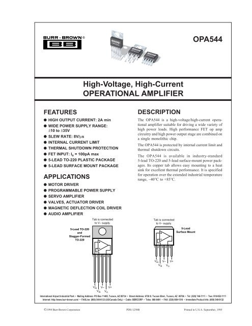
High-Voltage, High-Current OPERATIONAL AMPLIFIER OPA544
High-Voltage, High-Current OPERATIONAL AMPLIFIER OPA544
High-Voltage, High-Current OPERATIONAL AMPLIFIER OPA544

You also want an ePaper? Increase the reach of your titles
YUMPU automatically turns print PDFs into web optimized ePapers that Google loves.
®<strong>OPA544</strong><strong>High</strong>-<strong>Voltage</strong>, <strong>High</strong>-<strong>Current</strong><strong>OPERATIONAL</strong> <strong>AMPLIFIER</strong>FEATURES● HIGH OUTPUT CURRENT: 2A min● WIDE POWER SUPPLY RANGE:±10 to ±35V● SLEW RATE: 8V/µs● INTERNAL CURRENT LIMIT● THERMAL SHUTDOWN PROTECTION● FET INPUT: I B = 100pA max● 5-LEAD TO-220 PLASTIC PACKAGE● 5-LEAD SURFACE MOUNT PACKAGEAPPLICATIONS● MOTOR DRIVER● PROGRAMMABLE POWER SUPPLY● SERVO <strong>AMPLIFIER</strong>● VALVES, ACTUATOR DRIVER● MAGNETIC DEFLECTION COIL DRIVER● AUDIO <strong>AMPLIFIER</strong>5-Lead TO-220andStagger-FormedTO-220Tab is connectedto V– supply.DESCRIPTIONThe <strong>OPA544</strong> is a high-voltage/high-current operationalamplifier suitable for driving a wide variety ofhigh power loads. <strong>High</strong> performance FET op ampcircuitry and high power output stage are combined ona single monolithic chip.The <strong>OPA544</strong> is protected by internal current limit andthermal shutdown circuits.The <strong>OPA544</strong> is available in industry-standard5-lead TO-220 and 5-lead surface-mount power packages.Its copper tab allows easy mounting to a heatsink for excellent thermal performance. It is specifiedfor operation over the extended industrial temperaturerange, –40°C to +85°C.Tab is connectedto V– supply.5-LeadSurface Mount1 2 3 4 51 2 3 4 5+V IN V+–V INV–V O+V IN V+–V INV–V OInternational Airport Industrial Park • Mailing Address: PO Box 11400, Tucson, AZ 85734 • Street Address: 6730 S. Tucson Blvd., Tucson, AZ 85706 • Tel: (520) 746-1111 • Twx: 910-952-1111Internet: http://www.burr-brown.com/ • FAXLine: (800) 548-6133 (US/Canada Only) • Cable: BBRCORP • Telex: 066-6491 • FAX: (520) 889-1510 • Immediate Product Info: (800) 548-6132©1994 Burr-Brown Corporation PDS-1250B Printed in U.S.A. September, 1995
SPECIFICATIONSAt T CASE = +25°C, V S = ±35V, unless otherwise noted.<strong>OPA544</strong>T<strong>OPA544</strong>T-1<strong>OPA544</strong>FPARAMETER CONDITION MIN TYP MAX UNITSOFFSET VOLTAGEInput Offset <strong>Voltage</strong> ±1 ±5 mVvs Temperature Specified Temperature Range ±10 µV/°Cvs Power Supply V S = ±10V to ±35V ±10 ±100 µV/VINPUT BIAS CURRENT (1)Input Bias <strong>Current</strong> V CM = 0V ±15 ±100 pAvs TemperatureSee Typical CurveInput Offset <strong>Current</strong> V CM = 0V ±10 ±100 pANOISEInput <strong>Voltage</strong> NoiseNoise Density, f = 1kHz 36 nV/√Hz<strong>Current</strong> Noise Density, f = 1kHz 3 fA/√HzINPUT VOLTAGE RANGECommon-Mode Input Range, Positive Linear Operation (V+) –6 (V+) –4 VNegative Linear Operation (V–) +6 (V–) +4 VCommon-Mode Rejection V CM = ±V S –6V 90 106 dBINPUT IMPEDANCEDifferential 10 12 || 8 Ω || pFCommon-Mode 10 12 || 10 Ω || pFOPEN-LOOP GAINOpen-Loop <strong>Voltage</strong> Gain V O = ±30V, R L = 1kΩ 90 103 dBFREQUENCY RESPONSEGain Bandwidth Product R L = 15Ω 1.4 MHzSlew Rate 60Vp-p, R L = 15Ω 5 8 V/µsFull-Power BandwidthSee Typical CurveSettling Time 0.1% G = –10, 60V Step 25 µsTotal Harmonic DistortionSee Typical CurveOUTPUT<strong>Voltage</strong> Output, Positive I O = 2A (V+) –5 (V+) –4.4 VNegative I O = 2A (V–) +5 (V–) +3.8 VPositive I O = 0.5A (V+) –4.2 (V+) –3.8 VNegative I O = 0.5A (V–) +4 (V–) +3.1 V<strong>Current</strong> OutputSee SOA CurvesShort-Circuit <strong>Current</strong> 4 APOWER SUPPLYSpecified Operating <strong>Voltage</strong> ±35 VOperating <strong>Voltage</strong> Range ±10 ±35 VQuiescent <strong>Current</strong> I O = 0 ±12 ±15 mATEMPERATURE RANGEOperating –40 +85 °CStorage –40 +125 °CThermal Resistance, θ JC f > 50Hz 2.7 °C/WThermal Resistance, θ JC DC 3 °C/WThermal Resistance, θ JA No Heat Sink 65 °C/WNOTES: (1) <strong>High</strong>-speed test at T J = 25°C.The information provided herein is believed to be reliable; however, BURR-BROWN assumes no responsibility for inaccuracies or omissions. BURR-BROWN assumesno responsibility for the use of this information, and all use of such information shall be entirely at the user’s own risk. Prices and specifications are subject to changewithout notice. No patent rights or licenses to any of the circuits described herein are implied or granted to any third party. BURR-BROWN does not authorize or warrantany BURR-BROWN product for use in life support devices and/or systems.®<strong>OPA544</strong>2
CONNECTION DIAGRAMSTop View5-Lead TO-220andStagger-FormedTO-220Tab is connectedto V– supply.Tab is connectedto V– supply.5-LeadSurface Mount1 2 3 4 5PACKAGE/ORDERING INFORMATIONPACKAGE DRAWINGPRODUCT PACKAGE NUMBER (1)<strong>OPA544</strong>T 5-Lead TO-220 315<strong>OPA544</strong>T-1 5-Lead Stagger-Formed TO-220 323<strong>OPA544</strong>F 5-Lead Surface-Mount 325NOTE: (1) For detailed drawing and dimension table, please see end of datasheet, or Appendix C of Burr-Brown IC Data Book.1 2 3 4 5+V IN V+–V INV–V O+V IN V+–V INV–V OABSOLUTE MAXIMUM RATINGSSupply <strong>Voltage</strong>, V+ to V– ................................................................... 70VOutput <strong>Current</strong> ................................................................. See SOA CurveInput <strong>Voltage</strong> .................................................... (V–) –0.7V to (V+) +0.7VOperating Temperature ................................................. –40°C to +125°CStorage Temperature..................................................... –40°C to +125°CJunction Temperature ...................................................................... 150°CLead Temperature (soldering –10s) (1) ............................................................... 300°CELECTROSTATICDISCHARGE SENSITIVITYThis integrated circuit can be damaged by ESD. Burr-Brownrecommends that all integrated circuits be handled withappropriate precautions. Failure to observe proper handlingand installation procedures can cause damage.ESD damage can range from subtle performance degradationto complete device failure. Precision integrated circuitsmay be more susceptible to damage because very smallparametric changes could cause the device not to meet itspublished specifications.NOTE: (1) Vapor-phase or IR reflow techniques are recommended for solderingthe <strong>OPA544</strong>F surface mount package. Wave soldering is not recommendeddue to excessive thermal shock and “shadowing” of nearby devices.3 <strong>OPA544</strong>®
TYPICAL PERFORMANCE CURVESAt T CASE= +25°C, V S= ±35V, unless otherwise noted.120OPEN-LOOP GAIN AND PHASE vs FREQUENCY10nINPUT BIAS CURRENT vs TEMPERATURE1000Gain (dB)80604020R L = 15Ω–45–90–135–180Phase (°)Input Bias <strong>Current</strong> (A)1n100p10pI BI OS0–201 10 100 1k 10k 100k 1M 10MFrequency (Hz)1p–75 –50 –25 0 25 50 75 100 125Temperature (°C)5CURRENT LIMIT vs TEMPERATURE13QUIESCENT CURRENT vs TEMPERATURELimit <strong>Current</strong> (A)4321Quiescent <strong>Current</strong> (mA)121110V S = ±10VV S = ±35V0–75 –50 –25 0 25 50 75 100 125Temperature (°C)9–75 –50 –25 0 25 50 75 100 125Temperature (°C)100VOLTAGE NOISE DENSITY vs FREQUENCY110COMMON-MODE REJECTION vs FREQUENCY<strong>Voltage</strong> Noise (nV/√Hz)80604020Common-Mode Rejection (dB)1009080706050101 10 100 1k 10k 100kFrequency (Hz)40100 1k 10k 100k 1MFrequency (Hz)®<strong>OPA544</strong>4
TYPICAL PERFORMANCE CURVES (CONT)At T CASE= +25°C, V S= ±35V, unless otherwise noted.120POWER SUPPLY REJECTION vs FREQUENCY2.5GAIN-BANDWIDTH PRODUCT AND SLEW RATEvs TEMPERATUREPower Supply Rejection (dB)100806040V– SupplyV+ SupplyGain-Bandwidth Product (MHz)2.01.51.0GBWSR+SR–987Slew Rate (V/µS)201 10 100 1k 10k 100k 1MFrequency (Hz)0.56–75 –50 –25 0 25 50 75 100 125Temperature (°C)Output <strong>Voltage</strong> (V)353025201510MAXIMUM OUTPUT VOLTAGE vs FREQUENCYClippingSlew RateLimitedTHD + N (%)1010.10.01TOTAL HARMONIC DISTORTION + NOISEvs FREQUENCYR L = 15Ω100mW2W30W5020k 100k 200kFrequency (Hz)0.00120 100 1k 10k 20kFrequency (Hz)5OUTPUT VOLTAGE SWING vs OUTPUT CURRENT6OUTPUT VOLTAGE SWING vs TEMPERATURE|V SUPPLY | – |V OUT | (V)4321(V+) – V O|(V–) –V O ||V SUPPLY | – |V OUT | (V)54321I O = +2AI O = +0.5AI O = –2AI O = –0.5A00 1 2 3Output <strong>Current</strong> (A)0–75 –50 –25 0 25 50 75 100 125Temperature (°C)5 <strong>OPA544</strong>®
TYPICAL PERFORMANCE CURVES (CONT)At T CASE= +25°C, V S= ±35V, unless otherwise noted.SMALL SIGNAL RESPONSEG = 3, C L = 1nF200MV/div5V/divAPPLICATIONS INFORMATIONFigure 1 shows the <strong>OPA544</strong> connected as a basic noninvertingamplifier. The <strong>OPA544</strong> can be used in virtuallyany op amp configuration. Power supply terminals should bebypassed with low series impedance capacitors. The techniqueshown, using a ceramic and tantalum type in parallelis recommended. Power supply wiring should have lowseries impedance and inductance.R 15kΩ+35VV+10µF0.1µF2µs/div+R 210kΩR 2G = 1+ = 3R 1The safe output current decreases as V S –V O increases. Outputshort-circuits are a very demanding case for SOA. A short-circuitto ground forces the full power supply voltage (V+ or V–) acrossthe conducting transistor. With V S = ±35V the safe output currentis 1.5A (at 25˚C). The short-circuit current is approximately 4Awhich exceeds the SOA. This situation will activate the thermalshutdown circuit in the <strong>OPA544</strong>. For further insight on SOA,consult Application Bulletin AB-039.Output <strong>Current</strong> (A)10410.4Output current maybe limited to lessthan 4A—see text.SAFE OPERATING AREA<strong>Current</strong>-LimitedT C = 85°CT C = 25°C<strong>OPA544</strong>V OT C = 125°CV IN0.1µF10µF+Z L0.11 2 5 10|V S – V O | (V)20 50 100FIGURE 2. Safe Operating Area.V––35VFIGURE 1. Basic Circuit Connections.SAFE OPERATING AREAStress on the output transistors is determined by the outputcurrent and the voltage across the conducting output transistor,V S –V O . The power dissipated by the output transistor isequal to the product of the output current and the voltageacross the conducting transistor, V S –V O . The Safe OperatingArea (SOA curve, Figure 2) shows the permissible range ofvoltage and current.CURRENT LIMITThe <strong>OPA544</strong> has an internal current limit set for approximately4A. This current limit decreases with increasingjunction temperature as shown in the typical curve, <strong>Current</strong>Limit vs Temperature. This, in combination with the thermalshutdown circuit, provides protection from many types ofoverload. It may not, however, protect for short-circuit toground, depending on the power supply voltage, ambienttemperature, heat sink and signal conditions.®<strong>OPA544</strong>6
POWER DISSIPATIONPower dissipation depends on power supply, signal and loadconditions. For dc signals, power dissipation is equal to theproduct of output current times the voltage across the conductingoutput transistor. Power dissipation can be minimizedby using the lowest possible power supply voltagenecessary to assure the required output voltage swing.For resistive loads, the maximum power dissipation occursat a dc output voltage of one-half the power supply voltage.Dissipation with ac signals is lower. Application BulletinAB-039 explains how to calculate or measure power dissipationwith unusual signals and loads.HEATSINKINGMost applications require a heat sink to assure that themaximum junction temperature is not exceeded. The heatsink required depends on the power dissipated and onambient conditions. Consult Application Bulletin AB-038for information on determining heat sink requirements.The mounting tab of the surface-mount package versionshould be soldered to a circuit board copper area for goodheat dissipation. Figure 3 shows typical thermal resistancefrom junction to ambient as a function of the copper area.THERMAL PROTECTIONThe <strong>OPA544</strong> has thermal shutdown that protects the amplifierfrom damage. Any tendency to activate the thermalshutdown circuit during normal operation is indication ofexcessive power dissipation or an inadequate heat sink.The thermal protection activates at a junction temperature ofapproximately 155˚C. For reliable operation, junction temperatureshould be limited to 150˚C, maximum. To estimatethe margin of safety in a complete design (including heatsink), increase the ambient temperature until the thermalprotection is activated. Use worst-case load and signal conditions.For good reliability, the thermal protection shouldtrigger more than 25˚C above the maximum expected ambientcondition of your application. This produces a junctiontemperature of 125˚C at the maximum expected ambientcondition.Depending on load and signal conditions, the thermal protectioncircuit may produce a duty-cycle modulated outputsignal. This limits the dissipation in the amplifier, but therapidly varying output waveform may be damaging to someloads. The thermal protection may behave differently dependingon whether internal dissipation is produced bysourcing or sinking output current.OUTPUT STAGE COMPENSATIONThe complex load impedances common in power op ampapplications can cause output stage instability. Figure 3shows an output series R/C compensation network (1Ω inseries with 0.01µF) which generally provides excellent stability.Some variation in circuit values may be required withcertain loads.UNBALANCED POWER SUPPLIESSome applications do not require equal positive and negativeoutput voltage swing. The power supply voltages of the<strong>OPA544</strong> do not need to be equal. For example, a –6Vnegative power supply voltage assures that the inputs of the<strong>OPA544</strong> are operated within their linear common-moderange, and that the output can swing to 0V. The V+ powersupply could range from 15V to 65V. The total voltage (V–to V+) can range from 20V to 70V. With a 65V positivesupply voltage, the device may not be protected from damageduring short-circuits because of the larger V CE duringthis condition.OUTPUT PROTECTIONReactive and EMF-generating loads can return load currentto the amplifier, causing the output voltage to exceed thepower supply voltage. This damaging condition can beavoided with clamp diodes from the output terminal to thepower supplies as shown in Figure 4. Fast-recovery rectifierdiodes with a 4A or greater continuous rating are recommended.50THERMAL RESISTANCE vsCIRCUIT BOARD COPPER AREACircuit Board Copper AreaThermal Resistance, θ JA (°C/W)40302010<strong>OPA544</strong>FSurface Mount Package1oz copper00 1 2 3 4 5Copper Area (inches 2 )<strong>OPA544</strong>Surface Mount PackageFIGURE 3. Thermal Resistance vs Circuit Board Copper Area.7 <strong>OPA544</strong>®
V+R 15kΩR 220kΩRG = – 2= –4R 1V IND 1<strong>OPA544</strong>D 2 1Ω0.01µFMotorV–D 1 , D 2 : Motorola MUR420 Fast Recovery Rectifier.FIGURE 4. Motor Drive Circuit.+30VREF10210V+30V+5V20kΩ8-bitdata port(8 + 4 bits)0-1mA10kΩDAC780112-bitM-DAC20pFOPA60210kΩ4.7kΩ470pF<strong>OPA544</strong>–30V40kΩ10Ω1µH1Ω0.01µFOutput series L/Rnetwork helps assurestability with very highcapacitance loads.V O±20Vat 2AFIGURE 5. Digitally Programmable Power Supply.®<strong>OPA544</strong>8