High-Voltage, High-Current OPERATIONAL AMPLIFIER OPA544
High-Voltage, High-Current OPERATIONAL AMPLIFIER OPA544
High-Voltage, High-Current OPERATIONAL AMPLIFIER OPA544

You also want an ePaper? Increase the reach of your titles
YUMPU automatically turns print PDFs into web optimized ePapers that Google loves.
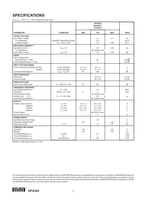
SPECIFICATIONSAt T CASE = +25°C, V S = ±35V, unless otherwise noted.<strong>OPA544</strong>T<strong>OPA544</strong>T-1<strong>OPA544</strong>FPARAMETER CONDITION MIN TYP MAX UNITSOFFSET VOLTAGEInput Offset <strong>Voltage</strong> ±1 ±5 mVvs Temperature Specified Temperature Range ±10 µV/°Cvs Power Supply V S = ±10V to ±35V ±10 ±100 µV/VINPUT BIAS CURRENT (1)Input Bias <strong>Current</strong> V CM = 0V ±15 ±100 pAvs TemperatureSee Typical CurveInput Offset <strong>Current</strong> V CM = 0V ±10 ±100 pANOISEInput <strong>Voltage</strong> NoiseNoise Density, f = 1kHz 36 nV/√Hz<strong>Current</strong> Noise Density, f = 1kHz 3 fA/√HzINPUT VOLTAGE RANGECommon-Mode Input Range, Positive Linear Operation (V+) –6 (V+) –4 VNegative Linear Operation (V–) +6 (V–) +4 VCommon-Mode Rejection V CM = ±V S –6V 90 106 dBINPUT IMPEDANCEDifferential 10 12 || 8 Ω || pFCommon-Mode 10 12 || 10 Ω || pFOPEN-LOOP GAINOpen-Loop <strong>Voltage</strong> Gain V O = ±30V, R L = 1kΩ 90 103 dBFREQUENCY RESPONSEGain Bandwidth Product R L = 15Ω 1.4 MHzSlew Rate 60Vp-p, R L = 15Ω 5 8 V/µsFull-Power BandwidthSee Typical CurveSettling Time 0.1% G = –10, 60V Step 25 µsTotal Harmonic DistortionSee Typical CurveOUTPUT<strong>Voltage</strong> Output, Positive I O = 2A (V+) –5 (V+) –4.4 VNegative I O = 2A (V–) +5 (V–) +3.8 VPositive I O = 0.5A (V+) –4.2 (V+) –3.8 VNegative I O = 0.5A (V–) +4 (V–) +3.1 V<strong>Current</strong> OutputSee SOA CurvesShort-Circuit <strong>Current</strong> 4 APOWER SUPPLYSpecified Operating <strong>Voltage</strong> ±35 VOperating <strong>Voltage</strong> Range ±10 ±35 VQuiescent <strong>Current</strong> I O = 0 ±12 ±15 mATEMPERATURE RANGEOperating –40 +85 °CStorage –40 +125 °CThermal Resistance, θ JC f > 50Hz 2.7 °C/WThermal Resistance, θ JC DC 3 °C/WThermal Resistance, θ JA No Heat Sink 65 °C/WNOTES: (1) <strong>High</strong>-speed test at T J = 25°C.The information provided herein is believed to be reliable; however, BURR-BROWN assumes no responsibility for inaccuracies or omissions. BURR-BROWN assumesno responsibility for the use of this information, and all use of such information shall be entirely at the user’s own risk. Prices and specifications are subject to changewithout notice. No patent rights or licenses to any of the circuits described herein are implied or granted to any third party. BURR-BROWN does not authorize or warrantany BURR-BROWN product for use in life support devices and/or systems.®<strong>OPA544</strong>2