
Create successful ePaper yourself
Turn your PDF publications into a flip-book with our unique Google optimized e-Paper software.
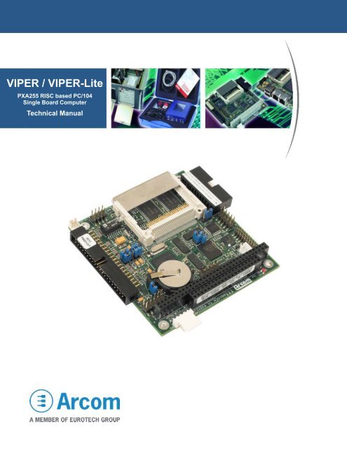
<strong>VIPER</strong> / <strong>VIPER</strong>-LitePXA255 RISC based PC/104Single Board Computer<strong>Technical</strong> <strong>Manual</strong>
<strong>VIPER</strong> <strong>Technical</strong> <strong>Manual</strong>DefinitionsArcom is the trading name for Arcom Control Systems Inc and Arcom Control Systems Ltd.DisclaimerThe information in this manual has been carefully checked and is believed to be accurate. Arcom assumes no responsibilityfor any infringements of patents or other rights of third parties, which may result from its use.Arcom assumes no responsibility for any inaccuracies that may be contained in this document. Arcom makes no commitmentto update or keep current the information contained in this manual.Arcom reserves the right to make improvements to this document and/or product at any time and without notice.WarrantyThis product is supplied with a 3 year limited warranty. The product warranty covers failure of any Arcom manufacturedproduct caused by manufacturing defects. The warranty on all third party manufactured products utilized by Arcom is limitedto 1 year. Arcom will make all reasonable effort to repair the product or replace it with an identical variant. Arcom reserves theright to replace the returned product with an alternative variant or an equivalent fit, form and functional product. Deliverycharges will apply to all returned products. Please check www.arcom.com/support for information about Product Return Forms.TrademarksARM and StrongARM are registered trademarks of ARM Ltd.Intel and XScale are trademarks or registered trademarks of Intel Corporation or its subsidiaries in the United States andother countries.Windows CE is a trademark of the Microsoft Corporation.CompactFlash is the registered trademark of SanDisk Corp.Linux is a registered trademark of Linus Torvalds.RedBoot and Red Hat TM is a registered trademark of Red Hat Inc.VxWorks is a register trademark of Wind River.Bluetooth is a registered trademark of Bluetooth SIG, Inc.All other trademarks recognized.Revision History<strong>Manual</strong> PCB Date CommentsIssue AIssue BV2 Issue 3V2 Issue 4A29 th June 20059 th August 2006First full release of <strong>Manual</strong> for <strong>VIPER</strong> Version 2.Updated to include <strong>VIPER</strong>-Lite details, support for Intel P30Flash, and for full RoHS-6 compliance.Updated to show USB cables with Type A Plugs used to connectto USB Host and Client connectors PL7 and PL17 respectively.Updated to show RS422/485 termination resistor jumpersdisconnected as defaultIssue CV2 Issue 4A25 th January 2007Issue DV2 Issue 4A25 th April 2007© 2007 Arcom.Arcom is a subsidiary of Eurotech Group.www.eurotech.comFor contact details, see page 101.Arcom operates a company-widequality management system,which has been certified by theBritish Standards Institution (BSI)as compliant with ISO9001:2000
<strong>VIPER</strong> <strong>Technical</strong> <strong>Manual</strong>ContentsContentsIntroduction ........................................................................................................................................4<strong>VIPER</strong> ‘at a glance’................................................................................................................5<strong>VIPER</strong>-Lite ‘at a glance’ .........................................................................................................6<strong>VIPER</strong> features ......................................................................................................................7<strong>VIPER</strong> support products ........................................................................................................9Product handling and environmental compliance ................................................................12Conventions .........................................................................................................................13Getting started .................................................................................................................................15Using the <strong>VIPER</strong> ..................................................................................................................15Detailed hardware description .........................................................................................................18<strong>VIPER</strong> block diagram...........................................................................................................18<strong>VIPER</strong> address map ............................................................................................................19Translations made by the MMU ...........................................................................................20PXA255 processor...............................................................................................................21PXA255 GPIO pin assignments...........................................................................................22Real time clock.....................................................................................................................26Watchdog timer....................................................................................................................26Memory ................................................................................................................................27Interrupt assignments ..........................................................................................................30Flat panel display support ....................................................................................................34Audio....................................................................................................................................56General purpose I/O ............................................................................................................57USB host interface ...............................................................................................................60USB client interface .............................................................................................................6110/100BaseTX Ethernet.......................................................................................................62Serial COMs ports................................................................................................................64PC/104 interface ..................................................................................................................67I 2 C.........................................................................................................................................71TPM .....................................................................................................................................71JTAG and debug access......................................................................................................72Power and power management .......................................................................................................73Power supplies.....................................................................................................................73Power management.............................................................................................................74Connectors, LEDs, and jumpers ......................................................................................................85Connectors...........................................................................................................................86Status LEDs .........................................................................................................................97Jumpers ...............................................................................................................................98Appendix A – Contacting Arcom.....................................................................................................101Appendix B – Specification ............................................................................................................102Appendix C – Mechanical diagram ................................................................................................103Appendix D – Reference information .............................................................................................104Appendix E – Acronyms and abbreviations ...................................................................................106Appendix F – RoHS-6 Compliance - Materials Declaration Form..................................................108Index ..............................................................................................................................................109© 2007 Arcom Issue D 3
<strong>VIPER</strong> <strong>Technical</strong> <strong>Manual</strong>IntroductionIntroductionThe <strong>VIPER</strong> is an ultra low power, PC/104 compatible, single board computer availablein two standard variants:• <strong>VIPER</strong>, based on the 400MHz PXA255 XScale processor.• <strong>VIPER</strong>-Lite, based on the 200MHz PXA255 XScale processor.The PXA255 is an implementation of the Intel XScale micro architecture combined witha comprehensive set of integrated peripherals including: a flat panel graphics controller,interrupt controller, real time clock, and multiple serial ports. The <strong>VIPER</strong> board offers awide range of features making it ideal for power sensitive embedded communicationsand multimedia applications.Both of the standard variants are available in two memory configurations, as shownbelow:Variant Memory configuration Details<strong>VIPER</strong> <strong>VIPER</strong>-M64-F32-V2-R6 PXA255 400MHz microprocessor,64MB SDRAM, 32MB FLASH.<strong>VIPER</strong>-M64-F16-V2-R6PXA255 400MHz microprocessor,64MB SDRAM, 16MB FLASH.<strong>VIPER</strong>-Lite <strong>VIPER</strong>L-M64-F32-V2-R6 PXA255 200MHz microprocessor,64MB SDRAM, 32MB FLASH, with reducedfunctionality.<strong>VIPER</strong>L-M64-F16-V2-R6PXA255 200MHz microprocessor,64MB SDRAM, 16MB FLASH, with reducedfunctionality.The <strong>VIPER</strong> and <strong>VIPER</strong>-Lite variants are also available in an industrial temperaturerange. Please contact our Sales team (see Appendix A – Contacting Arcom, page 101)for availability.The following features are not available on the standard <strong>VIPER</strong>-Lite configuration:• PC/104 bus.• USB host controller.• Audio codec.• COM4, COM5 serial ports.• TPM (trusted platform module).• SRAM (static random access memory).Arcom can provide custom configurations (subject to a minimum order quantity) for the<strong>VIPER</strong> or the <strong>VIPER</strong>-Lite. Please contact our Sales team (see Appendix A – ContactingArcom, page 101) to discuss your requirements.© 2007 Arcom Issue D 4
<strong>VIPER</strong> <strong>Technical</strong> <strong>Manual</strong>Introduction<strong>VIPER</strong> ‘at a glance’Five Serial Ports Jumpers 10/100BaseTX EthernetAudio – In/Out/MIC/AMPEthernet LEDsPower(inc reset input)Battery400MHz PXA255processor8/16-bit PC/104interfaceJTAGTPM Tamper(Optional)Intel StrataFLASHJumpersUSB ClientDigital I/OUSBTFT/STN panelCompactFLASH (CF+)© 2007 Arcom Issue D 5
<strong>VIPER</strong> <strong>Technical</strong> <strong>Manual</strong>Introduction<strong>VIPER</strong>-Lite ‘at a glance’Three Serial Ports10/100BaseTX EthernetEthernet LEDsPower(inc reset input)Battery200MHz PXA255processorJTAGIntel StrataFLASHJumpersUSB ClientDigital I/OTFT/STN panelCompactFLASH (CF+)© 2007 Arcom Issue D 6
<strong>VIPER</strong> <strong>Technical</strong> <strong>Manual</strong>Introduction<strong>VIPER</strong> featuresMicroprocessorCacheSystem memorySilicon diskVideoAudioVLVLVL• PXA255 400MHz (<strong>VIPER</strong>) or 200MHz (<strong>VIPER</strong>-Lite) RISC processor.• 32K data cache, 32K instruction cache, 2K mini data cache.• 64MB un-buffered 3.3V SDRAM.• Up to 16/32MB Intel StrataFLASH (with FLASH access LED).• 1MB bootloader FLASH EPROM (with FLASH access LED).• 256KB SRAM (battery backed).• Type I/II CompactFLASH (CF+) socket.• TFT/STN (3.3V or 5V) flat panel graphics controller.• Up to 640X480 resolution.• 8/16bpp.• Backlight control.• National Semiconductor LM4529 AC’97 CODEC and LM4880 power amp.• Line IN, line OUT, microphone, and 250mW per channel amplified output.Serial ports 1• 5 x 16550 compatible high-speed UARTs.• 4 x RS232 and 1 x RS422/485 Interfaces.• 2 x channels with 128Byte Tx/Rx FIFO.USB host interfaceVLUSB client interface• Two USB 1.1 compliant interfaces.• Short circuit protection and 500mA current limit protection.• One USB 1.1 client interface.1 COM4 (RS232) and COM5 (RS422/485) are not available on the <strong>VIPER</strong>-Lite.© 2007 Arcom Issue D 7
<strong>VIPER</strong> <strong>Technical</strong> <strong>Manual</strong>IntroductionNetwork support• SMSC LAN91C111 10/100BaseTX Ethernet controller.• One 10/100BaseTX NIC port.Trusted Platform Module (TPM) [optional]VLVL• Atmel AT97SC3201 TPM security, with full TCG/TCPA V1.1b compatibility.• Includes crypto accelerator capable of computing a 1024-bit RSA signaturein 100ms.Real time clock (RTC)Watchdog• Battery backed RTC.• ± 1minute/month accuracy, at 25°C.• Adjustable timeout of 271ns to 19 minutes 25 seconds.General purpose I/O (GPIO)• 8 x 3.3V tolerant inputs (5V tolerant).• 8 x 3.3V outputs.User configuration• 1 user-configurable jumper.ExpansionJTAG portPowerBattery backupSizeEnvironmentalVL• PC/104 expansion bus - 8/16-bit ISA bus compatible interface.• Download data to FLASH memory.• Debug and connection to In-Circuit Emulator (ICE).• Typically 2W from a single 5V supply.• Power management features allowing current requirements to be as low as49mA (245mW).• Onboard battery holder containing a lithium-ion non-rechargeable CR2032,3V, 220mAh battery.• PC/104 compatible footprint 3.8” x 3.6” (96mm x 91mm).• Operating temperature range:- Commercial: -20 o C (-4 o F) to +70 o C (+158 o F)- Industrial: -40 o C (-40 o F) to +85 o C (+185 o F)• RoHS directive (2002/95/EC) compliant© 2007 Arcom Issue D 8
<strong>VIPER</strong> <strong>Technical</strong> <strong>Manual</strong>Introduction<strong>VIPER</strong> support productsThe <strong>VIPER</strong> supports the following products:• <strong>VIPER</strong>-UPS (Uninterruptible Power Supply)The <strong>VIPER</strong>-UPS serves as a 5V DC power supply and battery back up system forthe <strong>VIPER</strong>. The UPS accepts between 10 – 36 VDC (10-25VAC) input andgenerates the +5V supply for the <strong>VIPER</strong>. In addition to this, it includes an intelligentbattery charger/switch capable of using either the onboard 500mAHr NiMH batteryor an external sealed lead acid rechargeable battery. For further details, seewww.arcom.com/products/icp/pc104/processors/viper_UPS.htm.• <strong>VIPER</strong>-FPIF1 (Flat Panel Interface)The <strong>VIPER</strong>-FPIF1 is a simple board that enables easy connection between the<strong>VIPER</strong> and an LCD flat panel. See the section <strong>VIPER</strong>-FPIF1 details, page 38, forfurther details. Contact Arcom (see Appendix A – Contacting Arcom, page 101) forpurchasing information.• ETHER-BREAKOUTThe ETHER-BREAKOUT is a simple board that converts the <strong>VIPER</strong> Ethernet 8-pinheader and Ethernet LEDs 6-pin header to a standard RJ45 connector with LEDs.Contact Arcom (see Appendix A – Contacting Arcom, page 101) for purchasinginformation.• FPIF-LVDS-TX (Flat Panel Interface)The FPIF-LVDS-TX enables LVDS displays to be connected to the <strong>VIPER</strong>. TheFPIF-LVDS-TX in combination with the FPIF-LVDS-RX allows the <strong>VIPER</strong> to drive aTFT or STN LCD flat panel display up to 10 meters away. See the section FPIF-LVDS-TX details, page 43, for further details. Contact Arcom (see Appendix A –Contacting Arcom, page 101) for purchasing information.• FPIF-LVDS-RX (Flat Panel Interface)The FPIF-LVDS-RX in combination with the FPIF-LVDS-TX allows the <strong>VIPER</strong> todrive a TFT or STN LCD flat panel display up to 10 meters away. See the sectionFPIF-LVDS-RX details, page 48, for further details. Contact Arcom (see Appendix A– Contacting Arcom, page 101) for purchasing information.• FPIF-CRT (CRT Monitor or Analog FPD Interface)The FPIF-CRT is a simple board that enables easy connection between the <strong>VIPER</strong>and a CRT Monitor or analog LCD flat panel. See the section FPIF-CRT details,page 53, for further details. Contact Arcom (see Appendix A – Contacting Arcom,page 101) for purchasing information.• <strong>VIPER</strong>-I/O<strong>VIPER</strong>-I/O is a low cost add-on I/O module for the PXA255 <strong>VIPER</strong> board. The boardprovides a variety of I/O features without the additional costs of a full PC/104interface. The combination of the <strong>VIPER</strong> and <strong>VIPER</strong>–I/O is suited to control andmonitoring applications that require a limited number of isolated inputs and outputs.See the section <strong>VIPER</strong>-I/O, page 59, for further details. Contact Arcom (seeAppendix A – Contacting Arcom, page 101) for purchasing information.© 2007 Arcom Issue D 9
<strong>VIPER</strong> <strong>Technical</strong> <strong>Manual</strong>Introduction• CYCLOPSThe CYCLOPS is a rugged <strong>VIPER</strong> display terminal. The enclosure can beconfigured to suit a complete range of embedded applications with LCD display andtouchscreen.• <strong>VIPER</strong>-ICE (Industrial Compact Enclosure) development kitsThe <strong>VIPER</strong>-ICE is a simple low cost aluminum enclosure, which provides easyconnection to all on board features. The enclosure includes the <strong>VIPER</strong>-UPS andoptionally a color Q-VGA (320x240) TFT flat panel display and analog touchscreen.The <strong>VIPER</strong>-ICE is available with a wide range of development kits. These aredescribed in the section Development kits available for the <strong>VIPER</strong>, page 10. Forfurther details, see www.arcom.com/development-kits.htm.Development kits available for the <strong>VIPER</strong>• Windows CE/CE 5.0 development kitFeatures of this kit are:- 400MHz PXA255 processor with 64MB DRAM & 32MB Flash memory.- Pre-configured build of Windows CE 5.0 tailored specifically for the <strong>VIPER</strong>, preloadedinto the 32MB Flash.- Windows CE 5.0 Platform SDK for <strong>VIPER</strong>.- Rugged enclosure with NEC Q-VGA TFT color 5.5 and display and analogtouchscreen.- Uninterruptible power supply (<strong>VIPER</strong>-UPS) to allow <strong>VIPER</strong> system to continue tooperate without main power. Example code is supplied to handle the power losswarning and battery backup control features.- 24V power supply module with power cords for US, UK, and European powersockets.- Arcom Development Kit CD containing Windows CE 5.0 operating system image,sample code, <strong>Technical</strong> <strong>Manual</strong>, and datasheets.- Quickstart manual.• Embedded Linux development kitFeatures of this kit are:- 400MHz PXA255 processor with 64MB DRAM & 32MB Flash memory.- Pre-configured build of Arcom’s Embedded Linux, tailored specifically for the<strong>VIPER</strong>, pre-loaded into the 32MB Flash.- 2.6-based Linux kernel release, GNU C library.- Compressed Journaling Flash File System (JFFS2) offering high reliability andrecovery from power interruptions.- Rugged enclosure with optional NEC Q-VGA TFT color display and analogtouchscreen.- Uninterruptible power supply (<strong>VIPER</strong>-UPS) to allow <strong>VIPER</strong> system to continue tooperate without main power.- 24V power supply module with power cords for US, UK, and European powersockets.- Optional - high performance IBM J9 VM.- Quickstart tutorial guide.© 2007 Arcom Issue D 10
<strong>VIPER</strong> <strong>Technical</strong> <strong>Manual</strong>Introduction• Wind River VxWorks 5.5 development kitFeatures of this kit are:- 400MHz PXA255 processor with 64MB DRAM & 32MB Flash memory.- VxWorks BSP for Tornado 2.2.1/VxWorks 5.5.1/Wind ML 3.0.2.- Pre-configured build of VxWorks, tailored specifically for the <strong>VIPER</strong>, pre-loadedinto the 32MB Flash.- Rugged enclosure with optional NEC Q-VGA TFT color display and analogtouchscreen.- Uninterruptible power supply (<strong>VIPER</strong>-UPS) to allow <strong>VIPER</strong> system to continue tooperate without main power.- 24V power supply module with power cords for US, UK, and European powersockets.Entry level development kits for <strong>VIPER</strong> or <strong>VIPER</strong>-LiteThe following entry level development kits are available:• Windows CE / CE 5.0 development kitFeatures of this kit for <strong>VIPER</strong> or <strong>VIPER</strong>-Lite are:- 400MHz (<strong>VIPER</strong>) or 200MHz (<strong>VIPER</strong>-Lite) PXA255 processor with 64MB DRAM& 32MB Flash memory.- Pre-configured build of Windows CE 5.0 tailored specifically for the <strong>VIPER</strong>, preloadedinto the 32MB Flash.- +5V PSU.- All cables for immediate operation and download.- Development kit documentation.- Optional <strong>VIPER</strong>-I/O module.• Embedded Linux development kitFeatures of this kit for <strong>VIPER</strong> or <strong>VIPER</strong>-Lite are:- 400MHz (<strong>VIPER</strong>) or 200MHz (<strong>VIPER</strong>-Lite) PXA255 processor with 64MB DRAM& 32MB Flash memory.- Pre-configured build of Arcom’s Embedded Linux, tailored specifically for the<strong>VIPER</strong>, pre-loaded into the 32MB Flash.- +5V PSU.- All cables for immediate operation and download.- Development kit documentation.- Optional <strong>VIPER</strong>-I/O module.© 2007 Arcom Issue D 11
<strong>VIPER</strong> <strong>Technical</strong> <strong>Manual</strong>IntroductionProduct handling and environmental complianceAnti-static handlingThis board contains CMOS devices that could be damaged in the event of staticelectricity discharged through them. At all times, please observe anti-static precautionswhen handling the board. This includes storing the board in appropriate anti-staticpackaging and wearing a wrist strap when handling the board.PackagingPlease ensure that should a board need to be returned to Arcom, it is adequatelypacked, preferably in the original packing material.Electromagnetic compatibility (EMC)The <strong>VIPER</strong> is classified as a component with regard to the European Community EMCregulations and it is the users responsibility to ensure that systems using the board arecompliant with the appropriate EMC standards.RoHS ComplianceThe European RoHS Directive (Restriction on the use of certain HazardousSubstances – Directive 2002/95/EC) limits the amount of 6 specific substances withinthe composition of the product. The <strong>VIPER</strong>, <strong>VIPER</strong>-Lite, and associated accessoryproducts are available as RoHS-6 compliant options and are identified by a -R6 suffix inthe product order code. A full RoHS Compliance Materials Declaration Form is includedin Appendix F – RoHS-6 Compliance - Materials Declaration Form, page 108. Furtherinformation about RoHS compliance is available on the Arcom web site –http://www.arcom.com/RoHS_and_WEEE/.© 2007 Arcom Issue D 12
<strong>VIPER</strong> <strong>Technical</strong> <strong>Manual</strong>IntroductionConventionsSymbolsThe following symbols are used in this guide:SymbolExplanationNote - information that requires your attention.Tip - a handy hint that may provide a useful alternative or save time.Caution - proceeding with a course of action may damage your equipmentor result in loss of data.VLIndicates that a feature is not available on the standard <strong>VIPER</strong>-Liteconfiguration. Arcom can provide custom configurations (subject to aminimum order quantity) for the <strong>VIPER</strong>-Lite populated with this feature.Please contact our Sales team (see Appendix A – Contacting Arcom, page101) to discuss your requirements.Jumper is fitted.Jumper is not fitted.321321Jumper fitted on pins 1-2.Jumper fitted on pins 2-3.© 2007 Arcom Issue D 13
<strong>VIPER</strong> <strong>Technical</strong> <strong>Manual</strong>IntroductionTablesWith tables such as that shown below, the white cells show information relevant to thesubject being discussed. Grey cells are not relevant in the current context.Byte lane Most Significant Byte Least Significant ByteBit 15 14 13 12 11 10 9 8 7 6 5 4 3 2 1 0Field - - - - - - - - - - - - - RETRIG AUTO_CLRReset X X X X X X X X 0 0 0 0 0 0 0 0R_DISRelevantinformation© 2007 Arcom Issue D 14
<strong>VIPER</strong> <strong>Technical</strong> <strong>Manual</strong>Getting startedGetting startedUsing the <strong>VIPER</strong>Depending on the development kit purchased, a Quickstart <strong>Manual</strong> is provided forWindows CE, embedded Linux, or VxWorks to enable users to set-up and start usingthe board. Please read the relevant manual and follow the steps defining the set-up ofthe board. Once you have completed this task you will have a working <strong>VIPER</strong> systemand can start adding further peripherals enabling development to begin.This section provides a guide to setting up and using of some of the features of the<strong>VIPER</strong>. For more detailed information on any aspect of the board see Detailedhardware description, page 18.Using the CompactFLASH socketThe <strong>VIPER</strong> is fitted with a Type I/II CompactFLASH socket mounted on the topside ofthe board. The socket is connected to Slot 0 of the PXA255 PC card interface. Itsupports 3.3V Type I and II CompactFLASH cards for both memory and IO. The <strong>VIPER</strong>supports hot swap changeover of the cards and notification of card insertion.RedBoot supports ATA type CompactFlash cards. Files can be read providing the cardis formatted with an EXT2 file system. Eboot cannot boot from CompactFlash.5V CompactFLASH is not supported.The CompactFLASH card can only be inserted one way into the socket. Thecorrect orientation is for the top of the card, i.e. with the normal printed side facedown to the PCB.Using the serial interfaces (RS232/422/485)The five serial port interfaces on the <strong>VIPER</strong> are fully 16550 compatible. Connection tothe serial ports is made via a 40-way boxed header. The pin assignment of this headerhas been arranged to enable 9-way IDC D-Sub plugs to be connected directly to thecable. See the section PL4 – COMS ports, page 89, for pin assignment and connectordetails.A suitable cable for COM1 is provided as part of the development kit. The D-Subconnector on this cable is compatible with the standard 9-way connector on a desktopcomputer.VLCOM4 (RS232) and COM5 (RS422/485) are not available on the standard<strong>VIPER</strong>-Lite configuration. Arcom can provide custom configurations (subject to aminimum order quantity) for the <strong>VIPER</strong>-Lite populated with this feature. Pleasecontact our Sales team (see Appendix A – Contacting Arcom, page 101) todiscuss your requirements.© 2007 Arcom Issue D 15
<strong>VIPER</strong> <strong>Technical</strong> <strong>Manual</strong>Getting startedUsing the audio featuresVLThere are four audio interfaces supported on the <strong>VIPER</strong>: amp out, line out, line in, andmicrophone. The line in, line out, and amp interfaces support stereo signals and themicrophone provides a mono input. The amplified output is suitable for driving an 8Ωload with a maximum power output of 250mW per channel. Connections are routed toPL6 - see the sections Audio (page 56) and PL6 – Audio connector (page 91) for furtherdetails.Using the USB hostThe standard USB connector is a 4-way socket, which provides power and data signalsVL to the USB peripheral. The 10-way header PL7 has been designed to be compatiblewith PC expansion brackets that support two USB sockets. See the sections USB hostinterface (page 60) and PL7 – USB connector (page 91) for further details.Using the USB clientThe <strong>VIPER</strong> board can be used as USB client and connected to a PC via a USB cable.The USB cable should be plugged into PL17 header. See the sections USB clientinterface (page 61) and PL17 – USB client connector (page 95) for further details.Using the Ethernet interfaceThe SMSC LAN91C111 10/100BaseTX Ethernet controller is configured by theRedBoot bootloader for embedded Linux or VxWorks, and by Eboot for Windows CE.Connection is made via connector PL1. A second connector PL2 provides activity andlink status outputs for control LEDs. See the sections 10/100BaseTX Ethernet (page62), PL1 – 10/100BaseTX Ethernet connector (page 87) and PL2 – Ethernet statusLEDs connector (page 87) for further details.The Ethernet port may be connected to an ETHER-BREAKOUT module to provide astandard RJ45 port connector, see section Ethernet breakout board, page 62 for furtherdetails.© 2007 Arcom Issue D 16
<strong>VIPER</strong> <strong>Technical</strong> <strong>Manual</strong>Getting startedUsing the PC/104 expansion busVLPC/104 modules can be used with the <strong>VIPER</strong> to add extra functionality to the system.This interface supports 8/16 bit ISA bus style peripherals.Arcom has a wide range of PC/104 modules, which are compatible with the <strong>VIPER</strong>.These include modules for digital I/O, analog I/O, motion control, CAN bus, serialinterfaces, etc. Please contact the Arcom sales team if a particular interface you requiredoes not appear to be available as these modules are in continuous development.Contact details are provided in Appendix A – Contacting Arcom, page 101.In order to use a PC/104 board with the <strong>VIPER</strong> it should be plugged into PL11 for 8-bitcards and PL11/PL12 for 8/16-bit cards. See the sections PC/104 interface (page 67)and PL11 & PL12 – PC/104 connectors (page 94) for further details.The ISA interface on the <strong>VIPER</strong> does not support DMA or shared interrupts. See thesection Interrupt assignments, page 30, for details about PC/104 interrupt use.The <strong>VIPER</strong> provides +5V to a PC/104 add-on board via the PL11 and PL12 connectors.If a PC/104 add-on board requires a +12V supply, then +12V must be supplied to the<strong>VIPER</strong> power connector PL16 pin 4. If –12V or –5V are required, these must besupplied directly to the PC/104 add-on board.The <strong>VIPER</strong> is available with non-stack through connectors by special order. ContactArcom (see Appendix A – Contacting Arcom, page 101, for more details.© 2007 Arcom Issue D 17
<strong>VIPER</strong> <strong>Technical</strong> <strong>Manual</strong>Detailed hardware descriptionDetailed hardware description<strong>VIPER</strong> block diagramThe following section provides a detailed description of the functions provided by the<strong>VIPER</strong>. This information may be required during development after you have startedadding extra peripherals or are starting to use some of the embedded features.The diagram below illustrates the functional organization of the <strong>VIPER</strong> PC/104 SBC.Functions that are not available with the standard <strong>VIPER</strong>-Lite are highlighted in orange.<strong>VIPER</strong>PL4PL1&PL2PL17PL7PL8COM 1COM 2&3COM 4COM5JP110/100baseTX5VI 2 CTPMRS232TransceiversRS422/485TransceiverTransformerUSB ClientUSB PowerSwitchUSB1 & 2OptionalSerialEEPROM3VBackupGPIO[26:27]DUARTLAN91C11164MBSDRAM1MBBootloaderFLASH16 or 32MBSiliconDiskUSB HostController3VBackup256kBSRAMControlControlAddress & DataControlPXA25514.318MHzAC'97SignalsBLKEN &LCDENPWM13.6864MHz3VBackup3.3VClockGenerationRTCPowerAmpAC'97CodecLCD SignalsJP2DualMOSFETReg1.8432MHz6MHz8MHz14.318MHz24.576MHz25MHz33MHzAMP R+L32.768kHzLINE IN R+LLINE OUT R+LMIC IN5VLCD_SupplyJumper ConfigurationBLKSAFE &LCDSAFELCDENPOSBIAS /NEGBIASPL6PL3JP3PL9PL11&PL12PL55VIN[0:7] / OUT[0:7]PC/104 Address & DataPC/104 ControlPC/104 InterruptsCF Address & DataCF Control3.3VTransceiversTransceiversCPLDTransceiversCF PowerSwitchControlCF & PC/104 Control SignalsCF_SWITCHCR20323VBackup3.3V1.06-1.29V3.3VControl1.8VJTAGVoltageMonitorTriple RegMicropowerDACRegJP4INT_VBAT_INEXT_VBAT_IN5VPL10PL16© 2007 Arcom Issue D 18
<strong>VIPER</strong> <strong>Technical</strong> <strong>Manual</strong>Detailed hardware description<strong>VIPER</strong> address mapVLVLVLVLVLVLVLVLVLPXA255chipselectPhysical addressBus/registerwidthDescription- 0xA4000000 – 0xFFFFFFFF - ReservedSDCS0 0xA0000000 – 0xA3FFFFFC 32-bit SDRAM, IC2&3- 0x4C000000 – 0x9FFFFFFF - ReservedNA 0x48000000 – 0x4BFFFFFF 32-bit Memory Control Registers 1NA 0x44000000 – 0x47FFFFFF 32-bit LCD Control Registers 1NA 0x40000000 – 0x43FFFFFF 32-bit PXA255 Peripherals 1- 0x3C200400 – 0x3FFFFFFF - ReservedNA 0x3C000000 – 0x3C1FFFFF 8/16-bit PC/104 Memory Space- 0x30000400 – 0x3BFFFFFF - ReservedNA 0x30000000 – 0x300003FF 8/16-bit PC/104 I/O SpaceNA 0x20000000 – 0x2FFFFFFF 32-bit CompactFLASH, PL5- 0x14880000 – 0x1FFFFFFF - ReservedCS5 0x14800000 – 0x1487FFFF 16-bit SRAM (see page 28)- 0x14500002 – 0x47FFFFFF - ReservedCS5 0x14500000 – 0x14500001 16-bit General purpose I/O (see page57)- 0x14300020 – 0x144FFFFF - ReservedCS5 0x14300010 – 0x1430001F 16-bit COM4 (see page 65)CS5 0x14300000 – 0x1430000F 16-bit COM5 (see page 65)- 0x14100006 – 0x142FFFFF - ReservedCS5 0x14100004 – 0x14100005 16-bit PC104I2 Register (see page 31)CS5 0x14100002 – 0x14100003 16-bit ICR Register (see page 31)CS5 0x14100000 – 0x14100001 16-bit PC104I1 Register (see page 31)- 0x10000004 – 0x140FFFFF - ReservedCS4 0x10000000 – 0x100007FF 32-bit Ethernet Data port- 0x0C000004 – 0x0FFFFFFF - ReservedCS3 0x0C000000 – 0x0C000002 16-bit USB Host Controller- 0x08000310 – 0x0BFFFFFF - ReservedCS2 0x08000300 – 0x0800030E 16-bit Ethernet I/O Space- 0x06000000 – 0x080002FF - ReservedCS1 0x04000000 – 0x05FFFFFE 16-bit FLASH Memory / Silicon Disk- 0x00100000 – 0x03FFFFFF - ReservedCS0 0x00000000 – 0x000FFFFE 16-bit Bootloader FLASH1Details of the internal registers are in the Intel Developer <strong>Manual</strong> on the Development Kit CD.© 2007 Arcom Issue D 19
<strong>VIPER</strong> <strong>Technical</strong> <strong>Manual</strong>Detailed hardware descriptionTranslations made by the MMUFor details of translations made by the MMU by Redboot for embedded Linux, pleaserefer to the <strong>VIPER</strong> Embedded Linux AEL <strong>Technical</strong> <strong>Manual</strong>.For details of translations made by the MMU by Redboot for VxWorks, please refer tothe <strong>VIPER</strong> VxWorks Quickstart and <strong>Technical</strong> <strong>Manual</strong>.For details of translations made by the MMU for Windows CE, please check theWindows CE documentation for more information about memory mapping. One sourceof this information is on the MSDN web site (www.msdn.microsoft.com) under WindowsCE Memory Architecture.© 2007 Arcom Issue D 20
<strong>VIPER</strong> <strong>Technical</strong> <strong>Manual</strong>Detailed hardware descriptionPXA255 processorThe PXA255 is a low power ARM (version 5TE) instruction set compliant RISCprocessor. The PXA255 does not include a floating-point unit. The device does,however, contain a DSP co-processor to enhance multimedia applications.The <strong>VIPER</strong> is fitted with a 400MHz PXA255 variant and the <strong>VIPER</strong>-Lite is fitted with a200MHz PXA255 variant. The clock source for these is a 3.6864 MHz clock, whichgenerates all the high-speed clocks within the device. The default run mode frequencyis 400MHz for the <strong>VIPER</strong> and 200MHz for the <strong>VIPER</strong>-Lite. Currently embedded Linuxand VxWorks supports changing the operating frequency and Windows CE will providesupport shortly. Please refer to the relevant operating system technical manual to selectan alternative operating frequency.The processor has two supply inputs: I/O and core generated on the <strong>VIPER</strong> from themain +5V supply input. The I/O supply is powered from +3.3V, and the core is poweredfrom a +1.06 to +1.3V adjustable supply. See the section Processor powermanagement, page 81, for operation details.The PXA255 has an integrated memory and CompactFlash controller with 100 MHzmemory bus, 32KB data and 32KB instruction caches, and 2KB mini data cache forstreaming data.The PXA255 provides up to 85 GPIO pins, many of which have been configured foralternative functions like the AC’97 and PC card/CompactFLASH interfaces. Details ofthese pin configurations are provided in the section PXA255 GPIO pin assignments,page 22.The PXA255 also has the following features that can be used on the <strong>VIPER</strong>:• Peripheral Control Module:- 16 channel configurable DMA controller (for internal use only).- Integrated LCD controller with unique DMA for fast color screen support.- Serial ports including AC’97, 3 UARTs, and enhanced USB end point interface.• System Control Module:- General-purpose interruptible I/O ports.- Real time clock.- Watchdog.- Interval timers.- Power management controller.- Interrupt controller.- Reset controller.- Two on-chip oscillators.The PXA255 processor is packaged in a 256-pin PBGA, which is attached to the boardduring the assembly process.The PXA255 processor is a low power device and does not require a heat sink fortemperatures up to 70°C (85°C for the industrial variant).© 2007 Arcom Issue D 21
<strong>VIPER</strong> <strong>Technical</strong> <strong>Manual</strong>Detailed hardware descriptionPXA255 GPIO pin assignmentsThe following table summarizes the use of the 85 PXA255 GPIO pins, their direction,alternate function, and active level.For embedded Linux the GPIO pins are setup by Redboot. Under VxWorks andWindows CE, they are setup by the OS and not by the bootloader.Key:AFDirActiveSleepAlternate function.Pin direction.Function active level or edge.Pin state during sleep mode (all Hi-Z states are to ‘1’ during sleep).GPIONo AF Signal name Dir Active Sleep Function See section…0 0 ETHER_INT Input Input Ethernet InterruptVLVLVL1 0 PC/104_IRQ Input Seepage 30InputCPLD Interrupt2 0 USB_IRQ Input Input USB Interrupt3 0 UART_INT1 Input Input COM 5 Interrupt4 0 UART_INT2 Input Input COM 4 InterruptInterrupt assignments(page 30)5 0 Reserved Input NA Input Reserved Reserved – LK2 (page 98)6 0 PSU_DATA Output NA 0 Microprocessor CoreVoltage DAC Data7 0 USER_CONFIG1 Input NA Input User Config 1, JumperLK38 0 CF_RDY Input NA Input CompactFLASHReady/nBusyProcessor powermanagement (page 81)User configurable jumper 1– LK3 (page 98)Interrupt assignments, (page30 and CompactFLASHpage 28)9 0 BLKEN Output High 0 LCD Backlight Enable LCD backlight enable (page37)10 0 LCDEN Output High 0 LCD Logic SupplyEnable11 0 PSU_CLK Output 0 Microprocessor CoreVoltage DAC ClockLCD logic supply enable(page 37)Processor powermanagement (page 81)12 0 SHDN Output High 1 COM 1, 2, 3 & 4 UARTShutdownUART power management(page 83)13 0 USB_WAKEUP Output High 0 Wake Up USB Hostfrom suspendUSB power management(page 83)continued…© 2007 Arcom Issue D 22
<strong>VIPER</strong> <strong>Technical</strong> <strong>Manual</strong>Detailed hardware descriptionGPIONo AF Signal name Dir Active Sleep Function See section…14 0 FLASH_STATUSInput NA Input Bootloader FLASHStatus,Ready / nBusyInterrupt assignments (page30) and FLASHmemory/silicon disk (page27)15 2 CS1 Output Low Hi-Z Chip Select 1 <strong>VIPER</strong> address map(page 19)16 2 PWM0 Output Seeinverterdatasheet0 Backlight BrightnessOn/Off or variable ifPWMLCD backlight brightnesscontrol (page 37)17 2 PWM1 Output NA 0 STN Bias STN BIAS voltage (page 38)18 1 ARDY Input Low Input 10/100 Ethernet PHYReady19 0 PSU_nCS_LD Output Low 0 Microprocessor CoreVoltage DAC ChipSelectProcessor powermanagement (page 81)-20 0 OUT021 0 OUT122 0 OUT223 0 OUT324 0 OUT4OutputUserConfig0 User ConfigGeneral purpose I/O(page 57)25 0 OUT526 0 OUT627 0 OUT7VLVLVLVL28 1 AC97_BITCLK Input Input BITCLK29 1 AC97_IN Input NA Input SDATA_IN030 2 AC97_OUT Output NA 0 SDATA_OUT31 2 AC97_SYNC Output 0 SYNC-32 0 CF_DETECT Input Input CF Detection Interrupt assignments (page30) and CompactFLASH(page 28)33 2 CPLDCS Output Low Hi-Z Chip Select 5 <strong>VIPER</strong> address map, (page19)continued…© 2007 Arcom Issue D 23
<strong>VIPER</strong> <strong>Technical</strong> <strong>Manual</strong>Detailed hardware descriptionGPIONo AF Signal name Dir Active Sleep Function See section…34 1 RXD1 Input NA Input COM1 Receive Data35 1 CTS1 Input NA Input COM1 Clear To Send36 1 DCD1 Input NA Input COM1 Data CarrierDetect37 1 DSR1 Input NA Input COM1 Data SenderReady38 1 RI1 Input NA Input COM1 Ring Indicator39 2 TXD1 Output NA 0 COM1 Transmit Data40 2 DTR1 Output NA 0 COM1 Data TerminalReady41 2 RTS1 Output NA 0 COM1 Request ToSendSerial COMs ports (page 64)and PL4 – COMS ports(page 89).42 1 RXD2 Input NA Input COM2 Receive Data43 2 TXD2 Output NA 0 COM2 Transmit Data44 1 CTS2 Input NA Input COM2 Clear To Send45 2 RTS2 Output NA 0 COM2 Request ToSend46 2 RXD3 Input NA Input COM3 Receive Data47 1 TXD3 Output NA 0 COM3 Transmit Data48 2 CB_POE Output Low 1 Socket 0 & 1 OutputEnable49 2 CB_PWE Output Low 1 Socket 0 & 1 WriteEnable50 2 CB_PIOR Output Low 1 Socket 0 & 1 I/O Read51 2 CB_PIOW Output Low 1 Socket 0 & 1 I/O Write-52 2 CB_PCE1 Output Low 1 Socket 0 & 1 Low ByteEnable53 2 CB_PCE2 Output Low 1 Socket 0 & 1 HighByte Enable54 2 CB_PKTSEL Output NA 1 PSKTSEL 0 = Socket0 Select / 1 = Socket 1Select-55 2 CB_PREG Output Low 1 PREG -56 1 CB_PWAIT Input Low Input PWAIT57 1 CB_PIOIS16 Input Low Input IOIS16-continued…© 2007 Arcom Issue D 24
<strong>VIPER</strong> <strong>Technical</strong> <strong>Manual</strong>Detailed hardware descriptionGPIONo AF Signal name Dir Active Sleep Function See section…58 2 LCD_D0 Output NA 0 LCD Data Bit 059 2 LCD_D1 Output NA 0 LCD Data Bit 160 2 LCD_D2 Output NA 0 LCD Data Bit 261 2 LCD_D3 Output NA 0 LCD Data Bit 362 2 LCD_D4 Output NA 0 LCD Data Bit 463 2 LCD_D5 Output NA 0 LCD Data Bit 564 2 LCD_D6 Output NA 0 LCD Data Bit 665 2 LCD_D7 Output NA 0 LCD Data Bit 766 2 LCD_D8 Output NA 0 LCD Data Bit 867 2 LCD_D9 Output NA 0 LCD Data Bit 968 2 LCD_D10 Output NA 0 LCD Data Bit 1069 2 LCD_D11 Output NA 0 LCD Data Bit 1170 2 LCD_D12 Output NA 0 LCD Data Bit 1271 2 LCD_D13 Output NA 0 LCD Data Bit 1372 2 LCD_D14 Output NA 0 LCD Data Bit 1473 2 LCD_D15 Output NA 0 LCD Data Bit 15Flat panel display support(page 34) and PL3 – LCDconnector (page 88)74 2 LCD_FCLK Output NA 0 LCD Frame Clock (STN)Vertical Sync (TFT)75 2 LCD_LCLK Output NA 0 LCD Line Clock (STN) /Horizontal Sync (TFT)76 2 LCD_PCLK Output NA 0 LCD Pixel Clock(STN) / Clock (TFT)77 2 LCD_BIAS Output NA 0 LCD Bias (STN) / DateEnable (TFT)78 2 ETHERCS2 Output Low Hi-Z Chip Select 279 2 USBCS Output Low Hi-Z Chip Select 380 2 ETHERCS1 Output Low Hi-Z Chip Select 481 0 SDRAM Input NA Input SDRAM SizeDetection 0 = 64MB,1 = 16MB82 0 CF_SWITCH Output High 0 CompactFLASHPower Switch Enable83 0 RTC_IO BidirectionalNA 0 RTC Data84 0 RTC_CLK Output 0 RTC Clock<strong>VIPER</strong> address map (page19)CompactFLASH (page 28)and CompactFLASH powermanagement (page 83)Real time clock (page 26)-© 2007 Arcom Issue D 25
<strong>VIPER</strong> <strong>Technical</strong> <strong>Manual</strong>Detailed hardware descriptionReal time clockThere are two RTCs on the <strong>VIPER</strong>. Under embedded Linux and VxWorks the internalRTC of the PXA255 should only be used for power management events, and anexternal Dallas DS1338 RTC should be used to keep the time and date. UnderWindows CE the time and date stamps are copied from the external RTC to the internalRTC of the PXA255, to run the RTC internally.The accuracy of the DS1338 RTC is based on the operation of the 32.768KHz watchcrystal. Its calibration tolerance is ±20ppm, which provides an accuracy of +/-1 minuteper month if the board is in an ambient environment of +25°C. When the board isoperated outside this temperature then the accuracy may be degraded by -0.035ppm/° C² ±10% typical. The watch crystal’s accuracy will age by ±3ppm max in the first year,then ±1ppm max in the year after, and logarithmically decreasing in subsequent years.The following PXA255 GPIO pins are used to emulate the I²C interface to the DS1338RTC:PXA255 PinGPIO84GPIO83FunctionDataClock (100kHz max)The DS1338 RTC also contains 56 bytes of RAM, which can be used for any user datathat needs to be recoverable on power-up.To ensure the DS1338 RTC doesn’t lose track of the date and time when the 5Vsupply is powered-down, the onboard battery must be fitted. See the sectionBattery backup, page 73, for details.Watchdog timerThe PXA255 contains an internal watchdog timer, which can be used to protect againsterroneous software. Timeout periods can be adjusted from 271ns to 19 minutes 25seconds. When a timeout occurs the board is reset. On reset the watchdog timer isdisabled until enabled again by software.For further details see the Arcom Operating System <strong>Technical</strong> <strong>Manual</strong> and the PXA255Developer’s <strong>Manual</strong> on the Development Kit CD.© 2007 Arcom Issue D 26
<strong>VIPER</strong> <strong>Technical</strong> <strong>Manual</strong>Detailed hardware descriptionMemoryThe <strong>VIPER</strong> has four types of memory fitted:VL• 1MB of bootloader FLASH containing Redboot to boot embedded Linux orVxWorks, or Eboot to boot Windows CE.• A resident FLASH disk containing the OS and application images.• SDRAM for system memory.• 256KB Static RAM (SRAM).A 1MB Bottom Boot FLASH EPROM device, arranged as 512Kbit x 16, is used as thebootloader FLASH. It holds Redboot (for embedded Linux or VxWorks) or Eboot (forWindows CE), together with configuration information. When the microprocessor comesout of reset it boots the relevant bootloader from here, which in turn boots up the OSfrom the FLASH memory/silicon disk. Whenever the Bootloader FLASH memory isaccessed the FLASH access LED illuminates.FLASH memory/silicon diskThe <strong>VIPER</strong> supports 16MB or 32MB of Intel StrataFLASH memory for the OS andapplication images. The FLASH memory is arranged as 64Mbit x 16-bits (16MB device)or as 128Mbit x 16-bits (32MB device) respectively.The FLASH memory array is divided into equally sized symmetrical blocks that are64-Kword in size. A 128Mbit device contains 128 blocks, and 256Mbit device contains256 blocks. Flash cells within a block are organized by rows and columns. A blockcontains 512 rows by 128 words. The words on a row are divided into 16 eight-wordgroups.The PXA255 GPIO14 pin is connected to the FLASH memory status output. This pincan be used to generate an interrupt to indicate the completion of a CFI command.Whenever the FLASH memory is accessed the FLASH access LED illuminates.SDRAM interfaceThere are two memory configurations supported by the <strong>VIPER</strong>: 16MB or 64MB ofSDRAM located in Bank 0. The SDRAM is configured as 4MB x 32-bits (16MB) or16MB x 32-bits (64MB), by 2 devices with 4 internal banks of 1MB or 4MB x 16-bits.These are surface mount devices soldered to the board and cannot be upgraded.RedBoot (embedded Linux and VxWorks) automatically detects the amount of memoryfitted to the board, and configures the SDRAM controller accordingly. For Windows CEapplications the SDRAM memory will always be 64MB.The SDRAM controller supports running the memory at frequencies between 50MHzand 99.5MHz (default). This can be configured to achieve the optimum balancebetween power consumption and performance.© 2007 Arcom Issue D 27
<strong>VIPER</strong> <strong>Technical</strong> <strong>Manual</strong>Detailed hardware descriptionStatic RAMVLThe <strong>VIPER</strong> has a 256KB SRAM device fitted, arranged as 256Kbit x 8-bits. Access tothe device is on 16-bit boundaries; whereby the least significant byte is the SRAM dataand the 8-bits of the most significant byte are don’t care bits. The reason for this is thatthe PXA255 is not designed to interface to 8-bit peripherals. This arrangement issummarized in the following data bus table:Most Significant ByteLeast Significant ByteD15 D14 D13 D12 D11 D10 D9 D8 D7 D6 D5 D4 D3 D2 D1 D0Don’t CareSRAM DataThe SRAM is non-volatile while the onboard battery is fitted.CompactFLASHThe CompactFLASH connector PL5 is interfaced to Slot 0 of the PXA255 PC cardcontroller, and appears in PC card memory space socket 0.This is a hot swappable 3.3V interface, controlled by the detection of a falling edge onGPIO32 when a CompactFLASH card has been inserted. On detection set GPIO82 tologic ‘1’ to enable the 3.3V supply to the CompactFLASH connector. TheCompactFLASH (RDY/nBSY) signal interrupts on GPIO8.Address0x2C000000 – 0x2FFFFFFF0x28000000 – 0x2BFFFFFF0x24000000 – 0x27FFFFFF0x20000000 – 0x23FFFFFFRegion nameSocket 0 Common Memory SpaceSocket 0 Attribute Memory SpaceReservedSocket 0 I/O SpaceMany CF+ cards require a reset once they have been inserted. The CF reset mustremain high (inactive) for 1ms after power has been applied to the CF socket, and thengo low (active) for at least 10µs.To reset the CompactFlash socket independently set the CF_RST bit to ’1’ in the ICRregister located at offset 0x100002 from CS5 (0x14000000). To clear the CompactFlashreset write a ‘0’ to the CF_RST bit.© 2007 Arcom Issue D 28
<strong>VIPER</strong> <strong>Technical</strong> <strong>Manual</strong>Detailed hardware descriptionInterrupt configuration and reset register [ICR]Byte lane Most Significant Byte Least Significant ByteBit 15 14 13 12 11 10 9 8 7 6 5 4 3 2 1 0Field - - - - - - - - - - - -CF_RSTR_DISAUTO_ RETRIGCLRReset X X X X X X X X 0 0 0 0 0 0 0 0R/W - - - - - - - - R R/WAddress0x14100002ICR Bit FunctionsBit Name Value Function0 RETRIG0 No interrupt retrigger (embedded Linux and VxWorks).1 Interrupt retrigger (Windows CE).1 AUTO_CLR2 R_DIS0 No auto clear interrupt / Toggle GPIO1 on new interrupt.1Auto clear interrupt / Low to high transition on GPIO1 onFirst Interrupt.0 Board reset normal1 Board reset disable3 CF_RST0 CompactFlash reset by board reset1 Reset CompactFlash4 - 7 - X No function.© 2007 Arcom Issue D 29
<strong>VIPER</strong> <strong>Technical</strong> <strong>Manual</strong>Detailed hardware descriptionInterrupt assignmentsInternal interruptsFor details on the PXA255 interrupt controller and internal peripheral interrupts pleasesee the PXA255 Developer’s <strong>Manual</strong> on the Development Kit CD.External interruptsThe following table lists the PXA255 signal pins used for generating external interrupts.PXA255 Pin Peripheral ActiveGPIO0EthernetVLGPIO1 PC/104 interrupt controller See PC/104 interrupts, page 30VLVLVLGPIO2GPIO3GPIO4USBCOM5COM4GPIO8 CompactFLASH RDY/nBSY Ready = , Busy =GPIO14 FLASH (OS) Ready = , Busy =GPIO32CompactFLASH card detectPC/104 interruptsThe PC/104 interrupts are logically OR’ed together so that any interrupt generated onthe PC/104 interface generates an interrupt input on GPIO1.VLThe PC/104 interrupting source can be identified by reading the PC104I1 & 2 registers(PC104I2 is not available under Windows CE as all interrupt sources are fully utilized)located at offset 0x100000 and 0x100004 respectively from CS5 (0x14000000). Theregisters indicate the status of the interrupt lines at the time the register is read. Therelevant interrupt has its corresponding bit set to ‘1’. The PXA255 is not designed tointerface to 8-bit peripherals, so only the least significant byte from the word containsthe data.© 2007 Arcom Issue D 30
<strong>VIPER</strong> <strong>Technical</strong> <strong>Manual</strong>Detailed hardware descriptionPC/104 interrupt register [PC104I1]Byte lane Most Significant Byte Least Significant ByteBit 15 14 13 12 11 10 9 8 7 6 5 4 3 2 1 0Field - - - - - - - - IRQ12 IRQ11 IRQ10 IRQ7 IRQ6 IRQ5 IRQ4 IRQ3Reset X X X X X X X X 0 0 0 0 0 0 0 0R/W - - - - - - - - R/WAddress0x14100000PC/104 interrupt register [PC104I2] (not available under Windows CE)Byte lane Most Significant Byte Least Significant ByteBit 15 14 13 12 11 10 9 8 7 6 5 4 3 2 1 0Field - - - - - - - - - - - - - IRQ15 IRQ14 IRQ9Reset X X X X X X X X 0 0 0 0 0 0 0 0R/W - - - - - - - - R R/WAddress0x14100004The ICR Register located at offset 0x100002 from CS5 (0x14000000) must be set-upcorrectly for the OS running. The PC/104 interrupts are signaled and handled slightlydifferently between embedded Linux / VxWorks and Windows CE. See the followingrelevant subsections for specific PC/104 details for the target OS.Interrupt configuration and reset register [ICR]Byte lane Most Significant Byte Least Significant ByteBit 15 14 13 12 11 10 9 8 7 6 5 4 3 2 1 0Field - - - - - - - - - - - -CF_RSTR_DISAUTO_ RETRIGCLRReset X X X X X X X X 0 0 0 0 0 0 0 0R/W - - - - - - - - R R/WAddress0x14100002© 2007 Arcom Issue D 31
<strong>VIPER</strong> <strong>Technical</strong> <strong>Manual</strong>Detailed hardware descriptionICR Bit FunctionsBit Name Value Function0 RETRIG0 No interrupt retrigger (embedded Linux and VxWorks)1 Interrupt retrigger (Windows CE)1 AUTO_CLR01No auto clear interrupt / Toggle GPIO1 on new interrupt(embedded Linux and VxWorks)Auto clear interrupt / pulse low for 1.12µs on GPIO1 onnew interrupt from a new interrupt source (Windows CE)2 R_DIS0 Board reset normal1 Board reset disable (Set before entering CPU sleep)3 CF_RST0 CompactFlash reset controlled by board reset1 Reset CompactFlash4 - 7 - X No functionPC/104 interrupts under embedded Linux and VxWorksLeave the ICR register set to its default value, so that a new interrupt causes themicroprocessor PC/104 interrupt pin GPIO1 to be toggled for every new interrupt on adifferent PC/104 interrupt source. Ensure the GPIO1 input is set up in a level triggeredmode. The retrigger interrupt function is not required for embedded Linux or VxWorks.The following diagram gives an example of how the PC/104 interrupt on GPIO1behaves over time when the ICR AUTO_CLR bit is set to ‘0’:GPIO1LevelTime1 st IRQon IRQ71 st IRQon IRQ151 st IRQon IRQ121 st IRQon IRQ7serviced2 nd IRQon IRQ7Once the <strong>VIPER</strong> microprocessor has serviced a PC/104 interrupt, clear thecorresponding bit in the corresponding PC104I register by writing ‘1’ to it.© 2007 Arcom Issue D 32
<strong>VIPER</strong> <strong>Technical</strong> <strong>Manual</strong>Detailed hardware descriptionPC/104 interrupts under Windows CEWrite 0x2 to the ICR Register so that the first PC/104 interrupt source causes thePXA255 PC/104 interrupt pin GPIO1 to receive a low to high transition. When the firstPC/104 interrupt occurs the Interrupt service routine will start polling through thePC/104 interrupt sources in the PC104I1 register. The first bit it sees set to a ‘1’, sets asemaphore to make a program run to service the corresponding interrupt.Once this program has serviced the interrupt the interrupting source returns its interruptoutput to the inactive state (‘0’) if it hasn’t requested another interrupt whilst themicroprocessor serviced the last interrupt. Once this happens the corresponding bit inthe PC104I1 register shall be automatically cleared. Each PC/104 board requesting aninterrupt shall keep its interrupt in the active state (‘1’) until the interrupt has beenserviced by the microprocessor. When there are no interrupts outstanding the level ofthe PC/104 interrupt on GPIO1 shall automatically return to logic ‘0’. If it is still ‘1’ thenthere are interrupts outstanding, which would have occurred during the servicing of thelast interrupt.To capture any interrupts that could have occurred whilst the last interrupt was serviced,the retrigger interrupt bit in the ICR register is set to ‘1’ to retrigger a low to hightransition on GPIO1 to restart the interrupt polling mechanism if there are anyoutstanding interrupts.The diagram below explains how the PC/104 interrupt on GPIO1 behaves over timewhen the ICR AUTO_CLR bit is set to ‘1’:HighestPriorityIRQ3IRQ4IRQ5IRQ6IRQ7IRQ10LowestPriorityIRQ11IRQ121.12µsGPIO1Level1 st IRQ received(IRQ serviceroutine started)Time2 nd IRQ receivedwhilst last IRQ isbeing serviced1 st IRQ serviced(GPIO1 doesn’tgo low)Set RETRIG bit in ICRregister to ‘1’ to retriggerinterrupt on GPIO1 if thereare any outstandinginterruptsIRQ serviceroutine started2 nd IRQserviced (GPIO1goes lowbecause thereare nooutstandinginterrupts)Set RETRIG bit in ICR registerto ‘1’ to retrigger interrupt onGPIO1 if there are anyoutstanding interruptsPC/104 IRQ9, IRQ14, and IRQ15 are not available under Windows CE as allinterrupt sources are fully utilized; therefore the PC104I2 register is disabled forWindows CE.© 2007 Arcom Issue D 33
<strong>VIPER</strong> <strong>Technical</strong> <strong>Manual</strong>Detailed hardware descriptionFlat panel display supportThe PXA255 processor contains an integrated LCD display controller that permits 1, 2,and 4-bit gray-scale, and 8 or 16-bit color pixels. A 256-byte palette RAM providesflexible color mapping capabilities. The LCD display controller supports active (TFT)and passive (STN) LCD displays.The PXA255 can drive displays with a resolution up to 800x600, but as the PXA255 hasa unified memory structure, the bandwidth to the application decreases significantly. Ifthe application makes significant use of memory, such as when video is on screen, youmay also experience FIFO under-run to the LCD causing the frames rates to drop ordisplay image disruption. Reducing the frame rate to the slowest speed possible givesthe maximum bandwidth to the application. The display quality for an 800x600resolution LCD is dependant on the compromises that can be made between the LCDrefresh rate and the application. The PXA255 is best suited to 320x240 and 640x480resolution displays.A full explanation of the graphics controller operation can be found in the PXA255 datasheets included on the support CD.The flat panel data and control signals are routed to PL3. See the section PL3 – LCDconnector, page 88, for pin assignment and part number details.The <strong>VIPER</strong>-FPIF1 allows the user to easily wire-up a new panel using pin and crimpstyle connectors. Contact Arcom (see Appendix A – Contacting Arcom, page 101) forpurchasing information.A list of proven Flat Panel displays is included on the <strong>VIPER</strong> product page.Click on the Flat Panel Display Options tab for up-to-date details.The following tables provide a cross-reference between the flat panel data signals andtheir function when configured for different displays.© 2007 Arcom Issue D 34
<strong>VIPER</strong> <strong>Technical</strong> <strong>Manual</strong>Detailed hardware descriptionTFT panel data bit mapping to the <strong>VIPER</strong>Panel data bus bit 18-bit TFT 12-bit TFT 9-bit TFTFPD 15 R5 R3 R2FPD 14 R4 R2 R1FPD 13 R3 R1 R0FPD 12 R2 R0 -FPD 11 R1 - -GND R0 - -FPD 10 G5 G3 G2FPD 9 G4 G2 G1FPD 8 G3 G1 G0FPD 7 G2 G0 -FPD 6 G1 - -FPD 5 G0 - -FPD 4 B5 B3 B2FPD 3 B4 B2 B1FPD 2 B3 B1 B0FPD 1 B2 B0 -FPD 0 B1 - -GND B0 - -The PXA255 cannot directly interface to 18-bit displays, as its color palette RAMhas 5 bits for red, 6 bits for green, and 5 bits for blue, since the human eye candistinguish more shades of green than of red or blue.© 2007 Arcom Issue D 35
<strong>VIPER</strong> <strong>Technical</strong> <strong>Manual</strong>Detailed hardware descriptionSTN panel data bit mapping to the <strong>VIPER</strong>Panel data bus bit Dual scan color STN Single scan color STN Dual scan mono STNFPD 15 DL7(G) - -FPD 14 DL6(R) - -FPD 13 DL5(B) - -FPD 12 DL4(G) - -FPD 11 DL3(R) - -FPD 10 DL2(B) - -FPD 9 DL1(G) - -FPD 8 DL0(R) - -FPD 7 DU7(G) D7(G) DL3FPD 6 DU6(R) D6(R) DL2FPD 5 DU5(B) D5(B) DL1FPD 4 DU4(G) D4(G) DL0FPD 3 DU3(R) D3(R) DU3FPD 2 DU2(B) D2(B) DU2FPD 1 DU1(G) D1(G) DU1FPD 0 DU0(R) D0(R) DU0Below is a table covering the clock signals required for passive and active type displays:<strong>VIPER</strong> Active display signal (TFT) Passive display signal (STN)PCLK Clock Pixel ClockLCLK Horizontal Sync Line ClockFCLK Vertical Sync Frame ClockBIAS DE (Data Enable) BiasThe display signals are +3.3V compatible; the <strong>VIPER</strong> contains power control circuitryfor the flat panel logic supply and backlight supply. The flat panel logic is supplied with aswitched 3.3V (default) or 5V supply, see section LCD Supply Voltage – LK8 on JP2,page 100 for details. The backlight is supplied with a switched 5V supply for theinverter.There is no on-board protection for these switched supplies! Care must betaken during power up/down to ensure the panel is not damaged due to theinput signals being incorrectly configured.© 2007 Arcom Issue D 36
<strong>VIPER</strong> <strong>Technical</strong> <strong>Manual</strong>Detailed hardware descriptionTypically the power up sequence is as follows (please check the datasheet for theparticular panel in use):1 Enable display VCC.2 Enable flat panel interface.3 Enable backlight.Power down is in reverse order.LCD backlight enableThe PXA255 GPIO9 pin controls the LCD inverter supply voltage for the backlight.When GPIO9 is set to logic ‘1’, the backlight supply BLKSAFE is supplied with 5V(turned on). The BLKEN signal on PL3 is the un-buffered GPIO9 signal. See the sectionPL3 – LCD connector, page 88, for PL3 pin assignment, connector, and matingconnector details.If you want to use a 12V backlight inverter, then the switched 5V supply onBLKSAFE or the control signal BLKEN can be used to control an external 12Vsupply to the inverter.LCD logic supply enableThe PXA255 GPIO10 pin controls the supply voltage for the LCD logic. When GPIO10is set to logic ‘1’, the LCD supply LCDSAFE is supplied with 3.3V (turned on). See thesection PL3 – LCD connector, page 88, for PL3 pin assignment, connector, and matingconnector details.The LCD supply may be changed to 5V by moving the jumper position of JP2(see section LCD Supply Voltage – LK8 on JP2, page 100 for details). If the flatpanel logic is powered from 5V, it must be compatible with 3.3V signaling.Please check the LCD panel datasheet for details.LCD backlight brightness controlThe control of the backlight brightness is dependant upon the type of backlight inverterused in the display. Some inverters have a ‘DIM’ function, which uses a logic level tochoose between two levels of intensity. If this is the case then GPIO16 (AlternativeFunction 0) is used to set this. Other inverters have an input suitable for a pulse-widthmodulated signal; in this case GPIO16 should be configured as PWM0 (AlternativeFunction 2).© 2007 Arcom Issue D 37
<strong>VIPER</strong> <strong>Technical</strong> <strong>Manual</strong>Detailed hardware descriptionSTN BIAS voltageThe <strong>VIPER</strong> provides a negative and a positive bias voltage for STN type displays. Thenegative and positive bias voltages are set to –22V and +22V respectively. Pinconnections for these can be found in the section PL3 – LCD connector, page 88.Please contact Arcom for details of other bias voltages. Contact details are provided inAppendix A – Contacting Arcom, page 101.Do not exceed 20mA load current.<strong>VIPER</strong>-FPIF1 detailsThe <strong>VIPER</strong>-FPIF1 allows easy connection between the <strong>VIPER</strong> and a variety of TFT orSTN LCD flat panel displays.PL5PL2LK1PL1PL3PL4The connectors on the following pages are shown in the same orientation as thepicture above.ConnectorLK1PL1PL2PL3PL4PL5FunctionTFT clock delay selection<strong>VIPER</strong> LCD cable connectorGeneric LCD connectorDirect connection to a NEC NL3224BC35-20 5.5inch 320x240 TFT displayConnects to backlight inverterSTN bias voltages© 2007 Arcom Issue D 38
<strong>VIPER</strong> <strong>Technical</strong> <strong>Manual</strong>Detailed hardware description<strong>VIPER</strong>-FPIF1 connectorsLK1 – TFT clock delay selectionIt has been found that some TFT displays require a delay on the clock. If this is requiredfit the jumper in position A; if not, then fit in position B.PL1 – <strong>VIPER</strong> LCD cable connectorConnector: Oupiin 3215-40GSB/SN, 40-way, 1.27mm (0.05”) x 2.54mm (0.1”) straightboxedheaderMating connector: Oupiin 1203-40GB/SN (available from Arcom on request)Pin Signal name Pin Signal name1 BLKEN# 2 BLKSAFE3 GND 4 GND5 NEGBIAS 6 LCDSAFE7 GPIO16/PWM0 8 POSBIAS9 GND 10 GND11 FPD 0 12 FPD 113 FPD 2 14 FPD 315 GND 16 GND17 FPD 4 18 FPD 519 FPD 6 20 FPD 721 GND 22 GND23 FPD 8 24 FPD 925 FPD 10 26 FPD 1127 GND 28 GND29 FPD 12 30 FPD 1331 FPD 14 32 FPD 1533 GND 34 GND35 FCLK / VSYNC 36 BIAS / DE37 GND 38 GND39 PCLK / CLOCK 40 LCLK / HSYNCAB© 2007 Arcom Issue D 39
<strong>VIPER</strong> <strong>Technical</strong> <strong>Manual</strong>Detailed hardware descriptionPL2 – Generic LCD connectorConnector: Taicom TI34BHS, 34-way, 2.54mm (0.1”) x 2.54mm (0.1”) straight-boxedheaderMating connector: Fujitsu FCN-723-B034/2Mating connector crimps: Fujitsu FCN-723J-AU/Q. (As it is possible to connect a crimptype connector to PL2, a wide range of LCD displays can be connected with a customcable)Pin Signal name Pin Signal name1 GND 2 FPD 03 FPD 1 4 FPD 25 GND 6 FPD 37 FPD 4 8 FPD 59 FPD 6 10 GND11 FPD 7 12 FPD 813 FPD 9 14 FPD 1015 GND 16 GND17 FPD 11 18 FPD 1219 FPD 13 20 GND21 FPD 14 22 FPD 1523 GND 24 PCLK / CLOCK25 GND 26 LCDSAFE27 LCDSAFE 28 LCLK / HSYNC29 FCLK / VSYNC 30 GND31 BKLSAFE 32 BIAS / DE33 NC 34 BKLEN#© 2007 Arcom Issue D 40
<strong>VIPER</strong> <strong>Technical</strong> <strong>Manual</strong>Detailed hardware descriptionPL3 – Direct connection to a NEC NL3224BC35-20 5.5inch 320x240 TFT displayConnector: Oupiin 2345-33TD2/SNMating cable: Eunsung 0.5x33x190xAx0.035x0.3x5x5x10x10Pin Signal name Pin Signal name1 GND 18 FPD 102 PCLK 19 GND3 LCLK (HSYNC) 20 GND4 FCLK (VSYNC) 21 FPD 05 GND 22 FPD 16 GND 23 FPD 27 FPD 11 24 FPD 38 FPD 12 25 FPD 49 FPD 13 26 GND10 FPD 14 27 LBIAS11 FPD 15 28 LCDSAFE12 GND 29 LCDSAFE13 FPD 5 30 GND14 FPD 6 31 GND15 FPD 7 32 GND16 FPD 8 33 GND17 FPD 9© 2007 Arcom Issue D 41
<strong>VIPER</strong> <strong>Technical</strong> <strong>Manual</strong>Detailed hardware descriptionPL4 – Backlight inverter connectorConnector: FCI 76384-407LFMating connector: FCI 65240-007LFMating connector crimps: FCI 76357-401LFPinSignal name1 GND2 PWM03 BKLEN#4 GND5 GND6 BKLSAFE7 BKLSAFEPL5 – STN Bias connectorConnector: FCI 76384-404LFMating connector: FCI 65240-004LFMating connector crimps: FCI 76357-401LFPinSignal name1 NEGBIAS2 GND3 GND4 POSBIAS© 2007 Arcom Issue D 42
<strong>VIPER</strong> <strong>Technical</strong> <strong>Manual</strong>Detailed hardware descriptionFPIF-LVDS-TX detailsThe FPIF-LVDS-TX enables LVDS displays to be connected to the <strong>VIPER</strong>.The FPIF-LVDS-TX in combination with the FPIF-LVDS-RX allows the <strong>VIPER</strong> to drive aTFT or STN LCD flat panel display up to 10 meters away.When using the FPIF-LVDS-TX, ensure the <strong>VIPER</strong> JP2 jumper is set to select3.3V to power the LVDS transceiver. Do not select 5V as damage will occur tothe LVDS transceiver.JP1J2J1J3JP2JP3The connectors on the following pages are shown in the same orientation as thepicture above, unless otherwise stated.ConnectorJP1JP2JP3J1J2J3FunctionTX strobe selectionCable power selectionMSL selection<strong>VIPER</strong> LCD output cable connectorLVDS Hirose connectorLVDS MDR connector© 2007 Arcom Issue D 43
<strong>VIPER</strong> <strong>Technical</strong> <strong>Manual</strong>Detailed hardware descriptionFPIF-LVDS-TX connectorsJP1 – TX strobe selectionThis link selects the edge of the TX strobe.If the jumper is fitted (default) then the TX Strobe shall beon the rising edge. If no jumper is fitted then the TXStrobe shall be on the falling edge.JP2 – Cable power selectionThis link provides 3.3V or 5V (default) to the J2 and J3connectors respectively. Please refer to the pindescriptions of these connectors below for details.If the FPIF-LVDS-TX is to be connected directly to anLVDS display then power for the display logic may besupplied to the display. If using long LVDS cables, it isadvisable to use the CABLE_POWER signal as a controlsignal to enable power provided externally.Rising edge TXStrobe (Default)Falling edge TXStrobeJ2J3(Default)Backlight power for the display should always beprovided externally.If the FPIF-LVDS-TX is used in conjunction with theFPIF-LVDS-RX to extend the <strong>VIPER</strong> video up to 10meters, fit the jumper to either position. Ensure that ajumper is fitted as the CABLE_POWER signal of theFPIF-LVDS-TX signals to the FPIF-LVDS-RX when toenable power to the display.JP3 – MSL selectionIf the FPIF-LVDS-TX is to be connected directly to anLVDS display via the Hirose connector J2, then this linkselects the display’s LVDS receiver input map. Fitting ornot fitting a jumper to JP3 sets J2 pin 20 (MSL) to 3.3Vor GND (default) respectively.If the MDR connector J3 is used then jumper setting ofJP3 has no effect.Open - GND(Default)Closed - 3.3VPlease consult the manual of your LVDS display forwhich setting to use for a National SemiconductorDS90C383 LVDS transceiver.© 2007 Arcom Issue D 44
<strong>VIPER</strong> <strong>Technical</strong> <strong>Manual</strong>Detailed hardware descriptionJ1 – <strong>VIPER</strong> LCD cable connectorConnector: Oupiin 3215-40CSB/SN, 40-way, 1.27mm (0.05”) x 2.54mm (0.1”) straightboxedheaderMating connector: Oupiin 1203-40GB/SNPin Signal name Pin Signal name40 HSYNC 39 CLOCK38 GND 37 GND36 DE 35 VSYNC34 GND 33 GND32 FPD 15 31 FPD 1430 FPD 13 29 FPD 1228 GND 27 GND26 FPD 11 25 FPD 1024 FPD 9 23 FPD 822 GND 21 GND20 FPD 7 19 FPD 618 FPD 5 17 FPD 416 GND 15 GND14 FPD 3 13 FPD 212 FPD 1 11 FPD 010 GND 9 GND8 NC 7 NC6 3VSAFE 5 NC4 GND 3 GND2 5VSAFE 1 PWRDWN#© 2007 Arcom Issue D 45
<strong>VIPER</strong> <strong>Technical</strong> <strong>Manual</strong>Detailed hardware descriptionJ2 – LVDS Hirose connectorConnector: Hirose DF13-20DP-1.25V(55), 20-way, 1.27mm (0.05”) double row straightpin headerFPIF-LVDS-TX Hirose mating connector: Hirose DF13-20DS-1.25CFPIF-LVDS-TX Hirose mating connector crimps: Hirose DF13-2630SCFLVDS panel mating connector: Hirose DF14-20S-1.25CLVDS panel mating connector crimps: Hirose DF14-2628SCFArcom recommended cable: Amphenol 165-2899-941 through to 165-2899-960Pin Signal name Pin Signal name2 CABLE_POWER 1 CABLE_POWER4 GND 3 GND6 LVDS_D0+ 5 LVDS_D0-8 LVDS_D1- 7 GND10 GND 9 LVDS_D1+12 LVDS_D2+ 11 LVDS_D2-14 LVDS_CLK- 13 GND16 GND 15 LVDS_CLK+18 NC 17 NC20 MSL 19 GND220119© 2007 Arcom Issue D 46
<strong>VIPER</strong> <strong>Technical</strong> <strong>Manual</strong>Detailed hardware descriptionJ3 – LVDS MDR connectorConnector: 3M 10220-55G3PL, 20-way, 1.27mm (0.05”) Board mount Through-HoleRight Angle Receptacle – ShieldedMating cable: 3M 14520-EZAB-XXX-0EX, 3M Mini D Ribbon (MDR) Cable Assembly)Pin Signal name Pin Signal name1 LVDS_D1+ 11 LVDS_D2+2 LVDS_D1- 12 LVDS_D2-3 GND 13 GND1014 GND 14 GND5 LVDS_CLK+ 15 LVDS_D0+6 LVDS_CLK- 16 LVDS_D0-7 GND 17 NC20 11As viewed from theconnector pins8 CABLE_POWER 18 NC9 NC 19 NC10 NC 20 NC© 2007 Arcom Issue D 47
<strong>VIPER</strong> <strong>Technical</strong> <strong>Manual</strong>Detailed hardware descriptionFPIF-LVDS-RX detailsThe FPIF-LVDS-RX in combination with the FPIF-LVDS-TX allows the <strong>VIPER</strong> to drive aTFT or STN LCD flat panel display up to 10 meters away.J2J1J3JP1JP2J4The connectors on the following pages are shown in the same orientation as thepicture above, unless otherwise stated.ConnectorJP1JP2J1J2J3J4FunctionLCD power selectionBacklight power selectionLCD cable connectorLVDS Hirose connectorLVDS MDR connectorPower connector© 2007 Arcom Issue D 48
<strong>VIPER</strong> <strong>Technical</strong> <strong>Manual</strong>Detailed hardware descriptionFPIF-LVDS-RX connectorsJP1 – LCD power selectionThis link selects the voltage supply of the LCDpanel.Fit the jumper in position 3.3V (default) to supply3.3V to the LCD panel, or in position 5V to supply5V to the LCD panel.3.3V LCD power(default)5V LCD powerJP2 – Backlight power selectionThis link selects the voltage supply of the LCDbacklight.Fit the jumper in position 5V (default) to supply 5Vto the LCD backlight, or in position 12V to supply12V to the LCD backlight.5V backlightpower (default)12V backlightpowerMust provide 5V to J4 to power the FPIF-LVDS-RX. The 3.3Vsupply is generated locally on the FPIF-LVDS-RX from the 5Vsupply.If the backlight requires 12V, then a 12V supply must beconnected to J4.© 2007 Arcom Issue D 49
<strong>VIPER</strong> <strong>Technical</strong> <strong>Manual</strong>Detailed hardware descriptionJ1 – <strong>VIPER</strong> LCD cable connectorConnector: Oupiin 3215-40CSB/SN, 40-way, 1.27mm (0.05”) x 2.54mm (0.1”) straightboxedheaderMating connector: Oupiin 1203-40GB/SNPin Signal name Pin Signal name40 HSYNC 39 CLOCK38 GND 37 GND36 DE 35 VSYNC34 GND 33 GND32 FPD 15 31 FPD 1430 FPD 13 29 FPD 1228 GND 27 GND26 FPD 11 25 FPD 1024 FPD 9 23 FPD 822 GND 21 GND20 FPD 7 19 FPD 618 FPD 5 17 FPD 416 GND 15 GND14 FPD 3 13 FPD 212 FPD 1 11 FPD 010 GND 9 GND8 NC 7 NC6 LCDSAFE 5 NC4 GND 3 GND2 BLKSAFE 1 BLKEN#© 2007 Arcom Issue D 50
<strong>VIPER</strong> <strong>Technical</strong> <strong>Manual</strong>Detailed hardware descriptionJ2 – LVDS Hirose connectorConnector: DF13-20DP-1.25V(55), 20-way, 1.27mm (0.05”) double row straight pinheaderFPIF-LVDS-RX Hirose mating connector: Hirose DF13-20DS-1.25CFPIF-LVDS-RX Hirose mating connector crimps: Hirose DF13-2630SCFArcom recommended cable: Amphenol 165-2899-941 through to 165-2899-960Pin Signal name Pin Signal name19 GND 20 NC17 NC 18 NC15 LVDS_CLK+ 16 GND13 GND 14 LVDS_CLK-11 LVDS_D2- 12 LVDS_D2+9 LVDS_D1+ 10 GND7 GND 8 LVDS_D1-5 LVDS_D0- 6 LVDS_D0+3 GND 4 GND1 LCD_EN 2 LCD_EN191202© 2007 Arcom Issue D 51
<strong>VIPER</strong> <strong>Technical</strong> <strong>Manual</strong>Detailed hardware descriptionJ3 – LVDS MDR connectorConnector: 3M 10220-55G3PL, 20-way, 1.27mm (0.05”) Board mount Through-HoleRight Angle Receptacle – ShieldedMating cable: 3M 14520-EZAB-XXX-0EX, 3M Mini D Ribbon (MDR) Cable Assembly)Pin Signal name Pin Signal name1 LVDS_D0- 11 LVDS_CLK-2 LVDS_D0+ 12 LVDS_CLK+3 GND 13 GND1014 GND 14 GND5 LVDS_D2- 15 LVDS_D1-6 LVDS_D2+ 16 LVDS_D1+7 NC 17 NC20 11As viewed from theconnector pins8 NC 18 NC9 NC 19 LCD_EN10 NC 20 GNDJ4 – Power connectorConnector: FCI 76384-403LF, 3-way, 2.54mm (0.1”) Board mount Through-HoleReceptacleMating connector: FCI 65240-003LFMating connector crimps: FCI 76357-401LFPinSignal name1 5V2 GND1 2 33 12V© 2007 Arcom Issue D 52
<strong>VIPER</strong> <strong>Technical</strong> <strong>Manual</strong>Detailed hardware descriptionFPIF-CRT detailsThe FPIF-CRT allows the <strong>VIPER</strong> to drive a CRT Monitor or an analog LCD flat panel.Sync on green and composite sync monitors are not supported.J1J2The connectors on the following pages are shown in the same orientation as thepicture above, unless otherwise stated.ConnectorJ1J2Function<strong>VIPER</strong> LCD cable connectorCRT connector© 2007 Arcom Issue D 53
<strong>VIPER</strong> <strong>Technical</strong> <strong>Manual</strong>Detailed hardware descriptionFPIF-CRT connectorsJ1 – <strong>VIPER</strong> LCD cable connectorConnector: Oupiin 3215-40CSB/SN, 40-way, 1.27mm (0.05”) x 2.54mm (0.1”) straightboxedheaderMating connector: Oupiin 1203-40GB/SN (available from Arcom on request)Pin Signal name Pin Signal name40 HSYNC 39 CLOCK38 GND 37 GND36 DE 35 VSYNC34 GND 33 GND32 FPD 15 31 FPD 1430 FPD 13 29 FPD 1228 GND 27 GND26 FPD 11 25 FPD 1024 FPD 9 23 FPD 822 GND 21 GND20 FPD 7 19 FPD 618 FPD 5 17 FPD 416 GND 15 GND14 FPD 3 13 FPD 212 FPD 1 11 FPD 010 GND 9 GND8 NC 7 NC6 NC 5 NC4 GND 3 GND2 5VSAFE 1 NC© 2007 Arcom Issue D 54
<strong>VIPER</strong> <strong>Technical</strong> <strong>Manual</strong>Detailed hardware descriptionJ2 – CRT connectorConnector: Oupiin 7916-15FA/SN, 15-way, female, high density, right-angled D-Sub.Pin Signal name Pin Signal name Pin Signal name1 RED 6 RED GND 11 NC512 GREEN 7 GREEN GND 12 NC3 BLUE 8 BLUE GND 13 HSYNC4 NC 9 5V_VGASAFE 14 VSYNC5 GND 10 SYNC GND 15 NC1015 11(As viewed fromthe connector pins)6© 2007 Arcom Issue D 55
<strong>VIPER</strong> <strong>Technical</strong> <strong>Manual</strong>Detailed hardware descriptionAudioVLA National Semiconductor LM4549 AC’97 audio CODEC is used to support the audiofeatures of the <strong>VIPER</strong>. Audio inputs supported by the LM4549 are stereo line in and amono microphone input.The LM4549 provides a stereo line out that can also be amplified by a NationalSemiconductor LM4880 250mW per channel power amplifier, suitable for driving an 8Ωload. The LM4549 AC’97 codec may be turned off if it is not required. See the sectionAudio power management, page 84, for details.Connection to the <strong>VIPER</strong> audio features is via header PL6. See the table below for pinassignments and the section PL6 – Audio connector, page 91, for connector and matingconnector details.Function Pin Signal10 MIC inputSignal levels (max)Frequencyresponse (Hz)Microphone 9MIC voltage reference output1Vrms20 – 20k7Audio ground reference.1 Line input leftLine in5 Line input right1Vrms20 – 20k3 Audio ground reference2 Line output leftLine out6 Line output right1Vrms20 – 20k4 Audio ground referenceAmp out8 Amp output left11 Amp output right12 Audio ground reference1.79V peak ,1.26Vrms(8Ω load) 223mW20 – 20kThe left and right amp output signals are not AC coupled, these signals must beAC coupled with 100uF capacitors externally.© 2007 Arcom Issue D 56
<strong>VIPER</strong> <strong>Technical</strong> <strong>Manual</strong>Detailed hardware descriptionGeneral purpose I/OEight general-purpose input lines and eight general-purpose output lines are providedon connector PL9.To read from IN[0:7], read the least significant byte located at offset 0x500000 from CS5(0x14000000) to sample the 8 inputs from PL9.<strong>VIPER</strong> inputsIN0IN1IN2IN3IN4IN5IN6IN7PXA255 dataD0D1D2D3D4D5D6D73.3V10kPXA255D[0:7]TransceiverIN[0:7] ohmsPL9The PXA255 is not designed to interface to 8-bit peripherals, so when the 8-bits of dataare read only the least significant byte from the word contains the data.Data busMost Significant ByteLeast Significant ByteD15 D14 D13 D12 D11 D10 D9 D8 D7 D6 D5 D4 D3 D2 D1 D0Don’t CareIN Data© 2007 Arcom Issue D 57
<strong>VIPER</strong> <strong>Technical</strong> <strong>Manual</strong>Detailed hardware descriptionTo write to OUT[0:7], write to the following PXA255 processor GPIO lines to drive theoutputs.<strong>VIPER</strong> outputsPXA255 GPIOOUT0GPIO20OUT1OUT2GPIO21GPIO22PXA255GPIO[20:27]TransceiverOUT[0:7]OUT0BPL9OUT3GPIO23OUT4GPIO24OUT5GPIO25OUT6GPIO26OUT7GPIO27The PXA255 GPIO lines must be configured using the registers built into the device toensure they function correctly. RedBoot configures GPIO20 – GPIO27 as outputs, andsets OUT0 to logic ‘0’, and OUT1 – 7 as logic ‘1’. Eboot cannot set these up as outputsas it only boots the Windows CE image. Once Windows CE is booted you can simplywrite to a mapped address. For an example of how to do this under Windows CEplease see the Windows CE <strong>Technical</strong> <strong>Manual</strong>.Please note:• IN0-7 cannot be configured as outputs as they are hardwired as input-onlyby a buffer.• OUT0-7 cannot be configured as inputs as they are hardwired asoutput-only by a buffer.• OUT6-7 are not available if the <strong>VIPER</strong> is fitted with the TPM IC.The GPIO lines are programmed using the GPCR0 and the GPSR0 to set the line to ‘0’or ‘1’ respectively. The registers are 32-bit wide and bits 20-27 relate to GP20-27. To setone of the GP20-27 signals to a logic ‘1’ write a ‘1’ to the corresponding GPSR0 bit. Toset one of the GP20-27 signals to a logic ‘0’ write a ‘1’ to the corresponding GPCR0 bit.To monitor the current state of a GP20-27 signal line read from GPLR0. A read-modifywriteoperation to GPLR0 will not change the state of the GP20-27 signal lines.RegisterGPLR0GPSR0GPCR0Address0x40E000000x40E000180x40E00024© 2007 Arcom Issue D 58
<strong>VIPER</strong> <strong>Technical</strong> <strong>Manual</strong>Detailed hardware descriptionThe general-purpose inputs are 5V tolerant, and the outputs can sink and source up to24mA @ 3.3V.OUT0B is an inverted OUT0 signal, and is driven to 3.3V, which provides compatibilitywith the <strong>VIPER</strong>-UPS.The following general purpose IO lines are used by the <strong>VIPER</strong>-UPS:FunctionExternal Power FailBattery LowUPS Power downIOIN0IN1OUT0B<strong>VIPER</strong>-I/OThe <strong>VIPER</strong>-I/O is a low cost add-on I/O module for the PXA255 board <strong>VIPER</strong>. Theboard provides a variety of I/O features without the additional costs of a full PC/104interface. Please refer to the <strong>VIPER</strong>-I/O <strong>Technical</strong> <strong>Manual</strong> on the Development Kit CD.© 2007 Arcom Issue D 59
<strong>VIPER</strong> <strong>Technical</strong> <strong>Manual</strong>Detailed hardware descriptionUSB host interfaceVLThere are two USB interfaces on the <strong>VIPER</strong>. These comply with the Universal SerialBus Specification Rev. 1.0a, supporting data transfer at full-speed (12 Mbit/s) and lowspeed(1.5 Mbit/s).There are four signal lines associated with each USB channel:• VBUS• DPOS• DNEG• GNDTheir arrangement is summarized in the following illustration:USB Type A Plug 1 PL7USB Type A Plug 2VBUS 11 2VBUS 2DNEG 1DNEG 2DPOS 1DPOS 2GNDGND1234(SHIELD) 9 10 (SHIELD)1234A USB power control switch controls the power and protects against short-circuitconditions. See the section USB power management, page 83, for details of control.If the USB voltage is short-circuited, or more than 500mA is drawn from either supply,the switch turns off the power supply and automatically protects the device and board.The VBUS power supply is derived from the <strong>VIPER</strong> +5V supply.If you require details for the USB bus, or would like to determine whether particularperipherals are available, see www.usb.org.© 2007 Arcom Issue D 60
<strong>VIPER</strong> <strong>Technical</strong> <strong>Manual</strong>Detailed hardware descriptionUSB client interfaceThe <strong>VIPER</strong> provides one USB 1.1 client interface.The connection between PL17 and a USB Type A connector is detailed in the followingillustration:USB Type A PlugVCCUSBC -USBC +GND1234USBC- (WHITE)USBC+ (GREEN)GND (BLACK)PL17© 2007 Arcom Issue D 61
<strong>VIPER</strong> <strong>Technical</strong> <strong>Manual</strong>Detailed hardware description10/100BaseTX EthernetAn SMSC LAN91C111 Ethernet controller provides a single 10/100BaseTX interface.The device provides an embedded PHY and MAC, and complies with the IEEE802.3u10/100BaseTX and IEEE 802.3x full-duplex flow control specifications. Configurationdata and MAC information are stored in an external 93C46 EEPROM.The 10/100base-T magnetics are located on the <strong>VIPER</strong>. Connection to the <strong>VIPER</strong>Ethernet port is via header PL1. See PL1 – 10/100BaseTX Ethernet connector, page87, for pin assignment, connector, and mating connector details.A second header PL2 provides the activity and link status LED signals. The output linessink current when switched on therefore the anode of each LED should be connected topins 1 and 3 of PL2 and the cathode to the appropriate status line.The Link LED illuminates when a 10 or 100base-T link is made, and the activity LEDilluminates when there is Tx or Rx activity.Ethernet breakout boardArcom can provide an Ethernet breakout board with an RJ45 connector to interface tothe <strong>VIPER</strong> Ethernet connectors PL1 and PL2. The Ethernet breakout board featuresbrackets for panel mounting ease. The Ethernet breakout board allows easy connectionbetween the <strong>VIPER</strong> and a 10/100base-T Ethernet connection:PL1PL2PL3The connectors on the following pages are shown in the same orientation as thepicture above.ConnectorPL1PL2PL3Function10/100BaseTX Ethernet signalsEthernet LEDsRJ45 connectorEthernet breakout PL1 Ethernet breakout PL2 Ethernet breakout PL3© 2007 Arcom Issue D 62
<strong>VIPER</strong> <strong>Technical</strong> <strong>Manual</strong>Detailed hardware descriptionEthernet signal mapping between <strong>VIPER</strong> and Ethernet breakout connectorsEthernet breakout PL1 –2x4-way headerEthernet breakout PL3 -RJ45<strong>VIPER</strong> PL1 – 10/100BaseTXEthernet connectorPin Signal name Pin Signal name Pin Signal name1 Tx+ 1 Tx+ 1 Tx+2 TX- 2 TX- 2 TX-3 RX+ 3 RX+ 3 RX+}4 NC 4 Bob Smith4 NC5 NC 5 Termination 5 NC6 RX- 6 RX- 6 RX-}7 NC 7 Bob Smith7 NC8 LANGND 8 Termination 8 LANGNDEthernet LED signal mapping between <strong>VIPER</strong> and Ethernet breakout connectorsEthernet breakout PL2 –1x 4-way header<strong>VIPER</strong> PL2 – Ethernet statusLEDs connectorPin Signal name Pin Signal name1 LINK LED+ 1 3.3V2 LINK LED- 2 LINK (Green)3 ACTIVITY LED+ 3 3.3V4 ACTIVITY LED- 4 ACTIVITY (Yellow)5 NC6 NC© 2007 Arcom Issue D 63
<strong>VIPER</strong> <strong>Technical</strong> <strong>Manual</strong>Detailed hardware descriptionSerial COMs portsThere are five high-speed, fully functionally compatible 16550 serial UARTs on the<strong>VIPER</strong>. Four of these channels can be used as standard RS232 serial interfaces, andthe remaining one (COM5) can be configured as RS422 or RS485.Port Address IRQFIFO depthRX / TXSignalsVLVLCOM1 0x40100000 –0x40100023COM2 0x40200000 –0x40200023COM3 0x40700000 –0x40700023COM4 0x14300010 –0x1430001FCOM5 0x14300000 –0x1430000FInternal 64 / 64 RS232 Rx, Tx, CTS, RTS, RI, DSR,DCD, DTRInternal 64 / 64 RS232 Rx, Tx, RTS, CTSInternal 64 / 64 RS232 Rx, TxGPIO4 128 / 128 RS232 Rx, Tx, CTS, RTS, RI, DSR,DCD, DTRGPIO3 128 / 128 RS422 / RS485 Tx, RxPlease see the PXA255 Developer’s <strong>Manual</strong> for details of internal interrupts.COM1 – RS232 interfaceUses the full function UART in the PXA255 (FFUART). The port is buffered to RS232levels with ±15kV ESD protection, and supports full handshaking and modem controlsignals. The maximum baud rate on this channel is 230.4kb/s (CPU max capability). Afactory fit option configures COM1 as TTL Level signals to interface to a modem.Please contact Arcom for details. Contact details are provided in Appendix A –Contacting Arcom, page 101.COM2 – RS232 interfaceUses the Bluetooth UART in the PXA255 (BTUART). The port is buffered to RS232levels with ±15kV ESD protection, and supports full handshaking and modem controlsignals. The maximum baud rate on this channel is 921.6kb/s (CPU max capability).COM3 – RS232 interfaceUses the Standard UART in the PXA255 (STUART). The port is buffered to RS232levels with ±15kV ESD protection, and supports full handshaking and modem controlsignals. The maximum baud rate on this channel is 230.4kb/s (CPU max capability).© 2007 Arcom Issue D 64
<strong>VIPER</strong> <strong>Technical</strong> <strong>Manual</strong>Detailed hardware descriptionCOM4 – RS232 interfaceVLSupported on Channel 0 of an external Exar XR16C2850 with 128bytes of Tx and RxFIFOs, and buffered to RS232 levels with ±15kV ESD protection. The maximum baudrate on this channel is 115.2kb/s. On special request this can be increased to921.6kb/s. Please contact Arcom (see Appendix A – Contacting Arcom, page 101) fordetails.COM5 – RS422/485 interfaceSupported on Channel 1 of an external Exar XR16C2850 with 128bytes of Tx and RxVL FIFOs, and buffered to RS422/485 levels with ±15kV ESD protection, to provide supportfor RS422 (default) and RS485 (jumper selectable) interfaces. The maximum baud rateon this channel is 115.2kb/s. On special request this can be increased to 921.6kb/s.Please contact Arcom (see Appendix A – Contacting Arcom, page 101) for details.RS422The RS422 interface provides full-duplex communication. The signals available areTXA, TXB, RXA, RXB, and Ground. The maximum cable length for an RS422 system is4000ft (1200m) and supports 1 transmitter and up to 10 receivers.To enable RS422 operation, LK6 and LK7 should be in position for RS422 full-duplex.LK4 and LK5 should be made if the board is at the end of the network. See RS485/422configuration – LK4, LK5, LK6 and LK7, page 99, for details.RS485This is a half-duplex interface that provides combined TX and RX signals. PL4 pin 5provides TXB/RXB and pin 6 provides TXA/RXA. A ground connection is also requiredfor this interface. The maximum cable length for this interface is the same as RS422(4000ft), but RS485 supports up to 32 transmitters and receivers on a single network.Only one transmitter should be switched on at a time.The <strong>VIPER</strong> uses the RTS signal to control transmission. When this signal is at logic ‘1’the driver is switched off and data can be received from other devices. When the RTSline is at logic ‘0’ the driver is on. Any data that is transmitted from the <strong>VIPER</strong> isautomatically echoed back to the receiver. This enables the serial communicationssoftware to detect that all data has been sent and disable the transmitter when required.LK6 and LK7 should be in position RS485 half-duplex to enable the RS485 interface.See RS485/422 configuration – LK4, LK5, LK6 and LK7, page 99, for details. The UARTused on the <strong>VIPER</strong> for COM5 has extended features including auto-RTS control forRS485. This forces the RTS signal to change state (and therefore the direction of theRS485 transceivers) when the last bit of a character has been sent onto the wire.Please refer to the XR16C2850 datasheet on the Development Kit CD.LK4 and LK5 provide parallel line termination resistors and should be made if the<strong>VIPER</strong> is at the end of the network.The RS422/485 cable shield MUST be connected between TITAN J1 pin 9(GND) and the ground connection of the connecting equipment. Failure to doso can result in TITAN RS422/485 transceiver being permanently damaged.© 2007 Arcom Issue D 65
<strong>VIPER</strong> <strong>Technical</strong> <strong>Manual</strong>Detailed hardware descriptionTypical RS422 and RS485 connectionRS422 POINT-TO-POINTRS422 MULTI-DROPRS485 MULTI-DROPNumber of Wires 5Transmitters EnabledalwaysReceivers EnabledalwaysDuplex ModefullLK6BLK7BNumber of Wires 5Transmitters Enabled active RTSReceivers EnabledalwaysDuplex ModefullLK6BLK7BNumber of Wires 3Transmitters Enabled active RTSReceivers EnabledalwaysDuplex ModehalfLK6ALK7A© 2007 Arcom Issue D 66
<strong>VIPER</strong> <strong>Technical</strong> <strong>Manual</strong>Detailed hardware descriptionPC/104 interfaceVLThe <strong>VIPER</strong> PC/104 interface is emulated from the PXA255 PCMCIA interface tosupport 8/16 bit ISA bus style signals. As the interface is an emulation the <strong>VIPER</strong> doesnot support some PC/104 features. Please refer to the Unsupported PC/104 interfacefeatures, page 70, for specific details.Add-on boards can be stacked via the PC/104 interface to enhance the functionality ofthe <strong>VIPER</strong>. Arcom has an extensive range of PC/104 compliant modules and these canbe used to quickly add digital I/O, analog I/O, serial ports, video capture devices, PCcard interfaces, etc.Accessing the PC/104 interfaceThe ISA bus is based on the x86 architecture and is not normally associated with RISCprocessors. It is necessary to modify standard drivers to support any third party PC/104modules.Any PC/104 add-on board attached to the <strong>VIPER</strong> shall be available from the PC cardmemory space socket 1.Address0x3D000000 – 0x3FFFFFFF0x3C000000 – 0x3CFFFFFF0x30000400 – 0x3BFFFFFF0x30000000 – 0x300003FFRegion nameReservedPC/104 memory space,8 (write only) or 16-bit (16MB)ReservedPC/104 I/O space, 8 or 16-bit (1kB)© 2007 Arcom Issue D 67
<strong>VIPER</strong> <strong>Technical</strong> <strong>Manual</strong>Detailed hardware description<strong>VIPER</strong> PC/104 interface detailsThe PC/104 bus signals are compatible with the ISA bus electrical timing definitions.For details of PC/104 Interrupts please see PC/104 interrupts, page 30.All signals (except interrupts) between the PXA255 and the PC/104 are buffered. Theinterrupts are connected and processed by CPLD. When the PC/104 bus is not in useall output signals, with the exception of the clock signals, are set to their inactive state.The <strong>VIPER</strong> provides +5V to a PC/104 add-on board via the PL11 and PL12 connectors.If a PC/104 add-on board requires a +12V supply, then +12V must be supplied to the<strong>VIPER</strong> power connector PL16 pin 4. If –12V or –5V are required, these must besupplied directly to the PC/104 add-on board.The following diagrams show the activity of the <strong>VIPER</strong> PC/104 interface for 8 and 16-bitI/O and memory space accesses.PC/104 8-bit I/O read/write access cyclesAENBALESBHEAIOCS16IOCHRDYIOR/IOWVALIDVALIDDATA (read)VALIDVALIDDATA (write)VALIDVALID© 2007 Arcom Issue D 68
<strong>VIPER</strong> <strong>Technical</strong> <strong>Manual</strong>Detailed hardware descriptionPC/104 16-bit I/O read/write access cyclesAENBALESBHEAIOCS16IOCHRDYIOR/IOWVALIDVALIDDATA (read)VALIDVALIDDATA (write)VALIDVALIDPC/104 8-bit memory write access cycleAENBALESBHEAMEMCS16IOCHRDY(S)MEMWDATA (write)VALIDVALIDVALIDVALID8-bit memory read access cycles are not supported by the PXA255 PCMCIAcontroller for common memory space.© 2007 Arcom Issue D 69
<strong>VIPER</strong> <strong>Technical</strong> <strong>Manual</strong>Detailed hardware descriptionPC/104 16-bit memory read/write access cyclesAENBALESBHEAMEMCS16IOCHRDY(S)MEMR/(S)MEMWVALIDVALIDDATA (read)VALIDVALIDDATA (write)VALIDVALIDUnsupported PC/104 interface featuresThe PC/104 bus features not supported by the <strong>VIPER</strong> are as follows:• PC/104 IRQ9, IRQ14, and IRQ15 are not available under Windows CE as allinterrupt sources are fully utilized. Therefore the PC104I2 register is not available.• DMA is not supported on the <strong>VIPER</strong>’s PC/104 interface. Therefore AEN is set to aconstant logical zero.• Bus Mastering is not supported on the <strong>VIPER</strong>’s PC/104 interface. Therefore do notconnect another <strong>VIPER</strong> or any other master add-on board to the <strong>VIPER</strong> PC/104interface.• Shared interrupts are not supported on the <strong>VIPER</strong>’s PC/104 interface. Therefore donot connect more than one add-on board to the same interrupt signal line.• BALE is set to a constant logical one as the address is valid over the entire buscycle.• The PXA255 PCMCIA memory controller does not support 8-bit memory readaccesses for common memory space.© 2007 Arcom Issue D 70
<strong>VIPER</strong> <strong>Technical</strong> <strong>Manual</strong>Detailed hardware descriptionI 2 CThe PXA255 I 2 C interface is brought out to the COMs connector PL4, see PL4 – COMSports, page 89, for connection details.The I 2 C unit supports a fast mode operation of 400Kbits/s and a standard mode of100Kbits/s.Fast-mode devices are downward-compatible and can communicate with standardmodedevices in a 0 to 100Kbits/s I 2 C-bus system. As standard-mode devices, however,are not upward compatible, they should not be incorporated in a fast-mode I 2 C-bussystem as they cannot follow the higher transfer rate and unpredictable states willoccur.The I 2 C unit does not support the hardware general call, 10-bit addressing, orCBUS compatibility.Keep bus loads below 200pF.TPMVLThe <strong>VIPER</strong> provides the option for an Atmel AT97SC3201 Trusted Platform Module(TPM), which provides full TCG/TCPA V1.1b compatibility. For further details pleasecontact Arcom (see Appendix A – Contacting Arcom, page 101) for purchasinginformation.When the TPM is fitted OUT6 and OUT7 from the general purpose I/O interfaceare not available.© 2007 Arcom Issue D 71
<strong>VIPER</strong> <strong>Technical</strong> <strong>Manual</strong>Detailed hardware descriptionJTAG and debug accessDebug access to the PXA255 processor is via the JTAG connector PL10. TheMacraigor Wiggler and EPI Majic MX probe have been used to debug the PXA255processor on the <strong>VIPER</strong>. There are many other debug tools that can be interfaced tothe <strong>VIPER</strong> for access to the JTAG Interface of the PXA255 processor.The tables below detail the pins connections between the <strong>VIPER</strong> and MacraigorWiggler or EPI Majic MX debug tools. Of the Wiggler and Majic MX debug tools the Wigglerprovides the best low cost solution.<strong>VIPER</strong> JTAG connections<strong>VIPER</strong> PL10Debug tools pin namesPin Name Description Majic MX Wiggler1 VCC3 3.3V Supply pin to JTAG debug toolVTRef,VSupplyVref,VTarget3 GND Ground reference GND GND4 nTRST PXA255 JTAG interface reset nTRST nTRST6 TDI JTAG test data input to the PXA255 TDI TDI7 TDO JTAG test data output from the PXA255 TDO TDO8 TMS PXA255 JTAG test mode select TMS TMS9 TCK PXA255 JTAG test clock TCK TCK10 SRST System reset nSRST nSRST2, 5 NC No Connect - -- - Not required on <strong>VIPER</strong>. RTCLK RTCK- - Not required on <strong>VIPER</strong> DBGREQ DBGRQ- - Not supported by <strong>VIPER</strong> DBGACK DBGACKIn order to access the PXA255 your JTAG software needs to know the details ofthe CPLD on the <strong>VIPER</strong>. The latest version of the ispMACH 4128C 100 PinTQFP BSDL file can be found on the Lattice Semiconductor web site.© 2007 Arcom Issue D 72
<strong>VIPER</strong> <strong>Technical</strong> <strong>Manual</strong>Power and power managementPower and power managementPower suppliesThe <strong>VIPER</strong> is designed to operate from a single +5V ±5% (4.75V to +5.25V) supply.The power connector PL16 has a +12V connection defined, but is not required for the<strong>VIPER</strong> under normal operation. It can be used to supply +12V to the PC/104 stack ifrequired. For details of the power connector please see the section PL16 – Powerconnector, page 95.There are four onboard supply voltages derived from the +5V supply. These are +1.06to +1.3V (microprocessor Core), +1.8V (CPLD Core) and two +3.3V. One +3.3V supplyis dedicated for use with the CompactFLASH interface and +3.3V flat panels.The +5V supply is monitored automatically on-board; if this supply falls below +4V theboard is reset. When the power supply rises above this threshold voltage the boardcomes out of reset and reboots itself. The power supply monitor ensures that the boarddoes not hang if the supply voltage fails at any point.If a CompactFLASH and an LCD display are used, ensure the total currentrequirement on 3.3V does not exceed 900mA! Please check the datasheets ofthe devices you are using, as this supply is not protected!Battery backupAn onboard Lithium-Ion non-rechargeable battery (CR2032) provides battery backup forthe DS1338 RTC, SRAM, and optional TPM security feature when there is no +5Vsupply to the board. An external battery (CR2032 or similar) may also be fitted. To usean external battery see PL16 – Power connector, page 95 for connections.The table below shows the typical and maximum current load on the external battery:Device load on battery Typical (µA) Maximum (µA)SRAM 0.2 2DS1338 RTC with Clock Out Off / On 0.3 / 0.48 0.82/ 1.05TPM (Optional) 2 4Supply Supervisor 0.6 1Total with RTC Clock Out Off 1.1 ( 3.1 with TPM) 3.82 (7.82 with TPM)Total with RTC Clock Out On 1.28 (3.28 with TPM) 4.05 (8.05 with TPM)An onboard Schottky diode drops 13mV from VBAT at 25°C. At -40°C this mayincrease to 170mV and at +85°C decrease below 10mV. The SRAM andDS1338 minimum voltages are 1.5V and 1.3V respectively. Reliable operationbelow these minimum voltages cannot be guaranteed.The <strong>VIPER</strong> does not provide a battery charging circuit.© 2007 Arcom Issue D 73
<strong>VIPER</strong> <strong>Technical</strong> <strong>Manual</strong>Power and power managementPower managementAll <strong>VIPER</strong> power-down features and alteration of PXA255 operating frequency are fullysupported under Embedded Linux and VxWorks. Windows CE currently provides nopower management support.To simplify the power consumption estimation of the <strong>VIPER</strong>, the following sectionsbreak down the process as follows:• Processor current estimations, page 75.• Power savings, page 77.• External peripheral device power estimations, page 78.• Power estimate examples, page 79.The sections immediately following these detail the <strong>VIPER</strong> features that can beshutdown. See pages 81 to 84.The section Processor current estimations, page 75, details current consumption of the<strong>VIPER</strong> for performance and power saving modes at different clock frequencies.Embedded Linux, Windows CE and VxWorks set up the PXA255 slightly differently:• Embedded Linux and VxWorks are booted from Redboot, which sets up thePXA255 clock frequency to 100MHz (CCCR=0x121).• Embedded Linux changes the Redboot setting to 400MHz in performance mode(CCCR=0x161).• VxWorks makes no changes to the Redboot setting.• Windows CE sets up the PXA255 clock frequency to 400MHz in power saving mode(CCCR=0x241).The section Power savings, page 77, only apples to Linux and VxWorks powerestimation calculations, as Windows CE currently does not provide any powermanagement support. This section shows potential power savings for that can beachieved by shutting down sections of the <strong>VIPER</strong> that are not required.The section External peripheral device power estimations, page 78, provides someexamples of power consumption for various supported peripherals, such as LCDdisplays, CF, and USB devices, which may or may not be used for your application.The section Power estimate examples, page 79, provides some examples to help youbetter understand how to use the information provided within the tables of theProcessor current estimations, Power savings, and External peripheral device powerestimations sections.© 2007 Arcom Issue D 74
<strong>VIPER</strong> <strong>Technical</strong> <strong>Manual</strong>Power and power managementProcessor current estimationsThe current values in the tables below are referenced from running the <strong>VIPER</strong> at400MHz in performance mode whilst the <strong>VIPER</strong> is idle.The positive values (not shown in brackets) are the current saving by running the<strong>VIPER</strong> at slower frequencies or in power saving mode.The negative values are the current increases that can be expected whilst theprocessor is near maximum activity load.The values shown in brackets show the total current of the <strong>VIPER</strong> from the 5V supplybefore taking into account any power savings from shutting down <strong>VIPER</strong> features orincluding additional current for external peripherals.Please refer to the relevant operating system Quickstart <strong>Manual</strong> to select an alternativeoperating frequency.Processor Vcore (V)Current saving from 5V when processor core is in performance mode400MHzCCCR=0x161266MHzCCCR=0x143200MHzCCCR=0x141133MHzCCCR=0x123AsleepActive 1.29 -106mA ±20mA - - - -Active 1.1 - -47mA ±20mA - - -Active 1.06 - - -47mA ±20mA -36mA ±20mA -Idle 1.290mA (334mA)[Linux default]-- --Idle 1.1 - 7mA (327mA) - - -Idle 1.06 - - 7mA (327mA) 12mA (322mA) -Asleep 0 - - - - 54mA (271mA)© 2007 Arcom Issue D 75
<strong>VIPER</strong> <strong>Technical</strong> <strong>Manual</strong>Power and power managementCurrent saving from 5V when processor core is in power saving modeProcessor Vcore (V) 400MHzCCCR=0x241300MHzCCCR=0x321200MHzCCCR=0x221100MHzCCCR=0x121AsleepActive 1.29 -99mA ±20mA - - - -Active 1.1 - -46mA ±20mA - - -Active 1.06 - - -32mA ±20mA -25mA ±20mA -Idle 1.299mA (325mA)[Win CE default]- - - -Idle 1.1 - 19mA (316mA) - - -Idle 1.06 - - 19mA (315mA)29mA (308mA)[Redboot /VxWorksdefault]-Asleep 0 - - - - 54mA (271mA)Current figures when the microprocessor is active were taken with the followingload conditions: calculating checksums of two files (first file: 1.1MB and secondfile: 0.5MB), and copying two 256kB files.When the microprocessor is asleep the PC/104 and AC97’ Codec clocks areshutdown.© 2007 Arcom Issue D 76
<strong>VIPER</strong> <strong>Technical</strong> <strong>Manual</strong>Power and power managementPower savingsUse the table below to estimate power savings that can be achieved by shutting down features of the<strong>VIPER</strong>, or putting the <strong>VIPER</strong> to sleep.Power saving modeCPU Ethernet USB Audio Serial Current Totalsaving currentVLVLTotalpower±3mA ±3mA ±15mWPerformance modeCurrent Total Totalsaving current power±3mA ±3mA ±15mW- - - - - 0mA 325mA 1625mW 0mA 334mA 1670mW- - - - Sleep 25mA 300mA 1500mW 25mA 309mA 1545mW- - - Sleep - 38mA 287mA 1435mW 38mA 296mA 1480mW- - - Sleep Sleep 64mA 261mA 1305mW 64mA 270mA 1350mW- - Sleep - - 37mA 288mA 1440mW 37mA 297mA 1485mW- - Sleep - Sleep 62mA 263mA 1315mW 62mA 272mA 1360mW- - Sleep Sleep - 77mA 248mA 1240mW 77mA 257mA 1285mW- - Sleep Sleep Sleep 100mA 225mA 1125mW 100mA 234mA 1170mW- Sleep - - - 108mA 217mA 1085mW 108mA 226mA 1130mW- Sleep - - Sleep 131mA 194mA 970mW 131mA 203mA 1015mW- Sleep - Sleep - 146mA 179mA 895mW 146mA 188mA 940mW- Sleep - Sleep Sleep 172mA 155mA 775mW 172mA 162mA 810mW- Sleep Sleep - - 143mA 182mA 910mW 143mA 191mA 955mW- Sleep Sleep - Sleep 167mA 158mA 790mW 167mA 167mA 835mW- Sleep Sleep Sleep - 181mA 144mA 720mW 181mA 153mA 765mW- Sleep Sleep Sleep Sleep 205mA 120mA 600mW 205mA 129mA 645mWSleep Sleep Sleep Sleep Sleep 276mA 49mA 245mW 285mA 49mA 245mW© 2007 Arcom Issue D 77
<strong>VIPER</strong> <strong>Technical</strong> <strong>Manual</strong>Power and power managementExternal peripheral device power estimationsTake into account any external peripherals for your application, such as:• USB devices: keyboard, memory stick, and mouse.• CompactFLASH socket: CompactFLASH memory, or Microdrive.• Flat panel display: TFT logic + backlight, STN logic + backlight + bias voltage.The table below gives examples of addition current/power from external peripheraldevices:Device Part number ConditionAdditionalcurrentAdditionalpower32MB SandiskCompactFLASHSDCFB-32-101-80Inserted, (no access) 1mA 5mWReading constantly 48mA 240mWInserted, (no access) 75mA 375mW64MB FlashDioUSB memory stick FDU100A Reading constantly 121mA 605mWNEC 5.5” LCD +Inverter (as usedwith <strong>VIPER</strong>-ICE)NL3224BC35-20+ 65PW31LCD and backlight on 650mA 3250mWLCD on and backlight off 291mA 1455mWFor devices using the 3.3V supply from the CompactFLASH socket and FPDlogic supply, use 92% as the regulator efficiency.© 2007 Arcom Issue D 78
<strong>VIPER</strong> <strong>Technical</strong> <strong>Manual</strong>Power and power managementPower estimate examplesExample 1: <strong>VIPER</strong> [Linux] asleep (microprocessor in sleep mode and every power saving option enabled)In this case, the power consumed by the respective categories is:• <strong>VIPER</strong> current (Linux default) = 334mA ±3mA.• Power saving = 285mA (all power saving options enabled).• External peripheral current = 0mA.Therefore, the estimated <strong>VIPER</strong> current is:334mA ±3mA - 285mA + 0mA= 49mA ±3mA (245mW ±15mW).Example 2: <strong>VIPER</strong> [Linux] at 200MHz in performance mode + LCD with backlight onIn this case, the power consumed by the respective categories is:• <strong>VIPER</strong> current while idle = 334mA ±3mA - 7mA = 327mA ±3mA.<strong>VIPER</strong> current while active = 334mA + 47mA ±20mA = 381mA ±20mA.• Power saving = 0mA.• External peripheral current = 650mA (LCD).Therefore, the estimated <strong>VIPER</strong> current while idle (min) is:327mA ±3mA + 650mA= 977mA, ±3mA (4885mW, ±15mW).and the estimated <strong>VIPER</strong> current while active (max) is:381mA ±20mA + 650mA= 1031mA, ±20mA (5155mW, ±100mW).© 2007 Arcom Issue D 79
<strong>VIPER</strong> <strong>Technical</strong> <strong>Manual</strong>Power and power managementExample 3: <strong>VIPER</strong> [Windows CE] at 400MHz in power saving mode + LCD with backlight on + 64MB FlashDioUSB memory stickIn this case, the power consumed by the respective categories is:• <strong>VIPER</strong> current (Windows CE default) while idle = 334mA ±3mA - 9mA= 325mA ±3mA.<strong>VIPER</strong> current (Windows CE default) while active = 334mA + 99mA ±20mA= 433mA ±20mA.• Power saving = 0mA.• External peripheral current (USB memory stick quiescent) = 650mA (LCD) + 75mA= 725mA.External peripheral current (USB memory stick read) = 650mA (LCD) + 121mA= 771mATherefore, the estimated <strong>VIPER</strong> current while idle (min) is:325mA ±3mA + 725mA= 1050mA, ±3mA (5250mW, ±15mW).and the estimated <strong>VIPER</strong> current while active and reading from USB memory stick(max) is:433mA ±20mA + 771mA= 1204mA, ±20mA (6020mW, ±100mW) .© 2007 Arcom Issue D 80
<strong>VIPER</strong> <strong>Technical</strong> <strong>Manual</strong>Power and power managementProcessor power managementThe power manager in the PXA255 offers the ability to disable the clocks to the differentinternal peripherals. By default, all clocks are enabled after reset. To reduce powerconsumption disable the clocks for any unused peripherals.The clock speed of the processor core, PXbus (the internal bus connecting themicroprocessor core and the other blocks of the PXA255), LCD, and SDRAM can alsobe changed to achieve a balance between performance and power consumption. Formore details on the internal power manager please see the PXA255 Developer’s<strong>Manual</strong> on the Development Kit CD.To adjust the core voltage, write the values shown in the following table to the LTC1659DAC. When changing the core voltage it is important to ensure that the internal CPUclock is set to the correct voltage range. The CPU core supply must be set to a definedrange for a particular clock. Please refer to the LTC1659 datasheet, Clocks and PowerManager section in the PXA255 Applications Processors Developer's <strong>Manual</strong> andPower Consumption Specifications section in the PXA255 Processor Electrical,Mechanical, and Thermal Specification on the Development Kit CD.DAC Data Hex value CPU core voltage Comment0x000 1.65V Not recommended to set the VCORE above1.3V as the power consumption will increasefor no performance benefit.0x325 1.29V Typical VCORE for peak voltage range at400MHz operation.Maximum VCORE for medium voltage rangeat 200MHz operation.0xDE5 1.1V Typical VCORE for high voltage range at300MHz operation.0xFFF 1.06V Typical VCORE for low voltage and mediumvoltage range, suitable for 100MHz to200MHz operation.When the microprocessor is in sleep mode, the CPU core voltage is shutdown.When changing between CPU core voltages it is important to adjust the DACData in steps of no greater than 0x100 at a time.© 2007 Arcom Issue D 81
<strong>VIPER</strong> <strong>Technical</strong> <strong>Manual</strong>Power and power managementTo communicate with the VCORE DAC, use the following pins to emulate the LTC1659interface:GPIOLTC1659 DAC pin functionGPIO6DataGPIO11GPIO19ClockChip SelectBefore putting the PXA255 into sleep mode, ensure the R_DIS bit in the ICR register isset to ‘1’. The PXA255 is not designed to interface to 8-bit peripherals, so only the leastsignificant byte from the word contains the data.Interrupt configuration and reset registerByte lane Most Significant Byte Least Significant ByteBit 15 14 13 12 11 10 9 8 7 6 5 4 3 2 1 0Field - - - - - - - - - - - -CF_RST R_DIS AUTO_CLR RETRIGReset X X X X X X X X 0 0 0 0 0 0 0 0R/W - - - - - - - - R R/WAddress0x14100002ICR bit functionsBit Name Value Function0 RETRIG1 AUTO_CLR2 R_DIS3 CF_RST0 No interrupt retrigger (embedded Linux/VxWorks)1 Interrupt retrigger (Windows CE)0 No auto clear interrupt / Toggle GPIO1 on new interrupt(embedded Linux and VxWorks).1 Auto clear interrupt / pulse low for 1.12µS on GPIO1 onnew interrupt from a new interrupt source (WindowsCE).0 Board reset normal1 Board reset disable (Set before entering CPU sleep)0 CompactFlash reset controlled by board reset1 Reset CompactFlash4 - 7 - X No function© 2007 Arcom Issue D 82
<strong>VIPER</strong> <strong>Technical</strong> <strong>Manual</strong>Power and power managementUART power managementVLCOM4 and COM5 are generated from an external Exar XR16C2850 DUART. Thisdevice supports a sleep mode. By enabling this feature the DUART enters sleep modewhen there are no interrupts pending. Please see the XR16C2850 datasheet on theDevelopment Kit CD for information on enabling the sleep mode.GPIO12 on the PXA255 can be used to power down the RS232 transceivers on COM1,2, 3, and 4. The following table shows the affect of GPIO12 on the RS232 transceivers:GPIO12 Operation status Transmitters Receivers0 Normal operation Active Active1 Shutdown High-Z High-ZPlacing the XR16C2850 and the RS232 transceivers into low power mode can reducethe power consumption of the <strong>VIPER</strong> up to 25mA ±3mA (125mW ±15mW).CompactFLASH power managementThe power supply to the CompactFLASH interface is controlled via software, andsupports hot swap card insertion and CompactFLASH power down states. GPIO82 onthe PXA255 is used to control the power supply. Setting this line to logic ‘0’ switches offpower to the CompactFLASH interface.Ethernet power managementThe network interface supports a power down mode, which shuts down the internalMAC and PHY blocks of the network controller. Placing the controller into low powermode can reduce the power consumption of the <strong>VIPER</strong> by up to108mA ±3mA (540mW±15mW). To power down the PHY write ‘1’ to the power down bit in the MII PHYRegister 0, Control Register. To power down the MAC write ‘1’ to the EPH PowerEN bitin the Bank 1, Configuration Register. See the LAN91C111 datasheet contained on theDevelopment Kit CD for further details.USB power managementThe USB Host controller supports a USB suspend state. Placing the controller into theVL USB suspend state can reduce the power consumption of the <strong>VIPER</strong> by up to 37mA±3mA (185mW ±15mW). To suspend the USB, the software must write to the relevantbits in the HcControl Register (81h). Please see the ISP1160 datasheet contained onthe Development Kit CD.To wake the USB Host Controller from suspend, pulse GPIO13 high.© 2007 Arcom Issue D 83
<strong>VIPER</strong> <strong>Technical</strong> <strong>Manual</strong>Power and power managementAudio power managementVLThe audio interface supports the AC’97 low power modes. Shutting down the digital andanalog interfaces can reduce consumption by up to 38mA ±3mA (190mW ±15mW).To shut down the AC’97 Codec, the software must write to the relevant bits in thePowerdown Control / Status Register (26h). Please see the LM4549 datasheetcontained on the Development Kit CD.TPMVLIf the <strong>VIPER</strong> has the TPM option the <strong>VIPER</strong> consumes a further 3.5mA (17.5mW) whilethe TPM IC is idle, and 17mA (85mW) while the TPM IC is operating. This devicecannot be shutdown.Wake up eventsWhen the PXA255 processor is placed into sleep mode, two sources can be used towake the processor.SourceUSER_CONFIG1RTC AlarmGPIOGPIO7InternalSee section 3.5 in the PXA255 Applications Processor Developers <strong>Manual</strong>, included inthe Development Kit CD.© 2007 Arcom Issue D 84
<strong>VIPER</strong> <strong>Technical</strong> <strong>Manual</strong>Connectors, LEDs, and jumpersConnectors, LEDs, and jumpersThe following diagram shows the location of the connectors, LEDs, and jumpers on the<strong>VIPER</strong>:PL6 PL4 JP1 PL2 PL1PL16PL11 & PL12PL8PL10JP3FlashAccessLEDPL17 PL9 JP2 PL7 PL5 PL3The connectors on the following pages are shown in the same orientation as thepicture above, unless otherwise stated.© 2007 Arcom Issue D 85
<strong>VIPER</strong> <strong>Technical</strong> <strong>Manual</strong>Connectors, LEDs, and jumpersConnectorsThere are 13 connectors on the <strong>VIPER</strong> for accessing external devices:Connector FunctionConnector details in section…PL1PL210/100BaseTX EthernetinterfaceEthernet controller statusLEDsPL1 – 10/100BaseTX Ethernet connector,page 87PL2 – Ethernet status LEDs connector, page 87PL3 LCD panel interface PL3 – LCD connector, page 88PL4 Serial ports PL4 – COMS ports, page 89PL5 CompactFLASH type I/II PL5 – CompactFLASH connector, page 90VLVLVLPL6 Audio PL6 – Audio connector, page 91PL7 USB PL7 – USB connector, page 91PL8 TPM Tamper Detect PL8 – TPM Tamper connector, page 92PL9 GPIO PL9 – GPIO connector, page 92PL10 JTAG PL10 – JTAG connector, page 93VLVLPL11 64-way PC/104 expansion PL11 & PL12 – PC/104 connectors, page 94PL12 40-way PC/104 expansion PL11 & PL12 – PC/104 connectors, page 94PL16Power / battery / externalresetPL16 – Power connector, page 95PL17 USB client PL17 – USB client connector, page 95VLJP1RS485/422 configurationjumpersJP1 – RS485/422 configuration jumpers, page 96JP2 LCD voltage select jumper JP2 – LCD voltage select jumper, page 96JP3User configuration and resetjumperJP3 – User configuration and reset jumper,page 96JP4 Battery jumper JP4 – Battery jumper, page 96© 2007 Arcom Issue D 86
<strong>VIPER</strong> <strong>Technical</strong> <strong>Manual</strong>Connectors, LEDs, and jumpersPL1 – 10/100BaseTX Ethernet connectorConnector: Oupiin 2015-2X4GD/SN, 8-way, 2.54mm (0.1”) x 2.54mm (0.1”) dual rowheaderMating connector: FCI 71600-008LFPin Signal name Pin Signal name1 TX+ 2 TX-3 RX+ 4 NC5 NC 6 RX-7 NC 8 LANGNDPL2 – Ethernet status LEDs connectorConnector: Neltron 2417SJ-06-PHD, 6-way, 2mm (0.079”) x 2mm (0.079”) pin housingMating connector: Neltron 2418HJ-06-PHDMating connector crimps (x4): Neltron 2418TJ-PHDPin Signal name Pin Signal name1 3.3V 2 Link3 3.3V 4 Activity5 NC 6 NC5612© 2007 Arcom Issue D 87
<strong>VIPER</strong> <strong>Technical</strong> <strong>Manual</strong>Connectors, LEDs, and jumpersPL3 – LCD connectorConnector: Oupiin 3214-40C00RBA/SN, 40-way, 1.27mm (0.05”) x 2.54mm (0.1”) rightangled boxed headerMating connector: Oupiin 1203-40GB/SNPin Signal name Pin Signal name1 BLKEN# 2 BLKSAFE3 GND 4 GND5 NEGBIAS 6 LCDSAFE7 GPIO16/PWM0 8 POSBIAS9 GND 10 GND11 FPD0 12 FPD113 FPD2 14 FPD315 GND 16 GND17 FPD4 18 FPD519 FPD6 20 FPD721 GND 22 GND23 FPD8 24 FPD925 FPD10 26 FPD11As viewed from the connector pins27 GND 28 GND29 FPD12 30 FPD1331 FPD14 32 FPD1533 GND 34 GND35 FCLK / VSYNC 36 BIAS / DE37 GND 38 GND39 PCLK / CLOCK 40 LCLK / HSYNC© 2007 Arcom Issue D 88
<strong>VIPER</strong> <strong>Technical</strong> <strong>Manual</strong>Connectors, LEDs, and jumpersPL4 – COMS portsConnector: Oupiin 3012-40GRB/SN, 40-way, 2.54mm (0.1”) x 2.54mm (0.1”) dual rowIDC boxed headerMating connector: FCI 71600-040LFPin Signal name Pin Signal nameVLVL1 SCL (I 2 C) 2 SDA (I 2 C)3 GND (I 2 C) 4 3.3V (I 2 C)5 TX5+ (RS422)(TX5+/RX5+ RS485)6 TX5- (RS422)(TX5-/RX5- RS485)7 RX5+ (RS422) 8 RX5- (RS422)9 GND 10 GND11 TX3 12 RX313 RX2 14 RTS215 TX2 16 CTS217 GND 18 GND19 GND 20 NC21 DCD4 22 DSR423 RX4 24 RTS425 TX4 26 CTS427 DTR4 28 RI429 GND 30 NC31 DCD1 32 DSR133 RX1 34 RTS135 TX1 36 CTS137 DTR1 38 RI139 GND 40 NCI 2 CCOM5COM3COM2COM5COM1As viewed from the connector pins© 2007 Arcom Issue D 89
<strong>VIPER</strong> <strong>Technical</strong> <strong>Manual</strong>Connectors, LEDs, and jumpersPL5 – CompactFLASH connectorConnector: 3M N7E50-N516RB-50, 50-way CompactFLASH Type II ConnectorPin Signal name Pin Signal name26 /CD1 1 GND27 D11 2 D0328 D12 3 D0429 D13 4 D0530 D14 5 D0631 D15 6 D0732 /CE2 7 /CE133 /VS1 (GND) 8 A1034 /IORD 9 /OE35 /IOWR 10 A0936 /WE 11 A0837 RDY/BSY 12 A0738 +3.3V 13 +3.3V39 CSEL (GND) 14 A0640 N/C 15 A0541 /RESET 16 A0442 WAIT 17 A0343 /INPACK (NU) 18 A0244 /REG 19 A0145 N/C 20 A0046 N/C 21 D0047 D08 22 D0148 D09 23 D0249 D10 24 /IOCS1650 GND 25 /CD2© 2007 Arcom Issue D 90
<strong>VIPER</strong> <strong>Technical</strong> <strong>Manual</strong>Connectors, LEDs, and jumpersPL6 – Audio connectorVLConnector: Oupiin 2015-2X6GDB/SN, 12-way, 2.54mm (0.1”) x 2.54mm (0.1”) dual rowheaderMating connector: FCI 71600-014LF (with pins 13 and 14 blanked off)Pin Signal name Pin Signal name1 LEFT IN 2 LEFT OUT3 GND 4 GND5 RIGHT IN 6 RIGHT OUT7 GND 8 AMP LEFT OUT9 MIC VREF OUT 10 MIC IN11 AMP RIGHT OUT 12 GNDPL7 – USB connectorConnector: Oupiin 2011-2x5GSB/SN, 10-way, 2.54mm (0.1”) x 2.54mm (0.1”) dual rowVL headerMating connector: FCI 71600-010LFPin Signal name Pin Signal name1 VBUS-1 2 VBUS-23 DNEG-1 4 DNEG-25 DPOS-1 6 DPOS-27 GND 8 GND9 SHIELD 10 SHIELD© 2007 Arcom Issue D 91
<strong>VIPER</strong> <strong>Technical</strong> <strong>Manual</strong>Connectors, LEDs, and jumpersPL8 – TPM Tamper detect connector (optional)VLConnector: JST B2B-ZR(LF)(SN), 2-way, single row, 1.5 mm (0.06”) Shrouded HeaderMating housing: JST ZHR-2Mating housing crimps: JST SZH-002T-P0.5Pin Signal name Pin Signal name1 VCC_BACKUP 2 TPM_TAMPER_DETECT21PL9 – GPIO connectorConnector: Oupiin 2115-2X10GDN/SN, 20-way, 2mm (0.079”) x 2mm (0.079”) dual rowheaderMating connector: FCI 69307-020LFMating connector crimps (x20): FCI 77138-001LFPin Signal name Pin Signal name1 +5V 2 +5V3 IN0 4 IN15 IN2 6 IN37 IN4 8 IN59 IN6 10 IN711 OUT0 12 GND13 OUT0_INVERTED14 OUT115 OUT2 16 OUT317 OUT4 18 OUT519 OUT6 20 OUT7© 2007 Arcom Issue D 92
<strong>VIPER</strong> <strong>Technical</strong> <strong>Manual</strong>Connectors, LEDs, and jumpersPL10 – JTAG connectorConnector: Oupiin 2011-2x5GSB/SN, 10-way, 2.54mm (0.1”) x 2.54mm (0.1”) dual rowheaderMating connector: FCI 71600-010LFPin Signal name Pin Signal name1 VCC3 2 NC3 GND 4 nTRST5 NC 6 TDI7 TDO 8 TMS9 TCLK 10 SRST© 2007 Arcom Issue D 93
<strong>VIPER</strong> <strong>Technical</strong> <strong>Manual</strong>Connectors, LEDs, and jumpersPL11 & PL12 – PC/104 connectorsVLConnectors:• Astron 25-1201-232-2G-R, 64-way, 2.54mm (0.1”) x 2.54mm (0.1”) StackthroughPC/104 compatible connector (row A & B)• Astron 25-1201-220-2G-R, 40-way, 2.54mm (0.1”) x 2.54mm (0.1”) StackthroughPC/104 compatible connector (row C & D)PL12PL11Pin Row D Row C Pin Row A Row B1 /IOCHCK GND2 D7 RSTDRV3 D6 +5V4 D5 IRQ95 D4 NC6 D3 NU (DRQ2)7 D2 NC8 D1 NC0 GND GND 9 D0 +12V1 /MEMCS16 /SBHE 10 IOCHRDY KEY2 /IOCS16 LA23 11 AEN /SMEMW3 IRQ10 LA22 12 A19 /SMEMR4 IRQ11 LA21 13 A18 /IOW5 IRQ12 LA20 14 A17 /IOR6 IRQ15 LA19 15 A16 NU (DACK3)7 IRQ14 LA18 16 A15 NU (DRQ3)8 NU (DACK0) LA17 17 A14 NU (DACK1)9 NU (DRQ0) /MEMR 18 A13 NU (DRQ1)10 NU (DACK5) /MEMW 19 A12 NU (REFSH)11 NU (DRQ5) D8 20 A11 8MHz Clk12 NU (DACK6) D9 21 A10 IRQ713 NU (DRQ6) D10 22 A9 IRQ614 NU (DACK7) D11 23 A8 IRQ515 NU (DRQ7) D12 24 A7 IRQ416 +5V D13 25 A6 IRQ317 NC (Master) D14 26 A5 NU (DACK2)18 GND D15 27 A4 NU (TC)19 GND KEY 28 A3 BALE29 A2 +5V30 A1 OSC31 A0 GND32 GND GND© 2007 Arcom Issue D 94
<strong>VIPER</strong> <strong>Technical</strong> <strong>Manual</strong>Connectors, LEDs, and jumpersPL16 – Power connectorConnector: Molex 22-05-7058, 5-way, 2.54mm (0.1") Pitch KK® Header - Right AngleFriction Lock 7395 series connectorMating connector: Molex 22-01-2055, 5-way, 2.54mm (0.1") Pitch KK® Crimp TerminalHousing 2695 series connectorPinSignal name1 +5V2 GND3 VBAT4 +12V5 /ResetVBAT provides the facility to fit an external battery in conjunction with theonboard battery (1.5V to 3.3V input range) for the backup supply of the 256KBstatic RAM, Dallas DS1338 56 x 8 serial real time clock, and optional TPMsecurity tamper.+12V connection defined, but is not required for the <strong>VIPER</strong> under normaloperation. It can be used to supply +12V to the PC/104 stack if required.A momentary switch (push to make) may be connected across /Reset andGND. Do not connect the switch across /Reset and +5V or +12V.PL17 – USB client connectorConnector: Neltron 2417SJ-03-F4, 3-way, 2mm PitchMating connector: Toby PH200-03H, PH200 Series 2mm housings & crimpsPinSignal name1 USBC-2 USBC+3 GND© 2007 Arcom Issue D 95
<strong>VIPER</strong> <strong>Technical</strong> <strong>Manual</strong>Connectors, LEDs, and jumpersJP1 – RS485/422 configuration jumpersVLConnector: Oupiin 2011-2x5GSB/SN, 10-way, 2.54mm (0.1”) x 2.54mm (0.1”) dual rowthrough-hole unshrouded headerRef Pin Signal name Pin Signal name1 PL4_RX5- 2 PL4_RX5+3 RX5- 4 RX5+12JP15 PL4_RX5/TX5- 6 PL4_RX5/TX5+7 PL4_RX5+ 8 RX5-_120R9 PL4_RX5/TX5+ 10 RX5/TX5-_120R910JP2 – LCD voltage select jumperConnector: Oupiin 2011-1x3GSB/SN, 3-way, 2.54mm (0.1”) single row through-holeheaderRef Pin Signal name1 5V1JP22 LCD Logic Supply3 3.3V3JP3 – User configuration and reset jumperConnector: Oupiin 2011-2x3GSB/SN, 6-way, 2.54mm (0.1”) x 2.54mm (0.1”) dual rowthrough-hole unshrouded headerRef Pin Signal name Pin Signal name1 GND 2 USER_CONFIG1JP3 3 GND 4 Reserved5 GND 6 RESETSW1 256JP4 – Battery jumperConnector: Oupiin 2011-1x2GSB/SN, 2-way, 2.54mm (0.1”) single row through-holeheaderRef Pin Signal name Pin Signal nameJP4 1Battery BackupSwitch Input2 Battery + Terminal1 256© 2007 Arcom Issue D 96
<strong>VIPER</strong> <strong>Technical</strong> <strong>Manual</strong>Connectors, LEDs, and jumpersStatus LEDsThere is a single status LED on the <strong>VIPER</strong>, which indicates FLASH access to thebootloader FLASH or the main FLASH memory/silicon disk.© 2007 Arcom Issue D 97
<strong>VIPER</strong> <strong>Technical</strong> <strong>Manual</strong>Connectors, LEDs, and jumpersJumpersDefault settingsThere are seven user selectable jumpers on the <strong>VIPER</strong>. Their use is explained below.The default positions of the jumpers are shown below. Jumper functions described insilkscreen on the board are shown in blue.13579JP1 VLJP2 JP3 JP4LK7 LK6246810FD HDFD HDLK5LK4135+5V +3.3VLK8LCD Voltage1351-2 3-4 5-6USR RSVD RST246LK3LK2LK11 2 LK9BATConnect120R120RReset – LK1 on JP3A momentary switch (push to make) may be connected to LK1. When pressed theboard goes into a full hardware reset. When the switch is released (open circuit) theboard reboots.Reserved – LK2 on JP3This jumper is reserved for factory use only. Please do not fit LK2 across JP3 pins 3and 4.User configurable jumper 1 – LK3 on JP3This jumper can be used by an application program to signify a configuration setting.LK3DescriptionGPIO7 read as ‘0’.Default setting:GPIO7 read as ‘1’.The USER_CONFIG1 (GPIO7) signal on LK3 may be used to wake the <strong>VIPER</strong>from sleep. One way of doing this is to connect a momentary push to makeswitch to LK3.© 2007 Arcom Issue D 98
<strong>VIPER</strong> <strong>Technical</strong> <strong>Manual</strong>Connectors, LEDs, and jumpersRS485/422 configuration – LK4, LK5, LK6, and LK7 on JP1VLThese jumpers are used to enable/disable the RS485 receive buffer and RS485/422line termination. See COM5 – RS422/485 interface, page 65, for more details.LK4Description(RS485 TX/RX) RS422 TX linetermination resistor (120Ω) connected.Default setting:(RS485 TX/RX) RS422 TX linetermination resistor (120Ω)disconnected.LK5DescriptionRS422 RX line termination resistor(120Ω) connected.Default setting:RS422 RX line termination resistor(120Ω) disconnected.LK6 & LK7DescriptionRS422 full-duplex.Default setting:RS485 half-duplex.Only fit LK4 and LK5 if the <strong>VIPER</strong> is at the end of the network.© 2007 Arcom Issue D 99
<strong>VIPER</strong> <strong>Technical</strong> <strong>Manual</strong>Connectors, LEDs, and jumpersLCD supply voltage – LK8 on JP2This jumper selects the supply voltage for the LCD logic supply.LK8DescriptionSupply LCD logic with 5V.Default setting:Supply LCD logic with 3.3V.If the LCD requires a 5V supply, please refer to the LCD datasheet to ensurethat the display is compatible with 3.3V logic.Battery jumper – LK9 on JP4This jumper connects the battery to the battery back-up circuit.LK9DescriptionBattery is connected to the boardcircuit.Battery is disconnected from boardcircuitDefault setting:The battery is disconnected when board is shipped. If battery back up isrequired, jumper LK9 must be fitted to JP4 before installation of the <strong>VIPER</strong>.© 2007 Arcom Issue D 100
<strong>VIPER</strong> <strong>Technical</strong> <strong>Manual</strong>Appendix A – Contacting ArcomAppendix A – Contacting ArcomArcom salesArcom’s sales team is always available to assist you in choosing the board that bestmeets your requirements. Contact your local sales office or hotline.Sales office USArcom7500W 161 st StreetOverland ParkKansas66085USATel: 913 549 1000Fax: 913 549 1002E-mail: us-sales@arcom.comSales office UKArcomClifton RoadCambridgeCB1 7EAUKTel: 01223 411 200Fax: 01223 410 457E-mail: sales@arcom.co.ukComprehensive information about our products is available from our web sites:www.arcom.com and www.arcom.co.uk.While Arcom’s sales team can assist you in making your decision, the finalchoice of boards or systems is solely and wholly the responsibility of the buyer.Arcom’s entire liability in respect of the boards or systems is as set out inArcom’s standard terms and conditions of sale. If you intend to write your ownlow level software, you can start with the source code on the disk supplied. Thisis example code only to illustrate use on Arcom’s products. It has not beencommercially tested. No warranty is made in respect of this code and Arcomshall incur no liability whatsoever or howsoever arising from any use made ofthe code.<strong>Technical</strong> supportArcom has a team of technical support engineers available to provide a quick and freeresponse to your technical queries.<strong>Technical</strong> support USTel: 913 549 1010Fax: 913 549 1001E-mail: us-support@arcom.com<strong>Technical</strong> support UKTel: +44 (0)1223 412 428Fax: +44 (0)1223 403 409E-mail: euro-support@arcom.com© 2007 Arcom Issue D 101
<strong>VIPER</strong> <strong>Technical</strong> <strong>Manual</strong>Appendix B – SpecificationAppendix B – SpecificationMicroprocessorMemoryVL400MHz (<strong>VIPER</strong>) or 200MHz (<strong>VIPER</strong>-Lite) PXA255 processor.16MB, 64MB 3.3V un-buffered SDRAM.16MB, 32MB Intel StrataFLASH.1MB Bootloader ROM.256k SRAM (battery backed).Graphics controllerPXA255 Flat panel controller offering resolutions:• 320 x 240, 8/16 bpp.• 640 x 480, 8/16 bpp.• 800 x 600, 8 bpp (not recommended by Arcom).Peripherals Serial: RS232 on COM1, COM2, COM3, & COM4RS422/485 on COM5. VLCompactFLASH: One Type I/II CompactFLASH socket.VL Audio: 16-bit AC’97-compliant CODEC, stereo.20Hz to 20kHz In / Out frequency responseVL USB Host: Dual channel v1.1 host supportUSB Client One channel v1.1 client supportNetwork: One 10/100BaseTX NIC portVL TPM (Optional): TCG/TCPA V1.1b Compatibility1024-bit RSA signature in 100 ms.Temperature Operating: -20 o C (-4 o F) to +70 o C (+158 o F) (commercial).-40 o C (-40 o F) to +85 o C (+185 o F) (industrial).VLHumidityReal time clockSoftware10% to 90% RH (non-condensing).Accuracy +/- 1 minute/month.RedBoot Bootloader for embedded Linux or VxWorks.Eboot Bootloader for Windows CE.Power requirement 5V +/- 5%.2W typical consumption (no LCD, CF, or USB devices fitted).49mA (245mW) in sleep mode.Battery inputDimensionsWeight1.5v to 3.3v, typical discharge 2μA.PC/104 compatible format: 3.775” x 3.550”, 96mm x 91mm.99 grams.© 2007 Arcom Issue D 102
<strong>VIPER</strong> <strong>Technical</strong> <strong>Manual</strong>Appendix C – Mechanical diagramAppendix C – Mechanical diagramUnit of measure = mm (1inch = 25.4mm)1.78Chassis ground mounting positions4.4493.22 95.8990.8088.61PL2APL1PL8PL5A5.5793.47Ø3.18 FOUR (A) HOLES82.55PL4PL356.3653.34JP1JP253.0941.72JP3PL739.9532.8425.4021.7516.5412.705.44 7.625.080.00APL6PL16PL10PL11PL12PL17PL9A0.005.088.2629.2138.1644.4158.1772.5377.8385.0990.170.008.8912.7015.2429.5582.5582.93JP487.3420.6516.390.006.3510.5112.7014.73NOTES1) ALL CONNECTOR DIMENSIONS ARE TAKEN FROM PIN 187.06When mounting the <strong>VIPER</strong> use only M3 (metric) or 4-40 (imperial) screws. The mounting padis 6.35mm, 0.25” and the hole is 3.175mm, 0.125”, so ensure any washers fitted are smallerthan the pad.Using oversized screws and washers, or tooth locking washers, can cause short circuits andover-voltage conditions.We recommend that you use a Loctite screw thread lock or a similar product over toothlocking washers.© 2007 Arcom Issue D 103
<strong>VIPER</strong> <strong>Technical</strong> <strong>Manual</strong>Appendix D – Reference informationAppendix D – Reference informationProduct informationProduct notices, updated drivers, support material, 24hr-online ordering:www.arcom.comPC/104 ConsortiumPC/104 specifications, vendor information and available add on products:www.PC/104.orgUSB InformationUniversal Serial Bus (USB) specification and product information:www.usb.orgCFA (CompactFlash Association)CF+ and CompactFlash specification and product information:www.compactflash.orgTCG (Trusted Computing Group)TCG TPM specification:https://www.trustedcomputinggroup.org/homeIntelIntel XScale PXA255 processor documentation:www.intel.comwww.intel.com/design/pca/prodbref/252780.htmStandard Microsystems CorporationSMSC SMC91C111 Ethernet controller documentation:www.smsc.comExar CorporationExar XR16C2850 DUART with 128Byte FIFO documentation:www.exar.com© 2007 Arcom Issue D 104
<strong>VIPER</strong> <strong>Technical</strong> <strong>Manual</strong>Appendix D – Reference informationNational Semiconductor CorporationNational Semiconductor LM4549 AC’97 Codec documentation:www.national.comKoninklijke Philips Electronics N.V.Philips ISP1160 USB host controller documentation:www.philips.comMaxim Integrated Products Inc.Maxim DS1338 56 x 8 serial real time clock documentation:www.maxim-ic.comLinear Technology CorporationLinear Technology LTC1659 Micropower DAC documentation:www.linear.com© 2007 Arcom Issue D 105
<strong>VIPER</strong> <strong>Technical</strong> <strong>Manual</strong>Appendix E – Acronyms and abbreviationsAppendix E – Acronyms and abbreviationsAmpATABTUARTCANCCCRCFCFICODECCOMCPLDCPUCMOSCRTDACDMADUARTEEPROMEMCEPROMEXT2FFUARTFIFOFLASHFPIF1GPIOI2CICEICRIEEEIOISAJTAGLEDLCDLSBLVDSNANCNUOSPC/104PCBAmplifierAdvanced Technology AttachmentBluetooth Universal Asynchronous Receiver / TransmitterControl Area NetworkCore Clock Configuration RegisterCompact FlashCommon FLASH InterfaceCoder/DecoderCommunication PortComplex Programmable Logic DeviceCentral Processing Unit (PXA255)Complementary Metal Oxide SemiconductorCathode Ray TubeDigital to Analog ConverterDirect Memory AccessDual Universal Asynchronous Receiver / TransmitterElectrically Erasable and Programmable Read-Only MemoryElectromagnetic CompatibilityErasable and Programmable Read-Only MemoryLinux's standard file system typeFull Function Universal Asynchronous Receiver / TransmitterFirst-In First-OutA non-volatile memory that is preserved even if the power is lostFlat Panel InterfaceGeneral Purpose Input/Output(=IIC) Intra Integrated Circuit busIn-Circuit-EmulatorInterrupt Control and Reset registerInstitute of Electrical and Electronics EngineersInput/OutputIndustry Standard Architecture, Bus in the IBM-PCJoint Test Action Group of IEEELight Emitting DiodeLiquid Crystal DisplayLeast Significant BitLow Voltage Differential SignalingNot ApplicableNo ConnectNot UsedOperating SystemOffers full architecture, hardware, and software compatibility with the PCISA bus, but in ultra-compact 96mm x 91mm (3.775" x 3.550") stackablemodulesPrinted Circuit Board© 2007 Arcom Issue D 106
<strong>VIPER</strong> <strong>Technical</strong> <strong>Manual</strong>Appendix E – Acronyms and abbreviationsPROMPWMRAMRegRSARTCRXSBCSDRAMSRAMSTNSTUARTTCG/TCPATPMTFTTXUARTUPSUSBVACVDCVGA<strong>VIPER</strong>-ICEProgrammable Read-Only MemoryPulse-Width ModulationRandom Access MemoryRegulatorpublic key cryptosystem invented by Rivest, Shamir, and AdlemanReal Time ClockReceiveSingle Board ComputerSynchronous Dynamic Random Access MemoryStatic Random Access MemorySuper Twisted Nematic, technology of passive matrix liquid crystalStandard Universal Asynchronous Receiver / TransmitterTrusted Computing Group / Platform AllianceTrusted Platform ModuleThin Film Transistor, a type of LCD flat-panel display screenTransmitUniversal Asynchronous Receiver / TransmitterUninterruptible Power SupplyUniversal Serial BusVoltage Alternating CurrentVoltage Direct CurrentVideo Graphics Adapter, display resolution 640 x 480 pixels<strong>VIPER</strong>-Industrial Compact Enclosure© 2007 Arcom Issue D 107
<strong>VIPER</strong> <strong>Technical</strong> <strong>Manual</strong>Appendix F – RoHS-6 Compliance - Materials Declaration FormAppendix F – RoHS-6 Compliance - Materials Declaration FormConfirmation of Environmental Compatibility for Supplied ProductsSubstanceLeadMercuryHexavalent chromiumPolybrominated biphenyls (PBBs)Polybrominated diphenyl ethers (PBDEs)CadmiumMaximum concentration0.1% by weight in homogeneous materials0.1% by weight in homogeneous materials0.1% by weight in homogeneous materials0.1% by weight in homogeneous materials0.1% by weight in homogeneous materials0.01% by weight in homogeneous materialsThe products covered by this certificate include:Product Name<strong>VIPER</strong><strong>VIPER</strong><strong>VIPER</strong><strong>VIPER</strong><strong>VIPER</strong>-Lite<strong>VIPER</strong>-LiteArcom Part Number<strong>VIPER</strong>-M64-F32-V2-R6<strong>VIPER</strong>-M64-F16-V2-R6<strong>VIPER</strong>-M64-F32-V2-I-R6<strong>VIPER</strong>-M64-F16-V2-I-R6<strong>VIPER</strong>L-M64-F32-R6<strong>VIPER</strong>L-M64-F16-R6Arcom has based its material content knowledge on a combination of information provided by third partiesand auditing our suppliers and sub-contractor’s operational activities and arrangements. This information isarchived within the associated <strong>Technical</strong> Construction File. Arcom has taken reasonable steps to providerepresentative and accurate information, though may not have conducted destructive testing or chemicalanalysis on incoming components and materials.Additionally, packaging used by Arcom for its products complies with the EU Directive 2004/12/EC in that thetotal concentration of the heavy metals cadmium, hexavalent chromium, lead and mercury do not exceed 100ppm.© 2007 Arcom Issue D 108
<strong>VIPER</strong> <strong>Technical</strong> <strong>Manual</strong>IndexIndexAactive display signal · 36address map · 19amplifier · 5, 7, 16, 56anti-static · 12assignments, GPIO pins · 22audio · 5, 7, 16, 56connector · 91power management · 84Bbacklight · 7brightness · 37enable · 37inverter connector · 42base TX ethernet · 62battery · 73battery input · 5, 6block diagram · 18board · 4custom configurations · 4bootloader · 7, 16breakout board · 62bus, expansion · 17Ccache · 7clock · 8, 21, 26, 102CODEC · 7COM · 5ports connector · 89COM1 · 64COM2 · 64COM3 · 64COM4 · 65COM5 · 65, 99CompactFLASH · 5, 6, 7, 15, 28connector · 90power · 83connector · 85, 86audio · 91CompactFLASH · 90COMS port · 89ethernet · 87ethernet status · 87JTAG · 93LCD · 88PC/104 · 94power · 95USB · 91contact details · 101controller, graphics · 102custom configurations · 4Ddark boot · 98development kits · 10, 11digital I/O · 5, 6dimensions · 102display · 34EEMC · 12EPROM · 7ethernet · 5, 6, 8, 16, 62breakout board · 62connector · 87LED · 5, 6power management · 83expansion bus · 17external device power · 78external interrupt · 30Ffeatures · 7FIFO · 7flash access LED · 85FLASH memory · 27flat panel · 34FPIF · 38, 43, 48, 53Ggeneral purpose I/O · 57GPIO · 8pins assignments · 22GPIO connector · 92graphics controller · 102Hheat sink · 21humidity · 102© 2007 Arcom Issue D 109
<strong>VIPER</strong> <strong>Technical</strong> <strong>Manual</strong>IndexII/O · 5, 6Intel PXA255 · 4interface, USB · 60internal interrupt · 30interrupt · 30external · 30internal · 30JJTAG · 5, 6, 8connector · 93jumper · 5, 6, 8, 13, 85, 98header · 96LLAN · 16LCD · 34, 38, 48, 53backlight brightness · 37backlight enable · 37connector · 88generic connector · 40, 46, 51logic supply enable · 37SBC cable connector · 39, 45, 50, 54LED · 5, 6, 85, 97Linux · 15, 16, 21, 27, 29, 31, 32, 82, 102PC/104 interrupts · 32LK1 · 85, 86, 96, 98LK2 · 98LK3 · 98LK4 · 99, 100LK5 · 99, 100LK6 · 99, 100LK7 · 99, 100Mmap, address · 19mechanical diagram · 103memory · 7, 27, 102microphone · 5, 7, 16, 56microprocessor · 102MMU · 20Nnetwork · 8Oon board device power · 77operating frequency · 21Ppassive display signal · 36PC/104 · 30, 67consortium · 104interface · 5PC/104 interruptsLinux · 32Windows CE · 33peripheral · 102peripheral control module · 21PL1 · 85, 86, 87PL10 · 85, 86, 93PL11 · 85, 86, 94PL12 · 85, 86, 94PL13 · 86PL16 · 85, 86, 95PL17 · 85, 86, 96PL2 · 85, 86, 87PL3 · 85, 86, 88PL4 · 85, 86, 89PL5 · 85, 86, 90PL6 · 85, 86, 91PL7 · 85, 86, 91PL8 · 85, 86, 92PL9 · 85, 86, 92portserial · 7, 64USB · 7power · 5, 6, 8, 73, 102audio · 84CompactFLASH · 83connector · 73, 95ethernet · 83external device · 78management · 74processor · 75, 81supply · 73UART · 83USB · 83voltage · 73processor · 4, 5, 6, 7, 102power · 75power management · 81PXA255 · 21product information · 104PXA255 · 21RRAM, static · 28real time clock · 8, 26, 102RedBoot · 102reset · 98resolution · 7RoHS compliance · 12© 2007 Arcom Issue D 110
<strong>VIPER</strong> <strong>Technical</strong> <strong>Manual</strong>IndexRS232 · 7, 15, 64, 65RS422 · 7, 15, 65, 99, 100RS485 · 7, 15, 65, 99, 100RTC · 8, 26SSDRAM · 27serial port · 5, 6, 7, 15, 64silicon disk · 7, 27software · 102source code · 101specification · 102SRAM · 7static · 12static RAM · 28status LED · 97STN · 5, 6, 36, 38, 48, 53bias connector · 42StrataFLASH · 5, 6, 7, 27support products · 9support, technical · 101systemcontrol module · 21memory · 7Ttechnical support · 101temperature · 102TFT · 5, 6, 7, 9, 35, 38, 43, 48timer, watchdog · 26TPM · 71, 84TPM Tamper detect connector · 92trusted platform module · 71, 84UUART · 7power management · 83USB · 5, 6, 7, 16, 104connector · 91interface · 60power management · 83Vvideo · 7<strong>VIPER</strong> · 4custom configurations · 4development kits · 11features · 7support products · 9using · 15<strong>VIPER</strong>-ICE development kits · 10<strong>VIPER</strong>-Lite · 4custom configurations · 4development kits · 11features · 7features not available · 4, 13, 18support products · 9using · 15VxWorks · 15, 16, 21, 27, 102Wwake up events · 84watchdog · 8timer · 26weight · 102Windows CE · 15, 16, 21, 27, 102PC/104 · 33© 2007 Arcom Issue D 111