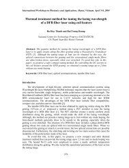
Advances in Optics, Photonics, Spectroscopy & Applications VI ISSN 1859 - 4271The XRD patterns of samples after SiO 2 removal indicate a lesser amount of amorphous SiO 2in comparision with the original samples (line 2 in Figs. 3b, c, d). The XRD patterns of thesamples annealed at 1000 and at 1100 o C after SiO 2 removal show a crystobalite structure – theother form of amorphous SiO 2 when annealed at high temperature. In theory, this annealingprocess at high temperature in inert gas might only change the structure of amorphous SiO 2 andnot the weight because no additional oxygen is provided.In order to investigate the photoluminescence of synthesized materials, we measured thesamples at different stages as following: as-grown, after SiO 2 removal in 5% HF for 10 minutes,and after annealing process at 1000 o C and at 1100 o C in Ar gas for 1 hour after removing SiO 2 .Fig. 4a displays PL images among the as-grown samples with different synthesis times. As canbe seen, PL peaks lie in blue region at 390, 430 nm and one small peak at ~ 480 nm. We alsoobserved a higher intensity on the sample having longer synthesis time. In reality, samples withlonger synthesis times have more SiC nanorods than other samples.Figs. 4b, c are PL of the samples with synthesis times of 2.5 and 3 hours. The lines 1, 2, 3, 4are PL of as-grown, after removing SiO 2 in HF solution, annealed at 1000 o C and at 1100 o C inAr gas after SiO 2 removal respectively. The results show that after removing SiO 2 in 5% HFsolution for 10 minutes the PL intensity changed very little. In contrast, after annealing in inertAr gas at high temperature, the intensity increased noticeably. In both cases, the peaks positionsdid not changed. The only difference is that the PL intensity of sample with longer synthesistime, corresponding with larger amount of produced SiC nanorods, experienced a smaller changeafter annealing at high temperature.Intensity (a.u)(a)150010005001230350 400 450 500Wavelength (nm)1- 2 hours2- 2.5 hours3- 3 hoursIntensity (a.u)(b)15001000500021- As -grown for 2.5 hours2- After remov. SiO 23- Anneal. at 1000 o C4- Anneal. at 1100 o C400 500 600 70031Wavelength (nm)4Intensity (a.u.)(c)10000800060004000200001421- As-grown for 3 hours2- After remov. SiO 23- Anneal. at 1000 o C4- Anneal. at 1100 o C3400 500 600 700542Wavelength (nm)Fig. 4. PL of samples with different synthesized times. a: as-grown samples; b: samplesynthesized for 2.5 hours; c: sample synthesized for 3 hoursThe slight change observed in PL intensity and peak position after removing SiO 2 in 5% HFsolution can be explained by suggesting that the removed part of SiO 2 did not contributesignificantly in the PL emission.With the increase in PL intensity after high-temperature annealing in inert gas it can beassessed as follows: In general, high-temperature annealing in inert gas may reduce some of the
Những tiến bộ trong Quang học, Quang phổ và Ứng dụng VI ISSN 1859 - 4271local stress formed in the growing of shell-core structure SiC nanorods and reduce the defectsthat quench luminescene centers, all of which results in PL intensity increase.The small PL change of the sample with longer synthesis time corresponding with largeramount of produced SiC nanorods can be explained that due to the small amount of defectsappeared in this kind of sample, the annealing process consequently also reduces to a smalleramount of defects, all of which leads to smaller change in PL intensity. With this result, we canstate that the defects in a SiC core (stacking defaults) mainly reduced PL intensity.We observed an interesting phenomenon when comparing the correlation between XRD andPL results after high-temperature annealling. That is, samples that possessed bigger portion ofamorphous SiO 2 also had stronger photoluminescence Fig. 4c). This result leads us to think thatthe oxygen vacancy defects in the amorphous SiO x at the interface of SiO x /SiC played a certainrole in increasing the intensity of the photoluminescence.In comparsion with results made by Li Zhengjiang et al. [12] where they measured two peaksat 410 nm and 490 nm, and our previous work [13] this nanomaterial SiC had PL with blue shiftto shorter wavelength. This shift could have been the result of stacking faults in crystal structureof synthesized SiC nanorods’s core.IV. C<strong>ON</strong>CLUSI<strong>ON</strong>The fabrication of SiC nanorods wrapped by amophous SiO 2 was made by carbothermalreduction without any catalyst. The synthesized material emits blue PL in 390-480 nm region atroom temperature. The intensity and PL peak positions did not change after removing SiO 2 butincreased after annealing at high temperature show that related luminescence centers mainlyoriginate from SiC core and in SiC/SiO 2 interfaces.V. ACKNOWLEDGMENTSThe authors wish to thank their colleagues Dr. Tran Dang Thanh, Dr Nguyen Duc Van, DoHung Manh, Nguyen Thi Thu Trang, Nguyen Anh Tuan at the Institute of Materials Science fortheir help in optical and structure measurements. This work is supported by the Foundation forScience and Technology Development (Project No. 103.02.70.09) and The National KeyLaboratory for Electronic materials and devices of the Institute of Materials Science.REFERENCES[1] L.T. Canham, Appl. Phys. Lett. 57 (1990)1046-1048[2] T. Matsumoto, J. Takahashi, T. Tamaki, Toshiro Futagi. Appl. Phys. Lett 64(2),(1994) 226-228[3] L. Rebohle, T. Gebel, H. Frob, H. Reuther, W. Skorupa. Appl. Surface Science 184 (2001), 156-160[4] D. Chen, Z. M. Liao, L. Wang, F. Zhao, W.Y. Cheung, S.P. Wong. Opt. materials 23(2003) 65-69[5] K. F. Cai, A. X. Zhang, J. L. Yin H. F. Wang, X. H Yuan. Appl. Phys. A 91 (2008) 579-584[6] B.-C. Kang, S.-B. Lee, J. –H. Boo. Thin Solid Films 464-465 (2004) 215-219[7] H Wang, Zh. Xie, W. Yang, J.Fang, L. An. Crystal Growth & Design Vol 8, N o 11(2008), 3893-3896[8] W. Shi, Y. Zheng, H.Peng, N Wang, Ch. S. Lee, S. T. Lee, J. Am Ceram. Soc. 83 (2000) 3228-3230.[9] J. Zhu, H. Wu, H. T. Chen, X. L. Wu, X. Xiong. Physics Letters A 373 (2009) 1697-1700[10] X.J. Wang, J.F. Tian, L.H. Bao, T.Z. Yang, C. M. Shen, H. J.Gao. J. Appl. Physics 102, (2007),[11] G.W. Meng, et al., Metallurgical and Materials transactions A, Volume 30A, (1999), p. 213.[12] Zh. Li, W. Gao. A. Meng, Z. Geng, L. Gao. J. Phys. Chem. 113 (2009) 91-thảo luận[13] Huynh Th. Ha, et al. IJ. Nanotechnology, Vol 8 , No 3/4/5(2011) 324-334543
- Page 1 and 2:
Những tiến bộ trong Quang h
- Page 3 and 4:
Những tiến bộ trong Quang h
- Page 5 and 6:
Những tiến bộ trong Quang h
- Page 8:
Advances in Optics, Photonics, Spec
- Page 12 and 13:
Advances in Optics, Photonics, Spec
- Page 14 and 15:
Advances in Optics, Photonics, Spec
- Page 16 and 17:
Advances in Optics, Photonics, Spec
- Page 18:
Advances in Optics, Photonics, Spec
- Page 21 and 22:
Những tiến bộ trong Quang h
- Page 23 and 24:
Những tiến bộ trong Quang h
- Page 25:
Những tiến bộ trong Quang h
- Page 28 and 29: Advances in Optics, Photonics, Spec
- Page 30 and 31: Advances in Optics, Photonics, Spec
- Page 32 and 33: Advances in Optics, Photonics, Spec
- Page 34 and 35: Advances in Optics, Photonics, Spec
- Page 36 and 37: Advances in Optics, Photonics, Spec
- Page 38 and 39: Advances in Optics, Photonics, Spec
- Page 40 and 41: Advances in Optics, Photonics, Spec
- Page 42 and 43: Advances in Optics, Photonics, Spec
- Page 44 and 45: Advances in Optics, Photonics, Spec
- Page 46: Advances in Optics, Photonics, Spec
- Page 50 and 51: Advances in Optics, Photonics, Spec
- Page 53 and 54: Những tiến bộ trong Quang h
- Page 55 and 56: Những tiến bộ trong Quang h
- Page 57 and 58: Những tiến bộ trong Quang h
- Page 59 and 60: Những tiến bộ trong Quang h
- Page 61 and 62: Những tiến bộ trong Quang h
- Page 63 and 64: Những tiến bộ trong Quang h
- Page 65 and 66: Những tiến bộ trong Quang h
- Page 68 and 69: Advances in Optics, Photonics, Spec
- Page 70 and 71: Advances in Optics, Photonics, Spec
- Page 72 and 73: Advances in Optics, Photonics, Spec
- Page 74 and 75: Advances in Optics, Photonics, Spec
- Page 76 and 77: Advances in Optics, Photonics, Spec
- Page 80 and 81: Advances in Optics, Photonics, Spec
- Page 82 and 83: Advances in Optics, Photonics, Spec
- Page 84 and 85: Advances in Optics, Photonics, Spec
- Page 86 and 87: Advances in Optics, Photonics, Spec
- Page 88 and 89: Advances in Optics, Photonics, Spec
- Page 90 and 91: Advances in Optics, Photonics, Spec
- Page 92 and 93: Advances in Optics, Photonics, Spec
- Page 94 and 95: Advances in Optics, Photonics, Spec
- Page 96 and 97: Advances in Optics, Photonics, Spec
- Page 98 and 99: Advances in Optics, Photonics, Spec
- Page 100 and 101: Advances in Optics, Photonics, Spec
- Page 102 and 103: Advances in Optics, Photonics, Spec
- Page 104 and 105: Advances in Optics, Photonics, Spec
- Page 106 and 107: Advances in Optics, Photonics, Spec
- Page 108 and 109: Advances in Optics, Photonics, Spec
- Page 110 and 111: Advances in Optics, Photonics, Spec
- Page 112 and 113: Advances in Optics, Photonics, Spec
- Page 114 and 115: Advances in Optics, Photonics, Spec
- Page 116 and 117: Advances in Optics, Photonics, Spec
- Page 118 and 119: Advances in Optics, Photonics, Spec
- Page 120 and 121: Advances in Optics, Photonics, Spec
- Page 122 and 123: Advances in Optics, Photonics, Spec
- Page 124 and 125: Advances in Optics, Photonics, Spec
- Page 126 and 127: Advances in Optics, Photonics, Spec
- Page 128 and 129:
Advances in Optics, Photonics, Spec
- Page 130 and 131:
Advances in Optics, Photonics, Spec
- Page 132 and 133:
Advances in Optics, Photonics, Spec
- Page 134 and 135:
Advances in Optics, Photonics, Spec
- Page 136 and 137:
Advances in Optics, Photonics, Spec
- Page 138 and 139:
Advances in Optics, Photonics, Spec
- Page 140 and 141:
Advances in Optics, Photonics, Spec
- Page 142 and 143:
Advances in Optics, Photonics, Spec
- Page 144 and 145:
Advances in Optics, Photonics, Spec
- Page 146 and 147:
Advances in Optics, Photonics, Spec
- Page 148 and 149:
Advances in Optics, Photonics, Spec
- Page 150 and 151:
Advances in Optics, Photonics, Spec
- Page 152 and 153:
Advances in Optics, Photonics, Spec
- Page 154:
Advances in Optics, Photonics, Spec