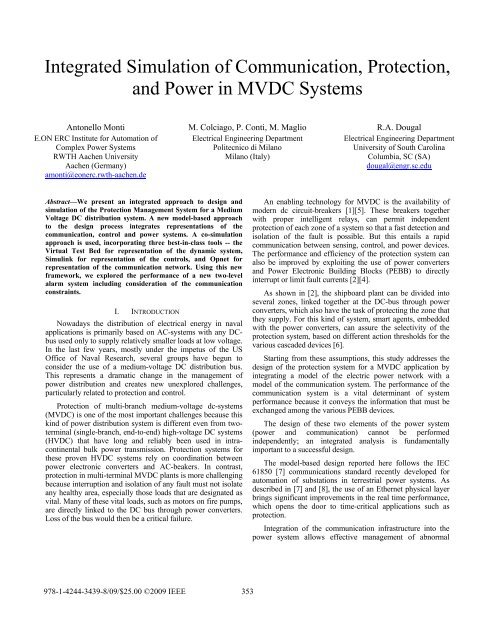
Integrated Simulation of Communication, Protection, and Power in ...
Integrated Simulation of Communication, Protection, and Power in ...
Integrated Simulation of Communication, Protection, and Power in ...

Create successful ePaper yourself
Turn your PDF publications into a flip-book with our unique Google optimized e-Paper software.
for the 10 kHz switch<strong>in</strong>g frequency <strong>of</strong> the PEBB. The dataacquired for the control system are the same as <strong>in</strong> the previousstage.Each bus feeds two k<strong>in</strong>ds <strong>of</strong> loads: vital loads (100 kW)<strong>and</strong> non-vital ones (50 kW). A vital load can be supplied fromeither the starboard bus or the port bus but not by both buses atthe same time. Auctioneer<strong>in</strong>g diodes affect this function. Thetwo buses are kept at different voltages (800 V-750 V) so thatif a cont<strong>in</strong>gency occurs on the primary bus that causes thevoltage to drop, then the auction<strong>in</strong>g diode allows the load tobe picked up by the secondary bus. By <strong>in</strong>creas<strong>in</strong>g the outputvoltage <strong>of</strong> the backup converter, the load can be re<strong>in</strong>stated t<strong>of</strong>ull operat<strong>in</strong>g voltage. The loads are represented by an ideal<strong>in</strong>verter that feeds a constant power three phase load (thiscould represent a low power drive such as a pump).Figure 3: <strong>Power</strong> Supply areaThe switch<strong>in</strong>g-averaged models <strong>of</strong> the buck convertersobviously do not produce any switch<strong>in</strong>g ripple, but the LCsecond order output filters do present dynamics that areimportant <strong>in</strong> assess<strong>in</strong>g the effectiveness <strong>of</strong> the protectionscheme. These filters have been designed to give 80 dBsuppression at the 1 kHz switch<strong>in</strong>g frequency which leads to acut-<strong>of</strong>f frequency at 10 Hz. Every capacitor is also providedwith a DC circuit breaker that prevents current from flow<strong>in</strong>g<strong>in</strong>to a fault.For each group <strong>of</strong> converters the follow<strong>in</strong>g measurementsare acquired: the <strong>in</strong>ductor current, the capacitor voltage <strong>and</strong>the output current. These are sent to the controller, which isrepresented with<strong>in</strong> Simul<strong>in</strong>k.In Figure 3 are represented two groups <strong>of</strong> conversions, onefor each bus. This scheme refers to the bow section but it isthe same also for the one <strong>in</strong> the astern.Figure 4: low voltage area<strong>Power</strong> Electronic Build<strong>in</strong>g Blocks (PEBBs) have beenemployed to represent the step-down converter. As it wasshown for the rectifiers, two PEBBs connected <strong>in</strong> series createa bipolar 800 V DC l<strong>in</strong>k. In this case the LC filter is designed355Figure 5: high voltage areaIn the high voltage area, three PEBBs have been used todef<strong>in</strong>e a three phase <strong>in</strong>verter. These are aga<strong>in</strong> switch<strong>in</strong>gaverage models controlled by three s<strong>in</strong>e wave referencesshifted by 120° one from the other. The load is modeled byanother constant power component. The rated power <strong>of</strong> thisload is 20 MW <strong>and</strong> represents one <strong>of</strong> the propulsion motors <strong>of</strong>the ship. This motor is fed from both the buses <strong>in</strong> order to splitthe current <strong>and</strong> to m<strong>in</strong>imize voltage losses.IV. RECONFIGURABLE CONTROL MODELAs described before, the two ma<strong>in</strong> buses are fed through apower conversion stage consist<strong>in</strong>g <strong>of</strong> an ac-dc conversion <strong>and</strong>a dc-dc buck conversion.The first stage (i.e. ac-dc conversion) is made by anuncontrolled diode bridge. The second stage consists <strong>of</strong> a dcdcbuck converter made based on power electronic build<strong>in</strong>gblock (PEBB) modules. This buck converter permitsregulation <strong>of</strong> the system voltage <strong>and</strong> control <strong>of</strong> the output
current while at the same time provid<strong>in</strong>g protection featuresthanks to a reconfigurable control architecture.An averaged model <strong>of</strong> the buck converter is the PEBBelement used <strong>in</strong> the VTBpro schematic which receives therectified voltage <strong>and</strong> the desired duty cycle as <strong>in</strong>puts, <strong>and</strong>provides an ideal dc-dc conversion at the output port.This power converter has a switch<strong>in</strong>g frequency <strong>of</strong> only1kHz, consider<strong>in</strong>g the very high rated power. Notice that,because an averaged model is used, this step down convertercould at the same time represent either a traditional bucktopology or a more-sophisticated resonant converter, based onsuitable choice <strong>of</strong> the parameters. In this second case, thisstage could provide also galvanic <strong>in</strong>sulation as described <strong>in</strong> the<strong>in</strong>troduction.Figure 7: Control SchematicFigure 6: Converter implementation <strong>in</strong> VTBProSo the task <strong>of</strong> the system control is to provide anappropriate duty cycle to the PEBB element <strong>in</strong> order to satisfythe desired requirements <strong>of</strong> voltage regulation <strong>and</strong> outputcurrent control. A proper coord<strong>in</strong>ation <strong>of</strong> the two loops canalso provide protection features <strong>in</strong> the system control. Ineffect, four work<strong>in</strong>g conditions have been identified:• Normal condition: no faults or overload are detectedby the control system; hence the voltage control only operatesto establish the pre-def<strong>in</strong>ed voltage at the output <strong>of</strong> the PEBB<strong>and</strong> the current is with<strong>in</strong> the normal limits.• Low-risk level: the devices detect an anomaly that isnot classified as a failure. The control system acts to ma<strong>in</strong>ta<strong>in</strong>the operat<strong>in</strong>g voltage at its rated value with a fast <strong>and</strong> stableresponse <strong>and</strong> the current itself is ma<strong>in</strong>ta<strong>in</strong>ed with<strong>in</strong> securelevels.• High-risk level: the device that detects a failure acts<strong>in</strong>stantaneously without wait<strong>in</strong>g on any other communications.This immediately reconfigures the PEBB to operate <strong>in</strong> currentlimit<strong>in</strong>gmode.• Overall protections: the gate signals are <strong>in</strong>hibited <strong>and</strong>the converter completely disconnects.Figure 7 represents the control system for the buckconverter.There are two loops: the first is the voltage-external loop<strong>and</strong> the second is the <strong>in</strong>ner-current loop.Voltage loop: the output buck voltage is compared to areference value thus generat<strong>in</strong>g a signal error. The VoltagePID provides a feedback control signal which is a referencevalue for the output current. The Voltage PID <strong>in</strong>creases thephase marg<strong>in</strong> at the crossover frequency <strong>of</strong> the voltage loopprovid<strong>in</strong>g stability <strong>and</strong> <strong>in</strong>creases the low-frequency loop ga<strong>in</strong>such that the output voltage is better regulated at dc <strong>and</strong> atfrequencies far below the crossover frequency.Current loop: the comparison between the measuredcurrent <strong>and</strong> the reference current gives an error signal which isprocessed by the Current PI controller thus obta<strong>in</strong><strong>in</strong>g theaveraged duty cycle; the gate driver provides the pulses for theconverter.The switch shown <strong>in</strong> the bottom <strong>of</strong> the schematic allowsthe switch<strong>in</strong>g to current-limit<strong>in</strong>g operation.When a high risk level event is detected, a signal from thecommunication <strong>and</strong> protection system is sent to the switch <strong>in</strong>order to limit the fault current <strong>and</strong> to prevent damage to theconverter.The possibility <strong>of</strong> us<strong>in</strong>g the buck control system forprotection leads to a higher survivability <strong>of</strong> the electric plant.The voltage control loop assure ma<strong>in</strong>tenance <strong>of</strong> the ratedvoltage <strong>in</strong> every normal <strong>and</strong> non-fault situation, while thecurrent control loop limits the output current when a dc busfault occurs.V. COMMUNICATION INFRASTRUCTURE MODELINGConsider<strong>in</strong>g that the communication <strong>in</strong>troduces delay <strong>in</strong>the reaction time <strong>of</strong> the system, it is important to design <strong>of</strong> theprotection architecture consider the several different levels <strong>of</strong>risk. At least two levels must be considered:• High-risk level (correspond<strong>in</strong>g to the third <strong>and</strong> fourthoperat<strong>in</strong>g modes <strong>of</strong> the converter): the device that detects thefailure acts <strong>in</strong>stantaneously without wait<strong>in</strong>g any othercommunications.356
• Low-risk level (correspond<strong>in</strong>g to the secondoperat<strong>in</strong>g mode <strong>of</strong> the converter): the devices detect ananomaly that is not classified as a failure. S<strong>in</strong>ce they areunable to make an optimal decision, they exchange data withneighbor<strong>in</strong>g devices about the type <strong>of</strong> anomaly detected <strong>in</strong>order to reach a shared solution. Dur<strong>in</strong>g this stage, the deviceautomatically switches <strong>in</strong>to a state <strong>of</strong> alert, wait<strong>in</strong>g for a f<strong>in</strong>aldecision.The category <strong>of</strong> risk is identified by analyz<strong>in</strong>g thefollow<strong>in</strong>g characteristics <strong>of</strong> a given waveform:1) peak <strong>in</strong>stantaneous value2) wavelet-based analysis <strong>of</strong> the transient waveformThe comb<strong>in</strong>ation <strong>of</strong> these two key elements allowsreach<strong>in</strong>g a higher level <strong>of</strong> selectivity. The idea is to identifydifferent thresholds for the peak <strong>in</strong>stantaneous values able totrigger different operat<strong>in</strong>g modes <strong>of</strong> the protection devices:1) highest threshold: immediate protection,reconfiguration <strong>of</strong> the power electronic devices to operate <strong>in</strong>current-limit<strong>in</strong>g operation2) one or more m<strong>in</strong>or thresholds that triggers the timefrequencyanalysis <strong>and</strong> the data exchange with the neighbors.While the first level deals with the classical idea <strong>of</strong>protection, the second level <strong>in</strong>troduces the possibility <strong>of</strong>manag<strong>in</strong>g more complex situations or also to detect <strong>in</strong>cipientfaults.A. <strong>Communication</strong> architecture simulationThe communication delay is estimated us<strong>in</strong>g the discreteevent simulator Opnet Modeler 14.5 (see Figure 8).<strong>Simulation</strong> models are divided <strong>in</strong> hierarchy that consist<strong>in</strong>g<strong>of</strong> three ma<strong>in</strong> levels: Start<strong>in</strong>g from the bottom there is theProcess Model, that consists <strong>of</strong> F<strong>in</strong>ite State Mach<strong>in</strong>e (FMS), Ccode <strong>and</strong> ProtoC function that def<strong>in</strong>e how the process is ableto react to an event that happens <strong>in</strong> the system, <strong>and</strong> where ispossible to characterize the connection with the other process.The second level is the Node Model that is an organized set <strong>of</strong>modules describ<strong>in</strong>g the various functions <strong>of</strong> each node. Eachnode is implemented by process model. The top part <strong>of</strong> thehierarchical construction is the Network Model that def<strong>in</strong>esthe network layout <strong>and</strong> characterizes the node attributes for aparticular scenario.Opnet permits extension <strong>of</strong> its library <strong>and</strong> so it is possibleto call Matlab functions directly from the process model.Figure 8: OPNET Matlab Co-<strong>Simulation</strong><strong>Communication</strong>s are based on IEC61850 GOOSEmessag<strong>in</strong>g (Generic Object Oriented Substation Events). Thischoice has several features that are important for the system.First <strong>of</strong> all, the message is directly published on the Ethernetlayer <strong>and</strong> there is the possibility <strong>of</strong> choos<strong>in</strong>g the priority levelto move the message at the beg<strong>in</strong>n<strong>in</strong>g <strong>of</strong> the queue messagefrom an Ethernet switch. Another important feature is thatGOOSE messages can be multicast so all the power converterscan be alerted at the same time, but can also possible create aVirtual LAN, by add<strong>in</strong>g 4 bytes to the Ethernet data frame perthe IEEE 802.IQ st<strong>and</strong>ard, to restrict the dataflow.Because the message is sent from the transmitter withoutcerta<strong>in</strong>ty that the power converter receiver is free <strong>in</strong> thatmoment, there is no guarantee that a message will arrive at theIED. For this reason the st<strong>and</strong>ard IEC61850 def<strong>in</strong>es arepetition mechanism that def<strong>in</strong>es a <strong>in</strong>cremental frequency forsend<strong>in</strong>g until the receiver IED answers it to stop or after 1second.Figure 9: <strong>Communication</strong> network modelFigure 9 shows the Opnet simulation network. On the leftthere is the <strong>Communication</strong> block. It is the block that givesStart/Stop comm<strong>and</strong>s to the Matlab/Simul<strong>in</strong>k simulation <strong>and</strong>manages the exchange <strong>of</strong> the data vector <strong>of</strong> the state condition<strong>of</strong> all the power converters.Moreover the data vector <strong>in</strong>cludes also the Simul<strong>in</strong>ksimulation time. The l<strong>in</strong>k between <strong>Communication</strong> box <strong>and</strong>the Hub is made by one ad Hoc l<strong>in</strong>k, without communicationdelay. The aim <strong>of</strong> the simulation is to evaluate the end to endcommunication delay <strong>in</strong> which a signal starts from a powerconverter <strong>in</strong> a faulted state <strong>and</strong> reaches all the other powerconverters through a switch.When a fault happens, the <strong>Communication</strong> block sends thepacket to the HUB block that reads every state from the packet<strong>and</strong> it sends to each PEBB block a vector summariz<strong>in</strong>g thestatus <strong>of</strong> each converter. The status <strong>of</strong> each converter isrepresented by an <strong>in</strong>teger number..In order to have a redundant structure, a star topologyarchitecture is built with two switches (one per side <strong>of</strong> theship) that connects all the power converters ( four on thestarboard side <strong>and</strong> four on the port side), through an EthernetL<strong>in</strong>k, creat<strong>in</strong>g an Ethernet LAN.357
F<strong>in</strong>ally, the delay calculated <strong>in</strong> OpNet is passed toSimul<strong>in</strong>k, that will <strong>in</strong>sert a proper delay before acquir<strong>in</strong>g the<strong>in</strong>formation.Let us now take a more detailed look at this process.As show <strong>in</strong> Figure 10, the process starts <strong>in</strong> the Init state,underl<strong>in</strong>ed by a big black arrow. The aim <strong>of</strong> this state is todirectly open the Matlab eng<strong>in</strong>e with the Matlab functionengOpen() <strong>and</strong> also to <strong>in</strong>itialize all the variables <strong>in</strong> bothsimulation programs. For example there is a function thatcreates the array that permits data to be exchanged with theMatlab eng<strong>in</strong>e. Before end<strong>in</strong>g his work, this state asks to startthe electric simulation for a first step time. For the currentanalysis a time step <strong>of</strong> 1ms is used. Notice that this determ<strong>in</strong>esthe rate <strong>of</strong> exchange <strong>of</strong> simulation data between OpNet <strong>and</strong>Simul<strong>in</strong>k, but Simul<strong>in</strong>k could actually perform more than onestep for each call.the Evaluate state generates an <strong>in</strong>terrupt <strong>and</strong> the eventSEND_DATA happens.This br<strong>in</strong>gs the process to the Process<strong>in</strong>g state <strong>and</strong> thefunction Psend() is performed. This function writes the statecondition <strong>of</strong> the electric power converter <strong>in</strong>to the packetstructure <strong>and</strong> it sends the data packet to the Hub with a stream<strong>in</strong>terrupt through the node transmitter as shown <strong>in</strong> Figure 11.At this po<strong>in</strong>t the <strong>Communication</strong> block waits <strong>in</strong> the Process<strong>in</strong>gstate until the delay time is expired.When the Receiver node receives the packet, anotherstream <strong>in</strong>terrupt is called <strong>and</strong> the event ARRIVAL_DATAhappens. So, the function Preceive() reads the delay time fromthe new packet <strong>and</strong> adds that to the Matlab time simulation.This calculation def<strong>in</strong>es when the fault has to be sent to thepower converter. After that, it schedules the self <strong>in</strong>terrupt thatsends this data <strong>and</strong> the communication block returns <strong>in</strong> theIdle state.VI. PRELIMINARY SIMULATION RESULTSAll the components <strong>of</strong> the simulation have been fullydeveloped. Currently the authors are work<strong>in</strong>g at the test<strong>in</strong>gphase. Nevertheless, some prelim<strong>in</strong>ary results are alreadyavailable <strong>and</strong> demonstrate the capabilities <strong>of</strong> the system.In Figure 12 <strong>and</strong> 13 an example <strong>of</strong> transient is reported.Figure 10: Process modelFigure 12: Current transient dur<strong>in</strong>g faulty conditionFigure 11: <strong>Communication</strong> node blockThis node is not forced <strong>and</strong> so, when every comm<strong>and</strong> isdone, the process passes directly to the next state (idle state),without wait<strong>in</strong>g for any particular event.Here, the default condition is to wait until the end <strong>of</strong> thestep time, when the event END_TIME happens, the functiontime_misure() records the simulation.So the process alternates between Idle state <strong>and</strong> Evaluatestate. While <strong>in</strong> Evaluate state, a new step <strong>of</strong> the systemsimulation is performed. If one IED detects a fault condition,Figure 13: Duty Cycle transient dur<strong>in</strong>g faulty condition358
Analyz<strong>in</strong>g these figures it is possible to identify asequence <strong>of</strong> status:• <strong>in</strong> the first second <strong>of</strong> simulation the voltage control br<strong>in</strong>gsthe system to the nom<strong>in</strong>al operat<strong>in</strong>g po<strong>in</strong>t.• between the first <strong>and</strong> fifth second the system operatesnormally• around the fifth second a fault determ<strong>in</strong>e a violent change<strong>in</strong> the current absorbed• the system reacts <strong>and</strong> switches from voltage control tocurrent limited controlWhile Figure 12 reports the current behavior, Figure 13reports the output <strong>of</strong> the controllers <strong>of</strong> the converter i.e. theduty cycle.VII. CONCLUSIONSThe paper presented an experience <strong>in</strong> the design <strong>of</strong> theprotection architecture for an MVDC system. Here, <strong>in</strong>particular, we focused on the model<strong>in</strong>g challenges. In order tohave reliable models, it is important to <strong>in</strong>tegrate the simulation<strong>of</strong> the power system with the control <strong>and</strong> the communication<strong>in</strong>frastructure. This result has been achieved here by<strong>in</strong>tegrat<strong>in</strong>g VTBPro with Simul<strong>in</strong>k <strong>and</strong> OpNet.ACKNOWLEDGMENTThis work was supported by the US Office <strong>of</strong> NavalResearch under the Grant N00014-07-1-0603. The authorsalso thank OpNet Technologies who provided licenses <strong>and</strong>support for the network communication simulation.REFERENCES[1] Christoph Meyer, Maurice Kowal, Rik W. De Doncker, “ CircuitBreaker Concepts for Future High- <strong>Power</strong> DC-Application”Industry Applications Conference, 2005. Fourtieth IAS AnnualMeet<strong>in</strong>g. Conference Record <strong>of</strong> the 2005[2] Mesut E. Baran, Nikhil R. Mahajan, “ Overcurrent <strong>Protection</strong> onVoltage-Source-Converter-Based Multiterm<strong>in</strong>al DC DistributionSystems” IEEE Trans. on <strong>Power</strong> Delivery, vol. 22, No. 1, Jan. 2007[3] Mesut E. Baran, Nikhil R. Mahajan, “ PEBB Based DC System<strong>Protection</strong>: Opportunities <strong>and</strong> Challenges” Transmission <strong>and</strong>Distribution Conference <strong>and</strong> Exhibition, 2005/2006 IEEE PES[4] Mesut E. Baran, Nikhil R. Mahajan, A. W. Kelley, “ Use <strong>of</strong> PEBBConverters as Current Limit<strong>in</strong>g Circuit Breakers ” submitted to IEEETransaction on PELS, Aug. 2004[5] Slobodan Krstic, Edward L. Wellner, Ashish R. Bendre, BorisSemenov “ Circuit Breaker Technologies for Advance Ship<strong>Power</strong> Systems ” Electric Ship Technologies Symposium, 2007. ESTS'07. IEEE[6] Mesut E. Baran, Nikhil R. Mahajan, “ System Reconfiguration onShipboard DC Zonal Electrical System” Electric ShipTechnologies Symposium, 2005 IEEE[7] A. Apostolov, C. Brunner, <strong>and</strong> K. Cl<strong>in</strong>ard, “Use <strong>of</strong> IEC 61850 objectmodels for power system quality/security data exchange” Quality <strong>and</strong>Security <strong>of</strong> Electric <strong>Power</strong> Delivery Systems, 2003. CIGRE/ PES2003. CIGRE/IEEE PES International Symposium[8] T. Skeie, S. Johanessen, <strong>and</strong> C. Brunner, “ETHERNET <strong>in</strong> substationautomation” IEEE Control Syst. Mag., vol. 22, no. 3, pp. 43–51,Jun. 2002.[9] <strong>Communication</strong> Networks <strong>and</strong> Systems <strong>in</strong> substations 2003, IEC61850, 1 st ed.359