WAVE SOLDERING REFLOW SOLDERING SELECTIVE ... - SMTA
WAVE SOLDERING REFLOW SOLDERING SELECTIVE ... - SMTA
WAVE SOLDERING REFLOW SOLDERING SELECTIVE ... - SMTA

Create successful ePaper yourself
Turn your PDF publications into a flip-book with our unique Google optimized e-Paper software.
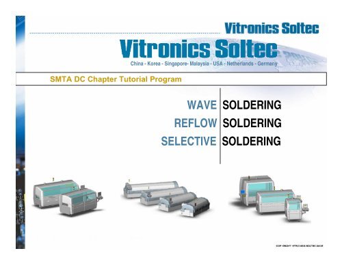
<strong>SMTA</strong> DC Chapter Tutorial ProgramChina - Korea - Singapore- Malaysia - USA - Netherlands - Germany<strong>WAVE</strong> <strong>SOLDERING</strong><strong>REFLOW</strong> <strong>SOLDERING</strong><strong>SELECTIVE</strong> <strong>SOLDERING</strong>
Status of RoHSLead Free Implementation inNorth AmericaTrials and Tribulations
Challenges in AssemblySolderability issuesFlux PenetrationSolving voiding issues due to entrapped flux gasesAchieving theperfect joint!Identifying Warpage as an Issue with lead free reflow.
Materials
IPC/JEDEC Moisture SensitivityLevels (MSL)Any absorbed moisture is quickly turned into superheatedsteam in lead-free reflow.SMD components are prone to popcorn cracking since:Thin and therefor low fracture strength.Absorb moisture more easily.Leads transfer the high temperatures to the package.
Delamination of ComponentsSonoscan technology used to observedelamination of components.Pictures left: flip chip device on top of the BGA.The sonoscan results showed delamination of theinterface between underfill and the substrate.The delaminated area provides a path for electromigrationor current leakage.Upon thermal cycling, solder may creep into thedelaminated area whereby weakening thesolder joints or creating a bridge.A possible cause for this type of defect is moistureevaporation during reflow. Baking or drying theparts before assembly should prevent thedelamination from occuring.
Temperature ExposureRe-qualification of MSLratings.Higher vapour pressure inthe package.Higher thermal mismatch.Decreasing adhesion alongthe internal interfaces.Higher failure rate becauseof delamination and cracks.225C250C
Case StudyTHE PROBLEMImproper joint formation during a lead freewave process.
Board Characterization Drilling characteristics Plating thickness by XRF and dissolution techniquesTable 1. Thickness of Surface Finish (Micro Inches)Topside Pad Bottom Side Pad Barrel -1 Barrel 2Average 88.94 ± 16.44 63.97 ± 12.72 48.73 ± 9.12 38.02 ± 11.12 recommended levels: 4 - 20 mils (MacDermid)8 - 12 mils (EMS)
Failure Analysis Using X-Section
Failure Analysis Using SEM-EDX Evidence of Imm. Silver Finish Evidence of exposed Copper
Solderability TestingSAC 305SnPb Using IPC specifications, we evaluated thesolderability of the plating with both tin leadand lead free
Findings and Outcome Plating was poorly and unevenly applied. Resulting in unacceptable solderability. This illustrates the challenges lead free willhave on the US market. Inexperience andlack of knowledge will impact assembly inmany different ways.
Todays Reality Materials and equipment will directlyinfluence you ability and capacity toassemble lead free products. Careful selection of materials will givean understanding of the challengeslead free will present to your company. Equipment design will either challengeor enable your company to implementlead free processes.
Mixed Technology
The Transition to Lead Free