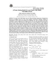
70 Patel and Kshirsagarfactor F. <strong>Design</strong> techniques to reduce the phase noise dueto the circuit have been widely studied and investigated inrecent years. We are reducing noise <strong>by</strong> following methods.A. <strong>Noise</strong> filteringThe use <strong>of</strong> an on-chip LC filter can effectively suppressthe noise from the tail transistor. Fig. 1 shows the schematic<strong>of</strong> a <strong>VCO</strong> with the noise filter to suppress the noise <strong>of</strong> thetail current transistor. The capacitor C fprovides a lowimpedance path for the noise at 2f 0<strong>of</strong> the tail currenttransistor. The inductor L fensures a high impedancecommon node for the differential pair. The big <strong>of</strong>f-chipinductor L Ifdegenerates the low frequency noise <strong>by</strong> the2factor |1 jgm LF| , where g mis the transconductance <strong>of</strong>the tail transistor.Fig. 3 shows a LC <strong>VCO</strong> with harmonic tuned LC tankand its output voltage waveform. The output voltage <strong>of</strong> a<strong>VCO</strong> with harmonic tuned LC include both the fundamentaland the third harmonic frequency component and has awaveform more like a square wave. Therefore, the slope <strong>of</strong>the output voltage <strong>of</strong> a <strong>VCO</strong> with harmonic tuned tank issteeper than that <strong>of</strong> a standard LC <strong>VCO</strong> and the phasenoise is reduced.Fig. 1. A LC <strong>VCO</strong> with the noise filter.B. Harmonic tuned LC tankAs described <strong>by</strong> Hajimili'e phase noise model, the mostnoise-sensitive moment <strong>of</strong> <strong>VCO</strong>s is the zero crossing point<strong>of</strong> the <strong>VCO</strong> output voltage. The phase noise resulting froma noise injected around the zero crossing point isproportional to the voltage slope at the zero crossing point.Therefore, increasing the slope <strong>of</strong> <strong>VCO</strong> output voltage canreduce phase noise. Therefore, increasing the slope <strong>of</strong> <strong>VCO</strong>output voltage can reduce phase noise.Fig. 3. A complementary <strong>VCO</strong> with LC tuned tank: (a)schematic and (b) output voltage waveform.III. CMOS LAYOUT DESIGNINGA. Layout <strong>of</strong> <strong>Noise</strong> filtering circuitFig. 2. A differential tuning LC <strong>VCO</strong>.Fig. 4. Layout <strong>of</strong> <strong>Noise</strong> filtering circuit.
B. Layout <strong>of</strong> Harmonic tuned circuitPatel and Kshirsagar 71In both simulation results, the variation in capacitancevalue is shown as the dimension is reducing and the value<strong>of</strong> capacitance is increasing. Due to which the value <strong>of</strong> Lis decrasing. Reduction in L will help to decrease the noiseacross <strong>PLL</strong>. All the results are taken at W = 0.1 m andL = 0.01 m.Fig. 5. Layout <strong>of</strong> Harmonic Tuned Circuit.III. RESULTS AND ANALYSISTwo method for reducing noise have been studied. Forlow noise <strong>PLL</strong> we designed filter noise circuit and Harmonictuned circuit. Since <strong>PLL</strong> were presented whichsimultaneously achieve high operating frequency and goodphase noise through the use <strong>of</strong> several innovativearchitectural and circuit design techniques. These circuits,through simulation, measurement, demonstrated performanceand speed in a gigahertz range which till date has not beenrealized in a conventional CMOS process. The designedcircuit have analysed with required parameter for reducingthe noise <strong>of</strong> <strong>PLL</strong>.Fig. 6. Nmos W = 0.900, L = 0.120 mIV. CONCLUSIONThe main focus <strong>of</strong> this paper was to design the lownoise CMOS <strong>PLL</strong>. The dominated phase noise source in a<strong>PLL</strong> are different type <strong>of</strong> block like <strong>VCO</strong>, Tuned Circuit etc.Understanding the generating mechanism <strong>of</strong> phase noisein <strong>VCO</strong> and other <strong>PLL</strong> blocks is the theoretic basis to designlow phase noise <strong>PLL</strong>s. In this paper, the phase noisemechanism <strong>of</strong> <strong>VCO</strong>s, including both <strong>of</strong> ring oscillator based<strong>VCO</strong> and LC tank based <strong>VCO</strong>, were deeply studied andanalyzed.REFRENCES[1] A.A. Abidi, "High-frequency noise measurements on FET'swith small dimensions," IEEE Trans. Electron Devices, vol.ED-33, pp. 1801-1805, Nov. (1986).[2] R.P. Jindal, "Hot-electron effects on channel thermal noisein fineline NMOS field-effect transistors," IEEE Trans.Electron Devices, vol. ED-33, pp. 1395-1397, Sept. (1986).[3] B. Wang, J.R. Hellums, and C.G. Sodini, "MOSFET thermalnoise modeling for analog integrated circuits," IEEE J.Solid-State Circuits, vol. 29, pp. 833-835, July (1994).[4] S. Sheng et al., "A low-power CMOS chipset for spreadspectrumcommunications," in ISSCC Dig. Tech. Papers,(1996), vol. 39, pp. 346-347.[5 E. Heaney et al., "Ultra low power low noise amplifiersfor wireless communications," in GaAs-IC Symp. Dig. Tech.Papers, (1993), pp. 49-51.[6] R.P. Jindal, "<strong>Noise</strong> associated with distributed resistance <strong>of</strong>MOSFET gate structures in integrated circuits," IEEE Trans.Electron Devices, vol. ED-31, pp. 1505-1509, Oct. (1984).[7] A. van der Ziel, "<strong>Noise</strong> in solid-state devices and lasers,"Proc. IEEE, vol. 58, pp. 1178-1206, Aug. (1970).[8] "A 320 MHz CMOS <strong>PLL</strong> for microprocessor clockgeneration," IEEE J. Solid-State Circuits, vol. 31, pp. 1715-1722, Nov. (1996).[9] I.A. Young, "A <strong>PLL</strong> clock generator with 5-110 MHz lockrange for microprocessors," IEEE J. Solid-State Circuits,vol. 27, pp. 1599-1607,Nov. 1992.[10] J. Maneatis, "<strong>Low</strong>-jitter process independent DLL and <strong>PLL</strong>based on self-biased techniques," IEEE J. Solid-StateCircuits, vol. 31, pp. 1723-1732, Nov. 1996.Fig. 7. Nmos W = 1.020, L = 0.120 m