High-Speed SiGe BiCMOS Technologies - University of Toronto
High-Speed SiGe BiCMOS Technologies - University of Toronto
High-Speed SiGe BiCMOS Technologies - University of Toronto

You also want an ePaper? Increase the reach of your titles
YUMPU automatically turns print PDFs into web optimized ePapers that Google loves.
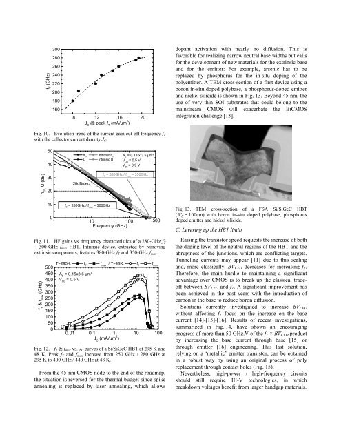
f T(GHz)3002802602402202001801608 12 16 20J C@ peak f T(mA/µm 2 )dopant activation with nearly no diffusion. This isfavorable for realizing narrow neutral base widths but callsfor the development <strong>of</strong> new materials for the extrinsic baseand for the emitter: For example, arsenic has to bereplaced by phosphorus for the in-situ doping <strong>of</strong> thepolyemitter. A TEM cross-section <strong>of</strong> a first device using aboron in-situ doped polybase, a phosphorus-doped emitterand nickel silicide is shown in Fig. 13. Beyond 45 nm, theuse <strong>of</strong> very thin SOI substrates that could belong to themainstream CMOS will exacerbate the <strong>BiCMOS</strong>integration challenge [13].Fig. 10. Evolution trend <strong>of</strong> the current gain cut-<strong>of</strong>f frequency f Twith the collector current density J C .5040h 21intrinsic h 21U intrinsic UA E= 0.13 x 3.5 µm²V CB= 0.5 VV BE= 0.9 Vh 21,U (dB)302020dB/decf T= 380GHz / f max= 350GHz10f T= 280GHz / f max= 300GHz01 10 100Frequency (GHz)500Fig. 11. HF gains vs. frequency characteristics <strong>of</strong> a 280-GHz f T– 300-GHz f max HBT. Intrinsic device, extracted by removingextrinsic components, features 380-GHz f T and 350-GHz f max .f T& f max(GHz)500450400350300250200150100500T=295K: f Tf max/ T=48K: f Tf maxA E= 0.15x3.6 µm²V CB= 0.5 V0.01 0.1 1 10 100J C(mA/µm 2 )Fig. 12. f T & f max vs. J C curves <strong>of</strong> a Si/<strong>SiGe</strong>C HBT at 295 K and48 K. Peak f T and f max increase from 250 GHz / 280 GHz at295 K to 400 GHz / 440 GHz at 48 K.From the 45-nm CMOS node to the end <strong>of</strong> the roadmap,the situation is reversed for the thermal budget since spikeannealing is replaced by laser annealing, which allowsFig. 13. TEM cross-section <strong>of</strong> a FSA Si/<strong>SiGe</strong>C HBT(W E ~ 100nm) with boron in-situ doped polybase, phosphorusdoped emitter and nickel silicide.C. Levering up the HBT limitsRaising the transistor speed requests the increase <strong>of</strong> boththe doping level <strong>of</strong> the neutral regions <strong>of</strong> the HBT and theabruptness <strong>of</strong> the junctions, which are conflicting targets.Tunneling currents may appear [11] due to this scalingand, more classically, BV CEO decreases for increasing f T .Therefore, the main hurdle to maintaining a significantadvantage over CMOS is to break up the classical trade<strong>of</strong>fbetween BV CEO and f T . A significant improvement hasbeen achieved in the past years with the introduction <strong>of</strong>carbon in the base to reduce boron diffusion.Solutions currently investigated to increase BV CEOwithout affecting f T focus on the increase on the basecurrent [14]-[15]-[16]. Results <strong>of</strong> recent investigations,summarized in Fig. 14, have shown an encouragingprogress <strong>of</strong> more than 50 GHz.V <strong>of</strong> the f T × BV CEO productby increasing the base current through base [15] orthrough emitter [16] engineering. This last solution,relying on a ‘metallic’ emitter transistor, can be obtainedin a robust way by using an original process <strong>of</strong> polyreplacement through contact holes (Fig. 15).Nevertheless, high-power / high-frequency circuitsshould still require III-V technologies, in whichbreakdown voltages benefit from larger bandgap materials.