2SC3356 DS - Rockby
2SC3356 DS - Rockby
2SC3356 DS - Rockby

You also want an ePaper? Increase the reach of your titles
YUMPU automatically turns print PDFs into web optimized ePapers that Google loves.
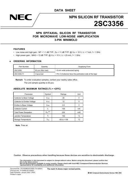
DATA SHEETNPN SILICON RF TRANSISTOR<strong>2SC3356</strong>NPN EPITAXIAL SILICON RF TRANSISTORFOR MICROWAVE LOW-NOISE AMPLIFICATION3-PIN MINIMOLDFEATURES• Low noise and high gain : NF = 1.1 dB TYP., Ga = 11 dB TYP. @ VCE = 10 V, IC = 7 mA, f = 1 GHz• High power gain : MAG = 13 dB TYP. @ VCE = 10 V, IC = 20 mA, f = 1 GHzORDERING INFORMATIONPart Number Quantity Supplying Form<strong>2SC3356</strong> 50 pcs (Non reel) • 8 mm wide embossed taping<strong>2SC3356</strong>-T1 3 kpcs/reel • Pin 3 (Collector) face the perforation side of the tapeRemark To order evaluation samples, contact your nearby sales office.The unit sample quantity is 50 pcs.ABSOLUTE MAXIMUM RATINGS (TA = +25°C)Parameter Symbol Ratings UnitCollector to Base Voltage VCBO 20 VCollector to Emitter Voltage VCEO 12 VEmitter to Base Voltage VEBO 3.0 VCollector Current IC 100 mATotal Power Dissipation Ptot Note 200 mWJunction Temperature Tj 150 °CStorage Temperature Tstg −65 to +150 °CNote Free airCaution Observe precautions when handling because these devices are sensitive to electrostatic discharge.The information in this document is subject to change without notice. Before using this document, please confirm thatthis is the latest version.Not all devices/types available in every country. Please check with local NEC Compound Semiconductor Devicesrepresentative for availability and additional information.Document No. PU10209EJ01V0<strong>DS</strong> (1st edition)(Previous No. P10356EJ5V1<strong>DS</strong>00)Date Published January 2003 CP(K)Printed in JapanThe markshows major revised points.© NEC Compound Semiconductor Devices 1985, 2003
<strong>2SC3356</strong>ELECTRICAL CHARACTERISTICS (TA = +25°C)Parameter Symbol Test Conditions MIN. TYP. MAX. UnitDC CharacteristicsCollector Cut-off Current ICBO VCB = 10 V, IE = 0 mA – – 1.0 µAEmitter Cut-off Current IEBO VEB = 1.0 V, IC = 0 mA – – 1.0 µADC Current Gain hFE Note 1 VCE = 10 V, IC = 20 mA 50 120 250 –RF CharacteristicsGain Bandwidth Product fT VCE = 10 V, IC = 20 mA – 7 – GHzInsertion Power Gain ⏐S21e⏐ 2 VCE = 10 V, IC = 20 mA, f = 1 GHz – 11.5 – dBNoise Figure NF VCE = 10 V, IC = 7 mA, f = 1 GHz – 1.1 2.0 dBReverse Transfer Capacitance Cre Note 2 VCB = 10 V, IE = 0 mA, f = 1 MHz − 0.55 1.0 pFNotes 1. Pulse measurement: PW ≤ 350 µs, Duty Cycle ≤ 2%2. Collector to base capacitance when the emitter groundedhFE CLASSIFICATIONRank R23/Q Note R24/R Note R25/S NoteMarking R23 R24 R25hFE Value 50 to 100 80 to 160 125 to 250Note Old Specification/New Specification2Data Sheet PU10209EJ01V0<strong>DS</strong>
<strong>2SC3356</strong>TYPICAL CHARACTERISTICS (TA = +25°C, unless otherwise specified)Total Power Dissipation Ptot (mW)25020015010050TOTAL POWER DISSIPATIONvs. AMBIENT TEMPERATURE0 25 50 75 100 125 150Ambient Temperature TA (˚C)Free airReverse Transfer Capacitance Cre (pF)REVERSE TRANSFER CAPACITANCEvs. COLLECTOR TO BASE VOLTAGE210.50.30.2 0.5 1 2 5 10 20 30Collector to Base Voltage VCB (V)f = 1 MHzDC Current Gain hFE2001005020DC CURRENT GAIN vs.COLLECTOR CURRENTVCE = 10 VGain Bandwidth Product fT (GHz)105210.50.2GAIN BANDWIDTH PRODUCTvs. COLLECTOR CURRENTVCE = 10 V100.5 1 5 10500.10.1 0.5 1 5 10 50 100Collector Current IC (mA)Collector Current IC (mA)INSERTION POWER GAIN, MAGvs. FREQUENCYINSERTION POWER GAINvs. COLLECTOR CURRENTInsertion Power Gain |S21e| 2 (dB)Maximum Available Power Gain MAG (dB)252015105|S21e| 2MAGVCE = 10 VIC = 20 mA00.05 0.1 0.2 0.5 1 2Insertion Power Gain |S21e| 2 (dB)15105VCE = 10 Vf = 1 GHz00.5 1 5 10 50 70Frequency f (GHz)Collector Current IC (mA)Data Sheet PU10209EJ01V0<strong>DS</strong> 3
<strong>2SC3356</strong>NOISE FIGURE vs.COLLECTOR CURRENTNOISE FIGURE, INSERTION POWER GAINvs. COLLECTOR TO EMITTER VOLTAGENoise Figure NF (dB)7654321VCE = 10 Vf = 1 GHzNoise Figure NF (dB)54321|S21e| 2NFf = 1 GHzIC = 20 mA1512963Insertion Power Gain |S21e| 2 (dB)00.5 1 5 10 50 70Collector Current IC (mA)Remark The graphs indicate nominal characteristics.002 4 6 8 10Collector to Emitter Voltage VCE (V)S-PARAMETERSS-parameters/Noise parameters are provided on the NEC Compound Semiconductor Devices Web site in a form(S2P) that enables direct import to a microwave circuit simulator without keyboard input.Click here to download S-parameters.[RF and Microwave] → [Device Parameters]URL http://www.csd-nec.com/4Data Sheet PU10209EJ01V0<strong>DS</strong>
0.441.00.130.371.62.00.31<strong>2SC3356</strong>SMITH CHARTS11e, S22e-FREQUENCYCONDITION : VCE = 10 V, 200 MHz Step0.020.010.490.480.030.480.490.47000.040.460.47WAVELENGTHS TOWARD GENERATOR0.010.020.03−160IN DEGREESANGLE OF REFLECTION COEFFCIENT0.100.10.051500.20.20.450.061400.30.10.440.070.40.43ZO )( +JX––––1300.080.42POSITIVE REACTANCE COMPONENT0.20.50.30.091200.60.410.7S11e0.40.100.401100.50.80.110.391002.0 GHz0.60.70.80.120.38REACTANCE COMPONENT( ––––R)ZO0.90.91.0900.130.370.20.20.40.41.20.21.20.140.36801.40.150.35700.160.34600.170.330.180.32500.2 GHz IC = 20 mA0.40.60.60.60.81.40.80.81.0IC = 20 mA1.01.61.01.01.82.01.61.83.02.04.05.0S22e0.31403.00.2 GHz100.190.200.304.030206.05.00.29201010IC = 5 mA205050200.21−200.220.28100−100.220.270.260.230.280.230.240.240.250.270.250.26WAVELENGTHS TOWARD LOAD0.460.04−1500.3NEGATIVE REACTANCE COMPONENT−300.290.450.05−1400.06ZO )––––( −JX0.60.80.2 GHz3.0−400.190.214.00.40.4IC = 5 mA0.200.300.5−1300.070.60.21.8−500.180.430.42−1200.70.41−1100.40−1000.390.38−90−800.36−700.350.34−600.320.080.090.100.80.110.90.121.01.20.141.40.150.160.330.17S21e-FREQUENCYCONDITION : VCE = 10 V, IC = 20 mAS12e-FREQUENCYCONDITION : VCE = 10 V, IC = 20 mA120˚90˚60˚120˚90˚2.0 GHz60˚0.2 GHz150˚S21e30˚150˚S12e30˚0.2 GHz180˚2.0 GHz5 10 15 200˚180˚0˚0.05 0.1 0.15 0.2 0.25–150˚–30˚–150˚–30˚–120˚–90˚–60˚–120˚–90˚–60˚Data Sheet PU10209EJ01V0<strong>DS</strong> 5
<strong>2SC3356</strong>PACKAGE DIMENSIONS3-PIN MINIMOLD (UNIT: mm)0.4 +0.1–0.052.8±0.21.50.65 +0.1–0.152.9±0.20.950.952130.4 +0.1–0.050.3Marking0 to 0.11.1 to 1.40.16 +0.1–0.05PIN CONNECTIONS1. Emitter2. Base3. Collector6Data Sheet PU10209EJ01V0<strong>DS</strong>
<strong>2SC3356</strong>• The information in this document is current as of January, 2003. The information is subject tochange without notice. For actual design-in, refer to the latest publications of NEC's data sheets ordata books, etc., for the most up-to-date specifications of NEC semiconductor products. Not allproducts and/or types are available in every country. Please check with an NEC sales representativefor availability and additional information.• No part of this document may be copied or reproduced in any form or by any means without priorwritten consent of NEC. NEC assumes no responsibility for any errors that may appear in this document.• NEC does not assume any liability for infringement of patents, copyrights or other intellectual property rights ofthird parties by or arising from the use of NEC semiconductor products listed in this document or any otherliability arising from the use of such products. No license, express, implied or otherwise, is granted under anypatents, copyrights or other intellectual property rights of NEC or others.• Descriptions of circuits, software and other related information in this document are provided for illustrativepurposes in semiconductor product operation and application examples. The incorporation of thesecircuits, software and information in the design of customer's equipment shall be done under the fullresponsibility of customer. NEC assumes no responsibility for any losses incurred by customers or thirdparties arising from the use of these circuits, software and information.• While NEC endeavours to enhance the quality, reliability and safety of NEC semiconductor products, customersagree and acknowledge that the possibility of defects thereof cannot be eliminated entirely. To minimizerisks of damage to property or injury (including death) to persons arising from defects in NECsemiconductor products, customers must incorporate sufficient safety measures in their design, such asredundancy, fire-containment, and anti-failure features.• NEC semiconductor products are classified into the following three quality grades:"Standard", "Special" and "Specific". The "Specific" quality grade applies only to semiconductor productsdeveloped based on a customer-designated "quality assurance program" for a specific application. Therecommended applications of a semiconductor product depend on its quality grade, as indicated below.Customers must check the quality grade of each semiconductor product before using it in a particularapplication."Standard": Computers, office equipment, communications equipment, test and measurement equipment, audioand visual equipment, home electronic appliances, machine tools, personal electronic equipmentand industrial robots"Special": Transportation equipment (automobiles, trains, ships, etc.), traffic control systems, anti-disastersystems, anti-crime systems, safety equipment and medical equipment (not specifically designedfor life support)"Specific": Aircraft, aerospace equipment, submersible repeaters, nuclear reactor control systems, lifesupport systems and medical equipment for life support, etc.The quality grade of NEC semiconductor products is "Standard" unless otherwise expressly specified in NEC'sdata sheets or data books, etc. If customers wish to use NEC semiconductor products in applications notintended by NEC, they must contact an NEC sales representative in advance to determine NEC's willingnessto support a given application.(Note)(1) "NEC" as used in this statement means NEC Corporation, NEC Compound Semiconductor Devices, Ltd.and also includes its majority-owned subsidiaries.(2) "NEC semiconductor products" means any semiconductor product developed or manufactured by or forNEC (as defined above).M8E 00. 4 - 0110Data Sheet PU10209EJ01V0<strong>DS</strong> 7
<strong>2SC3356</strong>Business issueNEC Compound Semiconductor Devices, Ltd.5th Sales Group, Sales Division TEL: +81-3-3798-6372 FAX: +81-3-3798-6783 E-mail: salesinfo@csd-nec.comNEC Compound Semiconductor Devices Hong Kong LimitedHong Kong Head OfficeTaipei Branch OfficeKorea Branch OfficeTEL: +852-3107-7303TEL: +886-2-8712-0478TEL: +82-2-528-0301FAX: +852-3107-7309FAX: +886-2-2545-3859FAX: +82-2-528-0302NEC Electronics (Europe) GmbH http://www.ee.nec.de/TEL: +49-211-6503-01 FAX: +49-211-6503-487California Eastern Laboratories, Inc. http://www.cel.com/TEL: +1-408-988-3500 FAX: +1-408-988-0279Technical issueNEC Compound Semiconductor Devices, Ltd. http://www.csd-nec.com/Sales Engineering Group, Sales DivisionE-mail: techinfo@csd-nec.com FAX: +81-44-435-19180209