K814P/ K824P/ K844P Optocoupler with Phototransistor ... - Rockby
K814P/ K824P/ K844P Optocoupler with Phototransistor ... - Rockby
K814P/ K824P/ K844P Optocoupler with Phototransistor ... - Rockby

You also want an ePaper? Increase the reach of your titles
YUMPU automatically turns print PDFs into web optimized ePapers that Google loves.
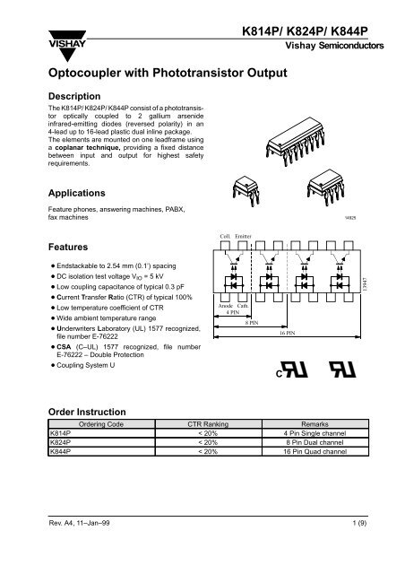
<strong>Optocoupler</strong> <strong>with</strong> <strong>Phototransistor</strong> OutputDescriptionThe <strong>K814P</strong>/ <strong>K824P</strong>/ <strong>K844P</strong> consist of a phototransistoroptically coupled to 2 gallium arsenideinfrared-emitting diodes (reversed polarity) in an4-lead up to 16-lead plastic dual inline package.The elements are mounted on one leadframe usinga coplanar technique, providing a fixed distancebetween input and output for highest safetyrequirements.<strong>K814P</strong>/ <strong>K824P</strong>/ <strong>K844P</strong>Vishay SemiconductorsApplicationsFeature phones, answering machines, PABX,fax machines14925FeaturesColl.Emitter Endstackable to 2.54 mm (0.1’) spacing DC isolation test voltage V IO = 5 kV Low coupling capacitance of typical 0.3 pF Current Transfer Ratio (CTR) of typical 100% Low temperature coefficient of CTR Wide ambient temperature range Underwriters Laboratory (UL) 1577 recognized,file number E-76222 CSA (C–UL) 1577 recognized, file numberE-76222 – Double Protection Coupling System UAnode Cath.4 PIN8 PINC16 PIN13947Order InstructionOrdering Code CTR Ranking Remarks<strong>K814P</strong> < 20% 4 Pin Single channel<strong>K824P</strong> < 20% 8 Pin Dual channel<strong>K844P</strong> < 20% 16 Pin Quad channelRev. A4, 11–Jan–99 1 (9)
<strong>K814P</strong>/ <strong>K824P</strong>/ <strong>K844P</strong>Vishay SemiconductorsAbsolute Maximum RatingsInput (Emitter)Parameter Test Conditions Symbol Value UnitReverse voltage V R 6 VForward current I F ±60 mAForward surge current t p ≤ 10 s I FSM ±1.5 APower dissipation T amb ≤ 25C P V 100 mWJunction temperature T j 125 COutput (Detector)Parameter Test Conditions Symbol Value UnitCollector emitter voltage V CEO 70 VEmitter collector voltage V ECO 7 VCollector current I C 50 mAPeak collector current t p /T = 0.5, t p ≤ 10 ms I CM 100 mAPower dissipation T amb ≤ 25C P V 150 mWJunction temperature T j 125 CCouplerParameter Test Conditions Symbol Value UnitAC Isolation test voltage (RMS) t = 1 min V 1) IO 5 kVTotal power dissipation T amb ≤ 25C P tot 250 mWOperating ambient temperatureT amb –40 to +100 CrangeStorage temperature range T stg –55 to +125 CSoldering temperature 2 mm from case, t ≤ 10 s T sd 260 C1) Related to standard climate 23/50 DIN 500142 (9)Rev. A4, 11–Jan–99
<strong>K814P</strong>/ <strong>K824P</strong>/ <strong>K844P</strong>Vishay SemiconductorsElectrical Characteristics (T amb = 25°C)Input (Emitter)Parameter Test Conditions Symbol Min. Typ. Max. UnitForward voltage I F = ±50 mA V F 1.25 1.6 VReverse current V R = ±6 V I R 10 AOutput (Detector)Parameter Test Conditions Symbol Min. Typ. Max. UnitCollector emitter voltage I C = 100 A V CEO 70 VEmitter collector voltage I E = 100 A V ECO 7 VCollector dark current V CE = 20 V, I F = 0, E = 0 I CEO 100 nACouplerParameter Test Conditions Symbol Min. Typ. Max. UnitCollector emitter I F = ± 10 mA, I C = 1 mA V CEsat 0.3 Vsaturation voltageCut-off frequency I F = ± 10 mA, V CE = 5 V, f c 100 kHzR L = 100 Coupling capacitance f = 1 MHz C k 0.3 pFCurrent Transfer Ratio (CTR)Parameter Test Conditions Type Symbol Min. Typ. Max. UnitI C /I F V CE = 5 V, I F = ± 5 mA CTR 0.2 3.0Rev. A4, 11–Jan–99 3 (9)
<strong>K814P</strong>/ <strong>K824P</strong>/ <strong>K844P</strong>Vishay SemiconductorsSwitching CharacteristicsParameter Test Conditions Symbol Typ. UnitDelay time V S = 5 V, IC = 2 mA, RL = 100 (see figure 1) t d 3.0 sRise timet r 3.0 sFall time t f 4.7 sStorage time t s 0.3 sTurn-on time t on 6.0 sTurn-off time t off 5.0 sTurn-on time V S = 5 V, IF = 10 mA, RL = 1 k (see figure 2) t on 9.0 sTurn-off timet off 18.0 s0R G= 50I FI F+ 5 VI C= 2 mA ;adjusted throughinput amplitudet pt p= 50 sT = 0.011334350 100 Channel IChannel IIOscilloscopeR L> 1 MC L< 20 pFFigure 1. Test circuit, non-saturated operation100%90%96 11698I F0tt pI C0R G= 50 I FI F= 10 mA+ 5 VI C10%0t rtt pT = 0.01t p= 50 st dt ont s t ft off50 1 kChannel IChannel IIOscilloscopeR L> 1 MC L< 20 pFt pt dt rt on (= t d + t r )pulse durationdelay timerise timeturn-on timet st ft off (= t s + t f )storage timefall timeturn-off time13344Figure 2. Test circuit, saturated operationFigure 3. Switching times4 (9)Rev. A4, 11–Jan–99
<strong>K814P</strong>/ <strong>K824P</strong>/ <strong>K844P</strong>Vishay SemiconductorsTypical Characteristics (T amb = 25 C, unless otherwise specified)P tot – Total Power Dissipation ( mW )30025020015010096 1170050Coupled device<strong>Phototransistor</strong>IR-diode00 40 80 120T amb – Ambient Temperature ( °C )Figure 4. Total Power Dissipation vs.Ambient TemperatureI CEO – Collector Dark Current,<strong>with</strong> open Base ( nA )1000095 11026100010010V CE =20VI F =010 25 50 75T amb – Ambient Temperature ( °C )Figure 7. Collector Dark Current vs.Ambient Temperature100I F – Forward Current ( mA )1000.0100.010.01.0I C – Collector Current ( mA )1001010.1V CE =5V0.10 0.2 0.4 0.6 0.8 1.0 1.2 1.4 1.6 1.8 2.096 11862V F – Forward Voltage ( V )Figure 5. Forward Current vs. Forward Voltage95 110270.010.1 1 10I F – Forward Current ( mA )100Figure 8. Collector Current vs. Forward CurrentCTR rel – Relative Current Transfer Ratio95 110252.01.51.00.50–25 0 25 50V CE =5VI F =5mAT amb – Ambient Temperature ( °C )Figure 6. Relative Current Transfer Ratio vs.Ambient Temperature75I C – Collector Current ( mA )95 10985100101I F =50mA0.10.1 1 1020mA10mA5mA2mA1mAV CE – Collector Emitter Voltage ( V )100Figure 9. Collector Current vs. Collector Emitter VoltageRev. A4, 11–Jan–99 5 (9)
<strong>K814P</strong>/ <strong>K824P</strong>/ <strong>K844P</strong>Vishay SemiconductorsV CEsat – Collector Emitter Saturation Voltage ( V )95 110281.00.80.60.40.2CTR=50%01 1010%20%I C – Collector Current ( mA )100Figure 10. Collector Emitter Saturation Voltage vs.Collector Currentt on / t off – Turn on / Turn off Time ( s )5040302010Saturated OperationV S =5VR L =1k00 5 10 1595 11031I F – Forward Current ( mA )Figure 12. Turn on / off Time vs. Forward Currentt offt on20CTR – Current Transfer Ratio ( % )95 11029100010010V CE =5V10.1 1 10I F – Forward Current ( mA )100Figure 11. Current Transfer Ratio vs. Forward Currentt on / t off – Turn on / Turn off Time ( s )108642t ont offNon SaturatedOperationV S =5VR L =10000 2 4 695 11030I C – Collector Current ( mA )Figure 13. Turn on / off Time vs. Collector Current10Pin 1 IndicationType<strong>K814P</strong>820UTK6315083DateCode(YM)CouplingSystemIndicatorCompanyLogoFigure 14. Marking exampleProductionLocation6 (9)Rev. A4, 11–Jan–99
<strong>K814P</strong>/ <strong>K824P</strong>/ <strong>K844P</strong>Vishay SemiconductorsDimensions of <strong>K814P</strong> in mmweight:ca. 0.25 gcreepage distance: 6 mmair path: 6 mmafter mounting on PC board14789Dimensions of <strong>K824P</strong> in mmweight:ca. 0.55 gcreepage distance: 6 mmair path: 6 mmafter mounting on PC board14784Rev. A4, 11–Jan–99 7 (9)14784
<strong>K814P</strong>/ <strong>K824P</strong>/ <strong>K844P</strong>Vishay SemiconductorsDimensions of <strong>K844P</strong> in mmweight:ca. 1.0 gcreepage distance: 6 mmair path: 6 mmafter mounting on PC board147838 (9)Rev. A4, 11–Jan–99
Ozone Depleting Substances Policy Statement<strong>K814P</strong>/ <strong>K824P</strong>/ <strong>K844P</strong>Vishay SemiconductorsIt is the policy of Vishay Semiconductor GmbH to1. Meet all present and future national and international statutory requirements.2. Regularly and continuously improve the performance of our products, processes, distribution and operatingsystems <strong>with</strong> respect to their impact on the health and safety of our employees and the public, as well astheir impact on the environment.It is particular concern to control or eliminate releases of those substances into the atmosphere which are knownas ozone depleting substances (ODSs).The Montreal Protocol (1987) and its London Amendments (1990) intend to severely restrict the use of ODSs andforbid their use <strong>with</strong>in the next ten years. Various national and international initiatives are pressing for an earlier banon these substances.Vishay Semiconductor GmbH has been able to use its policy of continuous improvements to eliminate the useof ODSs listed in the following documents.1. Annex A, B and list of transitional substances of the Montreal Protocol and the London Amendments respectively2. Class I and II ozone depleting substances in the Clean Air Act Amendments of 1990 by the EnvironmentalProtection Agency (EPA) in the USA3. Council Decision 88/540/EEC and 91/690/EEC Annex A, B and C (transitional substances) respectively.Vishay Semiconductor GmbH can certify that our semiconductors are not manufactured <strong>with</strong> ozone depletingsubstances and do not contain such substances.We reserve the right to make changes to improve technical design and may do so <strong>with</strong>out further notice.Parameters can vary in different applications. All operating parameters must be validated for each customerapplication by the customer. Should the buyer use Vishay Semiconductors products for any unintended or unauthorizedapplication, the buyer shall indemnify Vishay Semiconductors against all claims, costs, damages, and expenses, arising outof, directly or indirectly, any claim of personal damage, injury or death associated <strong>with</strong> such unintended orunauthorized use.Vishay Semiconductor GmbH, P.O.B. 3535, D-74025 Heilbronn, GermanyTelephone: 49 (0)7131 67 2831, Fax number: 49 (0)7131 67 2423Rev. A4, 11–Jan–99 9 (9)