
You also want an ePaper? Increase the reach of your titles
YUMPU automatically turns print PDFs into web optimized ePapers that Google loves.
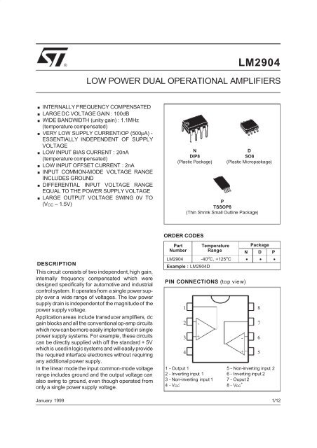
®<strong>LM2904</strong>LOW POWER DUAL OPERATIONAL AMPLIFIERS.INTERNALLY FREQUENCY COMPENSATEDLARGE DC VOLTAGE GAIN : 100dB.WIDE BANDWIDTH (unity gain) : 1.1MHz(temperature compensated)VERY LOW SUPPLY CURRENT/OP (500µA) -.ESSENTIALLY INDEPENDENT OF SUPPLYVOLTAGELOW INPUT BIAS CURRENT : 20nA.(temperature compensated)LOW INPUT OFFSET CURRENT : 2nA.INPUT COMMON-MODE VOLTAGE RANGEINCLUDES GROUND.DIFFERENTIAL INPUT VOLTAGE RANGEEQUAL TO THE POWER SUPPLY VOLTAGELARGE OUTPUT VOLTAGE SWING 0V TO(VCC –1.5V)NDIP8(Plastic Package)DSO8(Plastic Micropackage)PTSSOP8(Thin Shrink Small Outline Package)ORDER CODESDESCRIPTIONThis circuit consists of two independent,high gain,internally frequency compensated which weredesigned specifically for automotive and industrialcontrol system. It operatesfrom a single power supplyover a wide range of voltages. The low powersupply drain is independentof the magnitude of thepower supply voltage.Application areas include transducer amplifiers, dcgain blocks and all the conventionalop-amp circuitswhich nowcan bemore easily implementedin singlepower supply systems. For example, these circuitscan be directly supplied with off the standard + 5Vwhich is usedin logic systems and will easily providethe required interface electronics without requiringany additional power supply.In the linear mode the input common-mode voltagerange includes ground and the output voltage canalso swing to ground, even though operated fromonly a single power supply voltage.January 1999Part Temperature PackageNumber Range N D P<strong>LM2904</strong> -40 o C, +125 o C • • •Example : <strong>LM2904</strong>DPIN CONNECTIONS (top view)123-+ -4 + 51 - Output 15 - Non-inverting input 22 - Inverting input 16 - Inverting input 23 - Non-inverting input 1 7 - Ouput 24-VCC - 8-VCC +8761/12
<strong>LM2904</strong>ELECTRICAL CHARACTERISTICSVCC + = +5V, VCC – = Ground, VO = 1.4V, Tamb =25 o C (unless otherwise specified)Symbol Parameter Min. Typ. Max. UnitV io Input Offset Voltage - (note 3)Tamb =25 o CT min. ≤ T amb ≤ T max .2 79mVI ioInput Offset CurrentTamb =25 o CTmin. ≤ Tamb ≤ Tmax.Iib Input Bias Current - (note 4)T amb =25 o CT min. ≤ T amb ≤ T max .A vdSVRI CCVicmCMRIsourceIsinkV OPPLarge Signal Voltage Gain(V CC = +15V, R L =2kΩ,V O = 1.4V to 11.4V)Tamb =25 o CTmin. ≤ Tamb ≤ Tmax.Supply Voltage Rejection Ratio (RS = 10kΩ)(VCC + = 5 to 30V)T amb =25 o CT min. ≤ T amb ≤ T max .Supply Current, all Amp, no LoadV CC = +5V, T min. ≤ T amb ≤ T max .VCC = +30V, Tmin. ≤ Tamb ≤ Tmax.Input Common Mode Voltage Range(VCC = +30V) - (note 6)T amb =25 o CT min . ≤ T amb ≤ T max .Common-mode Rejection Ratio (RS = 10kΩ)T amb =25 o CT min. ≤ T amb ≤ T max .502565650070602 304020 1502001001000.7 1.2285V CC + –1.5V CC + –2Output Source Current(VCC = +15V, Vo = 2V, Vid = +1V) 20 40 60Output Current Sink (Vid = -1V)V CC = +15V, V O =2VV CC = +15V, V O = +0.2VOutput Voltage Swing (R L =2kΩ)T amb =25 o CT min. ≤ T amb ≤ T max .VOH High Level Output Voltage (VCC + = 30V)Tamb =25 o CRL =2kΩTmin. ≤ Tamb ≤ Tmax.T amb =25 o CR L = 10kΩTmin. ≤ Tamb ≤ Tmax.V OLSRGBPTHD1012002050V CC + –1.5V CC + –2Low Level Output Voltage (R L = 10kΩ)T amb =25 o C5 20T min . ≤ T amb ≤ T max. 20Slew Rate (VCC = 15V, VI = 0.5 to 3V, RL =2kΩ,CL=100pF, unity gain) 0.3 0.6Gain Bandwidth Product(V CC = 30V, f = 100kHz,V in = 10mV, R L =2kΩ,C L = 100pF) 0.7 1.1Total Harmonic Distortion(f = 1kHz, Av = 20dB, RL =2kΩ,VCC = 30V,0.02CL = 100pF, VO =2PP)262627272728nAnAV/mVdBmAVdBmAmAµAVVmVV/µsMHz%3/12
<strong>LM2904</strong>ELECTRICAL CHARACTERISTICS (continued)Symbol Parameter Min. Typ. Max UnitDVio Input Offset Voltage Drift 7 30 µA/ o CDI io Input Offset Current Drift 10 300 pA/ o CVO1/VO2 Channel Separation (note 5)1kHz ≤ f ≤ 20kHz 120dBNotes : 1. This input current only exist when the voltage at any of the input leads is driven negative. It is due to the collector-basejunction of the input PNP transistor becoming forward biased and thereby acting as input diode clamps.In addition to this diode action, there is also NPN parasitic action on the IC chip. This transistor action can causethe output voltages of the Op-amps to go to the V CC voltage level (or to ground for a large overdrive) for the timeduration that an input is driven negative.This is not destructive and normal output will set up again for input voltage higher than –0.3V.2. Short-circuits from the output to V CC can cause excessive heating if V + CC > 15V. The maximum output current isapproximatively 40mA independent of the magnitude of V CC. Destructive dissipation can result from simultaneousshort-circuits on all amplifiers.3. V O = 1.4V, R S =0Ω,5V
<strong>LM2904</strong>OUTPUT VOLTAGE (mV)INPUT CURRENT (mA)VOLTAGE FOLLOWER PULSSE RESPONSE(SMALL SIGNAL)500450400350300el+-OutputeO50pFInp utTamb =+25 CVCC =30V2500 1 2 3 4 5 6 7 8908070605040302010TIME (µs)INPUT CURRENT (Note 1)VCC =+30VV CC =+15VVCC =+5VVI =0VOUTPUT VOLTAGE REFERENCEDTO V CC+ (V)OUTPUT CURRENT (mA)9080706050403020108765OUTPUT CHARACTERISTICSV CCV CC /2 +V O-I O4Independent ofV CC3Tamb =+25 C210,001 0,01 0,1 1 10 100OUTPUT SOURCE CURRENT (mA)CURRENT LIMITING (Note 1)-I O+0-55 -35 -15 5 25 45 65 85 105 125TEMPERATURE ( C)INPUT VOLTAGE RANGE150-55 -35 -15 5 25 45 65 85 105 125TEMPERATURE ( C)SUPPLY CURRENT4V CCINPUT VOLTAGE (V)105NØgativePositiveSUPPLY CURRENT (mA)321mA-+I DT amb = 0 C to +125 CTamb =-55 C0 5 10 15POWER SUPPLY VOLTAGE (–V)0 10 20 30POSITIVE SUPPLY VOLTAGE (V)5/12
<strong>LM2904</strong>VOLTAGE GAIN (dB)1601208040RRLL= 20k Ω= 2k ΩINPUT CURRENT (nA)100755025T = +25 CambVOLTAGE GAIN (dB)0 10 20 30 40POSITIVE SUPP LY VOLTAGE (V)160R = 20k Ω12080R400 10 20 30POSITIVE S UPPLY VOLTAGE (V)LL= 2k ΩGAIN BANDWIDTH PRODUCT (MHz)1.51.351.21.050.90.750.60.450.30.150 10 20 30POSITIVE S UPPLY VOLTAGE (V)V = 15VCC0-55-35-15 5 25 45 65 85 105 125TEMPERATURE ( C)POWER SUPPLY REJECTION RATIO (dB)1151101051009590858075SVR7070656560-55-35-15 5 25 45 65 85 105 12560-55-35-15 5 25 45 65 85 105 125TEMPERATURE ( C)TEMPERATURE ( C)COMMON MODE REJECTION RATIO (dB)11511010510095908580756/12
<strong>LM2904</strong>TYPICAL APPLICATIONS (single supply voltage) VCC =+5VDCAC COUPLED INVERTING AMPLIFIERAC COUPLED NON-INVERTING AMPLIFIERC IR110kΩe I ~ R2V CC100kΩR100kΩf1/2<strong>LM2904</strong>R6.2kΩBR3100kΩA = - R fVR1(as shown A V = -10)C oe0 oR10kΩ L2V PPR1 R2100kΩ 1MΩA = 1 + R2V R1(as shown A V = 11)C o1/2C LM290 4e0IoRR6.2kΩB10kΩ LR3e I ~ 1MΩV CCC10.1µFR4100kΩ2V PPC110µFC210µFR5100kΩNON-INVERTING DC AMPLIFIERDC SUMMING AMPLIFIERe 1100kΩ10kΩ1/2<strong>LM2904</strong>e O +5VA V =1+ R2R1(As shown A V = 101)100kΩ1/2<strong>LM2904</strong>e Oe 2100kΩR110kΩR21MΩe O (V)e 3100kΩ0e I (mV)100kΩe 4100kΩeo =e1+e2-e3-e4where (e1 +e2)≥ (e3 +e4)to keep eo ≥ 0V7/12
<strong>LM2904</strong>HIGH INPUT Z, DC DIFFERENTIALAMPLIFIERUSING SYMMETRICAL AMPLIFIERS TOREDUCE INPUT CURRENTR1100kΩR2100kΩR3100kΩR4100kΩ1/2<strong>LM2904</strong>1/2+V1 <strong>LM2904</strong> V o+V2if R1 =R5and R3 =R4=R6=R7e o =[1+ 2R 1R 2] (e 2 − e 1 )As shown eo =101(e2-e1).e IIBI B1.5MΩI II B2N 9291/2<strong>LM2904</strong>0.001µFI B3MΩI B1/2<strong>LM2904</strong>e oInput current compensationHIGH INPUT Z ADJUSTABLE GAIN DCINSTRUMENTATION AMPLIFIERLOW DRIFT PEAK DETECTORR1100kΩI BR22kΩ1/2<strong>LM2904</strong>Gain adjustR5100kΩR3100kΩR4100kΩ1/2<strong>LM2904</strong>e Oe IZ I1/2<strong>LM2904</strong>1µF2I BCI B2I B2N 9291/2<strong>LM2904</strong>0.001µFI BZ oe oe 2e 11/2<strong>LM2904</strong>R6100kΩR7100kΩR1MΩ3R3MΩI B1/2<strong>LM2904</strong>Input curre ntcompens ationif R 1 =R 5 and R 3 =R 4 =R 6 = R 7e o = [1+ 2R 1] (e 2 − e 1 )R2As shown eo =101(e2-e1)8/12
<strong>LM2904</strong>ACTIVE BAND-PASS FILTERR1100kΩ+V1R2100kΩR3100kΩ1/2<strong>LM2904</strong>R410MΩC2330pF1/2<strong>LM2904</strong>R6470kΩC1330pF1/2<strong>LM2904</strong>R5470kΩR7100kΩVoF o = 1kHzQ=50A V = 100 (40dB)R8100kΩC310µFV CC9/12
<strong>LM2904</strong>PACKAGE MECHANICAL DATA8 PINS - PLASTIC DIPPM-DIP8.EPSDimensionsMillimetersInchesMin. Typ. Max. Min. Typ. Max.A 3.32 0.131a1 0.51 0.020B 1.15 1.65 0.045 0.065b 0.356 0.55 0.014 0.022b1 0.204 0.304 0.008 0.012D 10.92 0.430E 7.95 9.75 0.313 0.384e 2.54 0.100e3 7.62 0.300e4 7.62 0.300F 6.6 0260i 5.08 0.200L 3.18 3.81 0.125 0.150Z 1.52 0.060DIP8.TBL10/12
<strong>LM2904</strong>PACKAGE MECHANICAL DATA8 PINS - PLASTIC MICROPACKAGE (SO)PM-SO8.EPSDimensionsMillimetersInchesMin. Typ. Max. Min. Typ. Max.A 1.75 0.069a1 0.1 0.25 0.004 0.010a2 1.65 0.065a3 0.65 0.85 0.026 0.033b 0.35 0.48 0.014 0.019b1 0.19 0.25 0.007 0.010C 0.25 0.5 0.010 0.020c145 o (typ.)D 4.8 5.0 0.189 0.197E 5.8 6.2 0.228 0.244e 1.27 0.050e3 3.81 0.150F 3.8 4.0 0.150 0.157L 0.4 1.27 0.016 0.050M 0.6 0.024S8 o (max.)SO8.TBL11/12
<strong>LM2904</strong>PACKAGE MECHANICAL DATA8 PINS - THIN SHRINK SMALL OUTLINE PACKAGEPREVIEWDim.MillimetersInchesMin. Typ. Max. Min. Typ. Max.A 1.20 0.05A1 0.05 0.15 0.01 0.006A2 0.80 1.00 1.05 0.031 0.039 0.041b 0.19 0.30 0.007 0.15c 0.09 0.20 0.003 0.012D 2.90 3.00 3.10 0.114 0.118 0.122E 6.40 0.252E1 4.30 4.40 4.50 0.169 0.173 0.177e 0.65 0.025k 0 o 8 o 0 o 8 ol 0.50 0.60 0.75 0.09 0.0236 0.030Information furnished is believed to be accurate and reliable. However, STMicroelectronics assumes no responsibility for theconsequences of use of such information nor for any infringement of patents or other rights of third parties which may resultfrom its use. No license is granted by implication or otherwise under any patent or patent rights of STMicroelectronics. Specificationsmentioned in this publication are subject to change without notice. This publication supersedes and replaces all informationpreviously supplied. STMicroelectronics products are not authorized for use as critical components in life support devicesor systems without express written approval of STMicroelectronics.© The ST logo is a trademark of STMicroelectronics© 1999 STMicroelectronics – Printed in Italy – All Rights ReservedSTMicroelectronics GROUP OF COMPANIESAustralia - Brazil - Canada - China - France - Germany - Italy - Japan - Korea - Malaysia - Malta - Mexico - MoroccoThe Netherlands - Singapore - Spain - Sweden - Switzerland - Taiwan - Thailand - United Kingdo m - U.S.A.ORDER CODE :12/12
This datasheet has been download from:www.datasheetcatalog.com<strong>Datasheet</strong>s for electronics components.