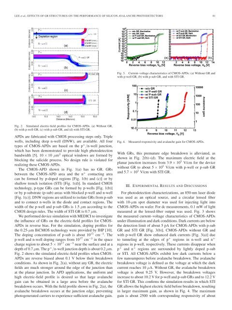
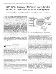
LEE et al.: EFFECTS OF GR STRUCTURES ON THE PERFORMANCE OF SILICON AVALANCHE PHOTODETECTORS 81Fig. 3. Current–voltage characteristics <str<strong>on</strong>g>of</str<strong>on</strong>g> CMOS-APDs: (a) Without GR andwith p-well GR, (b) with p-sub GR, and with STI GR.Fig. 2. Simulated electric-field pr<str<strong>on</strong>g>of</str<strong>on</strong>g>iles for CMOS-APDs. (a) Without GR,(b) with p-well GR, (c) with p-sub GR, and (d) with STI GR.APDs are fabricated with CMOS processing steps <strong>on</strong>ly. Triplewells, including deep n-well (DNW), are available. All fourtypes <str<strong>on</strong>g>of</str<strong>on</strong>g> CMOS-APDs are based <strong>on</strong> <strong>the</strong> p + /n-well juncti<strong>on</strong>,which has been dem<strong>on</strong>strated to provide high photodetecti<strong>on</strong>bandwidth [5]. 10 × 10 μm 2 optical windows are formed byblocking <strong>the</strong> salicide process. No design rule is violated forrealizing <strong>the</strong>se CMOS-APDs.The CMOS-APD shown in Fig. 1(a) has no GR. GRsbetween <strong>the</strong> CMOS-APD area and <strong>the</strong> n + c<strong>on</strong>tacting areacan be formed by p-doped regi<strong>on</strong>s [Fig. 1(b) and (c)] or byshallow trench isolati<strong>on</strong> (STI) [Fig. 1(d)]. In standard CMOStechnology, p-type GRs can be formed by p-wells [Fig. 1(b)]or by p-substrate (p-sub) areas with blocked p-well and n-well[Fig. 1(c)]. DNW regi<strong>on</strong>s are utilized to isolate GRs from p-suband to c<strong>on</strong>nect n-wells in <strong>the</strong> diode and c<strong>on</strong>tact regi<strong>on</strong>s. Thewidth <str<strong>on</strong>g>of</str<strong>on</strong>g> <strong>the</strong> p-well and p-sub GRs is 1.5 μm according to <strong>the</strong>CMOS design rules. The width <str<strong>on</strong>g>of</str<strong>on</strong>g> STI GR is 0.7 μm.We performed device simulati<strong>on</strong> with MEDICI to investigate<strong>the</strong> influence <str<strong>on</strong>g>of</str<strong>on</strong>g> GRs <strong>on</strong> <strong>the</strong> electric-field pr<str<strong>on</strong>g>of</str<strong>on</strong>g>iles for CMOS-APDs in reverse bias. For <strong>the</strong> simulati<strong>on</strong>, doping pr<str<strong>on</strong>g>of</str<strong>on</strong>g>iles for<strong>the</strong> 0.25-μm BiCMOS technology were provided by IHP [10].The doping c<strong>on</strong>centrati<strong>on</strong> <str<strong>on</strong>g>of</str<strong>on</strong>g> p-sub is about 10 15 cm −3 .Thep-well and n-well doping ranges from 10 17 cm −3 in <strong>the</strong> spacecharge regi<strong>on</strong> to about 5 × 10 17 cm −3 near <strong>the</strong> surface and at adepth <str<strong>on</strong>g>of</str<strong>on</strong>g> 0.7 μm. The p + /n-well juncti<strong>on</strong> depth is about 0.2 μm.Fig. 2 shows <strong>the</strong> simulated electric-field pr<str<strong>on</strong>g>of</str<strong>on</strong>g>iles when CMOS-APDs are reverse biased about 0.1 V below <strong>the</strong>ir breakdownc<strong>on</strong>diti<strong>on</strong>s. As shown in Fig. 2(a), without any GR, <strong>the</strong> electricfields are much str<strong>on</strong>ger around <strong>the</strong> edge <str<strong>on</strong>g>of</str<strong>on</strong>g> <strong>the</strong> juncti<strong>on</strong> thanat <strong>the</strong> planar juncti<strong>on</strong>. In APD applicati<strong>on</strong>s, <strong>the</strong> uniform andhigh electric-field pr<str<strong>on</strong>g>of</str<strong>on</strong>g>ile is desired so that large avalanchegain can be obtained in a large area before <strong>the</strong> avalanchebreakdown occurs. With <strong>the</strong> field pr<str<strong>on</strong>g>of</str<strong>on</strong>g>ile shown in Fig. 2(a), <strong>the</strong>avalanche breakdown occurs at <strong>the</strong> juncti<strong>on</strong> edge, preventingphotogenerated carriers to experience sufficient avalanche gain.Fig. 4.Measured resp<strong>on</strong>sivity and avalanche gain for CMOS-APDs.With GRs, this premature edge breakdown is alleviated, asshown in Fig. 2(b)–(d). The maximum electric field at <strong>the</strong>planar juncti<strong>on</strong> increases from 3.9 × 10 5 V/cm for <strong>the</strong> devicewithout GR to about 5 × 10 5 V/cm with p-well or p-sub GRand 5.7 × 10 5 V/cm with STI GR.III. EXPERIMENTAL RESULTS AND DISCUSSIONSFor photodetecti<strong>on</strong> characterizati<strong>on</strong>s, an 850-nm laser diodewas used as an optical source, and a circular lensed fiberwith 10-μm spot diameter was used for injecting light intoCMOS-APDs <strong>on</strong> wafer. For dc measurements, 0.1 mW <str<strong>on</strong>g>of</str<strong>on</strong>g> lightmeasured at <strong>the</strong> lensed-fiber output was used. Fig. 3 shows<strong>the</strong> measured current–voltage characteristics <str<strong>on</strong>g>of</str<strong>on</strong>g> CMOS-APDsunder illuminati<strong>on</strong> and dark c<strong>on</strong>diti<strong>on</strong>s. Dark currents are below<strong>the</strong> detecti<strong>on</strong> limit <str<strong>on</strong>g>of</str<strong>on</strong>g> about 5 pA for CMOS-APDs with p-subGR and STI GR [Fig. 3(b)]. CMOS-APDs without GR andwith p-well GR show enhanced dark currents [Fig. 3(a)] dueto tunneling at <strong>the</strong> edges <str<strong>on</strong>g>of</str<strong>on</strong>g> p + regi<strong>on</strong>s in n-well and n +regi<strong>on</strong>s in p-well, respectively. These currents disappear whenp + and n + regi<strong>on</strong>s are surrounded by lightly doped p-subor STI. All CMOS-APDs exhibit low dark currents below afew nanoamperes before avalanche breakdown. The avalanchebreakdown voltage is defined as <strong>the</strong> voltage at which <strong>the</strong> darkcurrent reaches 10 μA. Without GR, <strong>the</strong> avalanche breakdownvoltage is about 9.25 V. However, <strong>the</strong> breakdown voltagesincrease to about 10.2 V for p-well and p-sub GRs and to 12.2 Vfor STI GR. This c<strong>on</strong>firms <strong>the</strong> simulati<strong>on</strong> results in which STIGR allows <strong>the</strong> highest electric field before breakdown, resultingin larger maximum gain, as shown in Fig. 4. The maximumgain is about 2500 with corresp<strong>on</strong>ding resp<strong>on</strong>sivity <str<strong>on</strong>g>of</str<strong>on</strong>g> about
82 <strong>IEEE</strong> ELECTRON DEVICE LETTERS, VOL. 33, NO. 1, JANUARY 2012through <strong>the</strong> lensed fiber and most photogenerated carriers aregenerated in <strong>the</strong> planar juncti<strong>on</strong> regi<strong>on</strong>. Here, we normalizedM to its respective values for <strong>the</strong> CMOS-APDs without GR inorder to cancel out uncertainties due to <strong>the</strong> used approximateexpressi<strong>on</strong> for M. The obtained results agree well with <strong>the</strong>measurement results, as shown in Table I. The results showthat different GR structures produce different electric-fieldmagnitudes that <strong>the</strong> photogenerated carriers experience, which,in turn, influence <strong>the</strong> achievable avalanche gain. Clearly, STIprovides <strong>the</strong> optimum GR structure with <strong>the</strong> largest avalanchegain in standard CMOS technology.Fig. 5.Measured photodetecti<strong>on</strong> frequency resp<strong>on</strong>ses <str<strong>on</strong>g>of</str<strong>on</strong>g> CMOS-APDs.TABLE IAVALANCHE GAIN: CALCULATION AND MEASUREMENTIV. CONCLUSIONWe have investigated <strong>the</strong> effects <str<strong>on</strong>g>of</str<strong>on</strong>g> GR structures <strong>on</strong> <strong>the</strong> performance<str<strong>on</strong>g>of</str<strong>on</strong>g> CMOS-APDs. Four types <str<strong>on</strong>g>of</str<strong>on</strong>g> CMOS-APDs based<strong>on</strong> <strong>the</strong> p + /n-well juncti<strong>on</strong> with different GR structures realizedin standard CMOS technology are compared and analyzed. Itis dem<strong>on</strong>strated that <strong>the</strong> device with STI GR can provide <strong>the</strong>largest electric field at <strong>the</strong> planar juncti<strong>on</strong> and c<strong>on</strong>sequentlyprovides <strong>the</strong> maximum avalanche gain.ACKNOWLEDGMENT15.4 A/W for <strong>the</strong> device with STI GR, while it is about 300with about 1.9-A/W resp<strong>on</strong>sivity for <strong>the</strong> device without GR.Fig. 5 shows <strong>the</strong> normalized photodetecti<strong>on</strong> frequency resp<strong>on</strong>ses<str<strong>on</strong>g>of</str<strong>on</strong>g> CMOS-APDs at <strong>the</strong> bias voltage <str<strong>on</strong>g>of</str<strong>on</strong>g> about 0.1 Vbelow breakdown. For this measurement, an electro-opticalmodulator and a vector network analyzer were used with priorcalibrati<strong>on</strong> <str<strong>on</strong>g>of</str<strong>on</strong>g> cables and RF adaptors. The average opticalpower injected into photodetectors was 1 mW, and <strong>the</strong> measuredfrequency range was from 50 MHz to 13.5 GHz. Asshown in our previous works, slight peaking in <strong>the</strong> resp<strong>on</strong>seis observed because <str<strong>on</strong>g>of</str<strong>on</strong>g> <strong>the</strong> inductive comp<strong>on</strong>ent produced in<strong>the</strong> avalanche regime [5], [11]. The photodetecti<strong>on</strong> bandwidthsfor all CMOS-APDs are similar because all four devices arebased <strong>on</strong> <strong>the</strong> same juncti<strong>on</strong> structure. CMOS-APDs with p-welland p-sub GR structures have no appreciable difference in <strong>the</strong>photodetecti<strong>on</strong> frequency resp<strong>on</strong>se and have about 10 dB higherresp<strong>on</strong>se than <strong>the</strong> <strong>on</strong>e without GR. The CMOS-APD with STIGR has about 18 dB higher resp<strong>on</strong>se than <strong>the</strong> device withoutGR structures.The avalanche gain M in an APD can be roughly estimatedusing M =[1 − (1/2) · W · α eff (E M )] −1 [12], whereW is <strong>the</strong> depleti<strong>on</strong> width, E M is <strong>the</strong> maximum electric field,and α eff (E M ) is <strong>the</strong> effective i<strong>on</strong>izati<strong>on</strong> rate at <strong>the</strong> maximumelectric field. Using <strong>the</strong> aforementi<strong>on</strong>ed equati<strong>on</strong> with W andE M determined from <strong>the</strong> simulati<strong>on</strong> and α eff (E M ) from [9],<strong>the</strong> ratio <str<strong>on</strong>g>of</str<strong>on</strong>g> M between different types <str<strong>on</strong>g>of</str<strong>on</strong>g> CMOS-APDs can beestimated at <strong>the</strong> bias voltage <str<strong>on</strong>g>of</str<strong>on</strong>g> about 0.1 V below breakdown,as shown in Table I. For <strong>the</strong> structure without GR, <strong>the</strong> simulatedvalue <str<strong>on</strong>g>of</str<strong>on</strong>g> E M at <strong>the</strong> planar juncti<strong>on</strong> regi<strong>on</strong> is used for thisestimati<strong>on</strong> ra<strong>the</strong>r than at <strong>the</strong> corner <str<strong>on</strong>g>of</str<strong>on</strong>g> p + implantati<strong>on</strong> where<strong>the</strong> electric field is higher. This is because <strong>the</strong> corner regi<strong>on</strong> islocated outside <strong>the</strong> focused beam spot when light is injectedThe authors would like to thank IDEC for <strong>the</strong> EDA s<str<strong>on</strong>g>of</str<strong>on</strong>g>twaresupport.REFERENCES[1] T. K. Woodward and A. V. Krishnamoorthy, “1-Gb/s integrated opticaldetectors and receivers in commercial CMOS technologies,” <strong>IEEE</strong> J. Sel.Topics Quantum Electr<strong>on</strong>., vol. 5, no. 2, pp. 146–156, Mar.–Apr. 1999.[2] Intel Corp., Light Peak: Overview, San Jose, CA, 2010. [Online]. Available:http://www.intel.com/go/lightpeak[3] T. E. Sale, C. Chu, J.-K. Hwang, G.-H. Koh, R. Nabiev, J. L. Tan,L. M. Giovane, and M. V. R. Murty, “Manufacturability <str<strong>on</strong>g>of</str<strong>on</strong>g> 850 nm datacommunicati<strong>on</strong> VCSELs in high volume,” in Proc. Vertical-Cavity Surf.-Emitting Lasers XIV, Feb. 2010, vol. 7615, pp. 761 503-1–761 503-10.[4] N. Izhaky, M. T. Morse, S. Koehl, O. Cohen, D. Rubin, A. Barkai,G. Sarid, R. Cohen, and M. J. Paniccia, “Development <str<strong>on</strong>g>of</str<strong>on</strong>g> CMOScompatibleintegrated silic<strong>on</strong> phot<strong>on</strong>ics devices,” <strong>IEEE</strong> J. Sel. TopicsQuantum Electr<strong>on</strong>., vol. 12, no. 6, pp. 1688–1698, Nov.–Dec. 2006.[5] H.-S. Kang, M.-J. Lee, and W.-Y. Choi, “Si avalanche photodetectors fabricatedin standard complementary metal–oxide-semic<strong>on</strong>ductor process,”Appl. Phys. Lett., vol. 90, no. 15, pp. 151 118-1–151 118-3, Apr. 2007.[6] M.-J. Lee and W.-Y. Choi, “A silic<strong>on</strong> avalanche photodetector fabricatedwith standard CMOS technology with over 1 THz gain-bandwidth product,”Opt. Exp., vol. 18, no. 23, pp. 24 189–24 194, Nov. 2010.[7] C. Basavanagoud and K. N. Bhat, “Effect <str<strong>on</strong>g>of</str<strong>on</strong>g> lateral curvature <strong>on</strong> <strong>the</strong> breakdownvoltage <str<strong>on</strong>g>of</str<strong>on</strong>g> planar diodes,” <strong>IEEE</strong> Electr<strong>on</strong> Device Lett., vol.EDL-6,no. 6, pp. 276–278, Jun. 1985.[8] A. Rochas, A. R. Pauchard, P.-A. Besse, D. Pantic, Z. Prijic, andR. S. Popovic, “Low-noise silic<strong>on</strong> avalanche photodiodes fabricatedin c<strong>on</strong>venti<strong>on</strong>al CMOS technologies,” <strong>IEEE</strong> Trans. Electr<strong>on</strong> Devices,vol. 49, no. 3, pp. 387–394, Mar. 2002.[9]S.M.SzeandK.K.Ng,Physics <str<strong>on</strong>g>of</str<strong>on</strong>g> Semic<strong>on</strong>ductor Devices, 3rd ed.Hoboken, NJ: Wiley, 2007.[10] B. Heinemann, R. Barth, D. Knoll, H. Rücker, B. Tillack, andW. Winkler, “High-performance BiCMOS technologies withoutepitaxially-buried subcollectors and deep trenches,” Semic<strong>on</strong>d. Sci.Technol., vol. 22, no. 1, pp. 153–157, Jan. 2007.[11] M.-J. Lee, H.-S. Kang, and W.-Y. Choi, “Equivalent circuit model for Siavalanche photodetectors fabricated in standard CMOS process,” <strong>IEEE</strong>Electr<strong>on</strong> Device Lett., vol. 29, no. 10, pp. 1115–1117, Oct. 2008.[12] A. G. Chynoweth, “I<strong>on</strong>izati<strong>on</strong> rates for electr<strong>on</strong>s and holes in silic<strong>on</strong>,”Phys. Rev. Lett., vol. 109, no. 5, pp. 1357–1540, Mar. 1958.