2981 AND 2982 - users.757.org
2981 AND 2982 - users.757.org
2981 AND 2982 - users.757.org

You also want an ePaper? Increase the reach of your titles
YUMPU automatically turns print PDFs into web optimized ePapers that Google loves.
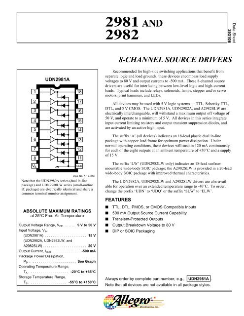
Data Sheet29310E<strong>2981</strong> <strong>AND</strong><strong>2982</strong>8-CHANNEL SOURCE DRIVERS12345678V SUDN<strong>2981</strong>A1817161514131211GNDDwg. No. A-10, 243Note that the UDN2980A series (dual in-linepackage) and UDN2980LW series (small-outlineIC package) are electrically identical and share acommon terminal number assignment.ABSOLUTE MAXIMUM RATINGSat 25°C Free-Air TemperatureOutput Voltage Range, V CE . . . . . . . . . 5 V to 50 VInput Voltage, V IN(UDN<strong>2981</strong>A) . . . . . . . . . . . . . . . . . . . . . . 15 V(UDN<strong>2982</strong>A, UDN<strong>2982</strong>LW, andA<strong>2982</strong>SLW) . . . . . . . . . . . . . . . . . . . . . . . 20 VOutput Current, I OUT . . . . . . . . . . . . . . -500 mAPackage Power Dissipation,P D . . . . . . . . . . . . . . . . . . . . . . . See GraphOperating Temperature Range,T A . . . . . . . . . . . . . . . . . . . . -20°C to +85°CStorage Temperature Range,T S . . . . . . . . . . . . . . . . . . . -55°C to +150°CRecommended for high-side switching applications that benefit fromseparate logic and load grounds, these devices encompass load supplyvoltages to 80 V and output currents to -500 mA. These 8-channel sourcedrivers are useful for interfacing between low-level logic and high-currentloads. Typical loads include relays, solenoids, lamps, stepper and/or servomotors, print hammers, and LEDs.All devices may be used with 5 V logic systems — TTL, Schottky TTL,DTL, and 5 V CMOS. The UDN<strong>2981</strong>A, UDN<strong>2982</strong>A, and A<strong>2982</strong>SLW areelectrically interchangeable, will withstand a maximum output off voltage of50 V, and operate to a minimum of 5 V. All devices in this series integrateinput current limiting resistors and output transient suppression diodes, andare activated by an active high input.The suffix ‘A’ (all devices) indicates an 18-lead plastic dual in-linepackage with copper lead frame for optimum power dissipation. Undernormal operating conditions, these devices will sustain 120 mA continuouslyfor each of the eight outputs at an ambient temperature of +50°C and a supplyof 15 V.The suffix ‘LW’ (UDN<strong>2982</strong>LW only) indicates an 18-lead surfacemountablewide-body SOIC package; the A<strong>2982</strong>SLW is provided in a 20-leadwide-body SOIC package with improved thermal characteristics.The UDN<strong>2982</strong>A, UDN<strong>2982</strong>LW and A<strong>2982</strong>SLW drivers are also availablefor operation over an extended temperature range to -40°C. To order,change the prefix ‘UDN’ to ‘UDQ’ or the suffix ‘SLW’ to ‘ELW’.FEATURES■■■■■TTL, DTL, PMOS, or CMOS Compatible Inputs500 mA Output Source Current CapabilityTransient-Protected OutputsOutput Breakdown Voltage to 80 VDIP or SOIC PackagingAlways order by complete part number, e.g., UDN<strong>2981</strong>A .Note that all devices are not available in all package styles.
<strong>2981</strong> <strong>AND</strong> <strong>2982</strong>8-CHANNELSOURCE DRIVERSOne of Eight DriversV 5920 K2983/84 ONLY7.2 KINPUT3 KOUTPUT1.5 KGROUNDDwg. No. A-10,242BA<strong>2982</strong>SLW2.5+V SNOCONNECTION12345678910NCNC20191817161514131211GROUNDNOCONNECTIONDwg. PP-064-2ALLOWABLE PACKAGE POWER DISSIPATION IN WATTS2.01.51.00.502518-PIN DIP, RθJA = 60°C/W20-LEAD SOIC, RθJA = 90°C/W18-LEAD SOIC, RθJA = 94°C/W50 75 100 125 150AMBIENT TEMPERATURE IN °CDwg. GP-022-4A2115 Northeast Cutoff, Box 15036Worcester, Massachusetts 01615-0036 (508) 853-5000Copyright © 1977, 2004 Allegro MicroSystems, Inc.
<strong>2981</strong> <strong>AND</strong> <strong>2982</strong>8-CHANNELSOURCE DRIVERSELECTRICAL CHARACTERISTICS at T A = +25°C (unless otherwise specified).Applicable Test LimitsCharacteristic Symbol Devices Test Conditions Fig. Min. Typ. Max. UnitsOutput Leakage Current I CEX All V IN = 0.4 V*, V S = 50 V, T A = +70°C 1 — — 200 µAOutput Sustaining V CE(SUS) All I OUT = -45 mA — 35 — — VVoltageCollector-Emitter V CE(SAT) All V IN = 2.4 V, I OUT = -100 mA 2 — 1.6 1.8 VSaturation Voltage V IN = 2.4 V, I OUT = -225 mA 2 — 1.7 1.9 VV IN = 2.4 V, I OUT = -350 mA 2 — 1.8 2.0 VInput Current I IN(ON) UDN<strong>2981</strong>A V IN = 2.4 V 3 — 140 200 µAV IN = 3.85 V 3 — 310 450 µA<strong>2982</strong>† V IN = 2.4 V 3 — 140 200 µAV IN = 12 V 3 — 1.25 1.93 mAOutput Source Current l OUT UDN<strong>2981</strong>A V IN = 2.4 V, V CE = 2.0 V 2 -350 — — mA(Outputs Open) <strong>2982</strong>† V IN = 2.4 V, V CE = 2.0 V 2 -350 — — mASupply Current I S All V IN = 2.4 V*, V S = 50 V 4 — — 10 mALeakage CurrentClamp Diode I R All V R = 50 V, V IN = 0.4 V* 5 — — 50 µAClamp Diode V F All I F = 350 mA 6 — 1.5 2.0 VTurn-On Delay t ON All 0.5 E IN to 0.5 E OUT , R L = 100Ω, — — 1.0 2.0 µsV S = 35 VTurn-Off Delay t OFF All 0.5 E IN to 0.5 E OUT , R L = 100Ω, — — 5.0 10 µsV S = 35 V, See NoteNOTES:Turn-off delay is influenced by load conditions. Systems applications well below the specified output loading may requiretiming considerations for some designs, i.e., multiplexed displays or when used in combination with sink drivers in a totempole configuration.Negative current is defined as coming out of (sourcing) the specified device terminal.* All inputs simultaneously.† Complete part number includes a prefix (A or UDN) and a suffix (A or SLW) as follows:UDN<strong>2981</strong>A, UDN<strong>2982</strong>A, UDN<strong>2982</strong>LW, or A<strong>2982</strong>SLW.www.allegromicro.com 3
<strong>2981</strong> <strong>AND</strong> <strong>2982</strong>8-CHANNELSOURCE DRIVERSTEST FIGURESFigure 1 Figure 2 Figure 3VSVSVSVVCEmAI INmAOPENV INµAI CEXVINI OUTV INDwg. No. A-11,083 Dwg. No. A-11,084 Dwg. No. A-11,085Figure 4Figure 5 Figure 6VSI SmAV INOPENV SI RV INµAOPENOPENV FVI FDwg. No. A-11,086 Dwg. No. A-11,087 Dwg. No. A-11,0884115 Northeast Cutoff, Box 15036Worcester, Massachusetts 01615-0036 (508) 853-5000
<strong>2981</strong> <strong>AND</strong> <strong>2982</strong>8-CHANNELSOURCE DRIVERSAllowable peak collector currentas a function of duty cycleSeries UDN2980A500500450450ALLOWABLE PEAK COLLECTOR CURRENT IN mA AT 50°C400350300250200150100RECOMMENDED MAXIMUM OUTPUT CURRENTV = 35 VSNUMBER OF OUTPUTSCONDUCTINGSIMULTANEOUSLY8 7 6543ALLOWABLE PEAK COLLECTOR CURRENT IN mA AT 70°C400350300250200150100RECOMMENDED MAXIMUM OUTPUT CURRENTV = 35 VSNUMBER OF OUTPUTSCONDUCTINGSIMULTANEOUSLY8 7 654350500010203040 50 60PER CENT DUTY CYCLE7080901000010203040 50 60PER CENT DUTY CYCLE708090100Dwg. No. A-11,106BDwg. No. A-11,111BUDN<strong>2981</strong>A and UDN<strong>2982</strong>A500500450450ALLOWABLE PEAK COLLECTOR CURRENT IN mA AT 50°C400350300250200150100RECOMMENDED MAXIMUM OUTPUT CURRENTV = 15 VSNUMBER OF OUTPUTSCONDUCTINGSIMULTANEOUSLY8 7 6543ALLOWABLE PEAK COLLECTOR CURRENT IN mA AT 70°C400350300250200150100RECOMMENDED MAXIMUM OUTPUT CURRENTNUMBER OF OUTPUTSCONDUCTINGSIMULTANEOUSLY8 7 65435050V = 15 VS0010203040 50 60PER CENT DUTY CYCLE7080 90 100Dwg. No. A-11,107B0010203040 50 60PER CENT DUTY CYCLE7080 90 100Dwg. No. A-11,108Bwww.allegromicro.com 5
<strong>2981</strong> <strong>AND</strong> <strong>2982</strong>8-CHANNELSOURCE DRIVERSAllowable peak collector currentas a function of duty cycleInput current as a functionof input voltageTypical electrosensitiveprinter application2.5ELECTRODES2.0IN 1118R LINPUT CURRENT, IIN(mA)1.51.00.5MAXIMUMTYPICALIN 2IN 3IN 4IN 5IN 6IN 7234567171615141312R LR LR LR LR LR L2 4 6 8 10 12INPUT VOLTAGE (VOLTS)IN 8V S891110R LDwg. No. A-11,115BDwg. No. A-11,113A6115 Northeast Cutoff, Box 15036Worcester, Massachusetts 01615-0036 (508) 853-5000
<strong>2981</strong> <strong>AND</strong> <strong>2982</strong>8-CHANNELSOURCE DRIVERS18UDN<strong>2981</strong>A and UDN<strong>2982</strong>ADimensions in Inches(controlling dimensions)100.0140.0080.2800.2400.430MAX0.300BSC10.0700.10090.0450.920BSC0.8800.005MIN0.210MAX0.015MIN0.1500.1150.0220.014Dwg. MA-001-18A in18Dimensions in Millimeters(for reference only)100.3550.2047.116.107.62BSC10.92MAX11.772.5491.1523.37BSC22.350.13MIN5.33MAX0.39MIN3.812.930.5580.356Dwg. MA-001-18A mmNOTES: 1. Exact body and lead configuration at vendor’s option within limits shown.2. Lead spacing tolerance is non-cumulative.3. Lead thickness is measured at seating plane or below.4. Supplied in standard sticks/tubes of 21 devices.www.allegromicro.com 7
<strong>2981</strong> <strong>AND</strong> <strong>2982</strong>8-CHANNELSOURCE DRIVERSUDN<strong>2982</strong>LW(add “TR” to part number for tape and reel)Dimensions in Inches(for reference only)18 100.01250.00910.29920.29140.4190.3940.0500.0160.0200.0131 2 30.46250.44690.050BSC0° TO 8°0.09260.10430.0040 MIN.Dwg. MA-008-18A in18Dimensions in Millimeters(controlling dimensions)100.320.237.607.4010.6510.001.270.400.510.3312 311.7511.351.27BSC0° TO 8°2.652.350.10 MIN.Dwg. MA-008-18A mmNOTES: 1. Exact body and lead configuration at vendor’s option within limits shown.2. Lead spacing tolerance is non-cumetive.3. Supplied in standard sticks/tubes of 41 devices or add “TR” to part number for tape and reel.8115 Northeast Cutoff, Box 15036Worcester, Massachusetts 01615-0036 (508) 853-5000
<strong>2981</strong> <strong>AND</strong> <strong>2982</strong>8-CHANNELSOURCE DRIVERSA<strong>2982</strong>SLW(add “TR” to part number for tape and reel)Dimensions in Inches(for reference only)20 110.01250.00910.29920.29140.4190.3940.0500.0160.0200.0131 2 30.51180.49610.050BSC0° TO 8°0.09260.10430.0040 MIN.Dwg. MA-008-20 in20Dimensions in Millimeters(controlling dimensions)110.320.237.607.4010.6510.001.270.400.510.3312 313.0012.601.27BSC0° TO 8°2.652.350.10 MIN.Dwg. MA-008-20 mmNOTES: 1. Exact body and lead configuration at vendor’s option within limits shown.2. Lead spacing tolerance is non-cumulative.3. Supplied in standard sticks/tubes of 37 devices or add “TR” to part number for tape and reel.www.allegromicro.com 9
<strong>2981</strong> <strong>AND</strong> <strong>2982</strong>8-CHANNELSOURCE DRIVERSThe products described here are manufactured under one or more U.S. patents or U.S.patents pending.Allegro MicroSystems, Inc. reserves the right to make, from time to time, such departuresfrom the detail specifications as may be required to permit improvements in the performance,reliability, or manufacturability of its products. Before placing an order, the user is cautionedto verify that the information being relied upon is current.Allegro products are not authorized for use as critical components in life-support devices orsystems without express written approval.The information included herein is believed to be accurate and reliable. However, AllegroMicroSystems, Inc. assumes no responsibility for its use; nor for any infringement of patents orother rights of third parties which may result from its use.10115 Northeast Cutoff, Box 15036Worcester, Massachusetts 01615-0036 (508) 853-5000