IXTA220N04T2 IXTP220N04T2 V
IXTA220N04T2 IXTP220N04T2 V
IXTA220N04T2 IXTP220N04T2 V

You also want an ePaper? Increase the reach of your titles
YUMPU automatically turns print PDFs into web optimized ePapers that Google loves.
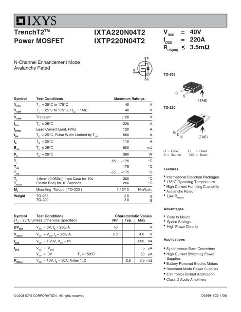
TrenchT2 TMPower MOSFET<strong>IXTA220N04T2</strong><strong>IXTP220N04T2</strong>V DSSI D25R DS(on)= 40V= 220A≤ 3.5mΩN-Channel Enhancement ModeAvalanche RatedTO-263Symbol Test Conditions Maximum RatingsV DSST J= 25°C to 175°C 40 VV DGRT J= 25°C to 175°C, R GS= 1MΩ 40 VTO-220GS(TAB)V GSMTransient ± 20 VI D25T C= 25°C 220 AI LRMSLead Current Limit, RMS 120 AI DMT C= 25°C, Pulse Width Limited by T JM660 AI AT C= 25°C 110 AE AST C= 25°C 600 mJP DT C= 25°C 360 WT J-55 ... +175 °CT JM175 °CT stg-55 ... +175 °CT L1.6mm (0.062in.) from Case for 10s 300 °CT SOLDPlastic Body for 10 Seconds 260 °CM dMounting Torque ( TO-220 ) 1.13/10 Nm/lb.in.Weight TO-263 2.5 gTO-220 3.0 gGDSG = Gate D = DrainS = Source TAB = DrainFeatures• International Standard Packages• 175°C Operating Temperature• High Current Handling Capability• Avalanche Rated• Low R DS(on)(TAB)AdvantagesSymbol Test Conditions Characteristic Values(T J= 25°C Unless Otherwise Specified) Min. Typ. Max.BV DSSV GS= 0V, I D= 250μA 40 VV GS(th)V DS= V GS, I D= 250μA 2.0 4.0 VI GSSV GS= ± 20V, V DS= 0V ±200 nAI DSSV DS= V DSS5 μAV GS= 0V T J= 150°C 50 μAR DS(on)V GS= 10V, I D= 50A, Notes 1, 2 2.8 3.5 mΩ• Easy to Mount• Space Savings• High Power DensityApplications• Synchronous Buck Converters• High Current Switching PowerSupplies• Battery Powered Electric Motors• Resonant-Mode Power Supplies• Electronics Ballast Application• Class D Audio Amplifiers© 2008 IXYS CORPORATION, All rights reservedDS99918C(11/08)
Symbol Test Conditions Characteristic Values(T J= 25°C, Unless Otherwise Specified) Min. Typ. Max.g fsV DS= 10V, I D= 60A, Note 1 40 66 SC iss6820 pFC ossV GS= 0V, V DS= 25V, f = 1MHz 1185 pFC rss250 pFt d(on)15 nsResistive Switching Timest r21 nsVt GS= 10V, V DS= 20V, I D= 50Ad(off)31 nsRt G= 3.3Ω (External)f21 nsQ g(on)112 nCQ gsV GS= 10V, V DS= 0.5 • V DSS, I D= 0.5 • I D2533 nCQ gd30 nCR thJC0.42 °C/WR thCHTO-220 0.50 °C/W<strong>IXTA220N04T2</strong><strong>IXTP220N04T2</strong>TO-263 (IXTA) OutlineSource-Drain DiodeSymbol Test Conditions Characteristic Values(T J= 25°C, Unless Otherwise Specified) Min. Typ. Max.I SV GS= 0V 220 AI SMRepetitive, Pulse Width Limited by T JM660 AV SDI F= 50A, V GS= 0V, Note 1 1.1 Vt rr I F= 110A, V GS= 0V45 nsI RM-di/dt = 100A/μs1.4 AQ RMV R= 20V32 nCTO-220 (IXTP) OutlineNotes: 1. Pulse Test, t ≤ 300μs; Duty Cycle, d ≤ 2%.2. On Through-Hole Packages, R DS(on)Kelvin Test ContactLocation must be 5mm or Less from the Package Body.Pins: 1 - Gate 2 - Drain3 - Source 4 - DrainIXYS reserves the right to change limits, test conditions, and dimensions.IXYS MOSFETs and IGBTs are covered 4,835,592 4,931,844 5,049,961 5,237,481 6,162,665 6,404,065 B1 6,683,344 6,727,585 7,005,734 B2 7,157,338B2by one or more of the following U.S. patents: 4,850,072 5,017,508 5,063,307 5,381,025 6,259,123 B1 6,534,343 6,710,405 B2 6,759,692 7,063,975 B24,881,106 5,034,796 5,187,117 5,486,715 6,306,728 B1 6,583,505 6,710,463 6,771,478 B2 7,071,537
<strong>IXTA220N04T2</strong><strong>IXTP220N04T2</strong>Fig. 1. Output Characteristics@ 25ºCFig. 2. Extended Output Characteristics@ 25ºC220200180160V GS = 15V10V9V8V350300250V GS = 15V10V9V8VID - Amperes14012010080607V6VID - Amperes2001501007V6V405V2000 0.1 0.2 0.3 0.4 0.5 0.6 0.7V DS - Volts505V00.0 0.5 1.0 1.5 2.0 2.5 3.0 3.5V DS - VoltsFig. 3. Output Characteristics@ 150ºCFig. 4. R DS(on) Normalized to I D = 110A Valuevs. Junction TemperatureID - Amperes2202001801601401201008060V GS = 15V10V9V8V7V6VRDS(on) - Normalized2.01.81.61.41.21.0V GS = 10VI D = 220AI D = 110A40205V0.800.0 0.2 0.4 0.6 0.8 1.0 1.2 1.4V DS - Volts0.6-50 -25 0 25 50 75 100 125 150 175T J - Degrees CentigradeRDS(on) - Normalized2.22.01.81.61.41.21.0Fig. 5. R DS(on) Normalized to I D = 110A Valuevs. Drain CurrentV GS = 10V15V - - - -0.80 40 80 120 160 200 240 280 320I D - AmperesT J = 175ºCT J = 25ºCID - AmperesFig. 6. Drain Current vs. Case Temperature130120110External Lead Current Limit1009080706050403020100-50 -25 0 25 50 75 100 125 150 175T C - Degrees Centigrade© 2008 IXYS CORPORATION, All rights reserved
<strong>IXTA220N04T2</strong><strong>IXTP220N04T2</strong>Fig. 7. Input AdmittanceFig. 8. Transconductance160120T J = - 40ºC140100ID - Amperes120100806040T J =150ºC25ºC- 40ºCg f s - Siemens80604025ºC150ºC202002.5 3 3.5 4 4.5 5 5.5 6 6.5V GS - Volts00 20 40 60 80 100 120 140 160I D - AmperesFig. 9. Forward Voltage Drop ofIntrinsic DiodeFig. 10. Gate Charge30027024021010987V DS = 20VI D = 110AI G = 10mAIS - Amperes180150120VGS - Volts65490T J = 150ºC360T J = 25ºC230100.3 0.4 0.5 0.6 0.7 0.8 0.9 1.0 1.1 1.2 1.3V SD - Volts00 20 40 60 80 100 120Q G - NanoCoulombsFig. 11. CapacitanceFig. 12. Forward-Bias Safe Operating Area100,0001,000f = 1 MHzR DS(on) LimitCapacitance - PicoFarads10,000C issC oss1,000C rss1000 5 10 15 20 25 30 35 40V DS - VoltsI D - Amperes10010External Lead LimitT J = 175ºCT C = 25ºCSingle Pulse11 10 100V DS - VoltsDC25µs100µs1ms10ms100msIXYS reserves the right to change limits, test conditions, and dimensions.IXYS REF: T_220N04T2(V5) 12-15-08-D
<strong>IXTA220N04T2</strong><strong>IXTP220N04T2</strong>t r - Nanoseconds282726252423222120191817Fig. 13. Resistive Turn-onRise Time vs. Junction TemperatureR G = 3.3ΩV GS = 10VV DS = 20VI D = 110AI D = 220A1625 35 45 55 65 75 85 95 105 115 125T J - Degrees CentigradeFig. 15. Resistive Turn-onSwitching Times vs. Gate Resistancet r - Nanoseconds28272625242322212019Fig. 14. Resistive Turn-onRise Time vs. Drain Current1840 60 80 100 120 140 160 180 200I D - AmperesT J = 125ºCT J = 25ºCR G = 3.3ΩV GS = 10VV DS = 20VFig. 16. Resistive Turn-offSwitching Times vs. Junction Temperaturet r - Nanoseconds1307012065t r t d(on) - - - -11060T J = 125ºC, V GS = 10V100V DS = 20V55905080457040603550I D = 220A, 110A304025302020151010052 4 6 8 10 12 14 16 18 20R G - Ohmst d(on)- Nanosecondst f - Nanoseconds3634 t f t d(off) - - - -424032 R G = 3.3Ω, V GS = 10V3830 V DS = 20V36283426I D = 220A322430222820I D = 110A 26182416221420121825 35 45 55 65 75 85 95 105 115 125T J - Degrees Centigradet d(off)- Nanosecondst f - Nanoseconds42383430262218Fig. 17. Resistive Turn-offSwitching Times vs. Drain CurrentT J = 25ºC142240 60 80 100 120 140 160 180 200I D - Amperest f t d(off) - - - -R G = 3.3Ω, V GS = 10VV DS = 20VT J = 125ºC50464238343026t d(off)- Nanosecondst f - Nanoseconds20018016014012010080604020Fig. 18. Resistive Turn-offSwitching Times vs. Gate ResistanceI D = 110At f t d(off) - - - -T J = 125ºC, V GS = 10VV DS = 20VI D = 220A002 4 6 8 10 12 14 16 18 20R G - Ohms20018016014012010080604020t d(off)- Nanoseconds© 2008 IXYS CORPORATION, All rights reserved
<strong>IXTA220N04T2</strong><strong>IXTP220N04T2</strong>Fig. 19. Maximum Transient Thermal Impedance1.00Z (th)JC - ºC / W0.100.010.00001 0.0001 0.001 0.01 0.1 1 10Pulse Width - SecondsIXYS reserves the right to change limits, test conditions, and dimensions.IXYS REF: T_220N04T2(V5) 12-15-08-D