DATASHEET SEARCH SITE | WWW.ALLDATASHEET.COM
DATASHEET SEARCH SITE | WWW.ALLDATASHEET.COM
DATASHEET SEARCH SITE | WWW.ALLDATASHEET.COM

Create successful ePaper yourself
Turn your PDF publications into a flip-book with our unique Google optimized e-Paper software.
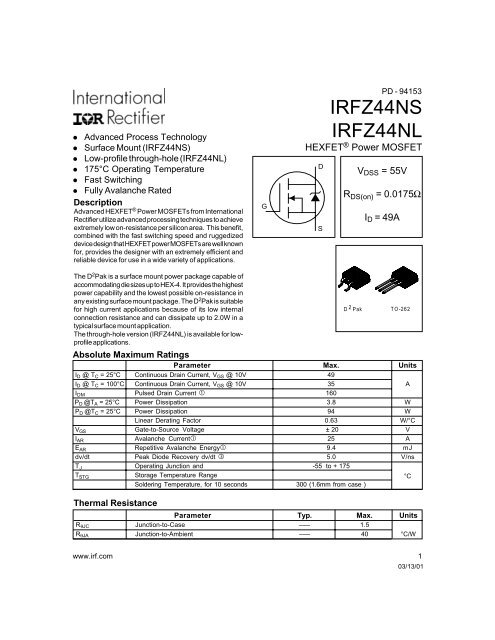
IRFZ44NS/IRFZ44NLElectrical Characteristics @ T J = 25°C (unless otherwise specified)Parameter Min. Typ. Max. Units ConditionsV (BR)DSS Drain-to-Source Breakdown Voltage 55 ––– ––– V V GS = 0V, I D = 250µA∆V (BR)DSS /∆T J Breakdown Voltage Temp. Coefficient ––– 0.058 ––– V/°C Reference to 25°C, I D = 1mAR DS(on) Static Drain-to-Source On-Resistance ––– ––– 17.5 mΩ V GS = 10V, I D = 25A „V GS(th) Gate Threshold Voltage 2.0 ––– 4.0 V V DS = V GS , I D = 250µAg fs Forward Transconductance 19 ––– ––– S V DS = 25V, I D = 25A„I DSS Drain-to-Source Leakage Current––– ––– 25 VµA DS = 55V, V GS = 0V––– ––– 250 V DS = 44V, V GS = 0V, T J = 150°CI GSSGate-to-Source Forward Leakage ––– ––– 100 V GS = 20VnAGate-to-Source Reverse Leakage ––– ––– -100 V GS = -20VQ g Total Gate Charge ––– ––– 63 I D = 25AQ gs Gate-to-Source Charge ––– ––– 14 nC V DS = 44VQ gd Gate-to-Drain ("Miller") Charge ––– ––– 23 V GS = 10V, See Fig. 6 and 13t d(on) Turn-On Delay Time ––– 12 ––– V DD = 28Vt r Rise Time ––– 60 ––– I D = 25Anst d(off) Turn-Off Delay Time ––– 44 ––– R G = 12Ωt f Fall Time ––– 45 ––– V GS = 10V, See Fig. 10 „L S Internal Source Inductance ––– 7.5 ––– nH Between lead,and center of die contactC iss Input Capacitance ––– 1470 ––– V GS = 0VC oss Output Capacitance ––– 360 ––– V DS = 25VC rss Reverse Transfer Capacitance ––– 88 ––– pF ƒ = 1.0MHz, See Fig. 5E AS Single Pulse Avalanche Energy‚ ––– 530… 150† mJ I AS = 25A, L = 0.47mHSource-Drain Ratings and CharacteristicsParameter Min. Typ. Max. Units ConditionsDI S Continuous Source Current MOSFET symbol––– ––– 49(Body Diode)showing theAGI SM Pulsed Source Current integral reverse––– ––– 160(Body Diode)p-n junction diode.SV SD Diode Forward Voltage ––– ––– 1.3 V T J = 25°C, I S = 25A, V GS = 0V „t rr Reverse Recovery Time ––– 63 95 ns T J = 25°C, I F = 25AQ rr Reverse Recovery Charge ––– 170 260 nC di/dt = 100A/µs „t on Forward Turn-On Time Intrinsic turn-on time is negligible (turn-on is dominated by L S +L D )Notes:Repetitive rating; pulse width limited bymax. junction temperature. (See fig. 11)‚ Starting T J = 25°C, L = 0.48mHR G = 25Ω, I AS = 25A. (See Figure 12)ƒ I SD ≤ 25A, di/dt ≤ 230A/µs, V DD ≤ V (BR)DSS ,T J ≤ 175°C„ Pulse width ≤ 400µs; duty cycle ≤ 2%.… This is a typical value at device destruction and representsoperation outside rated limits.† This is a calculated value limited to T J = 175°C .** When mounted on 1" square PCB (FR-4 or G-10 Material ).For recommended footprint and soldering techniques refer to application note #AN-994.2 www.irf.com
IRFZ44NS/IRFZ44NLI , Drain-to-Source Current (A)D100010010VGSTOP 15V10V8.0V7.0V6.0V5.5V5.0VBOTTOM 4.5V4.5VI , Drain-to-Source Current (A)D100010010VGSTOP 15V10V8.0V7.0V6.0V5.5V5.0VBOTTOM 4.5V4.5V20µs PULSE W IDTH20µs PULSE WIDTHT 1J C= 25°C ATCJ = 175°C1A0.1 1 10 1000.1 1 10 100VDS, Drain-to-Source Voltage (V )V , Drain-to-Source Voltage (V )DSFig 1. Typical Output CharacteristicsFig 2. Typical Output CharacteristicsI D , Drain-to-Source Current (A)100010010T = 25°CJT = 175°CJV DS = 25V20µs PULSE WIDTH1A4 5 6 7 8 9 10V GS , Gate-to-Source Voltag e (V)Fig 3. Typical Transfer CharacteristicsR DS(on) , Drain-to-Source O n R esistance(Normalized)2.52.01.51.00.5I D = 41AV GS = 10V0.0A-60 -40 -20 0 20 40 60 80 100 120 140 160 180T J, Junction Temperature (°C)Fig 4. Normalized On-ResistanceVs. Temperaturewww.irf.com 3
IRFZ44NS/IRFZ44NLC, Capacitance (pF)2500200015001000500C issC ossV GS = 0V, f = 1MHzC iss = C g s + C g d , C ds SHORTEDC rss = C g dC oss = C ds + C gdC rss0V , Gate-to-Source Voltage (V)GS20161284I D = 25AV DS = 44VV DS = 28V0A1 10 100V DS , Drain-to-Source Voltage (V )Fig 5. Typical Capacitance Vs.Drain-to-Source VoltageFOR TEST CIRCUITSEE FIGURE 13A0 10 20 30 40 50 60 70Q G , Total Gate Charge (nC)Fig 6. Typical Gate Charge Vs.Gate-to-Source VoltageI SD , Reverse Drain Current (A)100010010T = 175°CJT = 25°CJV GS = 0V1A0.5 1.0 1.5 2.0 2.5 3.0V SD , Source-to-Drain Voltage (V )Fig 7. Typical Source-Drain DiodeForward VoltageI D , Drain Current (A)1000100101OPERATION IN THIS AREA LIMITEDBY R DS(on)T C = 25°CT J = 175°CSing le P u lse10µs100µs1ms10ms1 10 100V DS , Drain-to-Source Voltage (V )Fig 8. Maximum Safe Operating AreaA4 www.irf.com
IRFZ44NS/IRFZ44NLV DSR D50R GV GSD.U.T.+- V DDI D , Drain Current (A)40302010Fig 10a. Switching Time Test CircuitV DS90%10VPulse Width ≤ 1 µsDuty Factor ≤ 0.1 %025 50 75 100 125 150 175T C , Case Temperature ( ° C)10%V GSt d(on) t r t d(off) t fFig 9. Maximum Drain Current Vs.Case TemperatureFig 10b. Switching Time Waveforms10Thermal Response (Z thJC )10.1D = 0.500.200.100.050.020.01SINGLE PULSE(THERMAL RESPONSE)Notes:1. Duty factor D = t 1 / t 22. Peak T J = P DM x Z thJC + TC0.010.00001 0.0001 0.001 0.01 0.1t 1, Rectangular Pulse Duration (sec)PDMt1t2Fig 11. Maximum Effective Transient Thermal Impedance, Junction-to-Casewww.irf.com 5
IRFZ44NS/IRFZ44NLLV DSD.U.T.R G +V- DD10 VI ASt p 0.01ΩFig 12a. Unclamped Inductive Test CircuitV (BR)DSSt pV DDE AS , Single Pulse Avalanche Energy (mJ)500400300200100TOPBOTTOMV DD = 25V0A25 50 75 100 125 150 175Starting T J , Junction Temperature (°C )ID10A18A25AV DSI ASFig 12b. Unclamped Inductive WaveformsFig 12c. Maximum Avalanche EnergyVs. Drain CurrentCurrent RegulatorSame Type as D.U.T.50KΩ10 VQ GSQ GQ GD12V.2µF.3µFD.U.T.+V- DSV GV GS3mAChargeI G I DCurrent Sampling ResistorsFig 13a. Basic Gate Charge WaveformFig 13b. Gate Charge Test Circuit6 www.irf.com
IRFZ44NS/IRFZ44NLPeak Diode Recovery dv/dt Test CircuitD.U.T+ƒ-Circuit Layout Considerations• Low Stray Inductance• Ground Plane• Low Leakage InductanceCurrent Transformer+‚--„+R G• dv/dt controlled by R G• Driver same type as D.U.T.• I SD controlled by Duty Factor "D"• D.U.T. - Device Under Test+-V DDDriver Gate DrivePeriodP.W.D =P.W.PeriodV GS =10V*D.U.T. I SD WaveformReverseRecoveryCurrentBody Diode ForwardCurrentdi/dtD.U.T. V DS WaveformDiode Recoverydv/dtV DDRe-AppliedVoltageInductor CurentBody DiodeForward DropRipple ≤ 5%I SD* V GS = 5V for Logic Level DevicesFig 14. For N-Channel HEXFETSwww.irf.com 7
IRFZ44NS/IRFZ44NLD 2 Pak Package Outline1.40 (.055)M AX.10.54 (.415)10.29 (.405)- A -24.69 (.185)4.20 (.165)- B -1.32 (.052)1.22 (.048)10.16 (.400)REF.6.47 (.255)6.18 (.243)1.78 (.070)1.27 (.050)1 315.49 (.610)14.73 (.580)2.79 (.110)2.29 (.090)5.28 (.208)4.78 (.188)2.61 (.103)2.32 (.091)3X1.40 (.055)1.14 (.045)5.08 (.200)3X0.93 (.037)0.69 (.027)0.55 (.022)0.46 (.018)1.39 (.055)1.14 (.045)8.89 (.350)REF.0.25 (.010) M B A M MINIMUM RE<strong>COM</strong>MENDED FOOTPRINT11.43 (.450)NOTES:1 DIMENSIONS AFTER SOLDER DIP.2 DIMENSIONING & TOLERANCING PER ANSI Y14.5M, 1982.3 CONTROLLING DIMENSION : INCH.4 HEATSINK & LEAD DIMENSIONS DO NOT INCLUDE BURRS.LEAD ASSIGNMENTS1 - GATE2 - DRAIN3 - SOURCE8.89 (.350)3.81 (.150)17.78 (.700)2.08 (.082)2X2.54 (.100)2XPart Marking InformationD 2 PakINTERNATIONALRECTIFIERLOGOASSEMBLYLOT CODEF530S92469B 1MPART NUMBERDATE CODE(YYW W )YY = YEARWW = WEEKA8 www.irf.com
IRFZ44NS/IRFZ44NLPackage OutlineTO-262 OutlinePart Marking InformationTO-262www.irf.com 9
IRFZ44NS/IRFZ44NLTape & Reel InformationD 2 PakTRR4.10 (.16 1)3.90 (.15 3)1.60 (.063)1.50 (.059)1.60 (.063)1.50 (.059)0.368 (.0145)0.342 (.0135)FEED DIRECTIONTRL1.85 (.07 3)1.65 (.06 5)10.90 (.429)10.70 (.421)11.60 (.457)11.40 (.449)16.10 (.634)15.90 (.626)1.75 (.069)1.25 (.049)15.42 (.609)15.22 (.601)24.30 (.957)23.90 (.941)4.72 (.136)4.52 (.178)FEED DIRECTION13.50 (.532)12.80 (.504)27.40 (1.079)23.90 (.941)4330.00(14.173)MAX.60.00 (2.362)MIN.NOTES :1. <strong>COM</strong>FORMS TO EIA-418.2. CONTROLLING DIMENSION: MILLIMETER.3. DIMENSION MEASURED @ HUB.4. INCLUDES FLANGE DISTORTION @ OUTER EDGE.26.40 (1.039)24.40 (.961)330.40 (1.197)MAX.4Data and specifications subject to change without notice.This product has been designed and qualified for the industrial market.Qualification Standards can be found on IR’s Web site.IR WORLD HEADQUARTERS: 233 Kansas St., El Segundo, California 90245, USA Tel: (310) 252-7105TAC Fax: (310) 252-7903Visit us at www.irf.com for sales contact information. 3/0110 www.irf.com