Gate Delay Propagation Delay Definitions DFF Timing
Gate Delay Propagation Delay Definitions DFF Timing
Gate Delay Propagation Delay Definitions DFF Timing

Create successful ePaper yourself
Turn your PDF publications into a flip-book with our unique Google optimized e-Paper software.
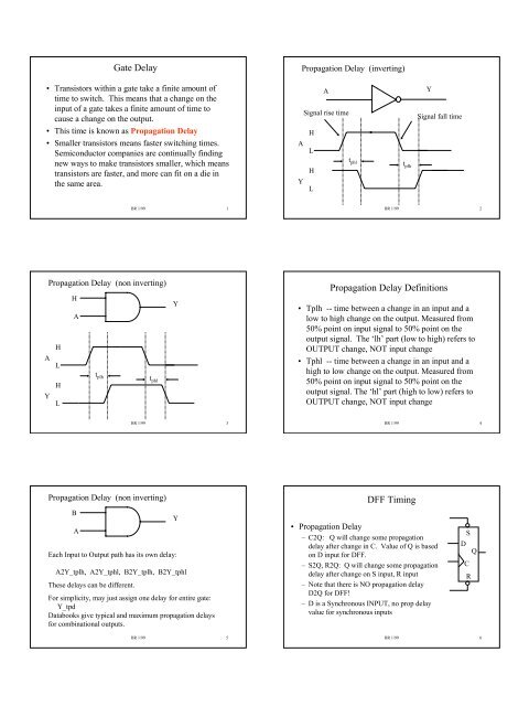
<strong>Gate</strong> <strong>Delay</strong><strong>Propagation</strong> <strong>Delay</strong> (inverting)• Transistors within a gate take a finite amount oftime to switch. This means that a change on theinput of a gate takes a finite amount of time tocause a change on the output.• This time is known as <strong>Propagation</strong> <strong>Delay</strong>• Smaller transistors means faster switching times.Semiconductor companies are continually findingnew ways to make transistors smaller, which meanstransistors are faster, and more can fit on a die inthe same area.ASignal rise timeHALHYLt phltplhYSignal fall timeBR 1/99 1BR 1/99 2<strong>Propagation</strong> <strong>Delay</strong> (non inverting)HAHALHYLt plhtphlY<strong>Propagation</strong> <strong>Delay</strong> <strong>Definitions</strong>• Tplh -- time between a change in an input and alow to high change on the output. Measured from50% point on input signal to 50% point on theoutput signal. The ‘lh’ part (low to high) refers toOUTPUT change, NOT input change• Tphl -- time between a change in an input and ahigh to low change on the output. Measured from50% point on input signal to 50% point on theoutput signal. The ‘hl’ part (high to low) refers toOUTPUT change, NOT input changeBR 1/99 3BR 1/99 4<strong>Propagation</strong> <strong>Delay</strong> (non inverting)BAEach Input to Output path has its own delay:A2Y_tplh, A2Y_tphl, B2Y_tplh, B2Y_tphlThese delays can be different.For simplicity, may just assign one delay for entire gate:Y_tpdDatabooks give typical and maximum propagation delaysfor combinational outputs.Y<strong>DFF</strong> <strong>Timing</strong>• <strong>Propagation</strong> <strong>Delay</strong>– C2Q: Q will change some propagationdelay after change in C. Value of Q is basedon D input for <strong>DFF</strong>.– S2Q, R2Q: Q will change some propagationdelay after change on S input, R input– Note that there is NO propagation delayD2Q for <strong>DFF</strong>!– D is a Synchronous INPUT, no prop delayvalue for synchronous inputsSDQCRBR 1/99 5BR 1/99 6
Setup, Hold Times• Synchronous inputs (e.g. D) have Setup, Holdtime specification with respect to the CLOCKinput• Setup Time: the amount of time the synchronousinput (D) must be stable before the active edge ofclock• Hold Time: the amount of time the synchronousinput (D) must be stable after the active edge ofclock.BR 1/99 7CD changingSetup, Hold Timet sut hdStableD changingIf changes on D input violate either setup or holdtime, then correct FF operation is not guaranteed.Setup/Hold measured around active clock edge.BR 1/99 8Sequential System <strong>Timing</strong>nk-bitPresent StateValuekCombinationalLogicCircuit<strong>DFF</strong>Q Dkmk-bitNext StateValueQuestion: What is the MAXIMUM frequency of operation ofthis system?Maximum Frequency = 1/ (longest delay path)What are longest paths???clkLongest Paths in Sequential System DiagramPaths to check:A. Clock to Output delay: Tc2q + Tcomb_Q2O maxTcomb_Q2O is longest path from Q output to any outputB. Register to Register delay: Tc2q + Tcomb_Q2D max + TsetupTcomb Q2D is longest path from Q dff output to D dff inputC. Pin to Pin combinational delay: Tcomb_I2O max(input pin to output pin, no intervening registers)Typically, path “B” is the worst case.BR 1/99 9BR 1/99 10Inputs/Outputs RegisteredVery often, all inputs and outputs are registered. Then registerto-registerdelay will almost always determine maximumfrequency.TsetupD CombinationalN QDLogicK QC N Tpd maxC KC2Qdelay = Tc2q + Tpd max + TsetupDN QC NC2QHold Time and Shortest PathsCombinationalLogicTpd minTholdTo satisfy hold time:Tc2q + Tpd (minimum) >= TholdDK QCThis is normally easily satisfied in a sequentialsystem.KBR 1/99 11BR 1/99 12
DQCToggle Frequencytoggle frequency = 1 /(C2Q + Tsetup)assume wire delay is neglibleWhat about setup time?0Tc2q + Tpd (min) >= TholdTcq > Tholdassuming zero wire delayBR 1/99 13Setup, Hold Time for External InputsExternal inputs are buffered through pad drivers and may gothrough combinational logic before they reach a synchronousinput. This buffering adds propagation delay. How does thispropagation delay affect the EXTERNAL setup and hold time????DINThd, TsuCLKComb LogComb LogThd, TsuDQCASICWhat is Thd, Tsu for DIN? It is NOT the same as for Thd,Tsu of the internal D FF!!!!!!! Thd, Tsu for DIN isspecified in the DATASHEET for design.YBR 1/99 14Calculating External Setup timesCalculating External Hold timesDINCLKTpd DINComb LogComb LogTpd ClkTsuDQCASICDINCLKTpd DINComb LogComb LogTpd ClkTsuDQCASICWorst case setup time for DIN occurs when ‘DIN’ isDELAYED relative to CLK. Means clock edge arrivesearly, requiring DIN to be ready sooner.Din Setup = Tsu + Tpd DIN (max) - Tpd CLK (min)Worst case hold time for DIN occurs when ‘CLK’ isDELAYED relative to DIN. Means clock edge arrives late,requiring DIN to hold its value longer.Din Hold = Thd + Tpd CLK (max) - Tpd DIN (min)BR 1/99 15BR 1/99 16AA <strong>Timing</strong> Example1 nsU77 nsU1U2DD QQU4CCU59 ns<strong>DFF</strong>s :U6Y6 ns<strong>Timing</strong>sMax Register to Register <strong>Delay</strong>U2 Tc2q + U3 Tpd + U1 Tsu = 5 + 8 + 3 = 16 ns.A setup time = Tsu + A2D Tpd max - Clk Tpd min= Tsu + (Tpd U3 + Tpd U7) - Tpd U8= 3 + (8 + 1) - 2 = 10 nsCKU82 nsU38 nsTsu = 3 nsThd = 4 nsTc2q = 5 nsA hold time = Thd + Clk Tpd max - A2D Tpd min= Thd + Tpd U8 - (Tpd U4 + Tpd U7)= 4 + 2 - (7 + 1) = -2 nsBR 1/99 17BR 1/99 18
<strong>Timing</strong>s (Cont)Clock to Out= U8 Tpd + U2 Tc2q + U5 Tpd + U6 Tpd= 2 + 5 + 9 + 6 = 22 nsPin to Pin Combinational <strong>Delay</strong> (A to Y)= U7 Tpd + U5 Tpd + U6 Tpd= 1 + 9 + 6 = 16 nsMax Clock Freq = 1/ Max (Reg2reg, Clk2Out, Pin2Pin)= 1/ Max (16, 22, 16)= 45.5 MhzDataSheetParameter Description Min Max UnitsTclk Clock Period 22 nsFclk Clock Frequency 45.5 MhzAtsu A setup time 10 nsAthd A hold time -2 nsA2Y A to Y Tpd 16 nsCk2Y Clock to Y tpd 22 nsNegative hold times are typically specified as 0 ns.BR 1/99 19BR 1/99 20How do we improve timings?Register all Inputs, Outputs!1 nsAU8, <strong>DFF</strong>U5 U6YU77 ns6 nsU1U2 9 nsDDQQU4U9, <strong>DFF</strong>CCNew <strong>Timing</strong>sMax Register to Register <strong>Delay</strong>U2 Tc2q + U5 Tpd + U9 Tsu = 5 + 9 + 3 = 17 ns.A setup time = Tsu + A2D Tpd max - Clk Tpd min= Tsu + (Tpd U7) - Tpd U8= 3 + (1) - 2 = 2 nsCKU82 nsU38 ns<strong>DFF</strong>s :Tsu = 3 nsThd = 4 nsTc2q = 5 nsA hold time = Thd + Clk Tpd max - A2D Tpd min= Thd + Tpd U8 - (Tpd U7)= 4 + 2 - ( 1) = 5 nsBR 1/99 21BR 1/99 22New DataSheetParameter Description Min Max UnitsTclk Clock Period 17 nsFclk Clock Frequency 58.8 MhzAtsu A setup time 2 nsAthd A hold time 5 nsCk2Y Clock to Y tpd 13 nsMost designs have all inputs, outputs registered.How does a PLL/DLL help?• A Phased Locked Loop or <strong>Delay</strong> Locked Loopcircuit is used to align the external clock edge at thepin with the internal clock edges at the <strong>DFF</strong> clkpins– Some clock skew due to clock routing network fromPLL will still be present, but input buffer delayeliminated.• This means that we can drop out the Clk Tpd termfrom the equations• How does this change things?BR 1/99 23BR 1/99 24
Without PLLBuffer <strong>Delay</strong>With PLLBuffer <strong>Delay</strong> eliminatedExtCKExtCKIntCKIntCKExtCKDQDQCCIO Buffer <strong>Delay</strong>IntCKBR 1/99 25ExtCKPLLIO Buffer <strong>Delay</strong>DQCIntCKDQCBR 1/99 26New <strong>Timing</strong>s (PLL, Inputs/Outputs Reg)New <strong>Timing</strong>s (PLL, Inputs/Outputs Reg)Max Register to Register <strong>Delay</strong>U2 Tc2q + U5 Tpd + U9 Tsu = 5 + 9 + 3 = 17 ns.A setup time = Tsu + A2D Tpd max - Clk Tpd min= Tsu + (Tpd U7) - 0 (due to PLL)= 3 + (1) - 0 = 4 nsA hold time = Thd + Clk Tpd max - A2D Tpd min= Thd + 0 (due to PLL) - (Tpd U7)= 4 + 0 - ( 1) = 3 nsClock to Out= U8 Tpd + U9 Tc2q + U6 Tpd= 0 (due to PLL) + 5 + 6 = 11 nsNO pin to Pin combinational delay! All inputs/outputsregistered!Max Clock Freq = 1/ Max (Reg2reg, Clk2Out, Pin2Pin)= 1/ Max (17, 11, 0)= 58.8 MhzBR 1/99 27BR 1/99 28New DataSheet (PLL, Inputs/Outputs Reg)Parameter Description Min Max UnitsTclk Clock Period 17 nsFclk Clock Frequency 58.8 MhzAtsu A setup time 4 nsAthd A hold time 3 nsInputsChip to Chip <strong>Timing</strong> CalculationASIC #1 ASIC #2Ck2Y Clock to Y tpd 11 nsClock to Output improved; important in multiple chipdesigns. External Setup/Hold times closer to setup/holdtimes of internal <strong>DFF</strong>s.CLKNeed to know external setup/hold times all inputs, clk to outof all outputs, all pin to pin combinational delays.ASIC = Application Specific Integrated CircuitBR 1/99 29BR 1/99 30
Max Register to Register <strong>Delay</strong>2 ASIC SystemAssume no pin to pin combinational delays and that inputs/outputsof both ASICs are registered.For any outputs from ASIC #1 which are Inputs to ASIC #2 findmaximum of ASIC #1 Clk to out + ASIC#2 Setup time.For any outputs from ASIC #2 which are Inputs to ASIC #1 findmaximum of ASIC #2 Clk to out + ASIC#1 Setup time.The maximum of these two times will be the minimum clockperiod.BR 1/99 31Other Factors that effect <strong>Timing</strong>• Voltage: the higher the voltage, the faster thatgates switch• Temperature: the lower the temperature, the fasterthat gates switch• Process Technology (transistor gate width). Theshorter the transistor gate length, the faster thetransistor will switch (I.e, 0.5u process versus0.35u process).• In a given process run, may get fast N transistors,fast P transistors, slow N transistors, slow PtransitorsBR 1/99 32Device Characterization• Do timing analysis on ASICs at four extremecorners to make sure they meet timing specs underall conditions• Fastest Case: Fast N transistors, Fast P transistors,High Vdd, Low temperature• Slowest Case: Slow N transistors, slow Ptransistors, low Vdd, high temperature• Other two corners can vary but two possiblecorners are:– Fast N, Slow P, Typical Temperature– Slow N, Fast P, Typical TemperatureBR 1/99 33Speed Grades• Databooks often list different speed grades for apart at the same temperature• Simply test parts that come off the fabrication lineand see how fast they are– Divide the parts into different speed bins– For three speed grades, a design goal might be to have15% of your parts fall in the upper bin, 50% in themiddle bin, and 25% in the lower bin.– As the process matures, more and more fabricated partswill move into the upper speed bin, at which point youmake a new upper speed bin.– Obviously, faster parts cost more (and are moreprofitable)BR 1/99 34Static Path Analysis• After your gate netlist has been mapped to theFPGA, a timing analysis tool will analyze the pathsin the design and compute the timings we havediscussed• The timing analyzer takes into account the routingdelays in the physical routing and the speed gradeof the part you have mapped to.– Because routing can sometimes change somewhatdrastically for even small changes, often try run multipledevice mappings to try to get a ‘good route’.Static <strong>Timing</strong> Analysis Reports• The static timing analyzer will report the followingtimes– Register to Register delays– Setup times of all external synchronous inputs– Clock to Output delays– Pin to Pin combinational delays• The clock to output delay is usually just reported assimply another pin-to-pin combinational delay• <strong>Timing</strong> analysis reports are often pessimistic sincethey use worst case conditionsBR 1/99 35BR 1/99 36
<strong>Timing</strong> Simulation• The timings extracted by the <strong>Timing</strong> analysis tool(routing delays, gate delays for a particular speedgrade, etc) are used in the simulation• It may be tempting to simply ignore the delaysreported by the timing analyzer, and simplysimulate the design ‘at speed’ to see if it works.– If the design simulates correctly, only means that itworks for the particular test vectors that you used!– Different test vectors exercise different delay paths - youmust use test vectors that exercise the LONGEST pathsBR 1/99 37