- Page 2:
The Electrical Engineering Handbook
- Page 8:
The Electrical Engineering Handbook
- Page 12:
Published in 2006 byCRC PressTaylor
- Page 16:
with the structure, organization, a
- Page 22:
Advisory BoardFrank BarnesUniversit
- Page 28:
E.J. KennedyUniversity of Tennessee
- Page 34:
ContentsSECTION IElectronics1 Semic
- Page 38:
18 Microwave Devices18.1 Passive Mi
- Page 44:
I -2Electronics, Power Electronics,
- Page 48:
1 -2 Electronics, Power Electronics
- Page 52:
1 -4 Electronics, Power Electronics
- Page 56:
1 -6 Electronics, Power Electronics
- Page 60:
1 -8 Electronics, Power Electronics
- Page 64:
1 -10 Electronics, Power Electronic
- Page 68:
1 -12 Electronics, Power Electronic
- Page 72:
1 -14 Electronics, Power Electronic
- Page 76:
1 -16 Electronics, Power Electronic
- Page 80:
1 -18 Electronics, Power Electronic
- Page 84:
1 -20 Electronics, Power Electronic
- Page 88:
1 -22 Electronics, Power Electronic
- Page 92:
1 -24 Electronics, Power Electronic
- Page 96:
1 -26 Electronics, Power Electronic
- Page 100:
1 -28 Electronics, Power Electronic
- Page 104:
1 -30 Electronics, Power Electronic
- Page 108:
1 -32 Electronics, Power Electronic
- Page 112:
1 -34 Electronics, Power Electronic
- Page 116:
1 -36 Electronics, Power Electronic
- Page 120:
1 -38 Electronics, Power Electronic
- Page 126:
2SemiconductorManufacturingHarold G
- Page 130:
Semiconductor Manufacturing2-3for t
- Page 134:
Semiconductor Manufacturing2-5oxida
- Page 138:
Semiconductor Manufacturing2-7In th
- Page 142:
Semiconductor Manufacturing2-9direc
- Page 146:
Semiconductor Manufacturing2-11Latt
- Page 150:
Semiconductor Manufacturing2-13reac
- Page 154:
Semiconductor Manufacturing2-15Si 3
- Page 158:
Semiconductor Manufacturing2-17A. H
- Page 162:
Semiconductor Manufacturing2-19FIGU
- Page 166:
Semiconductor Manufacturing2-21FIGU
- Page 170:
Semiconductor Manufacturing2-23FIGU
- Page 174:
Semiconductor Manufacturing2-25TABL
- Page 178:
Semiconductor Manufacturing2-27FIGU
- Page 182:
Semiconductor Manufacturing2-29FIGU
- Page 186:
Semiconductor Manufacturing2-31line
- Page 190:
Semiconductor Manufacturing2-33but
- Page 194:
Semiconductor Manufacturing2-35wher
- Page 198:
Semiconductor Manufacturing2-37FIGU
- Page 202:
Semiconductor Manufacturing2-39FIGU
- Page 206:
Semiconductor Manufacturing2-41FIGU
- Page 210:
Semiconductor Manufacturing2-43K NE
- Page 214:
Semiconductor Manufacturing2-45depe
- Page 218:
Semiconductor Manufacturing2-47FIGU
- Page 222:
Semiconductor Manufacturing2-49FIGU
- Page 226:
Semiconductor Manufacturing2-51This
- Page 232:
2-54 Electronics, Power Electronics
- Page 236:
2-56 Electronics, Power Electronics
- Page 240:
2-58 Electronics, Power Electronics
- Page 244:
2-60 Electronics, Power Electronics
- Page 248:
2-62 Electronics, Power Electronics
- Page 252:
2-64 Electronics, Power Electronics
- Page 256:
2-66 Electronics, Power Electronics
- Page 260:
2-68 Electronics, Power Electronics
- Page 266:
3TransistorsSidney SoclofCalifornia
- Page 270:
Transistors3 -3FIGURE 3.4shown in F
- Page 274:
Transistors3 -5The voltage source m
- Page 278:
Transistors3 -7FIGURE 3.9 FIGURE 3.
- Page 282:
Transistors3 -9drop across the drai
- Page 286:
Transistors3 -11The output voltage
- Page 290:
Transistors3 -13constant on the out
- Page 294:
Transistors3 -15The drain-to-source
- Page 298:
Transistors3 -17FIGURE 3.25The bipo
- Page 302:
Transistors3 -19I E ¼ I B þ h FE
- Page 306:
Transistors3 -21In the present case
- Page 310:
Transistors3 -23The magnitude and p
- Page 314:
Transistors3 -25FIGURE 3.32The load
- Page 318:
Transistors3 -27However, the small-
- Page 322:
Transistors3 -29FIGURE 3.34An emitt
- Page 326:
Transistors3 -31FIGURE 3.36Simplifi
- Page 330:
Transistors3 -33FIGURE 3.38Twodegen
- Page 334:
Transistors3 -35However:R emitterð
- Page 338:
Transistors3 -37This quiescent or b
- Page 342:
Transistors3 -393.3 The Metal-Oxide
- Page 346:
Transistors3 -41Strong-Inversion Ch
- Page 350:
Transistors3 -43no carriers present
- Page 354:
Transistors3 -45There are two more
- Page 358:
Transistors3 -47Equation (3.46) sug
- Page 362:
Transistors3 -49Subthreshold Contro
- Page 366:
Transistors3 -51of dopant ions that
- Page 370:
Transistors3 -533.4 Single-Electron
- Page 374:
Transistors3 -55Electrostatic Charg
- Page 378:
Transistors3 -57(a)E Fq 2 /2 CE F(b
- Page 382:
Transistors3 -59FIGURE 3.51Single-e
- Page 386:
Transistors3 -610rE(x)r+sx-q FxFIGU
- Page 390:
Transistors3 -633aF20 mV1aFR T=10M
- Page 394:
4Integrated CircuitsJoe E. BrewerUn
- Page 398:
Integrated Circuits4 -3FIGURE 4.2Li
- Page 402:
Integrated Circuits4 -5The starting
- Page 406:
Integrated Circuits4 -7FIGURE 4.6Fa
- Page 410:
Integrated Circuits4 -9FIGURE 4.9 A
- Page 414:
Integrated Circuits4 -11The goal is
- Page 418:
Integrated Circuits4 -13FIGURE 4.17
- Page 422:
Integrated Circuits4 -15+2-2-1da1 4
- Page 426:
Integrated Circuits4 -17diameter of
- Page 430:
Integrated Circuits4 -19123451 42 5
- Page 434:
Integrated Circuits4 -214.3 Applica
- Page 438:
Integrated Circuits4 -23FIGURE 4.25
- Page 442:
Integrated Circuits4 -25FIGURE 4.27
- Page 446:
Integrated Circuits4 -27FIGURE 4.29
- Page 450:
Integrated Circuits4 -29FIGURE 4.32
- Page 454:
Integrated Circuits4 -31interconnec
- Page 458:
Integrated Circuits4 -33currents on
- Page 462:
Integrated Circuits4 -35describe. I
- Page 466:
Integrated Circuits4 -37S.H. Hall,
- Page 470:
Integrated Circuits4 -39clocks per
- Page 474:
Integrated Circuits4 -41Microcontro
- Page 478:
Integrated Circuits4 -43INPUT(ƒ)ƒ
- Page 482:
Integrated Circuits4 -45EnableAACom
- Page 486:
Integrated Circuits4 -47presenting
- Page 490:
Integrated Circuits4 -49TABLE 4.5 C
- Page 494:
Integrated Circuits4 -51submicron t
- Page 498:
Integrated Circuits4 -53have tobesa
- Page 502:
5Surface MountTechnologyGlenn R. Bl
- Page 506:
Surface Mount Technology5 -3. Assem
- Page 510:
Surface Mount Technology5 -5Again,
- Page 514: Surface Mount Technology5 -7FIGURE
- Page 518: Surface Mount Technology5 -9semicon
- Page 522: Surface Mount Technology5 -11One-pa
- Page 526: Surface Mount Technology5 -13Syring
- Page 530: Surface Mount Technology5 -155.9 Pa
- Page 534: Surface Mount Technology5 -17Checks
- Page 538: Surface Mount Technology5 -19FIGURE
- Page 542: Surface Mount Technology5 -21Gull w
- Page 546: 6Ideal and PracticalModelsE.J. Kenn
- Page 550: Ideal and Practical Models6 -3FIGUR
- Page 554: Ideal and Practical Models6 -5A OL
- Page 558: Ideal and Practical Models6 -7FIGUR
- Page 562: Ideal and Practical Models6 -9FIGUR
- Page 570: Amplifiers7 -3equations:V BB ¼ V T
- Page 574: Amplifiers7 -5FIGURE 7.8 Complement
- Page 578: Amplifiers7 -7ReferencesP.R. Gray a
- Page 582: Amplifiers7 -9FIGURE 7.12 (a) Schem
- Page 586: Amplifiers7 -11FIGURE 7.13The hybri
- Page 590: Amplifiers7 -13andR CO ¼ R LTð 7
- Page 594: Amplifiers7 -15appreciable load on
- Page 598: Amplifiers7 -17whereR C p ¼R p jj
- Page 602: Amplifiers7 -19With R o ignored:R C
- Page 606: 8Active FiltersJohn E. AyersUnivers
- Page 610: Active Filters8 -3TABLE 8.1Butterwo
- Page 614:
Active Filters8 -5TABLE 8.2 Chebysh
- Page 618:
Active Filters8 -7TABLE 8.4Chebyshe
- Page 622:
Active Filters8 -9TABLE 8.6Bessel P
- Page 626:
Active Filters8 -11TABLE 8.8Ellipti
- Page 630:
Active Filters8 -13Fifth-Order Cheb
- Page 634:
Active Filters8 -15If the section o
- Page 638:
Active Filters8 -17Now that the pro
- Page 642:
Active Filters8 -198.2 RealizationJ
- Page 646:
Active Filters8 -21functions, ladde
- Page 650:
Active Filters8 -23As in the case o
- Page 654:
Active FiltersT ð s Þ¼H ð s 2
- Page 658:
9Power ElectronicsAndrew MarshallTe
- Page 662:
Power Electronics9 -3bypassing carr
- Page 666:
Power Electronics9 -5Some Darlingto
- Page 670:
Power Electronics9 -7The most commo
- Page 674:
Power Electronics9 -9T1Load Voltage
- Page 678:
Power Electronics9 -11Cycloconverte
- Page 682:
Power Electronics9 -13FIGURE 9.15Th
- Page 686:
Power Electronics9 -15FIGURE 9.18dc
- Page 690:
Power Electronics9 -17P.C. Sen, Thy
- Page 694:
Power Electronics9 -19FIGURE 9.20 P
- Page 698:
Power Electronics9 -21FIGURE 9.24(a
- Page 702:
Power Electronics9 -23FIGURE 9.28Fu
- Page 706:
Power Electronics9 -25FIGURE 9.32 (
- Page 710:
Power Electronics9 -27FIGURE 9.34 T
- Page 714:
Power Electronics9 -29FIGURE 9.36 (
- Page 718:
Power Electronics9 -31frequency cha
- Page 722:
Power Electronics9 -33with zero-cur
- Page 726:
Power Electronics9 -3515. G. Hua, C
- Page 730:
Power Electronics9 -37Q 4 —choppi
- Page 734:
Power Electronics9 -39FIGURE 9.47Fo
- Page 738:
Power Electronics9 -41FIGURE 9.50Sl
- Page 742:
Power Electronics9 -43Defining Term
- Page 746:
Power Electronics9 -45Current filam
- Page 750:
Power Electronics9 -47where t L is
- Page 754:
Power Electronics9 -49FIGURE 9.55 T
- Page 758:
Power Electronics9 -51primarily in
- Page 762:
Power Electronics9 -53FIGURE 9.60 (
- Page 766:
Power Electronics9 -55GateLight tri
- Page 770:
Power Electronics9 -57FIGURE 9.64An
- Page 774:
Power Electronics9 -5911. A. Rosen
- Page 778:
Power Electronics9 -61FIGURE 9.65Ap
- Page 782:
Power Electronics9 -63FIGURE 9.68Ga
- Page 786:
Power Electronics9 -65v ai loadv bv
- Page 790:
Power Electronics9 -67FIGURE 9.72 C
- Page 794:
Power Electronics9 -69FIGURE 9.74 S
- Page 798:
Power Electronics9 -7124. P. Mattav
- Page 802:
Power Electronics9 -73UPS systems a
- Page 806:
Power Electronics9 -75ACMainsStatic
- Page 810:
Power Electronics9 -77ACMainsACDCDC
- Page 814:
Power Electronics9 -79ACMainsStatic
- Page 818:
Power Electronics9 -81Static Switch
- Page 822:
Power Electronics9 -83in many circu
- Page 826:
Power Electronics9 -85V ref+−Erro
- Page 830:
10OptoelectronicsJeff HechtLaser Fo
- Page 834:
Optoelectronics10-3FIGURE 10.1 Simp
- Page 838:
Optoelectronics10-5despite their lo
- Page 842:
Optoelectronics10-7where e is the d
- Page 846:
Optoelectronics10-9FIGURE 10.4 (a)
- Page 850:
Optoelectronics10-11Twomethods are
- Page 854:
Optoelectronics10-13Higher luminanc
- Page 858:
Optoelectronics10-15where u is the
- Page 862:
Optoelectronics10-17The output curr
- Page 866:
Optoelectronics10-19FIGURE 10.13The
- Page 870:
Optoelectronics10-21Light falling o
- Page 874:
Optoelectronics10-23Defining TermsC
- Page 878:
Optoelectronics10-25integrated on t
- Page 882:
Optoelectronics10-27FIGURE 10.21Ele
- Page 886:
Optoelectronics10-29FIGURE 10.24Dir
- Page 890:
Optoelectronics10-31FIGURE 10.27Pro
- Page 894:
Optoelectronics10-33ApplicationsMan
- Page 898:
Optoelectronics10-35Further Informa
- Page 904:
11-2 Electronics, Power Electronics
- Page 908:
11-4 Electronics, Power Electronics
- Page 912:
11-6 Electronics, Power Electronics
- Page 916:
11-8 Electronics, Power Electronics
- Page 920:
11-10 Electronics, Power Electronic
- Page 924:
11-12 Electronics, Power Electronic
- Page 930:
12Digital and AnalogElectronic Desi
- Page 934:
Digital and Analog Electronic Desig
- Page 938:
Digital and Analog Electronic Desig
- Page 942:
Digital and Analog Electronic Desig
- Page 946:
Digital and Analog Electronic Desig
- Page 950:
Digital and Analog Electronic Desig
- Page 954:
Digital and Analog Electronic Desig
- Page 958:
Digital and Analog Electronic Desig
- Page 962:
Digital and Analog Electronic Desig
- Page 966:
Digital and Analog Electronic Desig
- Page 972:
13-2 Electronics, Power Electronics
- Page 976:
13-4 Electronics, Power Electronics
- Page 980:
13-6 Electronics, Power Electronics
- Page 984:
13-8 Electronics, Power Electronics
- Page 988:
13-10 Electronics, Power Electronic
- Page 992:
13-12 Electronics, Power Electronic
- Page 996:
13-14 Electronics, Power Electronic
- Page 1002:
14Electromagnetic FieldsBanmali S.R
- Page 1006:
Electromagnetic Fields14-3d E nd E
- Page 1010:
Electromagnetic Fields14-5The term
- Page 1014:
Electromagnetic Fields14-7For apoin
- Page 1018:
Electromagnetic Fields14-9Ampere’
- Page 1022:
Electromagnetic Fields14-11Magnetic
- Page 1026:
Electromagnetic Fields14-13If we co
- Page 1032:
15-2 Electronics, Power Electronics
- Page 1036:
15-4 Electronics, Power Electronics
- Page 1040:
15-6 Electronics, Power Electronics
- Page 1044:
15-8 Electronics, Power Electronics
- Page 1048:
15-10 Electronics, Power Electronic
- Page 1052:
15-12 Electronics, Power Electronic
- Page 1056:
15-14 Electronics, Power Electronic
- Page 1060:
15-16 Electronics, Power Electronic
- Page 1064:
15-18 Electronics, Power Electronic
- Page 1068:
15-20 Electronics, Power Electronic
- Page 1072:
15-22 Electronics, Power Electronic
- Page 1076:
15-24 Electronics, Power Electronic
- Page 1082:
16Wave PropagationMatthew N.O. Sadi
- Page 1086:
Wave Propagation16-3where g ¼ a þ
- Page 1090:
Wave Propagation16-5TABLE 16.1Atten
- Page 1094:
Wave Propagation16-7a correction fa
- Page 1098:
Wave Propagation16-9FIGURE 16.5Geom
- Page 1102:
Wave Propagation16-11FIGURE 16.6 Ro
- Page 1106:
Wave Propagation16-13The cumulative
- Page 1110:
Wave Propagation16-15TM modes:EH mo
- Page 1114:
Wave Propagation16-17surfaces form
- Page 1118:
Wave Propagation16-19FIGURE 16.11Ac
- Page 1122:
Wave Propagation16-21TABLE 16.5Stan
- Page 1126:
Wave Propagation16-23FIGURE 16.15 V
- Page 1130:
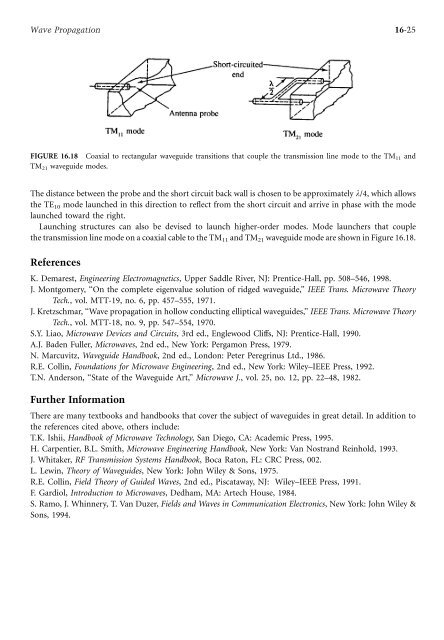
Wave Propagation16-25FIGURE 16.18 C
- Page 1136:
17-2 Electronics, Power Electronics
- Page 1140:
17-4 Electronics, Power Electronics
- Page 1144:
17-6 Electronics, Power Electronics
- Page 1148:
17-8 Electronics, Power Electronics
- Page 1152:
17-10 Electronics, Power Electronic
- Page 1156:
17-12 Electronics, Power Electronic
- Page 1160:
17-14 Electronics, Power Electronic
- Page 1164:
17-16 Electronics, Power Electronic
- Page 1168:
17-18 Electronics, Power Electronic
- Page 1172:
17-20 Electronics, Power Electronic
- Page 1176:
17-22 Electronics, Power Electronic
- Page 1180:
17-24 Electronics, Power Electronic
- Page 1186:
18Microwave DevicesMichael B.SteerN
- Page 1190:
Microwave Devices18-3Using travelin
- Page 1194:
Microwave Devices18-5Most passive d
- Page 1198:
Microwave Devices18-7FIGURE 18.5 Te
- Page 1202:
Microwave Devices18-9provide anumbe
- Page 1206:
Microwave Devices18-11transmission
- Page 1210:
Microwave Devices18-13FIGURE 18.11
- Page 1214:
Microwave Devices18-15maximum RF vo
- Page 1218:
Microwave Devices18-17FIGURE 18.13
- Page 1222:
Microwave Devices18-19FIGURE 18.14
- Page 1226:
Microwave Devices18-21Comparison of
- Page 1230:
19CompatibilityLeland H. HemmingMcD
- Page 1234:
Compatibility19-3Cable shield groun
- Page 1238:
Compatibility19-5TABLE 19.1 Absorpt
- Page 1242:
Compatibility19-7FIGURE 19.6Methods
- Page 1246:
Compatibility19-9Shield Seams. All
- Page 1250:
Compatibility19-11FIGURE 19.11chara
- Page 1254:
Compatibility19-13TEMPEST: Acode wo
- Page 1258:
Compatibility19-15Spectrum Specific
- Page 1262:
Compatibility19-17ySourcezElectricF
- Page 1266:
Compatibility19-19TABLE 19.4 Exampl
- Page 1270:
Compatibility19-21guidelines in con
- Page 1274:
Compatibility19-23the standards and
- Page 1278:
Compatibility19-25TABLE 19.13The CI
- Page 1282:
Compatibility19-27H. Eren, Electron
- Page 1286:
Compatibility19-29Commonly used rel
- Page 1290:
Compatibility19-31FIGURE 19.20 Meas
- Page 1294:
Compatibility19-33Modeling the Retu
- Page 1298:
Compatibility19-35corona envelope w
- Page 1302:
Compatibility19-37FIGURE 19.23 Exam
- Page 1306:
Compatibility19-39FIGURE 19.25 Meas
- Page 1310:
Compatibility19-41Y.T. Lin, M.A. Um
- Page 1314:
20RadarMelvin L. BelcherGeorgia Tec
- Page 1318:
Radar20-3techniques. As defined in
- Page 1322:
Radar20-5TABLE 20.2 Median Target R
- Page 1326:
Radar20-7pulse integration over agi
- Page 1330:
Radar20-9TABLE 20.4Typical Microwav
- Page 1334:
Radar20-11TABLE 20.6Selected Wavefo
- Page 1338:
Radar20-13textbook detection curves
- Page 1342:
Radar20-15Tracking Filter Performan
- Page 1346:
Radar20-17FIGURE 20.7 Waveforms for
- Page 1350:
Radar20-19mixer.After mixing with t
- Page 1354:
Radar20-21and for atriangle wave th
- Page 1358:
Radar20-23derivedfrom the returned
- Page 1362:
Radar20-25FIGURE 20.11 Honeywell 35
- Page 1366:
Radar20-27TABLE 20.13 PILOT Mk3 FMC
- Page 1370:
Radar20-29Collins (Rockwell Interna
- Page 1376:
21-2 Electronics, Power Electronics
- Page 1380:
21-4 Electronics, Power Electronics
- Page 1384:
21-6 Electronics, Power Electronics
- Page 1388:
21-8 Electronics, Power Electronics
- Page 1392:
21-10 Electronics, Power Electronic
- Page 1396:
21-12 Electronics, Power Electronic
- Page 1400:
21-14 Electronics, Power Electronic
- Page 1404:
21-16 Electronics, Power Electronic
- Page 1408:
21-18 Electronics, Power Electronic
- Page 1412:
21-20 Electronics, Power Electronic
- Page 1416:
21-22 Electronics, Power Electronic
- Page 1420:
21-24 Electronics, Power Electronic
- Page 1424:
21-26 Electronics, Power Electronic
- Page 1428:
21-28 Electronics, Power Electronic
- Page 1432:
22-2 Electronics, Power Electronics
- Page 1436:
22-4 Electronics, Power Electronics
- Page 1440:
22-6 Electronics, Power Electronics
- Page 1444:
22-8 Electronics, Power Electronics
- Page 1448:
22-10 Electronics, Power Electronic
- Page 1452:
22-12 Electronics, Power Electronic
- Page 1456:
22-14 Electronics, Power Electronic
- Page 1460:
22-16 Electronics, Power Electronic
- Page 1464:
22-18 Electronics, Power Electronic
- Page 1470:
23ComputationalElectromagneticsMatt
- Page 1474:
Computational Electromagnetics23-3X
- Page 1478:
Computational Electromagnetics23-5t
- Page 1482:
Computational Electromagnetics23-7F
- Page 1486:
Computational Electromagnetics23-9w
- Page 1490:
Computational Electromagnetics23-11
- Page 1494:
Computational Electromagnetics23-13
- Page 1498:
Computational Electromagnetics23-15
- Page 1502:
Computational Electromagnetics23-17
- Page 1506:
Computational Electromagnetics23-19
- Page 1510:
Computational Electromagnetics23-21
- Page 1514:
Computational Electromagnetics23-23
- Page 1518:
Computational Electromagnetics23-25
- Page 1522:
IIIElectrical Effectsand Devices24
- Page 1528:
24-2 Electronics, Power Electronics
- Page 1532:
24-4 Electronics, Power Electronics
- Page 1536:
24-6 Electronics, Power Electronics
- Page 1540:
24-8 Electronics, Power Electronics
- Page 1544:
25-2 Electronics, Power Electronics
- Page 1548:
25-4 Electronics, Power Electronics
- Page 1552:
25-6 Electronics, Power Electronics
- Page 1556:
25-8 Electronics, Power Electronics
- Page 1560:
25-10 Electronics, Power Electronic
- Page 1564:
25-12 Electronics, Power Electronic
- Page 1568:
25-14 Electronics, Power Electronic
- Page 1572:
26-2 Electronics, Power Electronics
- Page 1576:
26-4 Electronics, Power Electronics
- Page 1580:
26-6 Electronics, Power Electronics
- Page 1584:
26-8 Electronics, Power Electronics
- Page 1588:
27-2 Electronics, Power Electronics
- Page 1592:
27-4 Electronics, Power Electronics
- Page 1596:
27-6 Electronics, Power Electronics
- Page 1600:
28-2 Electronics, Power Electronics
- Page 1604:
28-4 Electronics, Power Electronics
- Page 1608:
28-6 Electronics, Power Electronics
- Page 1612:
28-8 Electronics, Power Electronics
- Page 1616:
28-10 Electronics, Power Electronic
- Page 1620:
29-2 Electronics, Power Electronics
- Page 1624:
29-4 Electronics, Power Electronics
- Page 1628:
29-6 Electronics, Power Electronics
- Page 1632:
29-8 Electronics, Power Electronics
- Page 1636:
29-10 Electronics, Power Electronic
- Page 1640:
29-12 Electronics, Power Electronic
- Page 1644:
29-14 Electronics, Power Electronic
- Page 1648:
TABLE 29.2MaterialElectrical and Ph
- Page 1652:
29-18 Electronics, Power Electronic
- Page 1656:
29-20 Electronics, Power Electronic
- Page 1660:
IV-2Mathematics, Symbols, and Physi
- Page 1664:
IV-4Mathematics, Symbols, and Physi
- Page 1668:
IV-6Mathematics, Symbols, and Physi
- Page 1672:
IV-8Mathematics, Symbols, and Physi
- Page 1676:
IV-10Mathematics, Symbols, and Phys
- Page 1680:
IV-12Mathematics, Symbols, and Phys
- Page 1684:
IV-14Mathematics, Symbols, and Phys
- Page 1688:
IV-16Mathematics, Symbols, and Phys
- Page 1692:
IV-18Mathematics, Symbols, and Phys
- Page 1696:
IV-20Mathematics, Symbols, and Phys
- Page 1702:
Author IndexAAgbo, Samuel O., Light
- Page 1706:
Author IndexA -3WWait, John V., Ide
- Page 1712:
S -2Electronics, Power Electronics,
- Page 1716:
S -4Electronics, Power Electronics,
- Page 1720:
S -6Electronics, Power Electronics,
- Page 1724:
S -8Electronics, Power Electronics,
- Page 1728:
S -10Electronics, Power Electronics
- Page 1732:
S -12Electronics, Power Electronics
- Page 1736:
S -14Electronics, Power Electronics
- Page 1740:
S -16Electronics, Power Electronics
- Page 1744:
S -18Electronics, Power Electronics
- Page 1748:
S -20Electronics, Power Electronics
- Page 1752:
S -22Electronics, Power Electronics
- Page 1756:
S -24Electronics, Power Electronics
- Page 1760:
S -26Electronics, Power Electronics
- Page 1764:
S -28Electronics, Power Electronics
- Page 1768:
S -30Electronics, Power Electronics
- Page 1772:
S -32Electronics, Power Electronics