
Create successful ePaper yourself
Turn your PDF publications into a flip-book with our unique Google optimized e-Paper software.
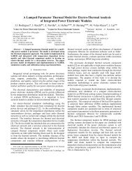
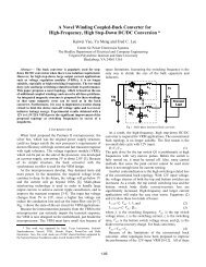
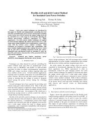
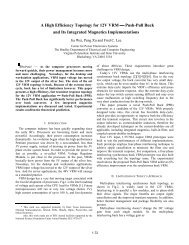
Characterization of Paralleled Super Junction MOSFET Devices under Hard- <strong>and</strong><strong>Soft</strong>-<strong>Switching</strong> <strong>Conditions</strong>Xudong Huang, Huijie Yu, <strong>and</strong> Jih-Sheng LaiVirginia Polytechnic Institute <strong>and</strong> State UniversityCenter for Power Electronics Systems (<strong>CPES</strong>) *665 Whittemore HallBlacksburg, VA 24061-0111Abstract— The super junction (SJ) MOSFET exhibitsconduction <strong>and</strong> switching properties similar to those ofconventional power MOSFETs. In this paper, we investigatepossible benefits <strong>and</strong> problems associated with connecting SJMOSFET in parallel for high-power applications. Measuredcircuit performances of paralleled SJ MOSFET devices areevaluated under hard- <strong>and</strong> soft-switching conditions. Themeasurements include (1) turn-on <strong>and</strong> turn-off switching voltage<strong>and</strong> current comparison, (2) gate driver resistance effects oncurrent sharing between paralleled SJ MOSFET devices, <strong>and</strong> (3)SJ MOSFET body diode behavior under hard- <strong>and</strong> softswitchingconditions. Two test circuits are developed forparalleled SJ MOSFET evaluation. One is an auxiliary resonantsnubber chopper for the near zero-voltage switching test, <strong>and</strong>the other one is an auxiliary resonant snubber inverter for thetrue zero-voltage condition test. Experimental results indicatethat SJ MOSFET can be paralleled without the need for precisedevice matching if the gate drive resistances are closelymatched.I. INTRODUCTIONA new class of MOS-gated power semiconductordevices, the super junction (SJ) MOSFET, is considered abreakthrough device because it offers a much-reduced onresistancefor high voltage applications over the conventionalpower MOSFET [1]. This device exhibits conductionproperties similar to those of conventional power MOSFETswith positive temperature coefficients [2]. It is thereforeexpected that the SJ MOSFET can be used in parallelconfigurations under steady state conditions.Conventional power MOSFETs often are used in parallelconfigurations for higher power switching applications. Thepurpose of this paper is to study the dynamic current sharingbehavior of SJ MOSFET for parallel operation in both hard<strong>and</strong>soft-switching circuits.Conventional power MOSFETs <strong>and</strong> SJ MOSFETdevices suffer effects of slow recovery of the drain-bodydiode. In chopper-type converters where the current flowsthrough an inductor in one direction, the commutating diodeturn-off current is diverted through a fast external diode, <strong>and</strong>* This work made use of ERC Shared Facilities supported by the NationalScience Foundation under Award Number EEC-9731677.† Contribution of the National Institute of St<strong>and</strong>ards <strong>and</strong> Technology <strong>and</strong>not subject to copyright.Allen R. Hefner, Jr., <strong>and</strong> David W. BerningNational Institute of St<strong>and</strong>ards <strong>and</strong> Technology †Semiconductor Electronics DivisionBuilding 225, Room B314Gaithersburg, MD 20899the associated MOSFET turn-on current does not contain alarge diode-recovery current transient. Therefore, the drainbodydiode in SJ MOSFET is not expected to restrict the useof paralleled SJ MOSFET devices in this type of converter.For two- <strong>and</strong> four-quadrant inverter applications, however, itis difficult to use MOSFET devices <strong>and</strong> parallel them for highpower applications due to the slow reverse recovery of thedrain-body diode.For hard-switching applications, a series diode can beused with the MOSFET to block the recovery of the drainbodydiode. An anti-parallel, fast-recovery diode can then beused in parallel with the MOSFET-series-diode combinationto implement commutation. The resulting device of thisremedy does not allow parallel-operation because the addeddiode has a negative temperature coefficient.An option that may allow parallel MOSFETs to be usedin inverter applications is the use of the zero-voltage softswitchingcircuit. This circuit temporarily diverts thefreewheeling or commutating diode current. This techniqueprovides extra time for the drain-body diode in the MOSFETto recover before voltage is reapplied [3–6].In this paper, the switching behavior of paralleled SJMOSFET devices under soft-switching conditions is studiedto explore the possibility of applying paralleled SJ MOSFETin high-power inverter applications. The experimental resultsindicate that SJ MOSFET can be paralleled without the needfor precise matching. However, the gate drive resistors needto be matched to ensure equal switching delays <strong>and</strong> thusequal dynamic current sharing. Under hard turn-onconditions, the differences between gate-drives resistancesrelatedswitching delays might cause the slower device to beover-stressed. Under the zero-voltage soft turn-on condition,the mismatch of gate resistances is less of a problem becausethe switching energy <strong>and</strong> stress are nearly zero. It is alsofound that better current sharing can be achieved with lowervaluegate resistors because the MOSFETs switch faster, <strong>and</strong>the periods of potential mismatch are reduced.II. ZERO-VOLTAGE SOFT-SWITCHING TEST CIRCUITSA. Device Test CircuitsTwo test circuits are developed for evaluating paralleledSJ MOSFET switching performance. The first one, shown inFig. 1, is an auxiliary resonant snubber chopper (ARSC).The second is an auxiliary resonant snubber inverter (ARSI),shown in Fig 2.
The ARSC circuit consists of a two-quadrant chopperwith two pairs of paralleled SJ MOSFET devices (S 1 , S 2 ) <strong>and</strong>(S 3, S 4 ), <strong>and</strong> the freewheeling diodes D 1 <strong>and</strong> D 2 . For soft turnoff,snubber capacitors C r are connected across the maindevices including the SJ MOSFET pairs <strong>and</strong> the freewheelingdiodes. An auxiliary resonant circuit that consists of anauxiliary switch S x , diode D x , <strong>and</strong> resonant inductor L r , isconnected across the inductive load L. Because the initialcondition of the resonant inductor current is not controllable,this type of circuit can achieve only near-zero-voltage turn-on[7]. The major components used in this circuit are listed asfollows:V sS 1 - S 4 : SJ MOSFET, rated 190 mΩ , 20 A, 600 VD 1 , D 2 : fast reverse recovery diode, rated 20 A, 600 VL: 2 mHL r : 3 µHC r : 0.027 µFR g4R S 3S 4 g3C rD C r 2LI LCinI Lr S xS 1S 2D C L rR g21 rD xR g1I s1I s2Fig. 1. The auxiliary resonant snubber chopper test circuit.The two freewheeling diodes, D 1 <strong>and</strong> D 2, can be replacedwith SJ MOSFET devices, <strong>and</strong> the test circuit becomes anauxiliary resonant snubber inverter (ARSI), as shown in Fig.2. By connecting gates <strong>and</strong> sources together, the twoparalleled switch pairs, (S 5, S 6 ) <strong>and</strong> (S 7, S 8 ), becomefreewheeling diodes, <strong>and</strong> the circuit operation is identical toFig. 1.C rIf the gate-sources of (S 5, S 6 ) <strong>and</strong> (S 7, S 8 ) switch pairs arecontrolled with pulse-width-modulation (PWM) signals, thenthe circuit becomes a four-quadrant, soft-switching chopperor inverter. In this case, D x needs to be changed to add ananti-paralleled switch to allow bi-directional, resonant currentcontrol. As described in [3], the circuit allows theestablishment of an initial resonant inductor current bykeeping (S 5, S 6 ) <strong>and</strong> (S 7, S 8 ) switch pairs on for a short periodat the beginning of resonance to achieve true zero-voltageturn-on.B. Switch TimingA two-pulse sequence strategy is used to gate the maindevices (S 1 , S 2 , <strong>and</strong> S 3 , S 4 ) with a fixed time period toestablish the desired load current in L. The soft-switchingoperation of the ARSI <strong>and</strong> ARSC circuits was previouslydescribed [7][8]. During turn-on, the resonant branch circuitdiverts the current in the freewheeling diode to the drainbodydiode <strong>and</strong> provides a zero-voltage condition to theMOSFET. During turn-off, the voltage rate of rise is reducedby snubber capacitor C r .Fig. 3 shows the gate signals <strong>and</strong> corresponding devicevoltage <strong>and</strong> current waveforms for the ARSC test circuit. TheSJ MOSFET devices are turned on with V gs at time t 1 , <strong>and</strong> theload inductor L is linearly charged with a di/dt = V s /L. Attime t 2 , the load current, I L , increases to (t 2 – t 1 )V s /L , <strong>and</strong> thetwo SJ MOSFET devices are turned off to discharge the loadcurrent. For the ARSC circuit, the freewheeling diodes, D 1<strong>and</strong> D 2 , are fast reverse recovery types. For the ARSI circuit,the slow recovery body diodes of SJ MOSFET devices (S 5 ~ S 8 )are used. Results for the ARSI circuit are shown in sectionIII. D. Between time t 3 <strong>and</strong> t 4, the auxiliary switch, S x , turnson with V Aux_GE , <strong>and</strong> the resonant branch circuit establishes aresonant current, I Lr , to divert the load current away from thefreewheeling diodes <strong>and</strong> allows the devices to be switchedunder the zero-voltage condition. The second V gs pulse startsright after the SJ MOSFET drain-source voltage, V ds , drops tozero. The purpose of this second pulse is to monitor the zerovoltageturn-on condition so it is typically a short pulse of afew microseconds.VgsV sR g4R S 3S 4 S 5S 6g3 C rIL LCinI Lr SS x7 S 8 S 1SC 2r L rD xR g2R g1I s1I s2C rC rVAux_GEVdsILILrTurn-offVSTurn-onFig. 2. The auxiliary resonant snubber inverter test circuit.t 0t 1t 2t 3t 4t 560.t 6Fig. 3. Corresponding gating signals <strong>and</strong> waveforms of the test circuits.
III. DEVICE CHARACTERIZATION RESULTSA. Turn-on CharacteristicFig. 4 shows the turn-on waveforms of the current <strong>and</strong>voltage of the SJ MOSFET under hard- <strong>and</strong> soft-switchingconditions in the ARSC tester at 300 V bus voltage <strong>and</strong> a loadcurrent of 40 A. Each device shares 20 A equally.It can be seen that the turn-on current of the SJ MOSFEThas an overshoot of 45 A with 225 A/µs rate under hardswitchingconditions. Under soft-switching conditions, thereis no overshoot current, <strong>and</strong> the current rise rate is reducedsignificantly. Notice that there is an initial current bump insoft turn-on because the device is not turned on at true zerovoltage, <strong>and</strong> a small voltage across the snubber capacitorneeds to be discharged when the device is gated on. Thisinitial current bump corresponds to the capacitor dischargecurrent. Its magnitude, however, is much smaller than thediode reverse recovery current under the hard-switchingcondition.10AV S1I S1Fig. 4(b) indicates that the intersection area of voltage<strong>and</strong> current diminishes, <strong>and</strong> the turn-on loss under softswitching is reduced drastically as compared with the hardswitchingcase. The turn-on energy can be obtained by theintegration of the intersection area.Fig. 5 shows the integration results of the turn-on energyfor both hard- <strong>and</strong> soft-switching conditions. The SJMOSFET turn-on energy under soft switching is reducedsignificantly compared to hard switching. At this 20 Acurrent condition, the turn-on energy is reduced from 1 mJ to0.12 mJ. The turn-on loss associated with soft switchingcomes from the zero crossing area, where the device voltageis not truly zero because it is tested with the ARSC circuit,which does not provide initial inductor boost current todischarge the resonant capacitor.turn-on loss (mJ1.41.210.80.60.40.2hard-switchingsoft-switching00 5 10 15 20 25device current (A)Fig. 5. Turn-on losses under hard- <strong>and</strong> soft-switching conditions.B. Turn-off Characteristic10A(a) Turn-on under hard switchingV S1I S1(b) Turn-on under soft switchingFig. 4. SJ MOSFET turn-on under hard- <strong>and</strong> soft-switchingconditions.Fig. 6 shows the turn-off waveforms of the current <strong>and</strong>voltage of the SJ MOSFET devices under hard- <strong>and</strong> softswitchingconditions in the ARSC test circuit at a 300 V bus<strong>and</strong> with a device current of 20 A. The dv/dt under hardswitching is about 3000 V/µs, while under soft switching it isabout 600 V/µs. The test results indicate that the turn-offvoltage has nearly zero overshoot voltage under both hard<strong>and</strong>soft-switching conditions. This can be attributed to agood circuit layout that involves minimum parasiticinductance.The turn-off energy, again, can be obtained from theintegration of the intersection area of the voltage <strong>and</strong> current.Fig. 7 shows the integration results at different currentconditions. It indicates that the turn-off energy is greatlyreduced because the resonant capacitor slows down the SJMOSFET voltage rise during turn-off, thus diminishing theintersection area of voltage <strong>and</strong> current. At the 20 Acondition, the turn-off loss is decreased from 0.55 mJ underhard switching to 0.12 mJ under soft switching.
10AI S1V S1(a) Turn-off under hard switchingthe ARSC circuit. For the current rise in the hard-switchingcondition, the device with smaller gate drive resistanceinitially takes all the load current of 40 A plus the overshootcurrent caused by the reverse recovery of the freewheelingdiode. Under soft switching, the device with the smaller gatedrive resistance initially takes all of the current, but becauseof the reduced rate of current rise this current never exceedsthe steady-state current. The device with the larger gateresistor begins conducting, <strong>and</strong> the currents eventuallybalance.It can be seen from these tests that the SJ MOSFETdevices can be paralleled for both hard- <strong>and</strong> soft-switchedturn-on as long as the gate resistors for each device arematched. For soft-switched operation, the matching is not ascritical in balancing the switching energies, in part becausethe energy is so much less.I S1V S110AI S1 with R g = 47 Ω(10 A/div)V S1(100V/div)I S2 with R g = 100 Ω(10 A/div)10A10A(b) Turn-off under soft switchingFig. 6. SJ MOSFET turn-off under hard- <strong>and</strong> soft-switching conditions.(a) Turn-on current sharing under hard switchingturn-off loss (mJ)0.60.50.40.30.20.10hard-switchingsoft-switching0 5 10 15 20 2510A10AV S1(100 V/div)I S1 with R g = 47ΩI S2 with R g = 100 Ωdevice current (A)Fig. 7. Turn-off loss under hard- <strong>and</strong> soft-switching conditions.C. Current Sharing with Different Gate Driver ResistanceWhen there is a variation in gate drive resistance, currentsharing during switching is no longer equal between twoparalleled devices. Fig. 8 compares turn-on current sharing ofparalleled SJ MOSFET devices with different gate-driveresistances (47 Ω & 100 Ω ) under hard <strong>and</strong> soft switching in(b) Turn-on current sharing under soft switchingFig. 8. Comparison of SJ MOSFET turn-on current sharing under hard<strong>and</strong> soft switching.Fig. 9 shows the comparison of turn-off current sharingof paralleled SJ MOSFET devices with different gate driveresistance (47 Ω & 100 Ω ) for hard- <strong>and</strong> soft-switchingconditions. The device with the smaller gate drive resistance
shuts off first, causing the other device having the larger gatedrive resistance to take the entire load current. There is nosignificant difference between hard <strong>and</strong> soft switching incurrent fall <strong>and</strong> current sharing during turn-off, except thatthe soft switching exhibits a slower voltage rise-rate, dv/dt.In terms of turn-off energy, the device with the smallergate resistance has very little intersection between voltage<strong>and</strong> current, <strong>and</strong> thus the turn-off loss is nearly zero. Thedevice with larger gate resistance assumes the bulk of theturn-off energy; however, this energy is reduced for the softswitchedcase.10A10AI S2 (R g = 100Ω)V S1 (100 V/div)I S1(R g = 47Ω )acting as a diode for the hard-switching condition. Thecurrent I rr is the reverse-recovery current, <strong>and</strong> V D is the drain(cathode) voltage of this diode. The peak recovery current is120 A. Fig. 10(b) shows the current <strong>and</strong> voltage waveformsfor the SJ MOSFET switch S 1 , <strong>and</strong> also I rr <strong>and</strong> resonantbranchcurrent I Lr for soft switching. The value of the softswitching is evident in the reduction of I rr in Fig. 10(b).For hard-switching conditions, the reverse-recoverytime, t rr , is about 1 µs, <strong>and</strong> the peak reverse-recovery currentis about 120 A for a 40 A load condition. For soft-switchingconditions, the resonant inductor diverts the current awayfrom the slow body diode, <strong>and</strong> the reverse-recovery current isreduced to 55 A. When this reverse current is shut off duringthe reversal of the inductor current I Lr slope, the drain-bodydiodes in S 3 -S 4 conduct initially. Devices S 3 -S 4 then areturned on under zero-voltage conditions. The switch current<strong>and</strong> voltage do not show overlap, <strong>and</strong> thus the turn-on loss iseliminated.I rrV D (100V/div)(a) Turn-off current sharing under hard switching10A10AI S2 (R g = 100Ω )V S1 (100V/div)I S1(R g = 47Ω )20A(a) Reverse recovery under hard switchingV S1 (100V/div)I rr (50A/div)50AI S1 (25A/div)(b) Turn-off current sharing under soft switchingFig. 9. Comparison of SJ MOSFET turn-off current sharing under hard <strong>and</strong>soft switchingD. Body Diode Effect on <strong>Soft</strong> <strong>Switching</strong>The ARSI circuit of Fig. 2 is used to investigate thedrain-body diode in the SJ MOSFET. For this investigation,the gates <strong>and</strong> sources of S 5 <strong>and</strong> S 6 are connected together toobtain the drain-body diode characteristics <strong>and</strong> to observe itseffects on the switching MOSFETs S 1 -S 4 . Fig. 10(a) showscurrent <strong>and</strong> voltage waveforms for the S 5 -S 6 combination25A50AI Lr(50A/div)(b) Reverse recovery under soft switchingFig. 10. Reverse recovery of the paralleled body diodes under hard- <strong>and</strong>soft-switching in the ARSI circuit.
The slower recovery of the drain-body diodes actuallyoffers an advantage in the ARSI circuit of Fig. 2. Therecovery current causes an additional boost for I Lr that drivesV S1 down sooner <strong>and</strong> provides true zero-voltage turn-on. Figs.11(a) <strong>and</strong> 11(b) compare the difference between the use offast <strong>and</strong> slow recovery diodes. Fig. 11(a) indicates that the SJMOSFET can only reach near zero-voltage switching in theARSC circuit that uses the fast-recovery diodes, while Fig.11(b) shows that the SJ MOSFET achieves true zero-voltageswitching in the ARSI circuit with the drain-body diodes.10A20AV S1(100V/div)I S1 (10A/div)I L (20A/div)experimental results indicate that SJ MOSFET devices can beparalleled without precise matching. Under hard-switchingconditions, the devices need not necessarily be matched, butthe gate driver resistors need to be matched to ensure equaldynamic current sharing. For soft-switching applications, amismatch in gate resistors does not increase switching stress,but still causes uneven power dissipation. Measurementsshow that better current sharing can be achieved with smallergate resistors. This yields faster switching <strong>and</strong> reduces theunequal current sharing period for both hard- <strong>and</strong> softswitchingconditions.When utilizing the slow reverse recovery characteristicof the paralleled body diodes of the SJ MOSFET, an initialresonant inductor current can be created to achieve true zerovoltageswitching in the ARSI test circuit. This true zerovoltageswitching feature is very desirable in furtherreduction of turn-on loss <strong>and</strong> noise.From this work, it can be concluded that SJ MOSFETdevices can be paralleled without special device matching,provided the gate resistances are matched. Therefore, SJMOSFET devices can be applied to high-power inverterdesigns.20A50A50A25AI Lr (20A/div)(a) Near zero-voltage switching with ARSCV S1(100V/div)I Lr(50A/div)I S1 (25A/div)I L (50A/div)(b) True zero voltage switching in ARSIFig. 11. Comparison of soft switching in the ARSC <strong>and</strong> ARSI circuit.REFERENCES[1] L. Lorenz, M. Maerz, <strong>and</strong> G. Doboy, “Improved MOSFET,” in PCIMMagazine, Sept. 1998, pp. 14 – 23.[2] J.-S. Lai, B. M. Song, R. Zhou, A. R. Hefner, D.W. Berning, <strong>and</strong> C. C.Shen, “Characteristics <strong>and</strong> Utilization of a New Class of Low On-Resistance MOS-Gated Power Device,” Conf. Rec. of IEEE IAS, Nov.1999, pp. 867-873.[3] J. S. Lai, R. W. Young, G. W. Ott, <strong>and</strong> F.Z. Peng, “A Delta-ConfiguredAuxiliary Resonant Snubber Inverter,” IEEE Trans. Ind. Appl., Vol.32,No.3, May/June1996, pp. 518-524.[4] R. W. DeDoncker <strong>and</strong> J. P. Lyons, "The Auxiliary Quasi-Resonant dcLink Inverter," in Conf. Rec. of IEEE PESC, June 1991, pp. 248−253.[5] W. McMurray, "Resonant Snubbers with Auxiliary Switches," IEEETrans. on Ind. Appl., Vol. 29, No. 2, Mar./Apr. 1993, pp. 355−362.[6] J. P. Gegner <strong>and</strong> C. Q. Lee, “Zero-Voltage Transition Converters usingInductor Feedback Technique,” in Conf. Rec. of IEEE APEC, Orl<strong>and</strong>o,FL, Mar. 1994, pp. 862−868.[7] H. Yu, B. M. Song, J. S. Lai, “Design of a Novel <strong>Soft</strong>-<strong>Switching</strong>Chopper,” VPEC Seminar, Blacksburg, VA, Sep. 1998, pp. 273-277.[8] J. S. Lai, “Fundamentals of a New Family of Auxiliary ResonantSnubber Inverters,” Conf. Rec. of IEEE IECON, Nov. 1997, pp. 645-650.IV. CONCLUSIONThe switching performance of paralleled SJ MOSFETdevices was characterized under hard- <strong>and</strong> soft-switchingconditions through empirical measurements. The