O - Theory Department of the FHI - Max-Planck-Gesellschaft
O - Theory Department of the FHI - Max-Planck-Gesellschaft
O - Theory Department of the FHI - Max-Planck-Gesellschaft

You also want an ePaper? Increase the reach of your titles
YUMPU automatically turns print PDFs into web optimized ePapers that Google loves.
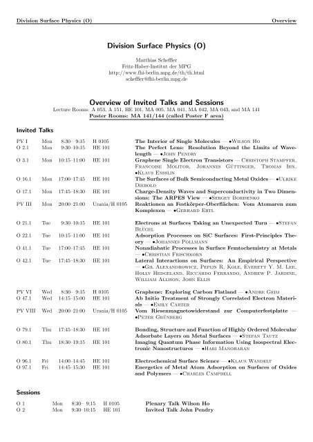
Division Surface Physics (O) Overview<br />
Invited Talks<br />
Division Surface Physics (O)<br />
Matthias Scheffler<br />
Fritz-Haber-Institut der MPG<br />
http://www.fhi-berlin.mpg.de/th/th.html<br />
scheffler@fhi-berlin.mpg.de<br />
Overview <strong>of</strong> Invited Talks and Sessions<br />
Lecture Rooms: A 053, A 151, HE 101, MA 005, MA 041, MA 042, MA 043, and MA 141<br />
Poster Rooms: MA 141/144 (called Poster F area)<br />
PV I Mon 8:30– 9:15 H 0105 The Interior <strong>of</strong> Single Molecules — •Wilson Ho<br />
O 2.1 Mon 9:30–10:15 HE 101 The Perfect Lens: Resolution Beyond <strong>the</strong> Limits <strong>of</strong> Wavelength<br />
— •John Pendry<br />
O 3.1 Mon 10:15–11:00 HE 101 Graphene Single Electron Transistors — Christoph Stampfer,<br />
Francoise Molitor, Johannes Güttinger, Thomas Ihn,<br />
•Klaus Ensslin<br />
O 16.1 Mon 17:00–17:45 HE 101 The Surfaces <strong>of</strong> Bulk Semiconducting Metal Oxides — •Ulrike<br />
Diebold<br />
O 17.1 Mon 17:45–18:30 HE 101 Charge-Density Waves and Superconductivity in Two Dimensions:<br />
The ARPES View — •Sergey Borisenko<br />
PV III Mon 20:00–21:00 Urania/H 0105 Reaktionen an Festkörper-Oberflächen: Vom Atomaren zum<br />
Komplexen — •Gerhard Ertl<br />
O 21.1 Tue 9:30–10:15 HE 101 Electrons at Surfaces Taking an Unexpected Turn — •Stefan<br />
Blügel<br />
O 22.1 Tue 10:15–11:00 HE 101 Adsorption Processes on SiC Surfaces: First-Principles <strong>Theory</strong><br />
— •Johannes Pollmann<br />
O 41.1 Tue 17:00–17:45 HE 101 Nonadiabatic Processes in Surface Femtochemistry at Metals<br />
— •Christian Frischkorn<br />
O 42.1 Tue 17:45–18:30 HE 101 Lateral Interactions on Surfaces: An Empirical Perspective<br />
— •Gil Alexandrowicz, Pepijn R. Kole, Everett Y. M. Lee,<br />
Holly Hedgeland, Riccardo Ferrando, Andrew P. Jardine,<br />
William Allison, John Ellis<br />
PV VI Wed 8:30– 9:15 H 0105 Graphene: Exploring Carbon Flatland — •Andre Geim<br />
O 47.1 Wed 14:15–15:00 HE 101 Ab Initio Treatment <strong>of</strong> Strongly Correlated Electron Materials<br />
— •Emily Carter<br />
PV VIII Wed 20:00–21:00 Urania/H 0105 Vom Riesenmagnetowiderstand zur Computerfestplatte —<br />
•Peter Grünberg<br />
O 79.1 Thu 17:45–18:30 HE 101 Bonding, Structure and Function <strong>of</strong> Highly Ordered Molecular<br />
Adsorbate Layers on Metal Surfaces — •Stefan Tautz<br />
O 80.1 Thu 18:30–19:15 HE 101 Imaging Quantum Phase Information Using Isospectral Electronic<br />
Nanostructures — •Hari Manoharan<br />
O 96.1 Fri 14:00–14:45 HE 101 Electrochemical Surface Science — •Klaus Wandelt<br />
O 97.1 Fri 14:45–15:30 HE 101 Energetics <strong>of</strong> Metal Atom Adsorption on Surfaces <strong>of</strong> Oxides<br />
and Polymers — •Charles Campbell<br />
Sessions<br />
O 1 Mon 8:30– 9:15 H 0105 Plenary Talk Wilson Ho<br />
O 2 Mon 9:30–10:15 HE 101 Invited Talk John Pendry
Division Surface Physics (O) Overview<br />
O 3 Mon 10:15–11:00 HE 101 Invited Talk Klaus Ensslin<br />
O 4.1–4.5 Mon 11:15–12:30 MA 042 Nanostructures at Surfaces<br />
O 5.1–5.6 Mon 11:15–12:45 MA 043 Magnetic Nanostructures<br />
O 6.1–6.7 Mon 11:15–13:00 MA 005 Metal Substrates: Clean Surfaces<br />
O 7.1–7.7 Mon 11:15–13:45 HE 101 Symposium: Atomic Wires at Surfaces I<br />
(Invited Speakers: Franz Himpsel, Hanno Weitering, Han<br />
Woong Yeom)<br />
O 8.1–8.11 Mon 12:00–14:45 MA 041 Metal Substrates: Adsorption <strong>of</strong> Organic/Bio Molecules I<br />
O 9 Mon 13:00–13:45 H 0105 Plenary Talk Sankar Das Sarma<br />
O 10.1–10.14 Mon 13:15–16:45 MA 042 Semiconductor Substrates: Epitaxy and Growth<br />
O 11.1–11.6 Mon 13:30–15:00 MA 043 Time-Resolved Spectroscopy I<br />
O 12.1–12.9 Mon 13:30–16:45 MA 005 Symposium: Size-Selected Clusters at Surfaces I<br />
(Invited Speakers: Karl-Heinz Meiwes-Broer, Heinz<br />
Hövel, Thorsten Bernhardt)<br />
O 13.1–13.10 Mon 14:00–16:30 HE 101 Heterogeneous Catalysis<br />
O 14.1–14.6 Mon 15:15–16:45 MA 043 Surface or Interface Magnetism<br />
O 15.1–15.5 Mon 15:30–16:45 MA 041 Methods: O<strong>the</strong>r Experimental Techniques I<br />
O 16 Mon 17:00–17:45 HE 101 Invited Talk Ulrike Diebold<br />
O 17 Mon 17:45–18:30 HE 101 Invited Talk Sergey Borisenko<br />
O 18.1–18.80 Mon 18:30–19:30 Poster F Poster Session I - MA 141/144 (Atomic Wires;<br />
Size-Selected Clusters; Nanostructures; Metal Substrates:<br />
Clean Surfaces+Adsorption <strong>of</strong> Organic /<br />
Bio Molecules+Solid-Liquid Interfaces+Adsorption <strong>of</strong> O<br />
and/or H; Surface or Interface Magnetism; Oxides and<br />
Insulators: Clean Surfaces)<br />
O 19 Mon 20:00–21:00 Urania/H 0105 Evening Talk Gerhard Ertl<br />
O 20 Tue 8:30– 9:15 H 0105 Plenary Talk James Hudspeth<br />
O 21 Tue 9:30–10:15 HE 101 Invited Talk Stefan Blügel<br />
O 22 Tue 10:15–11:00 HE 101 Invited Talk Johannes Pollmann<br />
O 23 Tue 10:30–13:15 A 151 SYNF: Ferroic Materials and Novel Functionalities I<br />
(FV: MA+O+MM+DF+DS+HL+TT)<br />
O 24 Tue 9:30–10:45 H 0105 SYSA: Tayloring Organic Interfaces: Molecular Structures<br />
and Applications I<br />
(Invited Speaker: Fernando Flores; FV:<br />
DS+CPP+HL+O)<br />
O 25 Tue 10:45–13:00 H 0105 SYSA: Tayloring Organic Interfaces: Molecular Structures<br />
and Applications II (Invited Speakers: Norbert<br />
Koch, Antoine Kahn; FV: DS+CPP+HL+O)<br />
O 26.1–26.5 Tue 11:15–12:30 MA 042 Methods: Electronic Structure <strong>Theory</strong><br />
O 27.1–27.6 Tue 11:15–12:45 MA 043 Time-Resolved Spectroscopy II<br />
O 28.1–28.4 Tue 11:15–13:00 MA 005 Symposium: Size-Selected Clusters at Surfaces II<br />
(Invited Speakers: Steven Buratto, Stefan Vajda,<br />
Matthias Arenz)<br />
O 29.1–29.6 Tue 11:15–13:30 HE 101 Symposium: Surface Spectroscopy on Kondo Systems I<br />
(Invited Speakers: Wolf-Dieter Schneider, Fakher Assaad,<br />
Serguei Molodtsov)<br />
O 30.1–30.8 Tue 12:00–14:00 MA 041 Phenomena at Semiconductor Surfaces<br />
O 31 Tue 13:00–13:45 H 0105 Prize Talk Bernard Barbara (Gentner-Kastler Prize)<br />
O 32.1–32.15 Tue 13:00–16:45 MA 042 Oxides and Insulators: Clean Surfaces<br />
O 33.1–33.7 Tue 13:45–16:15 MA 005 Symposium: Frontiers <strong>of</strong> Surface Sensitive Electron Microscopy<br />
I (Invited Speakers: James Hannon, Raoul van<br />
Gastel, Thomas Schmidt)<br />
O 34.1–34.11 Tue 13:45–16:30 MA 043 Metal Substrates: Adsorption <strong>of</strong> Organic/Bio Molecules<br />
II<br />
O 35.1–35.7 Tue 14:00–16:45 HE 101 Symposium: Atomic Wires at Surfaces II<br />
(Invited Speakers: Erio Tosatti, Serge Lemay, Shuji<br />
Hasegawa)<br />
O 36.1–36.10 Tue 14:15–16:45 MA 041 Surfaces and Films: Forces, Structure and Manipulation
Division Surface Physics (O) Overview<br />
O 37 Tue 14:30–17:30 A 151 SYNF: Ferroic Materials and Novel Functionalities II (Invited<br />
Speakers: Jochen Mannhart, Warren Pickett, Yoshinori<br />
Tokura, Ramamoorthy Ramesh, Agnes Bar<strong>the</strong>lemy,<br />
Evgeny Tsymbal; FV: MA+O+MM+DF+DS+HL+TT)<br />
O 38 Tue 14:30–16:30 H 2013 SYSA: Tayloring Organic Interfaces: Molecular Structures<br />
and Applications III (Invited Speaker: Alberto<br />
Salleo; FV: DS+CPP+HL+O)<br />
O 39 Tue 14:30–20:00 Poster A SYSA: Tayloring Organic Interfaces: Molecular<br />
Structures and Applications IV (Poster; FV:<br />
DS+CPP+HL+O)<br />
O 40 Tue 16:30–18:30 H 2013 SYSA: Tayloring Organic Interfaces: Molecular Structures<br />
and Applications V (Invited speaker: Henning Sirringhaus;<br />
FV: DS+CPP+HL+O)<br />
O 41 Tue 17:00–17:45 HE 101 Invited Talk Christian Frischkorn<br />
O 42 Tue 17:45–18:30 HE 101 Invited Talk Gil Alexandrowicz<br />
O 43.1–43.46 Tue 18:30–19:30 Poster F Poster Session II - MA 141/144 (Surface Spectroscopy<br />
on Kondo Systems; Frontiers <strong>of</strong> Surface Sensitive<br />
Electron Microscopy; Methods: Scanning Probe<br />
Techniques+Electronic Structure <strong>Theory</strong>+O<strong>the</strong>r; Time-<br />
Resolved Spectroscopy <strong>of</strong> Surface Dynamics with EUV<br />
and XUV Radiation; joint by SYNF posters)<br />
O 44 Wed 8:30– 9:15 H 0105 Plenary Talk André Geim<br />
O 45 Wed 9:15–10:00 H 0105 Plenary Talk Knut Urban<br />
O 46 Wed 13:30–14:15 HE 101 Invited Talk Stefan Mayr (Gaede Prize)<br />
O 47 Wed 14:15–15:00 HE 101 Invited Talk Emily Carter<br />
O 48 Wed 14:30–17:30 H 2013 SYSA: Tayloring Organic Interfaces: Molecular Structures<br />
and Applications VI (Invited Speaker: Ivan Stich;<br />
FV: DS+CPP+HL+O)<br />
O 49.1–49.10 Wed 15:15–17:45 MA 005 Particles and Clusters<br />
O 50.1–50.8 Wed 15:15–18:00 HE 101 Symposium: Surface Spectroscopy on Kondo Systems II<br />
(Invited Speakers: Jonathan Denlinger, Johann Kroha,<br />
Alexander Schneider)<br />
O 51.1–51.13 Wed 15:15–18:30 MA 041 Metal Substrates: Adsorption <strong>of</strong> Organic/Bio Molecules<br />
III<br />
O 52.1–52.13 Wed 15:15–18:30 MA 042 Time-Resolved Spectroscopy III<br />
O 53.1–53.13 Wed 15:15–18:30 MA 043 Surface Nanopatterns<br />
O 54 Wed 17:45–19:30 H 2013 SYSA: Tayloring Organic Interfaces: Molecular Structures<br />
and Applications VII (Invited Speaker: Stephan<br />
Roth; FV: DS+CPP+HL+O)<br />
O 55.1–55.77 Wed 18:30–19:30 Poster F Poster Session III - MA 141/144 (Methods: Atomic<br />
and Electronic Structure; Particles and Clusters; Heterogeneous<br />
Catalysis; Semiconductor Substrates: Epitaxy<br />
and Growth+Adsorption+Clean Surfaces+Solid-Liquid<br />
Interfaces; Oxides and Insulators: Solid-Liquid Interfaces+Epitaxy<br />
and Growth; Phase Transitions; Metal<br />
Substrates: Adsorption <strong>of</strong> Inorganic Molecules+Epitaxy<br />
and Growth; Surface Chemical Reactions; Bimetallic<br />
Nanosystems: Tuning Physical and Chemical Properties;<br />
Oxides and insulators: Adsorption; Organic, polymeric,<br />
biomolecular films; etc.)<br />
O 56 Wed 20:00–21:00 Urania/H 0105 Evening Talk Peter Grünberg<br />
O 57 Thu 8:30– 9:15 H 0105 Plenary Talk Helmut Grubmüller<br />
O 58.1–58.4 Thu 9:30–11:00 HE 101 Symposium: Beyond Optical Wavelengths: Time-<br />
Resolved Spectroscopy <strong>of</strong> Surface Dynamics with EUV<br />
and XUV Radiation I (Invited Speakers: Reinhard Kienberger,<br />
Martin Aeschlimann)<br />
O 59.1–59.10 Thu 9:30–12:00 MA 041 Molecular Nanostructures<br />
O 60.1–60.8 Thu 9:30–12:15 MA 005 Symposium: Bimetallic Nanosystems: Tuning Physical<br />
and Chemical Properties I (Invited Speakers: Harald<br />
Brune, Michael Hilgendorff, Konstantin Neyman)
Division Surface Physics (O) Overview<br />
O 61 Thu 9:30–12:30 A 151 SYEC: Exact-Exchange and Hybrid Functionals Meet<br />
Quasiparticle Energy Calculations I (Invited Speakers:<br />
Gustavo Scuseria, Andreas Görling, Georg Kresse, Angel<br />
Rubio, Mark van Schilfgaarde, Michael Rohlfing; FV:<br />
O+HL+DF+TT)<br />
O 62.1–62.12 Thu 9:30–12:30 MA 042 Metal Substrates: Adsorption <strong>of</strong> Inorganic Molecules<br />
O 63.1–63.8 Thu 9:30–12:30 MA 043 Symposium: Frontiers <strong>of</strong> Surface Sensitive Electron Microscopy<br />
II (Invited Speakers: Jürgen Kirschner, Liviu<br />
Chelaru, Michael Bauer, Claus Schneider)<br />
O 64.1–64.6 Thu 11:15–12:45 HE 101 Metal Substrates: Adsorption <strong>of</strong> Organic/Bio Molecules<br />
IV<br />
O 65.1–65.11 Thu 12:00–14:45 MA 141 Methods: <strong>Theory</strong> and Experiment<br />
O 66.1–66.10 Thu 12:45–15:15 MA 041 Metallic Nanostructures I (on Metals)<br />
O 67 Thu 13:00–13:45 H 0105 Prize Talk Fedor Jelezko (Walter Schottky Prize)<br />
O 68.1–68.6 Thu 13:15–14:45 MA 043 Oxides and Insulators: Adsorption I<br />
O 69.1–69.4 Thu 14:00–15:00 MA 042 Symposium: Size-Selected Clusters at Surfaces III<br />
O 70 Thu 14:00–17:00 A 151 SYMS: Modern Developments in Multiphysics Materials<br />
Simulations I (Invited Speakers: David Pettifor, Alessandro<br />
De Vita, Chris Wolverton, Ingo Steinbach, Walter<br />
Thiel, Karsten Reuter; FV: O+HL+MM)<br />
O 71 Thu 14:00–17:00 A 053 SYEC: Exact-Exchange and Hybrid Functionals<br />
Meet Quasiparticle Energy Calculations II (FV:<br />
O+HL+DF+TT)<br />
O 72.1–72.8 Thu 14:00–17:00 HE 101 Symposium: Beyond Optical Wavelengths: Time-<br />
Resolved Spectroscopy <strong>of</strong> Surface Dynamics with EUV<br />
and XUV Radiation II (Invited Speakers: Wilfried Wurth,<br />
Hermann Dürr, Shik Shin)<br />
O 73.1–73.10 Thu 14:00–17:30 MA 005 Symposium: Bimetallic Nanosystems: Tuning Physical<br />
and Chemical Properties II (Invited Speakers: André<br />
Fielicke, Thomas Risse, Jürgen Behm)<br />
O 74.1–74.9 Thu 15:00–17:15 MA 141 Metal Substrates: Adsorption <strong>of</strong> O and/or H<br />
O 75.1–75.8 Thu 15:15–17:15 MA 042 Oxides and Insulators: Epitaxy and Growth<br />
O 76.1–76.9 Thu 15:15–17:30 MA 043 Organic, Polymeric, Biomolecular Films - also with Adsorbates<br />
O 77.1–77.8 Thu 15:30–17:30 MA 041 Methods: Scanning Probe Techniques I<br />
O 78 Thu 17:00–18:30 H 2032 SYSA: Tayloring Organic Interfaces: Molecular Structures<br />
and Applications VIII (Invited Speaker: Tomasz<br />
Kowalewski; FV: DS+CPP+HL+O)<br />
O 79 Thu 17:45–18:30 HE 101 Invited Talk Stefan Tautz<br />
O 80 Thu 18:30–19:15 HE 101 Invited Talk Hari Manoharan<br />
O 81 Thu 18:30–19:30 Poster F Poster Session IV - MA 141/144: SYMS II and SYEC III<br />
(Modern Developments in Multiphysics Materials Simulations;<br />
Exact-Exchange and Hybrid Functionals Meet<br />
Quasiparticle Energy Calculations)<br />
O 82 Thu 19:30–20:00 HE 101 General Meeting <strong>of</strong> <strong>the</strong> Surface Science Division<br />
O 83 Thu 20:00–21:00 HE 101 Post Deadline Session (followed by Surface Science Symposion)<br />
O 84 Fri 8:30– 9:15 H 0105 Plenary Talk Wolfgang Kleemann<br />
O 85 Fri 9:15–10:00 H 0105 Prize Talk Hagen Kleinert (<strong>Max</strong> Born Prize)<br />
O 86.1–86.7 Fri 9:30–11:15 MA 141 Oxides and Insulators: Adsorption II<br />
O 87.1–87.7 Fri 9:30–12:00 HE 101 Symposium: Beyond Optical Wavelengths: Time-<br />
Resolved Spectroscopy <strong>of</strong> Surface Dynamics with EUV<br />
and XUV Radiation III (Invited Speakers: Christian<br />
Spielmann, Matias Bargheer, Philippe Wernet)<br />
O 88.1–88.12 Fri 9:30–12:30 MA 005 Metallic Nanostructures II (on Semiconductors)<br />
O 89.1–89.12 Fri 9:30–12:30 MA 041 Metal Substrates: Epitaxy and Growth<br />
O 90.1–90.7 Fri 10:15–12:00 MA 042 Methods: Scanning Probe Techniques II<br />
O 91 Fri 10:15–12:30 A 151 SYEC: Exact-Exchange and Hybrid Functionals<br />
Meet Quasiparticle Energy Calculations IV (FV:<br />
O+HL+DF+TT)
Division Surface Physics (O) Overview<br />
O 92 Fri 10:15–13:00 A 053 SYMS: Modern Developments in Multiphysics Materials<br />
Simulations III (FV: O+HL+MM)<br />
O 93.1–93.11 Fri 10:15–13:00 MA 043 Surface Chemical Reactions<br />
O 94.1–94.5 Fri 12:00–13:15 MA 141 Methods: O<strong>the</strong>r Experimental Techniques II<br />
O 95 Fri 13:15–14:00 H 0105 Special Talk Theodore Postol<br />
O 96 Fri 14:00–14:45 HE 101 Invited Talk Klaus Wandelt<br />
O 97 Fri 14:45–15:30 HE 101 Invited Talk Charles Campbell<br />
Evening Talks by Nobel Laureates 2007<br />
Monday, 8:00 p.m., Urania Gerhard Ertl<br />
Wednesday, 8:00 p.m., Urania Peter Grünberg<br />
Urania is best reached by subway U1 from Ernst-Reuter-Platz to Wittenbergplatz (just a 4 min. train ride + 8 min. walk).<br />
Both lectures will also be presented in a live broadcast in H 0105.<br />
Annual General Meeting <strong>of</strong> <strong>the</strong> Surface Science Division<br />
Thursday, 7:30 p.m., HE 101<br />
• Report <strong>of</strong> <strong>the</strong> Chairman <strong>of</strong> <strong>the</strong> DPG Surface Science Division<br />
• Miscellaneous<br />
NOTES<br />
Poster Sessions O18 (Monday), O43 (Tuesday), O55 (Wednesday), and O81 (Thursday) at 6:30-7:30 p.m. in MA 141/144<br />
(Poster F area) - Posters should be put up between 10:00 and 11:00 a.m. and must be removed before 10:00 a.m. on <strong>the</strong><br />
following day. The poster presenter should be present at <strong>the</strong> poster between 6:30 and 7:30 p.m.<br />
Post Deadline Session O83 on Thursday, 8:00-9:00 p.m., in HE 101, followed by <strong>the</strong> Surface Science Symposion at<br />
<strong>the</strong> Alte Mensa, Hardenbergstraße 34.<br />
Deadline for submission <strong>of</strong> abstracts is January 11, 2008; Notification on acceptance will be on February 4, 2008. Support<br />
from Elsevier (Surface Science), SPECS toge<strong>the</strong>r with Bestec, Createc Fischer, and Surface Concept, and from IBM is<br />
gratefully acknowledged.
O 1: Plenary Talk Wilson Ho<br />
Monday<br />
Time: Monday 8:30–9:15 Location: H 0105<br />
The Interior <strong>of</strong> Single Molecules<br />
O 2: Invited Talk John Pendry<br />
Time: Monday 9:30–10:15 Location: HE 101<br />
Invited Talk O 2.1 (23) Mon 9:30 HE 101<br />
The Perfect Lens: Resolution Beyond <strong>the</strong> Limits <strong>of</strong> Wavelength<br />
— •John Pendry — Imperial College London<br />
The lens is one <strong>of</strong> <strong>the</strong> most basic tools <strong>of</strong> optics but <strong>the</strong> resolution<br />
achieved is limited, as if <strong>the</strong> wavelength <strong>of</strong> light defined <strong>the</strong> width <strong>of</strong><br />
a pencil used to draw <strong>the</strong> images. This limit intrudes in all kinds <strong>of</strong><br />
ways. For example it defines <strong>the</strong> storage capacity <strong>of</strong> DVDs where <strong>the</strong><br />
laser can only *see* details <strong>of</strong> <strong>the</strong> order <strong>of</strong> <strong>the</strong> wavelength.<br />
Two types <strong>of</strong> light are associated with a luminous object: <strong>the</strong> near<br />
field and <strong>the</strong> far field. True to its name <strong>the</strong> far field escapes from <strong>the</strong><br />
object and is easily captured and manipulated by a lens, but high resolution<br />
details are hidden in <strong>the</strong> near field and remain localised near<br />
O 3: Invited Talk Klaus Ensslin<br />
<strong>the</strong> source and cannot be captured by a conventional lens. The near<br />
field is familiar to surface scientists in <strong>the</strong> form <strong>of</strong> surface plasmons,<br />
for example. To control <strong>the</strong> near field we have developed a new class<br />
<strong>of</strong> materials with properties not found in nature. These new materials<br />
derive <strong>the</strong>ir properties not from <strong>the</strong> atomic and molecular constituents<br />
<strong>of</strong> <strong>the</strong> solid, but from microstructure which can be designed to give a<br />
wide range <strong>of</strong> novel electromagnetic properties.<br />
The lecture will describe <strong>the</strong> new materials and <strong>the</strong> principles behind<br />
<strong>the</strong>m and show how <strong>the</strong>y may be used to control and manipulate<br />
<strong>the</strong> near field. Finally a prescription will be given for a lens whose resolution<br />
is unlimited by wavelength provided that <strong>the</strong> ideal prescription<br />
for <strong>the</strong> constituent materials is met.<br />
Time: Monday 10:15–11:00 Location: HE 101<br />
Invited Talk O 3.1 (11) Mon 10:15 HE 101<br />
Graphene Single Electron Transistors — Christoph Stampfer,<br />
Francoise Molitor, Johannes Güttinger, Thomas Ihn, and<br />
•Klaus Ensslin — Solid State Physics Lab, ETH Zurich, Switzerland<br />
Graphene flakes are patterned into nanostructures using electron beam<br />
lithography and dry etching. A mesoscopic Hall bar is investigated by<br />
O 4: Nanostructures at Surfaces<br />
low-temperature magnetotransport experiments. The potential inside<br />
<strong>the</strong> Hall bar is tuned by graphene side gates. We demonstrate that<br />
<strong>the</strong> carrier density can be tuned over typical lateral distances <strong>of</strong> 90<br />
nm. This way a tunable graphene single electron transistor is realized.<br />
Clear conductance resonances and Coulomb diamonds are resolved at<br />
a temperature <strong>of</strong> T=2 K. We present data for several graphene single<br />
electron transistors and discuss <strong>the</strong> tunability <strong>of</strong> <strong>the</strong> tunnel barriers as<br />
well as <strong>the</strong> overall electronic configuration <strong>of</strong> <strong>the</strong> device.<br />
Time: Monday 11:15–12:30 Location: MA 042<br />
O 4.1 (534) Mon 11:15 MA 042<br />
Dynamic processes in metalorganic networks based on<br />
oligopyridines and copper — •Achim Breitruck 1 , Harry E.<br />
Hoster 1 , Christoph Meier 2 , Ulrich Ziener 2 , and R. Jürgen<br />
Behm 1 — 1 Institute <strong>of</strong> Surface Chemistry and Catalysis, Ulm University,<br />
D-89069 Ulm — 2 Institute <strong>of</strong> Organic Chemistry III, Ulm<br />
University, D-89069 Ulm<br />
We report on <strong>the</strong> dynamics <strong>of</strong> chiral metalorganic networks on <strong>the</strong> basis<br />
<strong>of</strong> Bis-terpyridines (BTP) and copper which were studied by timeresolved<br />
scanning tunneling microscopy (STM). Using highly oriented<br />
pyrolytic graphite (HOPG) as substrate, <strong>the</strong> samples were prepared<br />
by vapor deposition <strong>of</strong> oligopyridines to form a quadratic 2D molecular<br />
network [1] and post-deposition <strong>of</strong> copper under ultra high vacuum<br />
(UHV) conditions. At Cu coverages below phase saturation, we observed<br />
<strong>the</strong> formation <strong>of</strong> an Cu-organic network, consisting <strong>of</strong> copperfree<br />
and copper-containing BTP trimers. At room temperature, this<br />
allows <strong>the</strong> migration <strong>of</strong> Cu atoms within <strong>the</strong> network via a hopping<br />
mechanism from Cu-containing to Cu-free trimers on a timescale <strong>of</strong><br />
seconds. The mechanism is accompanied by a local rearrangement <strong>of</strong><br />
<strong>the</strong> BTP molecules. Despite <strong>the</strong> high adlayer dynamics, we find very<br />
large enantiopure domains with sizes > 10 4 nm 2 .<br />
[1] H.E. Hoster et al., Langmuir 23, 11570-11579, (2007)<br />
[2] A. Breitruck et al., Surf. Sci. 601, 4200-4205, (2007)<br />
O 4.2 (542) Mon 11:30 MA 042<br />
Mid infrared microspectroscopy: Characterization od<br />
diamond-like (DL) and polymer-like (PL) single nanoparticle<br />
— •Jean-Sébastien Samson 1 , Raphaella Weiss 2 , Erik<br />
Bründermann 1 , Jörg Winter 2 , and Martina Havenith 1 —<br />
1 Physical Chemistry 2, Ruhr-University Bochum, Bochum, Germany<br />
— 2 Experimental Physics 1, Ruhr-University Bochum, Bochum, Germany<br />
We report on <strong>the</strong> infrared spectroscopic characterization <strong>of</strong> plasma<br />
nanoparticles formed in a dusty plasma by scanning near-field infrared<br />
microscopy (SNIM). We use high power OPO-lasers with up to 2,7<br />
W output power as radiation source [1] which emit in <strong>the</strong> so-called<br />
fingerprint region (2,5-4 um). We were able to use <strong>the</strong> characteristic<br />
N-H absorption band around 3300 cm-1 to spectrally resolve a shift<br />
<strong>of</strong> <strong>the</strong> band between <strong>the</strong> diamond-like and <strong>the</strong> polymer-like phase.<br />
The measurement were carried out on a sample containing 100 nm<br />
diamond-like and 400 nm polymer-like plasma nanoparticles. Our results<br />
demonstrate <strong>the</strong> high sensitivity <strong>of</strong> SNIM for characterization <strong>of</strong><br />
nanoparticles found in plasma. [1]J.-S. Samson et al. PCCP, (2006),<br />
8, 753-758<br />
O 4.3 (121) Mon 11:45 MA 042<br />
Nanostructuring <strong>of</strong> <strong>the</strong> HOPG surface — •Artur Böttcher 1 ,<br />
Markus Cudaj 1 , Daniel Löffler 1 , Sharali Malik 2 , Manfred<br />
Kappes 1,2 , Patrice Brenner 3 , and Dagmar Gerthsen 3 — 1 Institut<br />
für Physikalische Chemie, Universität Karlsruhe, Karlsruhe, Germany<br />
— 2 Institut für Nanotechnologie, Forschungszentrum Karlsruhe, Germany<br />
— 3 Laboratorium für Elektronenmikroskopie, Universität Karlsruhe,<br />
Germany<br />
By combining <strong>the</strong> focused ion beam technique, 30keV-Ga + -FIB, with<br />
high-temperature oxidation well defined periodic structures were fabricated<br />
on HOPG surfaces [1]. The method exploits <strong>the</strong> high reactivity<br />
<strong>of</strong> <strong>the</strong> amorphous surface areas towards <strong>the</strong> oxidation-induced gasification<br />
<strong>of</strong> undercoordinated carbon sites, C→CO, CO2. Large surface<br />
areas covered by periodically arranged nanocavities, gratings and arrays<br />
<strong>of</strong> nm-sized squares have been fabricated routinely. The minimum
width <strong>of</strong> <strong>the</strong> grooves written is limited by <strong>the</strong> interaction <strong>of</strong> <strong>the</strong> ion<br />
beam with <strong>the</strong> substrate and levels presently <strong>of</strong>f at 80 nm. The mean<br />
depth <strong>of</strong> <strong>the</strong> grooves can be easily varied in <strong>the</strong> range up to 55 nm<br />
by applying different ionic doses. These parameters enable to fabricate<br />
large arrays <strong>of</strong> nanographene plates with desired size and shape.<br />
Two stages are clearly distinguishable in <strong>the</strong> kinetics <strong>of</strong> <strong>the</strong> etching<br />
process: within <strong>the</strong> early stage <strong>the</strong> amorphous carbon is removed and<br />
in <strong>the</strong> later stage <strong>the</strong> prism surfaces <strong>of</strong> <strong>the</strong> regular graphite are gradually<br />
gasified with lower efficiency. The integral removal probability<br />
depends on <strong>the</strong> surface temperature and ranges from 10 −11 to 10 −8<br />
C/O2. [1] A. Böttcher et al. Nanotechnology, 17(2006)<br />
O 4.4 (412) Mon 12:00 MA 042<br />
Effect <strong>of</strong> HF concentration on physical and electronic properties<br />
<strong>of</strong> electrochemical formed nano-porous silicon —<br />
•Pushpendra Kumar 1 , Manash Ghosh 1 , Hongdan Yan 1 , Frank<br />
Ludwig 2 , Meinhard Schilling 2 , and Peter Lemmens 1 — 1 IPKM,<br />
TU-Braunschweig — 2 EMG, TU-Braunschweig<br />
We report on <strong>the</strong> preparation and functionalization <strong>of</strong> porous silicon<br />
(PS) using electrochemical etching in hydr<strong>of</strong>luoric (HF) acid based so-<br />
O 5: Magnetic Nanostructures<br />
Monday<br />
lutions. The properties <strong>of</strong> PS such as thickness <strong>of</strong> <strong>the</strong> porous layer,<br />
porosity and average pore diameter are precisely controlled and characterized<br />
using optical absorption, nitrogen sorption iso<strong>the</strong>rms, field<br />
emission SEM, Raman and PL spectroscopy. Functionalization was<br />
performed by oxidizing and subsequent doping with different dyes and<br />
magnetic molecules.<br />
O 4.5 (413) Mon 12:15 MA 042<br />
Preparation and functionalization <strong>of</strong> porous anodic aluminum<br />
oxide templates — •Hongdan Yan 1 , Seth White 1 , Pushpendra<br />
Kumar 1 , Peter Lemmens 1 , and Pengxiang Zhang 2 — 1 IPKM,TU-<br />
Braunschweig — 2 IAMPE, Kunming University <strong>of</strong> Science and Technology,<br />
Yunnan, China<br />
We report on <strong>the</strong> preparation <strong>of</strong> porous anodic aluminum oxide templates<br />
(AAO) and <strong>the</strong>ir functionalization/modification. AAO with<br />
nanoporous morphology is a well controlled template material due to<br />
<strong>the</strong> high density and uniformity <strong>of</strong> nano pores. Free standing, transparent<br />
membranes have been prepared and doped with dyes, magnetic<br />
molecules. Ni and Fe nano-wires have been grown within <strong>the</strong> pores by<br />
electrodeposition.<br />
Time: Monday 11:15–12:45 Location: MA 043<br />
O 5.1 (666) Mon 11:15 MA 043<br />
Probing <strong>the</strong> surface states <strong>of</strong> single atoms on cobalt nanoislands<br />
— •Laurent Limot 1 , Benjamin Heinrich 1 , Mircea-Vasile<br />
Rastei 1 , Cristian Iacovita 1 , Pavel A. Ignatiev 2 , Valeri S.<br />
Stepanyuk 2 , Patrick Bruno 2 , and Jean-Pierre Bucher 1 —<br />
1 Institut de Physique et Chimie des Matériaux de Strasbourg, UMR<br />
7504, Université Louis Pasteur, F-67034 Strasbourg, France — 2 <strong>Max</strong>-<br />
<strong>Planck</strong>-Institut für Mikrostrukturphysik, D-06120 Halle/Saale, Germany<br />
With <strong>the</strong> remarkable downscaling <strong>of</strong> data-storage bits, both writing<br />
and reading processes become extremely challenging, since read sensors<br />
need to be comparable to <strong>the</strong> bit size, and at <strong>the</strong> same time, <strong>the</strong>ir<br />
sensitivity must be improved due to <strong>the</strong> loss in signal-to-noise ratio.<br />
Future progress strongly relies on our fundamental understanding <strong>of</strong><br />
magnetic phenomena in reduced dimensions.<br />
Atoms on magnetic nanoislands represent a model playground for investigating<br />
such phenomena. In this study, we focus on <strong>the</strong> electronic<br />
properties <strong>of</strong> single Ni, Cu and Co atoms adsorbed on cobalt nanoislands<br />
grown on <strong>the</strong> Cu(111) surface. By combining low-temperature<br />
scanning tunneling spectroscopy with ab initio calculations we reveal<br />
<strong>the</strong> existence <strong>of</strong> a common electronic resonance, resulting from <strong>the</strong> localization<br />
<strong>of</strong> <strong>the</strong> nanoisland surface states at <strong>the</strong> adsorption site <strong>of</strong> <strong>the</strong><br />
atoms.<br />
O 5.2 (537) Mon 11:30 MA 043<br />
Tailoring exchange interactions between magnetic adatoms in<br />
engeneered nanostructures: ab initio study — •Pavel A. Ignatiev,<br />
Valeri S. Stepanyuk, and Patrick Bruno — <strong>Max</strong>-<strong>Planck</strong>-<br />
Institut für Mikrostrukturphysik, Weinberg 2, D-06120 Halle, Germany<br />
The controllable modification <strong>of</strong> quantum states in 1D nanostructures<br />
could permit one to manipulate <strong>the</strong>ir electronic and magnetic properties.<br />
An advanced experimental methods, such as <strong>the</strong> scanning tunneling<br />
microscope (STM), allows one to construct chains on surfaces in<br />
atom-by-atom fashion [1,2]. Our ab initio calculations unambiguously<br />
demonstrate that both sign and magnitude <strong>of</strong> <strong>the</strong> exchange interaction<br />
between magnetic impurities incorporated in nonmagnetic chains<br />
on metal surfaces can be tailored by an appropriate design <strong>of</strong> <strong>the</strong> chain<br />
length and composition [3]. Such engineered 1D systems are experimentally<br />
feasible [4], and <strong>the</strong> above effects should be detectable with<br />
modern technology, for instance, by probing <strong>the</strong> Kondo resonance [5].<br />
[1] S. Folsch, P. Hyldgaard, R. Koch, and K. H. Ploog Phys. Rev.<br />
Lett. 92, 056803 (2004).<br />
[2] N. Nilius T. M. Wallis, and W. Ho, Science 297, 1853 (2002).<br />
[3] P. A. Ignatiev, V. S. Stepanyuk and P. Bruno, submitted to PRL<br />
[4] J. Lagoute, C. Nacci, and S. Folsch Phys. Rev. Lett. 98, 146804<br />
(2007).<br />
[5] P. Wahl, P. Simon, L. Diekhoner, V. S. Stepanyuk, P. Bruno, M.<br />
A. Schneider, and K. Kern, Phys. Rev. Lett. 98, 056601 (2007).<br />
O 5.3 (683) Mon 11:45 MA 043<br />
Ab initio Study <strong>of</strong> Spin-polarized Bound States in Magnetic<br />
Dimers on Metal Surfaces — •Oleg O. Brovko, Valeri S. Stepanyuk,<br />
and Patrick Bruno — <strong>Max</strong>-<strong>Planck</strong>-Institut für Mikrostrukturphysik,<br />
Weinberg 2, D-06120 Halle, Germany<br />
Interaction <strong>of</strong> single adatoms with surface state electrons has been<br />
shown to produce a bound state below <strong>the</strong> surface state band bottom<br />
[1,2]. Similar states have been revealed at nonmagnetic Cu chains<br />
[2]. Using ab initio KKR Green’s function method we study <strong>the</strong> spinpolarized<br />
bound state arising at magnetic dimers on noble metal surfaces.<br />
We demonstrate that <strong>the</strong> spin-splitting <strong>of</strong> <strong>the</strong> bound state can<br />
be utilized to determine <strong>the</strong> exchange coupling <strong>of</strong> a magnetic dimer.<br />
[1] L. Limot, E. Pehlke, J. Kröger, and R. Berndt, Phys. Rev. Lett.<br />
94, 036805 (2005). [2] V. S. Stepanyuk, A. N. Klavsyuk, L. Niebergall,<br />
and P. Bruno, Phys. Rev. B 72, 153407 (2005)<br />
O 5.4 (637) Mon 12:00 MA 043<br />
Quantum resonators on metal surfaces: <strong>the</strong>oretical and experimental<br />
studies — •L. Niebergall 1 , N.N. Negulyaev 2 , V.S.<br />
Stepanyuk 1 , P. Bruno 1 , J. Repp 3 , G. Meyer 4 , and K.-H. Rieder 5<br />
— 1 <strong>Max</strong> <strong>Planck</strong> Institute <strong>of</strong> Microstructure Physics, 06120 Halle,<br />
Germany — 2 Physics <strong>Department</strong>, Martin-Lu<strong>the</strong>r-University Halle-<br />
Wittenberg, 06099 Halle, Germany — 3 Institute <strong>of</strong> Experimental and<br />
Applied Physics, University Regensburg, 93053 Regensburg, Germany<br />
— 4 IBM Research, Zurich Research Laboratory, 8803 Rueschlikon,<br />
Switzerland — 5 Institute <strong>of</strong> Experimental Physics, FU Berlin, 14195<br />
Berlin, Germany<br />
Confinement <strong>of</strong> surface-state electrons on metal surfaces can lead to<br />
many interesting effects [1-3]. Here, we present a combined experimental<br />
and <strong>the</strong>oretical studies on adatom motion in quantum resonators.<br />
Using STM technique we construct two parallel monatomic Cu chains<br />
on Cu(111). Quantum confinement <strong>of</strong> surface electrons between chains<br />
is revealed. Experimental and <strong>the</strong>oretical studies demonstrate that<br />
adatom motion inside <strong>the</strong> resonators at low temperature is determined<br />
by quantized electronic states in resonators.<br />
1. V.S. Stepanyuk et al., Phys. Rev. Lett. 94, 187201 (2005).<br />
2. L. Niebergall et al., Phys. Rev. Lett. 96, 127204 (2006).<br />
3. V.S. Stepanyuk et al., New J. Phys. 9, 388 (2007).<br />
O 5.5 (238) Mon 12:15 MA 043<br />
Self-organized surface ripples as a source <strong>of</strong> magnetic<br />
anisotropies — •J. Fassbender 1 , M. O. Liedke 1 , A. Keller 1 , S.<br />
Facsko 1 , D. Marko 1 , A. Hanisch 1 , J. Grenzer 1 , E. Cizmar 2 , and<br />
S. Zvyagin 2 — 1 Forschungszentrum Dresden-Rossendorf, Institute <strong>of</strong><br />
Ion Beam Physics and Materials Research, Bautzner Landstrasse 128,<br />
01328 Dresden, Germany — 2 Forschungszentrum Dresden-Rossendorf,<br />
High Magnetic Field Laboratory, Bautzner Landstrasse 128, 01328<br />
Dresden, Germany<br />
In thin film magnetism surface and interface morphologies are impor-
tant sources <strong>of</strong> magnetic anisotropy. This can be ei<strong>the</strong>r due to <strong>the</strong> reduced<br />
coordination <strong>of</strong> step edge atoms (intrinsic contribution) or due<br />
to magnetic stray fields emanating from <strong>the</strong> film corrugation (extrinsic<br />
contribution). Low energy ion erosion is perfectly suited to create a<br />
periodic surface modulation (so-called ripples) on <strong>the</strong> nanoscale. By<br />
changing <strong>the</strong> primary energy <strong>of</strong> <strong>the</strong> ions <strong>the</strong> ripple periodicities can<br />
be varied from 20 to 150 nm. Subsequently, thin magnetic films are<br />
deposited on <strong>the</strong>se template systems in order to investigate <strong>the</strong> influence<br />
<strong>of</strong> <strong>the</strong> surface morphology on <strong>the</strong> induced magnetic anisotropies.<br />
For small ripple periodicities a strong uniaxial magnetic anisotropy is<br />
found which rapidly decrease for larger ripple periodicities. In <strong>the</strong> case<br />
<strong>of</strong> Permalloy (Ni81Fe19) <strong>the</strong> induced anisotropy can be more than a<br />
factor <strong>of</strong> 20 larger compared to <strong>the</strong> intrinsic anisotropy <strong>of</strong> flat Permalloy.<br />
The microscopic origin <strong>of</strong> this effect will be discussed.<br />
O 5.6 (447) Mon 12:30 MA 043<br />
Magneto-optical study <strong>of</strong> hexagonal hole arrays in thin magnetic<br />
films — •Georgios Ctistis 1 , Evangelos Papaioannou 2 ,<br />
O 6: Metal Substrates: Clean Surfaces<br />
Monday<br />
Piotr Patoka 1 , Paul Fumagalli 2 , and Michael Giersig 1 —<br />
1 Nanoparticle Technology <strong>Department</strong>, Center <strong>of</strong> Advanced European<br />
Studies and Research, 53175 Bonn, Germany — 2 Institut für Experimentalphysik,<br />
Freie Universität Berlin, 14195 Berlin, Germany<br />
Nanostructured surfaces <strong>of</strong> optically thin films exhibit interesting optical<br />
properties as plasmon assisted transmission and are thus interesting<br />
for opto-electronic applications. Using magnetic materials such as Fe<br />
or Co instead, could result in tailoring <strong>the</strong> magnetic properties <strong>of</strong> <strong>the</strong><br />
materials at desired frequencies.<br />
In this study we present our magneto-optical studies <strong>of</strong> hexagonal<br />
nano-hole arrays <strong>of</strong> 100 nm thick magnetic films (Fe, Co, Ni). Different<br />
meshes were used with hole diameters ranging between 220 nm and<br />
330 nm, while <strong>the</strong> inter-hole distance was kept constant at 470 nm, respectively.<br />
Spectra were taken with a Kerr-spectrometer in <strong>the</strong> range<br />
<strong>of</strong> 0.8 - 5 eV. A strong change in <strong>the</strong> response depending on <strong>the</strong> hole<br />
geometry compared to <strong>the</strong> corresponding closed films is observed. Fur<strong>the</strong>rmore,<br />
recorded hysteresis loops reveal <strong>the</strong> magnetization process<br />
as a function <strong>of</strong> <strong>the</strong> underlying geometry.<br />
Time: Monday 11:15–13:00 Location: MA 005<br />
O 6.1 (25) Mon 11:15 MA 005<br />
Imaging phonon excitation with atomic resolution — •Heiko<br />
Gawronski and Karina Morgenstern — Institute <strong>of</strong> Solid State<br />
Physics, <strong>Department</strong> <strong>of</strong> Surface Science, Leibniz University Hannover,<br />
Appelstr. 2, D-30167 Hannover, Germany<br />
Scanning tunneling microscopy (STM), inelastic tunneling spectroscopy<br />
(IETS), and d 2 I/dV 2 -mapping at low temperature are used to<br />
investigate vibrations <strong>of</strong> Au(111) and Cu(111). The low energy peaks<br />
in <strong>the</strong> IET-spectra at 9 meV on Au(111) and 21 meV on Cu(111) are<br />
attributed to phonons at surfaces. This phonon energy on Au(111) is<br />
not influenced by <strong>the</strong> different stacking <strong>of</strong> <strong>the</strong> surface atoms, but it is<br />
considerably influenced by different atomic distances within <strong>the</strong> surface<br />
layer. In addition, <strong>the</strong> spatial variation <strong>of</strong> <strong>the</strong> phonon excitation<br />
is measured in d 2 I/dV 2 -maps on Au(111). These display a novel type<br />
<strong>of</strong> atomic resolution that is explained in terms <strong>of</strong> site specific phonon<br />
excitation probabilities.<br />
O 6.2 (36) Mon 11:30 MA 005<br />
Diffraction and crystal symmetry in electron pair emission<br />
from surfaces — •Frank O. Schumann, Carsten Winkler, and<br />
Jürgen Kirschner — <strong>Max</strong>-<strong>Planck</strong>-Institut f\”{u}r Mikrostrukturphysik,<br />
Weinberg 2 , 06120 Halle, Germany<br />
We have investigated <strong>the</strong> electron pair emission from a Cu(111) surface<br />
excited with a primary electron beam <strong>of</strong> 30.7 eV kinetic energy via a<br />
coincidence time-<strong>of</strong>-flight experiment. The movement <strong>of</strong> two interacting<br />
particles can be described within <strong>the</strong> so-called two-body problem,<br />
where it is shown that <strong>the</strong> motion <strong>of</strong> <strong>the</strong> center-<strong>of</strong>-mass can be separated<br />
from <strong>the</strong> relative motion. We adopt this notation in our presentation<br />
<strong>of</strong> <strong>the</strong> data. If we focus on <strong>the</strong> motion <strong>of</strong> <strong>the</strong> center-<strong>of</strong>-mass, we<br />
compute <strong>the</strong> sum <strong>of</strong> <strong>the</strong> in-plane momentum <strong>of</strong> <strong>the</strong> pair. Plotting <strong>the</strong><br />
coincidence intensity as a function <strong>of</strong> <strong>the</strong> sum momentum gives a twodimensional<br />
distribution, which displays intensity peaks, if a reciprocal<br />
lattice vector is added to <strong>the</strong> sum momentum <strong>of</strong> this electron pair and<br />
not to <strong>the</strong> individual electrons. This highlights <strong>the</strong> fact that <strong>the</strong> pair<br />
as <strong>the</strong> whole experiences diffraction at <strong>the</strong> surface. This in turn means<br />
that <strong>the</strong> electrons must be interacting. The interaction within <strong>the</strong> pair<br />
is described by <strong>the</strong> relative motion. The intensity distribution <strong>of</strong> this<br />
motion reveals <strong>the</strong> six-fold symmetry <strong>of</strong> <strong>the</strong> surface. Both features are<br />
only observed, if <strong>the</strong> valence band electron comes from <strong>the</strong> vicinity <strong>of</strong><br />
<strong>the</strong> Fermi level, where <strong>the</strong> Cu(111) surface exhibits a Shockley surface<br />
state. For an explanation <strong>of</strong> our observations this electronic state is<br />
important.<br />
O 6.3 (156) Mon 11:45 MA 005<br />
Relaxations at <strong>the</strong> Ag(001) surface: A LEED study<br />
— •Michael Huth, Wolfram Münchgesang, Karl-Michael<br />
Schindler, and Wolf Widdra — Martin-Lu<strong>the</strong>r Universität Halle-<br />
Wittenberg, Institut für Physik, Halle, Deutschland<br />
For low-energy electron diffraction a new approach <strong>of</strong> data recording<br />
and postprocessing has been developed. The improved I(V) curves for<br />
Ag(001) show low intensity features and additional fine structure <strong>of</strong><br />
high intensity peaks. By comparing experimental and calculated I(V)<br />
curves significant relaxations <strong>of</strong> <strong>the</strong> top two layer distances have been<br />
determined. The relaxations found basically confirm recent <strong>the</strong>oretical<br />
predictions [1]. Detailed analysis shows that I(V) curves exhibit<br />
a strong dependence on <strong>the</strong> angle <strong>of</strong> incidence and show that small<br />
deviations from normal incidence can remove essential structures from<br />
<strong>the</strong> I(V) curves.<br />
[1] J.-M. Zhang, Y. Shu, K.-W. Xu, Sol. Stat. Comm. 137 (2006)<br />
441<br />
O 6.4 (644) Mon 12:00 MA 005<br />
How Au(100) and Pt(100) reorganize <strong>the</strong>mselves: Largescale<br />
surface reconstructions studied by all-electron DFT —<br />
•Paula Havu 1 , Ville Havu 1 , Patrick Rinke 1,2 , Volker Blum 1 , and<br />
Matthias Scheffler 1,2 — 1 Fritz-Haber-Institut, Berlin, Germany —<br />
2 University <strong>of</strong> California at Santa Barbara, CA 93106, USA<br />
Pt(100) and Au(100) show large-scale quasi-hexagonal, <strong>of</strong>ten called<br />
(5×20), surface reconstructions that are intimately linked to <strong>the</strong> external<br />
surface conditions (temperature, absorbates, electrochemistry).<br />
The reconstruction energy <strong>of</strong> Pt(100) is known from a careful calorimetric<br />
measurement [1], but earlier first principles studies <strong>of</strong> both surfaces<br />
have so far so far restricted to simpler (5×1) models that neglect<br />
<strong>the</strong> long range aspect <strong>of</strong> <strong>the</strong> reconstruction. We here use <strong>the</strong> new numerical<br />
atom centered orbital based all-electron code <strong>FHI</strong>-aims [2] to<br />
determine <strong>the</strong> full (5×20)-reconstructed surface structure, by means <strong>of</strong><br />
density functional <strong>the</strong>ory (DFT) calcluations. We compare our results<br />
to full-potential LAPW results for older (5×1) models. The full surface<br />
reconstruction is investigated both in DFT-LDA and -GGA (PBE functional),<br />
both to uncover <strong>the</strong> precise relaxation mechanism, and to compare<br />
quantitatively to <strong>the</strong> experimental reconstruction energy. [1] Y.<br />
Y. Yeo, C. E. Wartnaby, D. A. King, Science 268, 1731-1732 (1995). [2]<br />
V. Blum et al., The <strong>FHI</strong>-aims project, www.fhi-berlin.mpg.de/aims/<br />
O 6.5 (388) Mon 12:15 MA 005<br />
determination <strong>of</strong> <strong>the</strong> DOS in Nb(110) from scanning tunneling<br />
spectroscopy — •Stefania C. Bobaru, Berndt Koslowski,<br />
and Paul Ziemann — Institut für Festkörperphysik, Universität Ulm,<br />
D-89069 Ulm, Germany<br />
We investigate <strong>the</strong> electronic structure <strong>of</strong> Nb(110)/Al2O3(0001) by<br />
means <strong>of</strong> Scanning Tunneling Spectroscopy (STS) at 6.2 K. To enable<br />
a comprehensive analysis <strong>of</strong> <strong>the</strong> local electronic structure <strong>of</strong> niobium,<br />
we employ standard I-V as well as I-z and dI/dz-z spectroscopy. The<br />
experimental results will be discussed in <strong>the</strong> framework <strong>of</strong> a recently<br />
developed method for recovering <strong>the</strong> electronic density <strong>of</strong> states (DOS)<br />
from STS data [1]. Based on <strong>the</strong> one-dimensional WKB approximation<br />
this method should enable recovering <strong>the</strong> DOS <strong>of</strong> <strong>the</strong> sample semiquantitatively,<br />
and it should allow principally a deconvolution <strong>of</strong> tip<br />
and sample DOS. In this contribution we first elucidate <strong>the</strong> effect <strong>of</strong><br />
data evaluation on <strong>the</strong> recovered DOS separating contributions from<br />
<strong>the</strong> bulk and <strong>the</strong> surface. We <strong>the</strong>n try to deconvolute <strong>the</strong> DOS <strong>of</strong> tip<br />
and sample at least partially by comparing I-V data and differential
arrier measurements taken at different locations <strong>of</strong> <strong>the</strong> sample with<br />
<strong>the</strong> same tunneling tip.<br />
References:<br />
[1] B. Koslowski, Ch. Dietrich, A. Tschetschetkin, P. Ziemann,<br />
Phys.Rev. B 75, 035421 (2007).<br />
O 6.6 (307) Mon 12:30 MA 005<br />
Surface electronic structure <strong>of</strong> Y(0001): A consistent picture<br />
— •Michael Budke, Juliet Correa, and Markus Donath<br />
— Physikalisches Institut, WWU Münster, Wilhelm-Klemm-Str. 10,<br />
48149 Münster<br />
The photoemission (UPS) spectra <strong>of</strong> <strong>the</strong> (0001) surfaces <strong>of</strong> rare earth<br />
single crystals like Sc, Pr, Y, Gd, Tb, Ho and Er show an intense feature<br />
at about 10 eV binding energy. Its sensitivity to <strong>the</strong> degree <strong>of</strong> surface<br />
order led to <strong>the</strong> acronym “surface order dependent state”(SODS)<br />
in <strong>the</strong> literature [1]. For more than 20 years it remains an unsolved<br />
puzzle why <strong>the</strong> SODS was not observed in photoemission data obtained<br />
from clean rare-earth thin films grown on W(110) or Mo(110).<br />
On <strong>the</strong> one hand, experiments performed on rare earth single crystals<br />
are known to suffer from inherent impurities. On <strong>the</strong> o<strong>the</strong>r hand,<br />
thin films grown on W(110) or Mo(110) are <strong>of</strong> higher purity but not<br />
as well ordered as single crystals due to <strong>the</strong> considerable lattice mismatch<br />
between substrate and film. In our contribution, we give a<br />
consistent picture <strong>of</strong> <strong>the</strong> surface electronic structure <strong>of</strong> Y(0001) that<br />
explains <strong>the</strong> differences between single-crystal and thin-film UPS data.<br />
Fur<strong>the</strong>rmore, we provide evidence that <strong>the</strong> SODS is in fact due to car-<br />
Monday<br />
bon contamination, and not, as believed for more than 20 years, an<br />
indicator for a well prepared, highly ordered surface.<br />
[1] S.D. Barrett, Surface Science Reports 14, 271 (1992).<br />
O 6.7 (501) Mon 12:45 MA 005<br />
Efficient ab-initio based modelling <strong>of</strong> segregation pr<strong>of</strong>iles in<br />
metal alloys for arbitrary bulk concentrations — •Tobias Kerscher<br />
and Stefan Müller — Lehrstuhl für Festkörperphysik, Universität<br />
Erlangen-Nürnberg, Staudtstr. 7, D-91058 Erlangen<br />
As shown recently [1], <strong>the</strong> combination <strong>of</strong> density functional <strong>the</strong>ory<br />
(DFT) with cluster expansion methods and Monte-Carlo simulations<br />
is a powerful tool to model surface segregation in binary metal alloys.<br />
However, <strong>the</strong> predicted surface properties are <strong>the</strong>n restricted to <strong>the</strong> inplane<br />
lattice parameter defined by <strong>the</strong> bulk concentration <strong>of</strong> <strong>the</strong> alloy.<br />
Indeed, a change <strong>of</strong> <strong>the</strong> bulk concentration demands <strong>the</strong> re-calculation<br />
<strong>of</strong> all atomic configurations via DFT being <strong>the</strong> most time-consuming<br />
factor in <strong>the</strong> used approach. We will present a cluster-expansion Hamiltonian<br />
which provides universal and volume-corrected bulk energetics<br />
for all bulk concentrations, and simultaneously, minimizes <strong>the</strong> number<br />
<strong>of</strong> DFT calculation which have to be performed. This is demonstrated<br />
for <strong>the</strong> [100] direction <strong>of</strong> <strong>the</strong> bulk systems Pt25Rh75 and Pt50Rh50.<br />
Our results are in quantitative agreement with experimental measurements.<br />
Supported by Deutsche Forschungs-Gemeinschaft<br />
[1] S. Müller, M. Stöhr, O. Wieckhorst, Appl. Phys. A. 82, 415<br />
(2006).<br />
O 7: Symposium: Atomic Wires at Surfaces I<br />
(Invited Speakers: Franz Himpsel, Hanno Weitering, Han Woong Yeom)<br />
Time: Monday 11:15–13:45 Location: HE 101<br />
O 7.1 (105) Mon 11:15 HE 101<br />
Low-Dimensional Electrons at Metallic Semiconductor Surfaces<br />
— •Franz Himpsel — Dept. Physics, University <strong>of</strong> Wisconsin,<br />
Madison, USA<br />
In recent years, it has become possible to create well-ordered semiconductor<br />
surfaces with metallic surface states by using self-assembly<br />
<strong>of</strong> metal atoms. Since <strong>the</strong>se states lie in <strong>the</strong> band gap <strong>of</strong> <strong>the</strong> semiconductor,<br />
<strong>the</strong>y completely de-couple from <strong>the</strong> substrate. The surface<br />
structures can be tailored from two-dimensional triangular lattices to<br />
nearly one-dimensional atomic chains, which may be considered as<br />
<strong>the</strong> ultimate nanowires. The dimensionality can be varied systematically<br />
between 2D and 1D by using vicinal surfaces with variable step<br />
spacing. Angle-resolved photoemission and scanning tunneling spectroscopy<br />
reveal surprising features, such as a fractional band filling,<br />
nanoscale phase separation into doped and undoped chain segments,<br />
and a spin-splitting at a non-magnetic surface.<br />
O 7.2 (681) Mon 11:45 HE 101<br />
Properties and origin <strong>of</strong> one-dimensional Au nanostructures<br />
on tungsten surface carbides — •Andrei Varykhalov, Oliver<br />
Rader, and Wolfgang Gudat — BESSY Berlin<br />
We introduce a universal template for one-dimensional selforganization.<br />
The tungsten surface carbide W(110)/C-R(15×3) displays<br />
a large-scale reconstruction with interesting properties [1,2]. We<br />
recently showed that this structure which is rotated by 14 ◦ relative<br />
to W is able to order various atomic species ranging from C60 superclusters<br />
which show ”magic” numbers to Au films which become patterned<br />
in a way that <strong>the</strong>y in turn serve as templates for needle-shaped<br />
Ni clusters [3]. The Au reconstruction is uniaxial with corresponding<br />
one-dimensional E(k) dispersion [3]. We will demonstrate <strong>the</strong> origin <strong>of</strong><br />
<strong>the</strong> self-organization <strong>of</strong> Au comparing (15×12) and (15×3) templates<br />
by STM and LEED. Two principally different mechanisms are identified:<br />
At room temperature, regular Au clusters develop which are 1<br />
monolayer high when grown on <strong>the</strong> (15×12) structure and 2 monolayers<br />
high on (15×3) but always aligned along <strong>the</strong> physical potential<br />
<strong>of</strong> <strong>the</strong> carbide nanomesh, i. e., <strong>of</strong>f by 14 ◦ . Annealing rearranges <strong>the</strong><br />
Au adatoms towards a nanowire-like reconstruction which has rotated<br />
back to <strong>the</strong> [001] <strong>of</strong> W. The chemical driving force for this is revealed<br />
in detail by photoemission spectra from <strong>the</strong> valence band and <strong>the</strong> W4f<br />
core level.<br />
[1] M. Bode et al., Surf. Sci. 344, 185 (1995). [2] A. Varykhalov et<br />
al., Phys. Rev. B 72, 115440 (2005). [3] A. Varykhalov et al., Phys.<br />
Rev. B 73, 241404(R) (2006); 74, 95420 (2006); 72, 241404(R) (2005).<br />
O 7.3 (5) Mon 12:00 HE 101<br />
Spatial Mapping <strong>of</strong> <strong>the</strong> Electronic States <strong>of</strong> a One-<br />
Dimensional System — Arie van Houselt, Bene Poelsema, and<br />
•Harold Zandvliet — University <strong>of</strong> Twente, Enschede, The Ne<strong>the</strong>rlands<br />
Using low-temperature scanning tunneling microscopy and spectroscopy<br />
we have recorded spatial maps <strong>of</strong> confined electronic states in<br />
<strong>the</strong> troughs between self-organized Pt nanowires on Ge(001) that are<br />
spaced 2.4 nm apart. Two subbands are resolved, which correspond to<br />
<strong>the</strong> lowest energy levels <strong>of</strong> a quantum mechanical particle in a box. As<br />
expected, <strong>the</strong> spatial dI/dV maps exhibit a maximum and a minimum<br />
in <strong>the</strong> middle <strong>of</strong> <strong>the</strong> troughs for <strong>the</strong> n=1 and n=2 states, respectively.<br />
O 7.4 (561) Mon 12:15 HE 101<br />
Electrons Confined to Atomic Nanowires <strong>of</strong> Au on Ge(001) —<br />
•Jörg Schäfer, Christian Blumenstein, Sebastian Meyer, Marc<br />
Wisniewski, and Ralph Claessen — Physikalisches Institut, Universität<br />
Würzburg, D-97074 Würzburg<br />
Nanowires reach <strong>the</strong>ir lower size limit in metal-induced chains on semiconductors.<br />
In such quasi-one-dimensional (1D) systems, <strong>the</strong> Fermi<br />
surface may host a charge density wave (CDW) with concomitant energy<br />
gaps. Metallic chain reconstructions on Ge(001) can serve as<br />
model systems, such as Au nanowires on Ge(001). In using scanning<br />
tunneling microscopy, one finds that <strong>the</strong> wires are spaced by several<br />
Ge lattice constants, with <strong>the</strong>ir electron density being laterally strictly<br />
confined. In <strong>the</strong> related system Pt/Ge(001), our data show a conduction<br />
path <strong>of</strong> atomic dimensions [1], yet various dimer elements are<br />
detected. In contrast, in Au nanowires <strong>the</strong> charge density is spread<br />
out very evenly in chain direction, as seen for a large range <strong>of</strong> bias values.<br />
This reflects an unusually pronounced delocalization with metallic<br />
character at room temperature. Most significantly, at low temperature<br />
indication <strong>of</strong> a periodic superstructure along <strong>the</strong> chains <strong>of</strong> twice <strong>the</strong><br />
unit cell is found. The electronic properties have also been explored<br />
with angle-resolved photoemission. These measurements reveal freeelectron-like<br />
bands close to <strong>the</strong> Fermi level. Moreover, <strong>the</strong> observed<br />
Fermi level crossings are supportive <strong>of</strong> a CDW nesting condition. The<br />
talk will review <strong>the</strong> various aspects <strong>of</strong> this exceptional 1D electron liquid,<br />
and present a perspective regarding related systems.<br />
[1] J. Schäfer et al., Phys. Rev. B 74, 041404(R) (2006).
O 7.5 (31) Mon 12:30 HE 101<br />
Electronic instabilities and fluctuations in quantum chains —<br />
•Hanno H. Weitering — <strong>Department</strong> <strong>of</strong> Physics and Astronomy, The<br />
University <strong>of</strong> Tennessee, Knoxville, TN 37931, USA — Materials Science<br />
and Technology Division, Oak Ridge National Laboratory, Oak<br />
Ridge, TN 37831, USA<br />
One-dimensional (1D) quantum conductors have always captured <strong>the</strong><br />
imagination <strong>of</strong> physicists. While a strictly 1D material remains a <strong>the</strong>oretical<br />
construct, a vast number <strong>of</strong> materials can be viewed as macroscopic<br />
ensembles <strong>of</strong> weakly-coupled quantum chains, making <strong>the</strong>m interesting<br />
test cases for <strong>the</strong>oretical predictions. I will discuss <strong>the</strong> electronic<br />
and magnetic properties <strong>of</strong> some quasi 1D systems on Si and Ge<br />
surfaces. Highlights include <strong>the</strong> remarkable self-assembly <strong>of</strong> rare-earth<br />
metal atoms on Si into silicide nanowires. Large strain anisotropy<br />
in <strong>the</strong>se wires can lead to extraordinary aspect ratios and uniformity.<br />
The thinnest wires exhibit electronic properties reminiscent <strong>of</strong> a multichannel<br />
1D conductor. These include <strong>the</strong> stepwise increase <strong>of</strong> <strong>the</strong> tunnel<br />
current as a function <strong>of</strong> tip bias in scanning tunneling microscopy,<br />
and <strong>the</strong> appearance <strong>of</strong> a fluctuating charge density wave or Peierls<br />
instability at low temperature. Peierls instabilities are normally attributed<br />
to a collective screening response <strong>of</strong> <strong>the</strong> 1D electron gas,<br />
but in <strong>the</strong> present case <strong>the</strong>re is no obvious connection to <strong>the</strong> classical<br />
Peierls picture. The remarkable assembly <strong>of</strong> yttrium atoms into long<br />
nanowires with built-in metal/semiconductor junctions is illustrative<br />
<strong>of</strong> how <strong>the</strong> finite-size- and temperature-scaling behavior <strong>of</strong> a collective<br />
phenomenon may one day be exploited in nano-architectures.<br />
O 7.6 (33) Mon 13:00 HE 101<br />
Phase transitions and fluctuations <strong>of</strong> metallic atomic wires on<br />
silicon — •Han Woong Yeom — CAWL, Yonsei University, Seoul,<br />
Korea<br />
Wire-type metals in nano scale are essential for nano/molecular electronics<br />
and <strong>the</strong>ir fundamental properties are challenging with vari-<br />
Monday<br />
ous exotic ground states and fluctuations. As an unconventional form<br />
<strong>of</strong> such 1D metallic systems, we have investigated <strong>the</strong> self-organized<br />
metallic atomic wires on flat and vicinal Si surfaces such as In/Si(111)<br />
[1, 2, 3], Au/Si(111) [4], Au/Si(557) [5], and Au/Si(553) [6], and<br />
Pb/Si(557) [7]. For some <strong>of</strong> <strong>the</strong>se systems, we observed Peierls-type<br />
phase transitions due to <strong>the</strong> 1D bands nested fully with electron fillings<br />
<strong>of</strong> 1/2 or 1/3 [1-3, 5, 6]. In <strong>the</strong> present talk, I will review <strong>the</strong> achievements<br />
so far and <strong>the</strong> present debates [8] on <strong>the</strong>se phase transitions. A<br />
few issues related to <strong>the</strong> transitions will be introduced such as (i) <strong>the</strong><br />
impurity control over <strong>the</strong> Tc, <strong>the</strong> band gap [4], and <strong>the</strong> solitonic dynamic<br />
fluctuation [9], and (ii) <strong>the</strong> atomic-scale characterization <strong>of</strong> <strong>the</strong><br />
embryonic charge-density wave order [10]. I also raise <strong>the</strong> question <strong>of</strong><br />
why some <strong>of</strong> <strong>the</strong>se systems like Au/Si(111) and Pb/Si(557) are robust<br />
against Peierls instability down to fairly low temperature [7]. [1] H. W.<br />
Yeom et al., PRL 82, 4898 (1999); [2] J. R. Ahn et al., PRL 93, 106401<br />
(2004); [3] S. J. Park et al., PRL 93, 106402 (2004); [4] W. H. Choi et<br />
al., PRL, submitted; [5] J. R. Ahn et al., PRL 91, 196403 (2003); [6]<br />
J. R. Ahn et al., PRL 95, 196402 (2005); [7] K. S. Kim et al., PRL,<br />
in press; [8] H. W. Yeom, PRL 97, 189701 (2006); [9] S. J. Park et al.,<br />
PRL 95, 126102 (2005); [10] P. G. Kang et al., PRL, submitted.<br />
O 7.7 (6) Mon 13:30 HE 101<br />
Peierls instability in platinum chains on Ge(001) — •Arie van<br />
Houselt, Daan Kockmann, Bene Poelsema, and Harold Zandvliet<br />
— University <strong>of</strong> Twente, Enschede, The Ne<strong>the</strong>rlands<br />
We have studied <strong>the</strong> structural and electronic properties <strong>of</strong> atomic Pt<br />
chains on a germanium (001) substrate. Using scanning tunneling microscopy<br />
we show that <strong>the</strong>se Pt chains undergo a phase transition from<br />
a 2x periodicity at room temperature to a 4x periodicity at low temperatures.<br />
The coupling between <strong>the</strong> atomic chains turns out to be<br />
<strong>of</strong> essential importance, since isolated Pt chains and chains located at<br />
<strong>the</strong> edge <strong>of</strong> an array <strong>of</strong> chains maintain <strong>the</strong>ir 2x periodicity at temperatures<br />
as low as 4.7 K. The 2x to 4x transition is accompanied by an<br />
opening <strong>of</strong> an energy gap and can be interpreted as a Peierls instability.<br />
O 8: Metal Substrates: Adsorption <strong>of</strong> Organic/Bio Molecules I<br />
Time: Monday 12:00–14:45 Location: MA 041<br />
O 8.1 (119) Mon 12:00 MA 041<br />
Surface stress and its consequences: In-situ study <strong>of</strong> PTCDA<br />
induced faceting <strong>of</strong> vicinal Ag(111) — •Florian Pollinger 1 ,<br />
Pavo Vrdoljak 1 , Zhen Tian 2 , Dirk Sander 2 , Stefan Schmitt 1 ,<br />
Christian Kumpf 1 , Achim Schöll 1 , Jürgen Kirschner 2 , and Eberhard<br />
Umbach 1,3 — 1 Universität Würzburg, Experimentelle Physik<br />
II, 97074 Würzburg — 2 <strong>Max</strong>-<strong>Planck</strong>-Institut für Mikrostrukturphysik,<br />
06120 Halle — 3 Forschungszentrum Karlsruhe, 76021 Karlsruhe<br />
Adsorption <strong>of</strong> organic molecules on vicinal metal surfaces is known to<br />
promote faceting and self-organized ordering on mesoscopic scales. The<br />
adsorption <strong>of</strong> PTCDA on vicinal Ag(111) surfaces leads to grating-like<br />
structures after annealing [1]. The system PTCDA/Ag(10 8 7) was investigated<br />
using two complementary techniques: An optical cantilever<br />
bending technique sensitive to changes in surface stress and spot-pr<strong>of</strong>ile<br />
analysis low energy electron diffraction (SPA-LEED) to monitor <strong>the</strong><br />
development <strong>of</strong> <strong>the</strong> interface structure during faceting. The data was<br />
compared to <strong>the</strong> related, non-faceting system PTCDA on Ag(111).<br />
Overall, we find a surface stress change <strong>of</strong> 0.7 N/m due to <strong>the</strong> PTCDAinduced<br />
faceting, whereas <strong>the</strong> adsorption <strong>of</strong> PTCDA without faceting<br />
induces a change <strong>of</strong> 0.4 N/m. Moreover, <strong>the</strong> data allows an explicit and<br />
unambiguous correlation <strong>of</strong> <strong>the</strong> surface stress change to <strong>the</strong> structural<br />
and morphological evolution <strong>of</strong> <strong>the</strong> interface during <strong>the</strong> adsorption <strong>of</strong><br />
<strong>the</strong> PTCDA adlayer. In conclusion, <strong>the</strong> results provide experimental<br />
evidence for significant surface stress induced by an organic adsorbate<br />
and for its importance for faceting and long-range ordering at metalorganic<br />
interfaces. [1] X. Ma et al., APL 84, 4038 (2004)<br />
O 8.2 (466) Mon 12:15 MA 041<br />
Island formation and diffusion <strong>of</strong> PTCDA on Ag(100) surface<br />
— •Julian Ikonomov, Oliver Bauer, and Moritz Sokolowski —<br />
Institut für Physikalische und Theoretische Chemie, Universität Bonn<br />
Perylene-3,4,9,10-tetracarboxylic acid dianhydride (PTCDA) forms a<br />
c(8×8) ordered structure with a high symmetry on Ag(100). For<br />
submonolayers <strong>the</strong> attractive interactions between <strong>the</strong> molecules lead<br />
to two-dimensional islands with a quadratic equilibrium shape. The<br />
ordered PTCDA islands are in equilibrium with a disordered twodimensional<br />
gas-like phase, consisting <strong>of</strong> highly mobile molecules. The<br />
dynamic behavior <strong>of</strong> this system was studied by variable temperature<br />
scanning tunneling microscopy. At room temperature, <strong>the</strong> islands were<br />
found to grow preferentially at <strong>the</strong> lower side <strong>of</strong> substrate steps, while<br />
at lower sample temperature, <strong>the</strong>y grow on <strong>the</strong> terraces. At temperatures<br />
<strong>of</strong> about 680 K, a phase transition to a fully disordered phase was<br />
observed. The island decay and <strong>the</strong> diffusion <strong>of</strong> <strong>the</strong> PTCDA molecules<br />
were quantitatively investigated in order to obtain surface related energies<br />
and <strong>the</strong> diffusion parameters. Funded by <strong>the</strong> DFG SFB 624.<br />
O 8.3 (571) Mon 12:30 MA 041<br />
Low temperature phases <strong>of</strong> NTCDA and PTCDA monolayers<br />
on Ag(111) — •Tim Laugks, Johannes Zir<strong>of</strong>f, and Friedrich<br />
Reinert — University <strong>of</strong> Würzburg, Experimental Physics II, 97074<br />
Würzburg, Germany<br />
The organic semiconductor molecule 1,4,5,8-naphtalenetetracarboxylic<br />
dianhydride (NTCDA) and 3,4,9,10-perylenetetracarboxylic-dianhydride<br />
(PTCDA) exhibit phase transitions and<br />
variances in <strong>the</strong> electronic structure for both samples at low temperatures<br />
and for low temperatures during <strong>the</strong> film preparation. These<br />
problems are subject <strong>of</strong> current research because <strong>the</strong> interface geometry<br />
is decisive for <strong>the</strong> growth mode <strong>of</strong> organic molecules and <strong>the</strong><br />
electronic properties <strong>of</strong> <strong>the</strong> interface. To improve our understanding <strong>of</strong><br />
<strong>the</strong>se systems we prepare NTCDA/PTCDA monolayers on Ag(111) at<br />
substrate temperatures down to 100 K and monitor <strong>the</strong>ir properties in<br />
a range from room temperature systematically down to 10 K. We investigate<br />
<strong>the</strong> electronic structure at <strong>the</strong> various temperature dependant<br />
phases, discussing <strong>the</strong> photoemission parameters <strong>of</strong> <strong>the</strong> HOMO and<br />
<strong>the</strong> former LUMO features. These parameters (i.e. binding energy and<br />
width) show a significant variation across <strong>the</strong> phase transitions and<br />
<strong>the</strong>rewith we suggest a model for <strong>the</strong> interactions between molecule<br />
and substrate.<br />
O 8.4 (549) Mon 12:45 MA 041
Tuning <strong>the</strong> interaction at an organo-metallic interface:<br />
PTCDA on epitaxial Ag on Au(111) — •Johannes Zir<strong>of</strong>f,<br />
Frank Forster, and Friedrich Reinert — Universität Würzburg,<br />
Experimentelle Physik II , 97074 Würzburg<br />
PTCDA (3,4,9,10-perylene-tetracarboxylic acid dianhydrid) monolayers<br />
on Au(111) and Ag(111) are widely used model systems in <strong>the</strong> field<br />
<strong>of</strong> organo-metallic interfaces, featuring <strong>the</strong> basic adsorbtion types <strong>of</strong><br />
physisorption and chemisorption respectively. By <strong>the</strong> growth <strong>of</strong> epitaxial<br />
layers <strong>of</strong> Ag on Au(111), <strong>the</strong> electronic states <strong>of</strong> <strong>the</strong> substrate<br />
can be modified (depending on <strong>the</strong> thickness <strong>of</strong> <strong>the</strong> Ag film) to become<br />
more and more ”silver-like”, up to <strong>the</strong> point where <strong>the</strong>y resemble <strong>the</strong><br />
(111) surface <strong>of</strong> bulk silver. This process includes <strong>the</strong> formation <strong>of</strong><br />
quantum well states with well charcterised charge distribution and<br />
electronic properties. Therefore, this system enables experiments in<br />
which we control <strong>the</strong> substrates physical properties in small discrete<br />
steps, meanwhile tuning <strong>the</strong> molecular bonding from van der Waals to<br />
covalent.<br />
We will show angle-resolved photoemission spectra <strong>of</strong> PTCDA<br />
monolayers on Ag films <strong>of</strong> various thicknesses on Au(111), focusing<br />
on <strong>the</strong> valence band and its electronic features, namely <strong>the</strong> Shockley<br />
surface state, higher molecular orbitals (HOMO, HOMO-1) and <strong>the</strong><br />
so-called former LUMO. We will comment on correlations between <strong>the</strong><br />
substrates distinctive electronic features and <strong>the</strong> appropriate interface<br />
structure, thus fathoming <strong>the</strong>ir role in <strong>the</strong> bonding mechanism and <strong>the</strong><br />
formation <strong>of</strong> new valence electronic states.<br />
O 8.5 (509) Mon 13:00 MA 041<br />
Investigation <strong>of</strong> unoccupied electronic states in<br />
PTCDA/Ag(111) — •Sönke Sachs 1 , Christian Schwalb 2 ,<br />
Manuel Marks 2 , Stefan Krause 1 , Achim Schöll 1 , Eberhard<br />
Umbach 1,3 , and Ulrich Höfer 2 — 1 Universität Würzburg, Experimentelle<br />
Physik II, Am Hubland, 97074 Würzburg — 2 Universität<br />
Marburg, Fachbereich Physik, Renth<strong>of</strong> 5, 35032 Marburg —<br />
3 Forschungszentrum Karlsruhe, 76021 Karlsruhe<br />
Energetics, momentum and time evolution <strong>of</strong> electronic states in organic<br />
semiconductors and at <strong>the</strong>ir interfaces are fundamental properties<br />
that strongly determine <strong>the</strong> performance in electronic applications.<br />
All <strong>of</strong> <strong>the</strong>se properties can be explored with two-photon photoelectron<br />
(2PPE) spectroscopy for occupied and in particular for unoccupied<br />
electronic states.<br />
In <strong>the</strong> archetypal system perylene-tetracarboxylic-dianhydride<br />
(PTCDA) on single crystal Ag(111) surfaces considerable differences<br />
between <strong>the</strong> electronic states <strong>of</strong> chemisorbed monolayer films and multilayer<br />
films are eminent. These differences, which are due to <strong>the</strong> altered<br />
chemical environment <strong>of</strong> PTCDA- and as well Ag-derived states<br />
in <strong>the</strong> vicinity <strong>of</strong> <strong>the</strong> interface, can be tracked with 2PPE. A new unoccupied<br />
interface state at <strong>the</strong> Ag/PTCDA interface with a free-electron<br />
like dispersion and comparatively short lifetime is detected that influences<br />
<strong>the</strong> charge injection characteristics considerably. The results <strong>of</strong><br />
<strong>the</strong> 2PPE spectroscopy are compared to <strong>the</strong> results <strong>of</strong> complementary<br />
spectroscopies like UPS, IPES, and STS.<br />
O 8.6 (372) Mon 13:15 MA 041<br />
Single molecule transport measurements in a well controlled<br />
contact geometry — •Ruslan Temirov 1 , Adam Lassise 2 , Olga<br />
Neucheva 1 , Frithj<strong>of</strong> Anders 3 , Michael Rohlfing 4 , Bo Song 5 ,<br />
Florian Pump 5 , Gianaurelio Cuniberti 5 , and Stefan Tautz 1 —<br />
1 Forschungszentrum Jülich — 2 Jacobs University — 3 Universität Bremen<br />
— 4 Universität Osnabruck — 5 Technische Universität Dresden<br />
Transport properties <strong>of</strong> single molecules are presently in <strong>the</strong> focus<br />
<strong>of</strong> intense research. The reliability <strong>of</strong> experimental transport studies<br />
is, however, <strong>of</strong>ten hindered by difficulties in controlling contacts<br />
to <strong>the</strong> measured molecule on atomic level. Here we present single<br />
molecule transport experiments made on PTCDA/Ag(111) and<br />
PTCDA/Au(111) epitaxial interfaces which achieve a very high degree<br />
<strong>of</strong> control over <strong>the</strong> contacts [1]. Although <strong>the</strong> presented transport<br />
experiments were conducted in <strong>the</strong> LT STM, <strong>the</strong> limitation <strong>of</strong> <strong>the</strong><br />
two-terminal STM geometry has been overcome by using a mechanical<br />
gating effect induced by <strong>the</strong> retraction <strong>of</strong> <strong>the</strong> STM tip [1]. Due to <strong>the</strong><br />
high degree <strong>of</strong> control and <strong>the</strong> rich tunability achieved in <strong>the</strong> presented<br />
experiments, <strong>the</strong> obtained experimental data are fit for <strong>the</strong> comparison<br />
with <strong>the</strong> <strong>the</strong>ory on ab-initio level. First results <strong>of</strong> such <strong>the</strong>oretical<br />
analysis will be discussed.<br />
[1] R. Temirov, A. Lassise, F. Anders, S. Tautz. cond-mat/0612036<br />
O 8.7 (431) Mon 13:30 MA 041<br />
Local control <strong>of</strong> <strong>the</strong> conductivity <strong>of</strong> single atoms and molecule<br />
Monday<br />
probed by scanning tunneling microscopy and spectroscopy<br />
— •Lucia Vitali 1 , Robin Ohmann 1 , Sebastian Stepanow 2 , and<br />
Klaus Kern 1 — 1 MPI for Solid State Research, Stuttgart — 2 ICREA,<br />
Barcelona<br />
The implementation <strong>of</strong> molecule-based electronics is a pressing challenge<br />
<strong>of</strong> nanotechnology. The realization <strong>of</strong> such a circuit is still facing<br />
challenges such as <strong>the</strong> contact <strong>of</strong> <strong>the</strong> molecule to <strong>the</strong> electrodes. In<br />
order to clarify this, we studied <strong>the</strong> conductivity through single atoms<br />
and more complex molecular systems. Here, we present an experimental<br />
study <strong>of</strong> <strong>the</strong> electronic transport through single Co atoms and<br />
4-[trans-2-(pyrid-4-yl-vinyl)] benzoic acid (PVBA) molecules adsorbed<br />
on Cu(111) studied by local probe spectroscopy at low temperatures.<br />
Morphology and electronic structure <strong>of</strong> atoms and molecules, obtained<br />
by conventional scanning tunneling microscopy/spectroscopy, are combined<br />
with transport properties measurements extracted from point<br />
contact spectroscopy. For Co single atoms <strong>the</strong> transport properties<br />
are modulated by <strong>the</strong> Kondo screening. The Kondo temperatures observed<br />
in tunneling and in point contact regime are comparable. A<br />
general model to explain our experimental evidence is proposed. For<br />
<strong>the</strong> PVBA molecules, <strong>the</strong> transport properties are strongly affected by<br />
<strong>the</strong> molecule-metal adsorption orientation. This deepens our understanding<br />
<strong>of</strong> <strong>the</strong> role <strong>of</strong> <strong>the</strong> molecular arrangement in <strong>the</strong> nano-junction<br />
and in molecular electronic transport, and addresses <strong>the</strong> determining<br />
role <strong>of</strong> <strong>the</strong> molecule-metal contacts.<br />
O 8.8 (154) Mon 13:45 MA 041<br />
Electron transport across single phthalocyanide (Pc)<br />
molecules — •Florian Witt 1 , Albert Takacs 1,2 , Tim<strong>of</strong>ey<br />
Balashov 1 , and Wulf Wulfhekel 1,2 — 1 Physikalisches Institut,<br />
Universität Karlsruhe, Wolfgang-Gaede Strasse 1, 76131 Karlsruhe,<br />
Germany — 2 CFN-DFG Centrum für Funktionelle Nanostrukturen<br />
Recently molecular electronics is discussed as a future replacement<br />
<strong>of</strong> semiconductor electronics. A detailed knowledge <strong>of</strong> <strong>the</strong> electronic<br />
properties <strong>of</strong> <strong>the</strong> molecules i.e. <strong>the</strong> HOMO-LUMO gap, <strong>the</strong> density<br />
<strong>of</strong> states and <strong>the</strong> conductance is necessary. Scanning Tunneling Microscopy<br />
(STM) in combination with Scanning Tunneling Spectroscopy<br />
(STS) has become one <strong>of</strong> <strong>the</strong> most important methods for studying<br />
<strong>the</strong>se molecular properties. We present results on single molecule<br />
contact measurements obtained with STM at 4K. A small amount<br />
<strong>of</strong> H2Pc and CoPc molecules was evaporated on clean Cu(111) and<br />
Co/Cu(111). By laterally positioning <strong>the</strong> STM tip over isolated<br />
molecules and approaching <strong>the</strong> tip towards <strong>the</strong> molecules we measured<br />
<strong>the</strong> conductance as function <strong>of</strong> distance. Initially, an exponential increase<br />
was observed reflecting electron tunneling. Below a critical distance<br />
both H2Pc and CoPc molecules have a tendency to lift from <strong>the</strong><br />
surface and jump to contact with <strong>the</strong> tip. After <strong>the</strong> jump, <strong>the</strong> conductance<br />
only weakly varies with <strong>the</strong> distance. On Cu(111) typical<br />
conductances <strong>of</strong> 0.1 G0 were found while on Co/Cu(111) <strong>the</strong> conductance<br />
is higher by a factor <strong>of</strong> 3. STS measurements in <strong>the</strong> tunneling<br />
regime revealed strong vibrational modes located on <strong>the</strong> organic side<br />
groups <strong>of</strong> Pc which are most likely responsible for <strong>the</strong> jump to contact.<br />
O 8.9 (365) Mon 14:00 MA 041<br />
Low dimensional electronic structure <strong>of</strong> a metal/organic<br />
interface — •Isabel Fernández Torrente 1 , Nora González<br />
Lakunza 2 , Katharina Jennifer Franke 1 , Nicolás Lorente 3 ,<br />
Andrés Arnau 2 , and José Ignacio Pascual 1 — 1 Institut für Experimentalphysik,<br />
Freie Universität Berlin, Germany — 2 Unidad de Física<br />
de Materiales, Centro Mixto CSIC-UPV/EHU, San Sebastián, Spain<br />
— 3 Institut de Ciencias de Materials de Barcelona-CSIC, Barcelona,<br />
Spain<br />
The TTF-TCNQ charge donor-acceptor complex is a prototypical organic<br />
metal. In bulk, it crystallizes in a monoclinic structure built<br />
up from parallel stacks <strong>of</strong> TTF and TCNQ, showing anisotropic conduction<br />
along <strong>the</strong> molecular rows. Our aim is to study <strong>the</strong> interface<br />
<strong>of</strong> a TTF-TCNQ organic film with a metal. By means <strong>of</strong> Low<br />
Temperature Scanning Tunneling Microscopy and Spectroscopy (LT-<br />
STM and STS) we characterise <strong>the</strong> structure and electronic properties<br />
<strong>of</strong> sub-monolayer films <strong>of</strong> TTF-TCNQ grown on Au(111). Both<br />
molecular species adsorb with a planar configuration. Never<strong>the</strong>less<br />
<strong>the</strong>re is a strong donor-acceptor recognition and TTF and TCNQ<br />
self-assemble in alternating one-dimensional rows. This arrangement<br />
modifies strongly <strong>the</strong> electronic properties <strong>of</strong> <strong>the</strong> molecular entities<br />
and <strong>the</strong> surface state inducing <strong>the</strong> formation <strong>of</strong> a resonance with onedimensional<br />
nature delocalised along <strong>the</strong> TCNQ rows. Ab-initio calculations<br />
explain <strong>the</strong> origin <strong>of</strong> <strong>the</strong> detected resonances by a strong<br />
modification <strong>of</strong> <strong>the</strong> surface state <strong>of</strong> <strong>the</strong> underlying metal upon hybridi-
sation with TTF on <strong>the</strong> mixed TTF-TCNQ phase.<br />
O 8.10 (366) Mon 14:15 MA 041<br />
Electron-phonon coupling in C60 as revealed by scanning<br />
tunneling spectroscopy — •Katharina J. Franke 1 , Thomas<br />
Frederiksen 2 , Sergio Monturet 3 , Gunnar Schulze 1 , Andres<br />
Arnau 2 , Nicolas Lorente 4 , and Jose Ignacio Pascual 1 —<br />
1 Freie Universität Berlin, Berlin, Germany — 2 Donostia International<br />
Physics Center, Donostia, Spain — 3 Universite Paul Sabatier,<br />
Toulouse, France — 4 Centro de Investigaciones en Nanociencia y Nanotecnologia,<br />
Bellaterra, Spain<br />
Electron-phonon coupling is <strong>of</strong> major importance for charge transport<br />
through single molecule tunneling junctions. In most experimental<br />
implementations <strong>of</strong> molecular junctions <strong>the</strong> electronic coupling <strong>of</strong> <strong>the</strong><br />
molecular orbitals with substrate states leads to a significant broadening,<br />
thus obscuring electron-phonon coupling effects. Here, we investigate<br />
<strong>the</strong> electronic structure <strong>of</strong> single C60 molecules adsorbed on top<br />
<strong>of</strong> a self-assembled pattern <strong>of</strong> alternating tetraphenyladamantane and<br />
C60. Scanning tunnelling spectroscopy reveals that <strong>the</strong>se molecules<br />
exhibit properties similar to <strong>the</strong> free molecule, such as a large gap <strong>of</strong><br />
3.7 eV and a narrow LUMO resonance <strong>of</strong> only ≈60 meV line width.<br />
The LUMO resonance is followed by a broad weaker peak at about<br />
240 meV higher energy. By density functional calculations including<br />
<strong>the</strong> Jahn-Teller effect, we show that this broad feature is induced by a<br />
complex coupling <strong>of</strong> <strong>the</strong> C60 vibrational eigenmodes with <strong>the</strong> LUMO<br />
resonance.<br />
O 9: Plenary Talk Sankar Das Sarma<br />
Monday<br />
O 8.11 (264) Mon 14:30 MA 041<br />
Electronic and Vibrational Properties <strong>of</strong> Ce2@C80 Metall<strong>of</strong>ullerenes<br />
— •Bert Voigtländer 1 , Anna Strózecka 1 , Josef Mysliveček<br />
1,2 , Kaliappan Muthukumar 3 , and J.Andreas Larsson 3 —<br />
1 Institute <strong>of</strong> Bio- and Nanosystems (IBN 3), and cni – Center <strong>of</strong> Nanoelectronic<br />
Systems for Information Technology, Research Centre Jülich,<br />
52425 Jülich, Germany — 2 <strong>Department</strong> <strong>of</strong> Surface and Plasma Physics,<br />
Charles University in Prague — 3 Tyndall National Institute, University<br />
College Cork, Lee Maltings, Prospect Row, Cork, Ireland<br />
The electron transport properties <strong>of</strong> <strong>the</strong> fullerenes have been investigated<br />
by <strong>the</strong> study <strong>of</strong> <strong>the</strong> properties <strong>of</strong> single-molecule STM junctions<br />
over an endohedral metall<strong>of</strong>ulerene Ce2@C80 on Cu(111). In comparison<br />
to single-molecule STM junctions over C60 molecules <strong>the</strong> controlled<br />
contacts to <strong>the</strong> metall<strong>of</strong>ullerene show an order-<strong>of</strong>-magnitude lower conductivity.<br />
We ascribe this effect to <strong>the</strong> encapsulation <strong>of</strong> metal ions<br />
inside <strong>the</strong> fullerene cage. The STM based inelastic vibrational spectroscopy<br />
on Ce2@C80 shows, apart from features related to <strong>the</strong> cage<br />
phonons also a low frequency mode at 9 meV. Based on <strong>the</strong>oretical<br />
calculations <strong>of</strong> <strong>the</strong> vibrational structure <strong>of</strong> <strong>the</strong> molecule, <strong>the</strong> feature<br />
can be assigned to <strong>the</strong> movement <strong>of</strong> Ce-Ce unit. The electronic spectroscopic<br />
measurements on Ce2@C80 molecules reveal an unusually<br />
high increase in <strong>the</strong> differential conductance <strong>of</strong> this molecule at low<br />
bias voltages. The experiments indicate that <strong>the</strong> effect is related to<br />
<strong>the</strong> excitation <strong>of</strong> highly efficient vibrational modes and not to e.g. to a<br />
Kondo resonance that represents ano<strong>the</strong>r common zero-bias anomaly.<br />
Time: Monday 13:00–13:45 Location: H 0105<br />
Computing with Quantum Knots: Non-Abelian Anyons and Topological Quantum Computation<br />
O 10: Semiconductor Substrates: Epitaxy and Growth<br />
Time: Monday 13:15–16:45 Location: MA 042<br />
O 10.1 (320) Mon 13:15 MA 042<br />
Thickness-dependent structural investigation <strong>of</strong> thin GaN<br />
films by Photoelectron Diffraction — •Christoph Raisch,<br />
Alexey Sidorenko, Heiko Peisert, and Thomas Chassé — University<br />
<strong>of</strong> Tübingen, Institute <strong>of</strong> Physical Chemistry<br />
Thin films <strong>of</strong> hexagonal gallium nitride have been grown on 6H-SiC<br />
by ion-beam assisted MBE. The thickness ranges from submonolayers<br />
to bulk-like samples <strong>of</strong> more than 100 monolayers. The samples were<br />
characterised by XPS, LEED and XPD. During growth, two different<br />
types <strong>of</strong> wetting layers were observed (i) a Ga metal wetting layer on<br />
<strong>the</strong> SiC substrate and (ii) a Ga metal wetting layer on top <strong>of</strong> <strong>the</strong> growing<br />
GaN film. They prove essential for <strong>the</strong> spreading wetting growth<br />
mechanism and were used to derive interface electronic parameters <strong>of</strong><br />
<strong>the</strong> Ga/SiC and Ga/GaN Schottky barriers.<br />
The substrate and <strong>the</strong> films have been examined by x-ray photoelectron<br />
diffraction XPD, a method capable <strong>of</strong> determining <strong>the</strong> local<br />
atomic structure <strong>of</strong> crystalline materials. By choosing different photoemission<br />
lines, <strong>the</strong> environments <strong>of</strong> gallium and nitrogen have been<br />
investigated separately and are compared to each o<strong>the</strong>r. The differences<br />
between Ga2p and Ga3d emission have been evaluated, with<br />
Ga3d photoelectrons being bulk sensitive while Ga2p photoelectrons<br />
are probing <strong>the</strong> surface. Features evolving with thickness are identified<br />
and interpreted. The experiments are supported by multiple scattering<br />
cluster calculations, showing clear trends with increasing film thickness.<br />
The simulations also allow <strong>the</strong> determination <strong>of</strong> <strong>the</strong> polarity <strong>of</strong><br />
<strong>the</strong> films, which is found to be Ga-terminated for all samples.<br />
O 10.2 (326) Mon 13:30 MA 042<br />
Morphological and chemical characterization <strong>of</strong> thin heteroepitaxial<br />
Praseodymium sesquioxide films on Si(111) —<br />
•Andreas Schaefer 1 , Volkmar Zielasek 1 , Thomas Schmidt 2 , Anders<br />
Sandell 3 , Joachim Wollschläger 4 , Jens Falta 2 , and Marcus<br />
Bäumer 1 — 1 Institut für Angewandte und Physikalische Chemie,<br />
Universität Bremen — 2 Institut für Festkörperphysik, Universität Bremen<br />
— 3 <strong>Department</strong> <strong>of</strong> Physics, University <strong>of</strong> Uppsala — 4 Fachbereich<br />
Physik, Universität Osnabrück<br />
Among <strong>the</strong> rare earths Praseodymium oxides possess <strong>the</strong> highest oxygen<br />
mobility and a high oxygen storage capability. Due to this fact<br />
<strong>the</strong>y are promising candidates for catalytic applications exploiting <strong>the</strong><br />
variable valency <strong>of</strong> Pr. A simplified two dimensional model system <strong>of</strong><br />
<strong>the</strong> oxide catalyst can be prepared on silicon substrates in an UHV environment<br />
to study <strong>the</strong> atomic details <strong>of</strong> oxygen transport and transfer<br />
when exposed to adsorbed molecules. Here we report on <strong>the</strong> growth<br />
and morphology <strong>of</strong> heteroepitaxial Pr2O3 films at a low deposition rate<br />
on Si(111) which were investigated using Spot Pr<strong>of</strong>ile Analysis <strong>of</strong> Low-<br />
Energy Electron Diffraction. In <strong>the</strong> initial stages <strong>of</strong> growth <strong>the</strong> specular<br />
diffraction spot exhibits a pronounced threefold symmetry most likely<br />
reflecting <strong>the</strong> formation <strong>of</strong> highly ordered islands <strong>of</strong> triangular shape<br />
as shown by STM. A roughening <strong>of</strong> <strong>the</strong> substrate surface is observed<br />
during growth <strong>of</strong> <strong>the</strong> initial Praseodymium oxide layer. Beyond <strong>the</strong>se<br />
morphological studies, preliminary results <strong>of</strong> a first chemical characterization<br />
<strong>of</strong> <strong>the</strong> films with and without adsorbates (CO and oxygen)<br />
by XAS and XPS will be presented.<br />
O 10.3 (625) Mon 13:45 MA 042<br />
Combined electrical and chemical characterization <strong>of</strong> BaO<br />
thin films on Si(001) — •Dirk Müeller-Sajak 1 , Alexandr<br />
Cosceev 2 , Herbert Pfnür 1 , and Karl R. H<strong>of</strong>mann 2 — 1 Leibniz-<br />
Universität Hannover, Inst. f. Festkörperphysik — 2 Leibniz-<br />
Universität Hannover, Bauelemente der Mikro- und Nanoelektronik<br />
In context with <strong>the</strong> search for alternative gate oxides on SiO2 in CMOS<br />
technology, we have grown high-k BaO films at a thickness between 5<br />
and 20 nm on clean Si(001) using molecular beam epitaxy <strong>of</strong> Ba metal<br />
in ambient oxygen pressure. Interface states and color centers were<br />
characterized by XPS and EELS while varying temperature and oxygen<br />
partial pressure during growth. For <strong>the</strong> electrical measurements,<br />
Si(001) has been pre-structured by optical lithography and BaO was<br />
only generated on small squares using a tungsten mask. After preparation,<br />
<strong>the</strong> films were capped with 250nm <strong>of</strong> Au and electrically characterized<br />
ex situ.<br />
From capacity-voltage measurements on known areas <strong>of</strong> BaO windows,<br />
a dielectric constant <strong>of</strong> 30 was calculated. This means that for a<br />
5nm BaO film corresponds to an equivalent oxide thickness (EOT)
<strong>of</strong> 0.65 nm <strong>of</strong> SiO2. These measurements also show very low hysteresis<br />
(
Ge stripes is observed. This pit formation occurs in surfactant mediated<br />
epitaxy (Bi) when a small amount <strong>of</strong> Si is deposited and attaches<br />
as a small rim at <strong>the</strong> Ge stripes. As we will explain this nanoscale<br />
pit formation is driven by both, <strong>the</strong> energy gain when Ge leaves <strong>the</strong><br />
Ge stripe and attaches to <strong>the</strong> thin Si rim terminating <strong>the</strong> Ge stripe,<br />
and <strong>the</strong> entropy gain due to SiGe intermixing at <strong>the</strong> step edges. While<br />
<strong>the</strong> direct vertical exchange would lead to a similar final state a high<br />
exchange barrier is involved. The pathway via pit formation involves<br />
a much lower exchange barrier.<br />
O 10.11 (67) Mon 15:45 MA 042<br />
Growth and arrangement <strong>of</strong> silicon and germanium<br />
nanowhiskers — •Andrea Kramer — Institut für Kristallzüchtung,<br />
Berlin<br />
The growth <strong>of</strong> silicon and germanium nanowhiskers as well as<br />
<strong>the</strong>ir arrangement by pre-structuring <strong>of</strong> substrates will be discussed.<br />
Nanowhiskers are grown via vapor-liquid-solid (VLS) mechanism,<br />
which is a method based on solution growth within metal droplets,<br />
in an ultra-high vacuum chamber by molecular beam epitaxy (MBE).<br />
To obtain a defined positioning <strong>of</strong> metal droplets, and thus a regular<br />
arrangement <strong>of</strong> nanowhiskers, a reproducible process for <strong>the</strong> localization<br />
<strong>of</strong> single metal droplets in pre-structured nanopores was<br />
successfully developed. Silicon or germanium substrates are initially<br />
patterned with nanopores by focused ion beam (FIB) treatment. By<br />
adjusting metal evaporation rate and substrate temperature in <strong>the</strong><br />
growth chamber, individual droplets are preferentially formed within<br />
<strong>the</strong> pre-structured pores. Subsequently, silicon or germanium is evaporated<br />
in order to form a solution with <strong>the</strong> metal and initiate <strong>the</strong><br />
epitaxial growth <strong>of</strong> nanowhiskers on <strong>the</strong> substrate. The morphology <strong>of</strong><br />
<strong>the</strong> processed samples has been investigated by scanning electron microscopy<br />
(SEM) and transmission electron microscopy (TEM). Results<br />
<strong>of</strong> whisker growth and arrangement will be presented.<br />
O 10.12 (612) Mon 16:00 MA 042<br />
Structure and morphology <strong>of</strong> graphene layers on SiC(0001)<br />
— •Christian Riedl 1 , Chariya Virojanadara 1 , Christian Ast 1 ,<br />
Alexei Zakharov 2 , Klaus Heinz 3 , and Ulrich Starke 1 — 1 <strong>Max</strong>-<br />
<strong>Planck</strong>-Institut für Festkörperforschung, Heisenbergstr. 1, D-70569<br />
Stuttgart, Germany — 2 MAX-Lab, Lund University, Box 118, Lund,<br />
S-22100, Sweden — 3 Lehrstuhl für Festkörperphysik, Universität<br />
Erlangen-Nürnberg, Staudtstr. 7, D-91058 Erlangen, Germany<br />
We report on <strong>the</strong> development <strong>of</strong> graphene layers on <strong>the</strong> 4H-SiC(0001)<br />
surface by high temperature annealing under ultra high vacuum conditions<br />
focusing on two issues: firstly, we analyze <strong>the</strong> precursor stage <strong>of</strong><br />
graphitization, <strong>the</strong> (6 √ 3×6 √ 3)R30 ◦ -reconstruction. By means <strong>of</strong> low<br />
energy electron diffraction (LEED) and scanning tunneling microscopy<br />
(STM) we discuss <strong>the</strong> role <strong>of</strong> three observed phases with periodicities<br />
(6 √ 3×6 √ 3)R30 ◦ , (6×6) and (5×5) for three different preparation<br />
conditions [1]. Secondly, <strong>the</strong> growth <strong>of</strong> epitaxial graphene is discussed<br />
in detail. Depending on tunneling bias and tip conditions STM micrographs<br />
show <strong>the</strong> graphene layers with atomic resolution and its<br />
long-range epitaxial relation to <strong>the</strong> underlying substrate [1]. We show<br />
that LEED pattern and intensities can be applied quantitatively to<br />
monitor <strong>the</strong> number <strong>of</strong> graphene layers during <strong>the</strong> preparation proce-<br />
O 11: Time-Resolved Spectroscopy I<br />
Monday<br />
dure. We correlate LEED fingerprints with angular resolved photoelectron<br />
spectroscopy (ARUPS) from HeII excitation, high resolution<br />
x-ray photoelectron spectroscopy (XPS) and low energy electron microscopy<br />
(LEEM).<br />
[1] C. Riedl et al., Phys. Rev. B, in print<br />
O 10.13 (669) Mon 16:15 MA 042<br />
Spatial variation <strong>of</strong> <strong>the</strong> Dirac-gap in epitaxial graphene —<br />
•Lucia Vitali, Christian Riedl, Robin Ohmann, Ulrich Starke,<br />
and Klaus Kern — MPI for Solid State Research, Stuttgart, Germany<br />
The unconventional electronic properties <strong>of</strong> graphene make it a promising<br />
candidate for <strong>the</strong> realization <strong>of</strong> novel nanoelectronic circuits which<br />
was first realized using single layer graphene samples produced by<br />
mechanical exfoliation. An alternative method has been established<br />
with <strong>the</strong> epitaxial growth <strong>of</strong> graphene on SiC basal-plane surfaces by<br />
<strong>the</strong>rmal decomposition <strong>of</strong> <strong>the</strong> topmost SiC bilayers. The electronic<br />
structure <strong>of</strong> mono- and few-layer graphene on SiC shows <strong>the</strong> typical<br />
linear dispersion <strong>of</strong> <strong>the</strong> π-bands at <strong>the</strong>ir crossing at <strong>the</strong> Dirac point.<br />
The opening <strong>of</strong> a gap as a function <strong>of</strong> <strong>the</strong> layer thickness and charge<br />
distribution can be observed by high-resolution photoemission experiments.<br />
However, <strong>the</strong> conditions and layer thickness required for <strong>the</strong><br />
gap opening and <strong>the</strong> detailed values <strong>of</strong> gap size and Dirac energy shift<br />
are currently under debate. In <strong>the</strong> present communication we use<br />
scanning tunneling spectroscopy (STS) at low temperatures to obtain<br />
insight in <strong>the</strong> local electronic structure <strong>of</strong> mono- and bilayer graphene<br />
on SiC(0001). We show that already for <strong>the</strong> first graphene layer grown<br />
on top <strong>of</strong> <strong>the</strong> (6 √ 3×6 √ 3)R30 ◦ buffer layer a gap opening is observed.<br />
The size <strong>of</strong> this gap, however, is varying with <strong>the</strong> periodicity <strong>of</strong> <strong>the</strong><br />
interface structure, possibly due to a spatially dependent potential induced<br />
into <strong>the</strong> graphene layer. For <strong>the</strong> second layer we also observe<br />
<strong>the</strong> Dirac gap but no local spatial variation, i.e. <strong>the</strong> interface potential<br />
is too weak to modulate <strong>the</strong> electronic structure <strong>of</strong> <strong>the</strong> bilayer.<br />
O 10.14 (716) Mon 16:30 MA 042<br />
Graphene band structure near <strong>the</strong> Dirac point - lifting <strong>of</strong> <strong>the</strong><br />
degeneracy ? — Eli Rotenberg 1 , Aaron Bostwick 1 , Taisuke<br />
Ohta 1,2 , Jessica McChesney 1,2 , Thomas Seyller 3 , and •Karsten<br />
Horn 2 — 1 Advanced Light Source, Lawrence Berkeley Lab, California<br />
USA — 2 Fritz-Haber-Institut der MPG, Berlin — 3 Institut für Physik<br />
der Kondensierten Materie, Universität Erlangen<br />
The band structure <strong>of</strong> graphene exhibits a degeneracy <strong>of</strong> <strong>the</strong> valence<br />
and conduction bands where <strong>the</strong> linearly dispersing bands cross at<br />
<strong>the</strong> Brillouin zone boundary [1]. In contrast to previous experimental<br />
evidence which strongly supports this band crossing, recent photoemission<br />
data by Zhou et al. [2] suggest that this degeneracy is lifted in<br />
graphene layers on SiC(0001), through <strong>the</strong> influence <strong>of</strong> <strong>the</strong> substrate,<br />
and that a band gap opens at <strong>the</strong> crossing point. We discuss <strong>the</strong>se<br />
results in <strong>the</strong> light <strong>of</strong> additional results and present a straightforward<br />
and ra<strong>the</strong>r intuitive explanation for <strong>the</strong> conflicting results in terms <strong>of</strong><br />
<strong>the</strong> quality <strong>of</strong> <strong>the</strong> graphene films prepared on silicon carbide.<br />
[1] J.C.Slonczewski and P.R.Weiss, Phys. Rev. 109, 272(1958). [2]<br />
A.Boswick et al., Nature Physics 3, 36(2007). [3] S.Y.Zhou et al.,<br />
Nature Materials 6, 774(2007).<br />
Time: Monday 13:30–15:00 Location: MA 043<br />
O 11.1 (303) Mon 13:30 MA 043<br />
Two-photon photoemission <strong>of</strong> image-potential resonances in<br />
front <strong>of</strong> <strong>the</strong> Si(100) surface — Jens Kopprasch 1 , •Christian<br />
Eickh<strong>of</strong>f 1 , Irina Ostapenko 1 , Cornelius Gahl 1 , and Martin<br />
Weinelt 1,2 — 1 <strong>Max</strong>-Born-Institut, <strong>Max</strong>-Born-Straße 2A, 12489<br />
Berlin — 2 Freie Universität Berlin, Arnimallee 14, 14195 Berlin<br />
We have investigated <strong>the</strong> dangling-bond states and image-potential<br />
resonances on <strong>the</strong> Si(100) 2 × 1 surface by means <strong>of</strong> bichromatic twophoton<br />
photoemission. Optical parametric amplification generates<br />
70 fs ultraviolet pulses with tunable photon energies between 4.5 and<br />
5.5 eV. These allow us to populate unoccupied states up to <strong>the</strong> Si(100)<br />
vacuum level, probed by <strong>the</strong> IR fundamental at a fixed wavelength <strong>of</strong><br />
795 nm. Besides <strong>the</strong> occupied dangling-bond state Dup, we resolve <strong>the</strong><br />
first two image-potential states with binding energies <strong>of</strong> E1 = 0.62 eV<br />
and E2 = 0.18 eV with respect to <strong>the</strong> vacuum level. Using <strong>the</strong>se ener-<br />
gies we obtain a surface dielectric-constant <strong>of</strong> ɛ = 11.2 which is close<br />
to <strong>the</strong> silicon bulk-value <strong>of</strong> ɛ = 11.9.<br />
Tuning <strong>the</strong> photon energy <strong>of</strong> <strong>the</strong> pump pulse across <strong>the</strong> Dup to<br />
n = 1 and Dup to n = 2 transitions we find a significant variation <strong>of</strong><br />
both <strong>the</strong> 2PPE peak positions and <strong>the</strong> intensities. Before resonance we<br />
observe <strong>the</strong> Dup initial state with <strong>the</strong> kinetic energy increasing with<br />
<strong>the</strong> pump-pulse photon-energy. Above resonance <strong>the</strong> Dup intensity<br />
is significantly reduced and shifted to <strong>the</strong> respective image-potential<br />
resonances at constant kinetic energy. These intensity variations indicate<br />
interference between <strong>the</strong> transition to <strong>the</strong> discrete image-potential<br />
resonance and transitions to <strong>the</strong> continuum <strong>of</strong> unoccupied bulk states.<br />
O 11.2 (469) Mon 13:45 MA 043<br />
Combining density functional and density matrix <strong>the</strong>ory:<br />
Optical excitation and electron relaxation at <strong>the</strong> Si(001)<br />
2×1 surface — •Norbert Bücking 1,3 , Peter Kratzer 2 , Matthias
Scheffler 3 , and Andreas Knorr 1 — 1 Institut für Theoretische<br />
Physik, Technische Universität Berlin, 10623 Berlin, Germany —<br />
2 Fachbereich Physik, 47048 Duisburg, Germany — 3 Fritz-Haber-<br />
Institut der MPG, 14195 Berlin, Germany<br />
A <strong>the</strong>oretical two-step approach to investigate <strong>the</strong> optical excitation<br />
and subsequent phonon-assisted relaxation dynamics at semiconductor<br />
surfaces is presented and applied to <strong>the</strong> Si (001) 2 × 1-surface: In<br />
<strong>the</strong> first step, <strong>the</strong> electronic band structure and <strong>the</strong> Kohn-Sham wave<br />
functions are calculated by density-functional-<strong>the</strong>ory (DFT) within<br />
<strong>the</strong> LDA. In <strong>the</strong> second step, dynamical equations are derived from<br />
density-matrix <strong>the</strong>ory (DMT), whereby an optical field is considered<br />
via A · p-coupling and phonon induced relaxation by a deformation<br />
potential coupling term. Into <strong>the</strong>se equations, <strong>the</strong> numerical results<br />
<strong>of</strong> <strong>the</strong> DFT calculation (Kohn-Sham eigenvalues and wave functions)<br />
enter as coupling matrix elements. By numerically solving <strong>the</strong> dynamical<br />
equations, <strong>the</strong> time-resolved population <strong>of</strong> <strong>the</strong> excited states<br />
can be evaluated. The results for <strong>the</strong> Si (001) surface correspond to<br />
<strong>the</strong> findings <strong>of</strong> recent experiments, in particular a short (intra-surfaceband<br />
scattering) and a long (bulk-surface band scattering) timescale<br />
are dominating <strong>the</strong> relaxation process. The value <strong>of</strong> <strong>the</strong> experimental<br />
short timescale is reproduced by our calculations, whereas <strong>the</strong> long<br />
timescale cannot be accurately described by our <strong>the</strong>ory.<br />
O 11.3 (580) Mon 14:00 MA 043<br />
The Atomistic-Continuum Modeling <strong>of</strong> Short Pulse Laser Interaction<br />
with Semiconductors — •Dmitriy Ivanov and Baerbel<br />
Rethfeld — Physics <strong>Department</strong>, Technical University <strong>of</strong> Kaiserslautern,<br />
Kaiserslautern, Germany<br />
The understanding <strong>of</strong> fundamental mechanisms behind <strong>the</strong> sub-wave<br />
length surface modification on semiconductors is <strong>of</strong> a great importance<br />
for Information Technologies. However, strong laser-induced phase<br />
perturbations, occurring under conditions <strong>of</strong> nonequilibrium between<br />
free laser-generated carriers and phonons, make <strong>the</strong> experimental and<br />
<strong>the</strong>oretical study <strong>of</strong> short pulse laser nanostructuring on semiconductors<br />
difficult. Previously, <strong>the</strong> atomistic-continuum approach for modeling<br />
<strong>of</strong> short-pulse laser interactions with metals have been proven as an<br />
efficient tool when studying processes <strong>of</strong> laser melting, ablation, and<br />
nanostructuring on metals. In present work, a computational technique<br />
that combines <strong>the</strong> advantages <strong>of</strong> different approaches into <strong>the</strong><br />
atomistic-continuum model for semiconductors is developed on <strong>the</strong> example<br />
<strong>of</strong> Si. In <strong>the</strong> combined model, 1) <strong>the</strong> kinetics <strong>of</strong> fast non equilibrium<br />
phase transformations is treated at atomic level with Molecular<br />
Dynamics method, and 2) <strong>the</strong> description <strong>of</strong> laser light absorption by<br />
free carriers, <strong>the</strong>ir transport dynamics, and strong laser-induced non<br />
equilibrium between free carriers and phonons are accounted for in <strong>the</strong><br />
continuum part by means <strong>of</strong> free carrier dynamics model.<br />
O 11.4 (353) Mon 14:15 MA 043<br />
Potential Energy Surface <strong>of</strong> Laser-Excited InSb — •Jessica<br />
Walkenhorst, Eeuwe S. Zijlstra, and Martin E. Garcia — Theoretische<br />
Physik, Fachbereich Naturwissenschaften, Universität Kassel,<br />
Heinrich-Plett-Str. 40, 34132 Kassel<br />
A recent experiment [A. M. Lindenberg et al., Science 308, 392 (2005)]<br />
performed on InSb suggests that ultrafast laser-induced non<strong>the</strong>rmal<br />
melting occurs due to a flattening <strong>of</strong> interatomic potentials. This study<br />
was based on Debye-Waller <strong>the</strong>ory, applied in <strong>the</strong> time-domain and for<br />
non-equilibrium processes. We analyzed <strong>the</strong> non<strong>the</strong>rmal melting <strong>of</strong><br />
InSb by using (i) first-principles electronic structure calculations for<br />
Monday<br />
<strong>the</strong> interatomic potentials (ii) dynamical models to find <strong>the</strong> structure<br />
factors under different nonequilibrium conditions. Our calculations<br />
show that no dramatic flattening <strong>of</strong> <strong>the</strong> potential energy surface occurs.<br />
Instead, <strong>the</strong> s<strong>of</strong>tening <strong>of</strong> <strong>the</strong> transverse acoustic phonons at <strong>the</strong><br />
X point suffices to explain <strong>the</strong> measured Gaussian x-ray intensity decay.<br />
O 11.5 (47) Mon 14:30 MA 043<br />
Ultrafast electron dynamics in Pb/Si(111) investigated by<br />
two-photon photoemission — •Patrick S. Kirchmann, Martin<br />
Wolf, and Uwe Bovensiepen — Fachbereich Physik, Freie Universität<br />
Berlin, Arnimallee 14, D-14195 Berlin-Dahlem<br />
We studied <strong>the</strong> ultrafast electron relaxation dynamics <strong>of</strong> hot electrons<br />
in quantum well states (QWS) in ultrathin epitaxial Pb films<br />
on Si(111) [1] by femtosecond time-resolved two-photon photoemission<br />
spectroscopy.<br />
Up to four unoccupied QWSs are identified, which exhibit a biexponential<br />
decay <strong>of</strong> <strong>the</strong> hot electron population. The slower decay is<br />
assigned to a delayed filling <strong>of</strong> <strong>the</strong> metallic QWS in <strong>the</strong> Pb adlayer by<br />
scattering from electronic states <strong>of</strong> <strong>the</strong> optically excited Si(111) substrate.<br />
The faster decay is assigned to e-e scattering within <strong>the</strong> Pb film.<br />
The overall trend <strong>of</strong> <strong>the</strong> extracted decay rates is governed by Fermi liquid<br />
<strong>the</strong>ory. However, a detailed analysis reveals a well resolved dip in<br />
<strong>the</strong> decay rate which occurs precisely at <strong>the</strong> binding energy <strong>of</strong> <strong>the</strong> band<br />
bottom <strong>of</strong> <strong>the</strong> first unoccupied QWS. This local minimum <strong>of</strong> <strong>the</strong> decay<br />
rate is assigned to intra-subband scattering within <strong>the</strong> Pb film.<br />
Thus, for a comprehensive description <strong>of</strong> <strong>the</strong> electron decay in a<br />
two-dimensional metal film not only <strong>the</strong> electron density and screening<br />
parameters as in Fermi liquid <strong>the</strong>ory have to be considered. Here,<br />
we show that also <strong>the</strong> electron scattering processes in <strong>the</strong> quantized<br />
band structure have to be taken explicitly into account.<br />
[1] P. S. Kirchmann et al., Phys. Rev. B 76, 075406 (2007)<br />
O 11.6 (291) Mon 14:45 MA 043<br />
Time-resolved Electron Diffraction studies on <strong>the</strong> ultrafast<br />
temperature response <strong>of</strong> Bi and Pb on Si(111) — •Boris<br />
Krenzer, Anja Hanisch, Simone Möllenbeck, Tobias Pelka, and<br />
Michael Horn-von Hoegen — <strong>Department</strong> <strong>of</strong> Physics, University <strong>of</strong><br />
Duisburg-Essen, 47048 Duisburg, Germany<br />
Recent progress in developing ultrashort electron pulses has opened <strong>the</strong><br />
wide field <strong>of</strong> investigating structural dynamics <strong>of</strong> surfaces upon shortpulsed<br />
laser excitations. Because <strong>the</strong> diffraction pattern is related to<br />
<strong>the</strong> atomic positions in a solid and its surface, direct investigation <strong>of</strong><br />
transient structures on a femtosecond timescale became possible. Additionally,<br />
<strong>the</strong> diffracted intensity is affected by <strong>the</strong> <strong>the</strong>rmal excitation<br />
<strong>of</strong> <strong>the</strong> solid and its surface. Thus, a time-resolved electron diffraction<br />
experiment yields information on <strong>the</strong> transient structure and <strong>the</strong><br />
transient vibrational energy contained in <strong>the</strong> system at <strong>the</strong> same time.<br />
Here we report on <strong>the</strong> fs-excitation <strong>of</strong> ultra-thin epitaxial Bi- and<br />
Pb-films on a Si(111)-substrate. For <strong>the</strong> Bi-film <strong>the</strong> initial temperature<br />
rise upon laser excitation is ra<strong>the</strong>r slow with a time-constant <strong>of</strong> 20 ps,<br />
which is in accordance to <strong>the</strong> predictions <strong>of</strong> <strong>the</strong> two-temperature model<br />
(2TM). Because Pb has a three orders <strong>of</strong> magnitude larger electronphonon<br />
coupling constant <strong>the</strong> observed initial surface temperature rise<br />
is faster than for Bi but slower than <strong>the</strong> prediction <strong>of</strong> <strong>the</strong> 2TM. This<br />
discrepancy is attributed to <strong>the</strong> limited time-resolution <strong>of</strong> <strong>the</strong> experiment.<br />
However, <strong>the</strong> Pb/Si(111) is an ideal system to quantify <strong>the</strong><br />
experimental temporal resolution and to test methods for improving<br />
<strong>the</strong> time-resolution.<br />
O 12: Symposium: Size-Selected Clusters at Surfaces I<br />
(Invited Speakers: Karl-Heinz Meiwes-Broer, Heinz Hövel, Thorsten Bernhardt)<br />
Time: Monday 13:30–16:45 Location: MA 005<br />
O 12.1 (455) Mon 13:30 MA 005<br />
Charge transport and magnetism <strong>of</strong> deposited clusters —<br />
•Karl-Heinz Meiwes-Broer 1 , Ingo Barke 1 , Armin Kleibert 1 , Viola<br />
von Oyenhausen 1 , Joachim Bansmann 2 , Kristian Sell 1 , Stefan<br />
Polei 1 , and Norman Wilken 1 — 1 Institut für Physik, Universität<br />
Rostock, Universitätsplatz 3, D-18051 Rostock, Germany —<br />
2 Abteilung Oberflächenchemie und Katalyse, Universität Ulm, Albert-<br />
Einstein-Allee 47, D-89069 Ulm, Germany<br />
Magnetism and electronic properties <strong>of</strong> clusters at surfaces are <strong>of</strong> wide<br />
interest as is documented by <strong>the</strong> current Priority Programme <strong>of</strong> <strong>the</strong><br />
Deutsche Forschungsgemeinschaft (DFG-Schwerpunktprogramm 1153)<br />
[1]. In particular, <strong>the</strong> novel physics found on <strong>the</strong> nm-scale might lead<br />
to interesting novel objects for future applications. In this contribution<br />
3 to 15 nm mass-filtered metal clusters are studied deposited from an<br />
ACIS source onto ultraclean solid surfaces. In <strong>the</strong> case <strong>of</strong> alloy clusters,<br />
<strong>the</strong> particles stoichiometry could independently be clarified by<br />
EDX and X-ray absorption spectroscopy, typically yielding a compo-
sition close to <strong>the</strong> target material. Low-temperature STS serves for<br />
<strong>the</strong> investigation <strong>of</strong> electronic properties. The resulting dI/dU curves<br />
are distinctly structured which results from <strong>the</strong> size-dependent density<br />
<strong>of</strong> states <strong>of</strong> <strong>the</strong> clusters as well as from <strong>the</strong> underlying substrate.<br />
Magnetic properties are interrogated with x-ray absorption (XMCD)<br />
measurements. Strongly size and substrate dependent magnetic orbital<br />
moments are found [2].<br />
[1] Special issue on clusters at surfaces in Appl. Phys. A 82(1), 2006<br />
[2] A. Kleibert et al., J. Appl. Phys. 101, 114318, 2007<br />
O 12.2 (461) Mon 14:00 MA 005<br />
Supported Magic Numbers for Size-Selected Ag Clusters on<br />
Fullerene Layers — •H. Hövel1 , S. Duffe1 , L. Patryarcha1 ,<br />
T. Richter1 , B. Sieben1 , C. Yin2 , B. von Issendorff2 , and M.<br />
Moseler3,4 — 1Technische Universität Dortmund, Experimentelle<br />
Physik I — 2Universität Freiburg, Fakultät für Physik — 3Fraunh<strong>of</strong>er- Institut für Werkst<strong>of</strong>fmechanik IWM, Freiburg — 4Freiburg Materials<br />
Research Center<br />
Mass selected clusters from Ag +<br />
55 to Ag+ 561±5 were deposited on HOPG<br />
and Au(111) functionalized with monolayers (ML) <strong>of</strong> C60 molecules,<br />
which proved to be a new and promising choice for <strong>the</strong> investigation<br />
<strong>of</strong> mass selected clusters. Depositions at 165 K gave extremely narrow<br />
cluster height distributions in STM images measured at 77 K.<br />
Molecular dynamics simulations for <strong>the</strong> deposition suggest s<strong>of</strong>tlanding<br />
with minor distortions <strong>of</strong> <strong>the</strong> icosahedral cluster shape at <strong>the</strong> clusterfullerene<br />
interface [1]. Using C60/HOPG or 2 ML C60/Au(111) <strong>the</strong><br />
cluster heights are stable for more than 12 h at room temperature<br />
(RT). For 1 ML C60/Au(111) <strong>the</strong> cluster height decreases and finally<br />
all clusters disappear at RT. Molecular dynamics simulations reveal<br />
a process by which <strong>the</strong> clusters decay atom by atom through 1 ML<br />
C60/Au(111) at RT. A sharp maximum at 1.7 nm cluster height forms<br />
during <strong>the</strong> cluster decay, indicating that <strong>the</strong>re exists some metastable<br />
’supported magic number’. For <strong>the</strong> s<strong>of</strong>t-landed clusters we measured<br />
identical spectral features for individual clusters with <strong>the</strong> same selected<br />
size using STS at 5 K.<br />
[1] S. Duffe et al., Eur. Phys. J. D (2007), published online<br />
O 12.3 (226) Mon 14:30 MA 005<br />
Femtosecond laser spectroscopy <strong>of</strong> clusters at surfaces —<br />
•Thorsten M. Bernhardt — Institut für Oberflächenchemie und<br />
Katalyse, Universität Ulm, 89069 Ulm, Germany<br />
Femtosecond two photon photoemission spectroscopy is employed to<br />
investigate <strong>the</strong> electronic structure <strong>of</strong> ultra-thin magnesium oxide films<br />
and <strong>of</strong> mass-selected clusters deposited onto this substrate. Distinct<br />
changes in <strong>the</strong> electronic structure <strong>of</strong> <strong>the</strong>se films induced by oxygen<br />
vacancy defects and by metal cluster deposition are identified in <strong>the</strong><br />
photoemission spectra and help to elucidate <strong>the</strong> origin <strong>of</strong> <strong>the</strong> observed<br />
catalytic activity <strong>of</strong> supported cluster nano-systems. Fur<strong>the</strong>rmore, in<br />
a new experimental approach, time-<strong>of</strong>-flight mass spectrometry in conjunction<br />
with femtosecond resonance-enhanced multiphoton ionization<br />
is used to directly monitor <strong>the</strong> chemical reaction dynamics <strong>of</strong> adsorbate<br />
molecules. This new method enables <strong>the</strong> distinction <strong>of</strong> different<br />
reaction pathways through direct real-time monitoring <strong>of</strong> <strong>the</strong> mass and<br />
<strong>the</strong> kinetic energy <strong>of</strong> reaction products and intermediates.<br />
15 min. break<br />
O 12.4 (109) Mon 15:15 MA 005<br />
Mass-selected non-IPR fullerenes deposited on HOPG —<br />
•Daniel Löffler, Patrick Weis, Artur Böttcher, and Manfred<br />
M. Kappes — Institut für Physikalische Chemie, Universität Karlsruhe<br />
(TH), Germany<br />
Cn layers, (48≤n≤68), have been created under ultra high vacuum<br />
conditions by low-energy deposition <strong>of</strong> mass-selected Cn + clusters<br />
onto HOPG surfaces [1][2]. Cn + (48≤n≤68) ions originate from <strong>the</strong><br />
electron-impact induced ionization and fragmentation <strong>of</strong> C60 and C70.<br />
The resulting Cn cages represent non-IPR building blocks (Isolated<br />
Pentagon Rule) and exhibit localized reaction centers (e.g. adjacent<br />
pentagons, 2AP, heptagonal rings, HP, squares). This property leads<br />
to <strong>the</strong> formation <strong>of</strong> covalent intercage bonds, -Cn-Cn-, which are responsible<br />
for <strong>the</strong> high <strong>the</strong>rmal stability <strong>of</strong> <strong>the</strong> Cn solid films. The<br />
activation energy for desorption <strong>of</strong> Cn is considerably higher than <strong>the</strong><br />
value found for related IPR cages. The intercage binding energies<br />
found for Cn + (62≤n≤68) are lower than those found for <strong>the</strong> corresponding<br />
Cn + (50≤n≤58) cages. This fact indicates that <strong>the</strong> strength<br />
<strong>of</strong> <strong>the</strong> Cn-Cn bonds results from <strong>the</strong> interplay between <strong>the</strong> cage cur-<br />
Monday<br />
vature (pyramidal angle) and <strong>the</strong> mean number <strong>of</strong> non-IPR reaction<br />
centers per cage. The electronic structure <strong>of</strong> <strong>the</strong> valence band, as monitored<br />
by UPS (21.2eV), varies significantly with <strong>the</strong> cage size. The<br />
surface ionization potential and <strong>the</strong> width <strong>of</strong> <strong>the</strong> HOMO-LUMO gap<br />
dependent on <strong>the</strong> cage size and on <strong>the</strong> type <strong>of</strong> non-IPR sites terminating<br />
<strong>the</strong> cage.<br />
[1] Böttcher et al., PCCP, 7 (2005) 2816<br />
[2] D. Löffler et al., J. Chem. Phys. 125 (2006) 224705<br />
O 12.5 (136) Mon 15:30 MA 005<br />
Counting electrons in quantum-well states <strong>of</strong> Au chains<br />
on an alumina thin film on NiAl — •Maria Veronica<br />
Ganduglia-Pirovano 1 , Niklas Nilius 2 , Veronika Brazdova 1 ,<br />
Maria Kulawik 2 , Joachim Sauer 1 , and Hans-Joachim Freund 2 —<br />
1 Institut für Chemie, Humboldt-Universität zu Berlin, Berlin, Germany<br />
— 2 Fritz-Haber-Institut der <strong>Max</strong>-<strong>Planck</strong>-<strong>Gesellschaft</strong>, Berlin,<br />
Germany<br />
Low-temperature STM measurements combined with DFT calculations<br />
are employed to study <strong>the</strong> adsorption <strong>of</strong> gold on alumina/NiAl(110).<br />
The binding <strong>of</strong> Au monomers involves breaking <strong>of</strong> an<br />
oxide Al-O bond below <strong>the</strong> adatom and stabilizing <strong>the</strong> hence undercoordinated<br />
O ion by forming a new bond to an Al atom in <strong>the</strong> NiAl.<br />
The adsorption implies negative charging <strong>of</strong> <strong>the</strong> adatom. The linear<br />
arrangement <strong>of</strong> favorable binding sites induces <strong>the</strong> self-organization <strong>of</strong><br />
Au atoms into chains. Their electronic structure is described by a series<br />
<strong>of</strong> quantum well states (QWSs) that evolve from <strong>the</strong> s-d z 2 orbitals<br />
<strong>of</strong> <strong>the</strong> single adatoms. The node structure <strong>of</strong> <strong>the</strong> QWSs can only be explained<br />
when considering <strong>the</strong> charge transfer through <strong>the</strong> thin alumina<br />
film into <strong>the</strong> Au adchains in <strong>the</strong> electron count.<br />
[1] N. Nilius, M. V. Ganduglia-Pirovano, V. Brázdová, M. Kulawik,<br />
J. Sauer, and H-J. Freund, Phys. Rev. Lett. submitted.<br />
O 12.6 (150) Mon 15:45 MA 005<br />
Unoccupied states <strong>of</strong> individual silver clusters and chains on<br />
Ag(111) — •Alexander Sperl 1 , Jörg Kröger 1 , Nicolas Neél 1 ,<br />
Henning Jensen 1 , Richard Berndt 1 , Andreas Franke 2 , and Eckhard<br />
Pehlke 2 — 1 Institut für Experimentelle und Angewandte<br />
Physik, Christian-Albrechts-Universität zu Kiel, D-24098 Kiel, Germany<br />
— 2 Institut für Theoretische Physik und Astrophysik, Christian-<br />
Albrechts-Universität zu Kiel, D-24098 Kiel, Germany<br />
Size-selected silver clusters on Ag(111) were fabricated by single-atom<br />
manipulation using <strong>the</strong> tip <strong>of</strong> a low-temperature scanning tunneling<br />
microscope. Unoccupied electron resonances give rise to spectral features<br />
which shift towards <strong>the</strong> Fermi level with increasing cluster size.<br />
Linear assemblies exhibit higher resonance energies than equally sized<br />
compact assemblies. Density functional <strong>the</strong>ory calculations reproduce<br />
<strong>the</strong> observed energies for <strong>the</strong> linear clusters and enable an assignment<br />
<strong>of</strong> <strong>the</strong> resonances to hybridized atomic 5s and 5p orbitals with silber<br />
substrate states.<br />
O 12.7 (608) Mon 16:00 MA 005<br />
Size-dependent Surface States on Strained Cobalt Nanoislands<br />
on Cu(111) — •Benjamin Heinrich 1 , Mircea-Vasile<br />
Rastei 1 , Laurent Limot 1 , Pavel A. Ignatiev 2 , Valeri S.<br />
Stepanyuk 2 , Patrick Bruno 2 , and Jean-Pierre Bucher 1 —<br />
1 Institut de Physique et Chimie des Matériaux de Strasbourg, UMR<br />
7504, Université Louis Pasteur, F-67034 Strasbourg, France — 2 <strong>Max</strong>-<br />
<strong>Planck</strong>-Institut für Mikrostrukturphysik, D-06120 Halle/Saale, Germany<br />
Nanoislands on metal surfaces have been a matter <strong>of</strong> intense research<br />
for decades in view <strong>of</strong> prospective applications in a vast variety <strong>of</strong> domains.<br />
One <strong>of</strong> <strong>the</strong> main challenges in this regard is to control <strong>the</strong> interplay<br />
between <strong>the</strong> physical properties, whe<strong>the</strong>r magnetic, electronic<br />
or chemical, and <strong>the</strong> lattice mismatch with <strong>the</strong> metal substrate, which<br />
results in changes due to strain.<br />
In this work, we focus on <strong>the</strong> interplay between strain relaxations<br />
and <strong>the</strong> surface states <strong>of</strong> Co nanoislands on Cu(111). By lowtemperature<br />
scanning tunneling spectroscopy (LT STS), taken over<br />
<strong>the</strong> islands, we show for <strong>the</strong> first time that <strong>the</strong> electronic states <strong>of</strong> <strong>the</strong><br />
islands vary with <strong>the</strong>ir size: Occupied surface states exhibit a sizeable<br />
downward energy shift as <strong>the</strong> island size decreases. Atomic-scale simulations<br />
and ab initio calculations confirm that <strong>the</strong> driving force for<br />
<strong>the</strong> observed shift is related to size-dependent mesoscopic relaxations<br />
in <strong>the</strong> nanoislands.<br />
O 12.8 (603) Mon 16:15 MA 005<br />
Thermally activated processes for mass selected Ag clusters
on 1 and 2 monolayers C60 on Au(111) — •S. Duffe 1 , L.<br />
Patryarcha 1 , T. Richter 1 , B. Sieben 1 , H. Hövel 1 , C. Yin 2 , B. von<br />
Issendorff 2 , and M. Moseler 3,4 — 1 Technische Universität Dortmund,<br />
Experimentelle Physik I — 2 Universität Freiburg, Fakultät für<br />
Physik — 3 Fraunh<strong>of</strong>er-Institut für Werkst<strong>of</strong>fmechanik IWM, Freiburg<br />
— 4 Freiburg Materials Research Center<br />
We deposited at 165 K mass selected clusters from Ag147±1 to<br />
Ag561±5, expected to form geometrically magic icosahedra, on 1.7 ML<br />
C60/Au(111). On 1 and 2 ML C60 we observed very narrow cluster<br />
height distributions. After annealing, <strong>the</strong> clusters on 2 ML C60 kept<br />
<strong>the</strong>ir original height for more than 12 hours at room temperature (RT).<br />
In contrast <strong>the</strong> clusters on 1 ML C60 decayed and disappeared at RT<br />
[1]. During <strong>the</strong> decay process we observed a metastable size with <strong>the</strong><br />
height <strong>of</strong> 1.7 nm for different initial cluster sizes. Nei<strong>the</strong>r Ag55 with<br />
h=(1.5 ± 0.2) nm nor Ag147 with h=(2.0 ± 0.2) nm after deposition<br />
at 165 K corresponded to <strong>the</strong> peak at h=1.7 nm. Therefore we deposited<br />
Ag80 and Ag68 at 165 K and observed cluster heights <strong>of</strong> ≈<br />
1.5 nm on 1 and 2 ML C60 for both cluster sizes, probably due to<br />
<strong>the</strong>ir prolate shape. The subsequent annealing <strong>of</strong> <strong>the</strong> clusters up to<br />
RT caused a change <strong>of</strong> <strong>the</strong> cluster height distribution, probably due to<br />
Ostwald ripening, and <strong>the</strong> metastable size with <strong>the</strong> height <strong>of</strong> 1.7 nm<br />
was formed. Thus mass selected geometrically non-magic Ag clusters<br />
O 13: Heterogeneous Catalysis<br />
Monday<br />
show a different behavior at RT as geometrically magic Ag clusters.<br />
[1] S. Duffe et al., Eur. Phys. J. D (2007), published online<br />
O 12.9 (127) Mon 16:30 MA 005<br />
Structure and properties <strong>of</strong> deposited size selected F e50Co50<br />
alloy clusters — •Wolfgang Rosellen, Furkan Bulut, Renate<br />
Kerstin Gebhardt, and Mathias Getzlaff — Institut für Angewandte<br />
Physik, Universitätsstr.1 D-40225 Düsseldorf<br />
Size-selected F e50Co50 alloy cluster were generated by a continuously<br />
working Arc Cluster Ion Source (ACIS). The selection is carried out<br />
by means <strong>of</strong> an electrostatic quadrupole. The typical size <strong>of</strong> <strong>the</strong> clusters<br />
is between 6-12nm. The lateral size distribution and <strong>the</strong> crystalline<br />
properties were investigate ex-situ by means <strong>of</strong> High Resolution Transmissions<br />
Electron Microscopy (HRTEM). The alloy clusters were deposited<br />
on a tungsten W(110) surface under UHV condition in order to<br />
avoid oxidation. The distribution <strong>of</strong> height and size were determined<br />
by scannning tunnelling microsopy (STM) experiments for different<br />
sizes <strong>of</strong> <strong>the</strong> incoming particles and several deposition angles with respect<br />
to <strong>the</strong> W(110) surface. Additionally, <strong>the</strong> structural properties <strong>of</strong><br />
individual F e50Co50 clusters were examined.<br />
[1] M. Getzlaff et al., Appl. Phys. A 82 (2006) 95<br />
[2] K. Gebhardt et al., Eur. Phys. J. D (submitted)<br />
Time: Monday 14:00–16:30 Location: HE 101<br />
O 13.1 (30) Mon 14:00 HE 101<br />
Geometry <strong>of</strong> silica supported vanadium oxide particles: <strong>the</strong>oretical<br />
core excitation spectra can provide new insight. —<br />
•Matteo Cavalleri and Klaus Hermann — Fritz-Haber-Institut der<br />
MPG, Berlin, Germany<br />
The characterization <strong>of</strong> vanadia units in supported vanadium oxide<br />
catalysts is <strong>of</strong> paramount importance for an understanding <strong>of</strong> <strong>the</strong> reactive<br />
behavior <strong>of</strong> <strong>the</strong>se materials.<br />
Here we compare results from density-functional <strong>the</strong>ory calculations<br />
on O 1s core excitations <strong>of</strong> small model particles with experimental<br />
data from Near-Edge X-ray Absorption Fine Structure (NEXAFS)<br />
measurements <strong>of</strong> well-known reference compounds and <strong>of</strong> real catalytic<br />
materials in order to determine structural properties <strong>of</strong> silicasupported<br />
vanadia nanoparticles. This procedure provides an unambiguous<br />
discrimination <strong>of</strong> all different oxygen species inside <strong>the</strong> particles<br />
and overcomes limitations <strong>of</strong> previous studies using vibrational<br />
spectroscopy where <strong>the</strong> particle-support interaction was found to hide<br />
essential structural information.<br />
As a result, we are able to identify unique spectroscopic features<br />
characterizing bridging V-O-V oxygen that can be used as a fingerprint<br />
<strong>of</strong> polymeric vanadia species. The O 1s excitations <strong>of</strong> <strong>the</strong> silica<br />
support are found to contribute to <strong>the</strong> NEXAFS spectrum at higher<br />
energies compared with those <strong>of</strong> <strong>the</strong> vanadia particle such that <strong>the</strong> two<br />
contributions can easily be separated in <strong>the</strong> experiment.<br />
O 13.2 (35) Mon 14:15 HE 101<br />
Adsorption and dehydrogenation <strong>of</strong> ammonia at <strong>the</strong><br />
V2O5(010) surface: DFT cluster studies — •Mathis Gruber<br />
and Klaus Hermann — Fritz-Haber-Institut der MPG, Faradayweg<br />
4-6, D-14195 Berlin, Germany<br />
Transition metal oxide catalysts are widely used for selective oxidation<br />
reactions. However, in many cases details <strong>of</strong> <strong>the</strong> catalytic reaction<br />
mechanisms are still under discussion. One prominent example is <strong>the</strong><br />
ammoxidation <strong>of</strong> propylene to acrylonitrile at transition metal oxide<br />
surfaces (SOHIO process). This catalytic reaction includes, amongst<br />
o<strong>the</strong>r steps, <strong>the</strong> adsorption and dehydrogenation <strong>of</strong> NHx, x < 4, at<br />
<strong>the</strong> catalyst surface. We have performed <strong>the</strong>oretical studies on <strong>the</strong>se<br />
reaction steps where <strong>the</strong> catalyst is simulated by a finite section <strong>of</strong><br />
<strong>the</strong> V2O5(010) surface. The calculations use density-functional <strong>the</strong>ory<br />
combined with clusters modeling <strong>the</strong> surface and adsorbate system.<br />
Calculations for <strong>the</strong> clean V2O5(010) surface show that binding energies<br />
<strong>of</strong> <strong>the</strong> H atom are always significantly larger than <strong>of</strong> <strong>the</strong> NHx<br />
species. Fur<strong>the</strong>r, <strong>the</strong> substrate is found to lower corresponding dehydrogenation<br />
energies compared with values for <strong>the</strong> gas phase reaction.<br />
However, <strong>the</strong> lowering is too small to make dehydrogenation likely to<br />
happen under ammoxidation reaction conditions. This suggests that<br />
surface defects such as oxygen vacancies become important for <strong>the</strong> re-<br />
action. Therefore, <strong>the</strong> role <strong>of</strong> oxygen vacancies for <strong>the</strong> dehydrogenation<br />
<strong>of</strong> NHx will be discussed in detail.<br />
O 13.3 (281) Mon 14:30 HE 101<br />
Kinetische Monte Carlo Simulation von Oberflächenreaktionen<br />
auf Nanopartikeln — •Lothar Kunz und<br />
Olaf Deutschmann — Institut für Technische Chemie und Polymerchemie,<br />
Universität Karlsruhe (TH), Engesserstr. 20, 76131 Karlsruhe<br />
Eine Erweiterung der kinetischen Monte Carlo Methode erlaubt die<br />
detaillierte Betrachtung von Oberflächenreaktionen auf geträgerten<br />
Nanopartikeln und deren Support. Dabei kann zwischen Adsorptionsplätzen<br />
auf Flächen, Kanten und Ecken der Partikel differenziert werden.<br />
Die Methode läßt sich als Brücke zwischen Dichtefunktionalrechnungen<br />
der Elementarprozesse und Mean-Field-Simulationen in der heterogenen<br />
Katalyse einsetzen.<br />
Es wird die Erweiterung der Methode sowie deren Anwendungsmöglichkeiten<br />
vorgestellt. Eine generische Implementierung sowie<br />
ein Editor für die Eingabe des Gitters der Oberfläche und die<br />
Formulierung der Elementarprozesse wie Adsorption, Desorption, Diffusion<br />
und Reaktion erlauben eine effiziente Übertragung auf unterschiedliche<br />
Partikelformen und Reaktionen.<br />
O 13.4 (306) Mon 14:45 HE 101<br />
Influence <strong>of</strong> <strong>the</strong> substrate on <strong>the</strong> catalytic activity <strong>of</strong><br />
Au/TiO2(110) model catalysts — •Stefan Kielbassa, Menhild<br />
Eyrich, Joachim Bansmann, and Rolf-Jürgen Behm — Institute<br />
<strong>of</strong> Surface Chemistry and Catalysis, Ulm University, D-89069 Ulm,<br />
Germany<br />
In recent years, oxide supported Au catalysts and, in particular, <strong>the</strong><br />
low temperature CO oxidation have intensively been examined. However,<br />
various topics, like <strong>the</strong> influence <strong>of</strong> <strong>the</strong> support on <strong>the</strong> catalytic<br />
activity, are still controversially discussed. Here, we present results on<br />
<strong>the</strong> influence <strong>of</strong> <strong>the</strong> chemical nature <strong>of</strong> <strong>the</strong> TiO2(110) support on <strong>the</strong><br />
activity <strong>of</strong> Au/TiO2(110) model catalysts. Substrates with different<br />
surface structures and (bulk) oxidation states were prepared by using<br />
different preparation cycles (such as annealing and sputtering steps).<br />
After deposition <strong>of</strong> Au nanoparticles by <strong>the</strong>rmal evaporation (Θ = 0.5<br />
ML), <strong>the</strong> activity <strong>of</strong> <strong>the</strong> model catalysts was examined in a micro-flow<br />
reactor. Samples with fully oxidized substrates are nearly catalytically<br />
inactive, while for catalysts based on bulk-reduced substrates or<br />
thin TiO2 films, <strong>the</strong> activity is up to 50 times higher. Atomic force microscopy<br />
(AFM) images <strong>of</strong> <strong>the</strong> surfaces show that, on <strong>the</strong> bulk-reduced<br />
supports, Au particle densities and sizes do not differ significantly and<br />
thus cannot be made responsible for <strong>the</strong> observed variations in <strong>the</strong><br />
activity. A high activity <strong>of</strong> oxygen surface vacancies is discussed as<br />
origin <strong>of</strong> <strong>the</strong> enhanced activity <strong>of</strong> <strong>the</strong>se catalysts.
O 13.5 (94) Mon 15:00 HE 101<br />
Olefin conversions on supported Pd model catalysts: Molecular<br />
origins <strong>of</strong> selectivity towards isomerization and hydrogenation<br />
— •Wiebke Ludwig 1 , Björn Brandt 1 , Jan-Henrik<br />
Fischer 1 , Swetlana Schauermann 1 , Francisco Zaera 2 , and<br />
Hans-Joachim Freund 1 — 1 Fritz-Haber-Institut der <strong>Max</strong>-<strong>Planck</strong>-<br />
<strong>Gesellschaft</strong>, Berlin — 2 University <strong>of</strong> California, Riverside, USA<br />
Understanding <strong>the</strong> mechanisms governing alkene conversions, isomerization<br />
and hydrogenation in particular, is an important goal in catalytic<br />
research and significant for industrial processes.<br />
Whereas no hydrogenation is observed on Pd single crystals, it was<br />
recently shown that hydrogenation readily occurs on small Pd particles,<br />
presumably due to <strong>the</strong> formation <strong>of</strong> weakly-bound subsurface<br />
hydrogen species [1].<br />
Under realistic conditions, <strong>the</strong>se reactions take place over catalysts<br />
covered with carbonaceous species originating from <strong>the</strong> decomposition<br />
<strong>of</strong> alkenes. The exact role <strong>of</strong> <strong>the</strong>se strongly bound species is however<br />
still not clear.<br />
In this study, we present results on <strong>the</strong> conversion <strong>of</strong> cis- and trans-<br />
2-butene with deuterium over a Pd model catalyst supported on a<br />
Fe3O4 oxide film. To investigate <strong>the</strong> influence <strong>of</strong> carbonaceous species<br />
on <strong>the</strong> reaction kinetics, we performed iso<strong>the</strong>rmal molecular beam<br />
experiments combined with TPD measurements on both clean and<br />
carbon-precovered catalysts.<br />
[1] A.M. Doyle et al., Angew. Chem. Int. Ed. 2003, 42, 5240-5243.<br />
O 13.6 (408) Mon 15:15 HE 101<br />
CO oxidation on Palladium(111): Rate hysteresis and periodic<br />
breakdowns — •Stefan Karpitschka 1 , Stefan Wehner 1 ,<br />
Helmut Brand 2 , and Jürgen Küppers 1,3 — 1 Experimentalphysik<br />
III, Universität Bayreuth, 95440 Bayreuth, Germany — 2 Theoretische<br />
Physik III, Universität Bayreuth, 95440 Bayreuth, Germany — 3 <strong>Max</strong>-<br />
<strong>Planck</strong>-Institut für Plasmaphysik (EURATOM Association), 85748<br />
Garching, Germany<br />
A rate-measurement-study <strong>of</strong> <strong>the</strong> catalytic oxidation <strong>of</strong> carbon monoxide<br />
on Pd(111) surfaces in <strong>the</strong> high vacuum pressure range is presented.<br />
The total flux <strong>of</strong> <strong>the</strong> feed gas to <strong>the</strong> surface was held constant while<br />
its CO-fraction was varied. The existence <strong>of</strong> a regime in <strong>the</strong> feed gas<br />
composition in which <strong>the</strong> system exhibits bistable behavior was shown<br />
by long-time measurements. Pulse-like modulations <strong>of</strong> <strong>the</strong> feed gas<br />
revealed that <strong>the</strong> experimentally observed high CO-fraction border <strong>of</strong><br />
<strong>the</strong> bistable region is determined by <strong>the</strong> equistability condition <strong>of</strong> both<br />
phases. This behavior could be caused by <strong>the</strong> presence <strong>of</strong> predominantly<br />
CO-covered defects exceeding <strong>the</strong> critical size for nucleation.<br />
The experimental results and <strong>the</strong>ir temperature dependence are well<br />
described by a simple mean field model containing no fit parameters.<br />
Applying high CO-fractions in <strong>the</strong> feed gas just within <strong>the</strong> bistable<br />
range, we fur<strong>the</strong>rmore observed periodic breakdowns in <strong>the</strong> catalytic<br />
activity at a very low frequency, which were not yet reported for this<br />
surface. Growth and decay <strong>of</strong> surface oxides as well as noise have been<br />
tested as an origin <strong>of</strong> <strong>the</strong>se periodic breakdowns.<br />
O 13.7 (202) Mon 15:30 HE 101<br />
Methane Oxidation on Gold — •Guido Wal<strong>the</strong>r 1 , Glenn<br />
Jones 1 , Søren Jensen 2 , and Sebastian Horch 1 — 1 CAMD, <strong>Department</strong><br />
<strong>of</strong> Physics, DTU, 2800 Lyngby, Denmark — 2 MIC, <strong>Department</strong><br />
<strong>of</strong> Micro and Nanotechnology, DTU, 2800 Lyngby, Denmark<br />
Since transportation <strong>of</strong> methane from <strong>the</strong> sources to <strong>the</strong> consumers<br />
requires low temperature and high pressure, <strong>the</strong>re is a keen interest in<br />
transforming methane into methanol. This study aims at investigating<br />
<strong>the</strong> fundamental process <strong>of</strong> methane oxidation on gold.<br />
In a millireactor setup, methane oxidation was studied on various<br />
gold catalysts. The reaction products were analyzed using a gas chromatograph<br />
and a mass spectrometer. To study <strong>the</strong> trend in activity <strong>of</strong><br />
gold, a couple <strong>of</strong> catalysts <strong>of</strong> different particle sizes were used. Additional<br />
experiments were performed on a few gold catalysts <strong>of</strong> <strong>the</strong> same<br />
particle size, but different support materials, to emphasize <strong>the</strong> support<br />
effect in terms <strong>of</strong> trends in stability. TEM analysis before and after<br />
catalytic reactions document changes in particle size and shape.<br />
Partial methane oxidation could not be observed on <strong>the</strong>se catalysts.<br />
This is consistent with <strong>the</strong> <strong>the</strong>rmodynamics, which show that <strong>the</strong>re is<br />
a strong tendency <strong>of</strong> CO2 formation.<br />
O 13.8 (437) Mon 15:45 HE 101<br />
Reactivity <strong>of</strong> Nickel on oxide surfaces: evidence <strong>of</strong> surface<br />
Monday<br />
oxygen — •Yan-Chun Liu, Heiko Strauß, Andrea Berlich, and<br />
Harald Morgner — Wilhelm-Ostwald-Institute for Physical and<br />
Theoretical Chemistry, University <strong>of</strong> Leipzig, Linnéstraße 2, D-04103<br />
Leipzig<br />
The role <strong>of</strong> surface and subsurface oxygen during catalytic processes on<br />
oxide supported metal catalysts remains a ques-tion <strong>of</strong> debate in some<br />
cases [1,2,3]. Some controversy arises from <strong>the</strong> difficulties to identify<br />
<strong>the</strong> position <strong>of</strong> <strong>the</strong> oxygen. Using Metastable Induced Electron Spectroscopy<br />
(MIES) we have been able to identify adsorbed oxygen on<br />
top <strong>of</strong> <strong>the</strong> metallic Nickel deposits on NiO layers. Fur<strong>the</strong>rmore, detailed<br />
analysis <strong>of</strong> <strong>the</strong> MIE spectra provides evidence <strong>of</strong> an atomically<br />
adsorbed Nickel species. The reactivity <strong>of</strong> <strong>the</strong> different Ni adsorbates<br />
was evaluated by its reaction with oxygen. Results <strong>of</strong> <strong>the</strong> growth <strong>of</strong> Ni<br />
on TiO2 by MIES are also presented.<br />
[1]D. W. Goodman, C. H. F. Peden and M. S. Chen, CO oxidation<br />
on ru<strong>the</strong>nium: The nature <strong>of</strong> <strong>the</strong> active catalytic surface. Surface<br />
Science 601, L124-L126 (2007).<br />
[2]H. Over, M. Muhler and A. P. Seitsonen, Comment on [1] Surface<br />
Science in Press.<br />
[3]D. W. Goodman, C. H. F. Peden and M. S. Chen, Comment on<br />
[2] Surface Science in Press<br />
O 13.9 (605) Mon 16:00 HE 101<br />
Interaction <strong>of</strong> CO, CO2, O2 and H2O with Au/Rutile<br />
TiO2(011)-(2x1)/Re(10¯10) model catalysts — •Wilhelmine<br />
Kudernatsch 1 , Karifala Dumbuya 2 , J. Michael Gottfried 2 ,<br />
Hans-Peter Steinrück 2 , and Klaus Christmann 1 — 1 Physikalische<br />
und Theoretische Chemie, Freie Universität Berlin, Germany<br />
— 2 Lehrstuhl für Physikalische Chemie II, Friedrich-Alexander-<br />
Universität Erlangen-Nürnberg, Germany<br />
During <strong>the</strong> last decade, <strong>the</strong> peculiar activity <strong>of</strong> Au/titania catalysts<br />
for low-temperature CO oxidation has stimulated a wealth <strong>of</strong> studies<br />
using TiO2 model catalyst systems. In a first step, we have studied<br />
<strong>the</strong> epitaxy and chemical properties <strong>of</strong> titanium dioxide films grown on<br />
rhenium surfaces under ultra-high vacuum (UHV) conditions. Titania<br />
films were prepared by co-deposition <strong>of</strong> Ti vapor in an O2 atmosphere<br />
<strong>of</strong> 1x10 −6 mbar at 900 K. On Re(10¯10), this procedure results in <strong>the</strong><br />
growth <strong>of</strong> rutile films terminated by a (2x1)-reconstructed (011) surface.<br />
Au-containing model catalyst systems were <strong>the</strong>n prepared by<br />
controlled vapor deposition <strong>of</strong> Au onto <strong>the</strong>se films.<br />
In order to characterize <strong>the</strong> structural and chemical properties <strong>of</strong><br />
our model catalyst surfaces, we have studied <strong>the</strong> adsorption <strong>of</strong> CO,<br />
CO2, and H2O on <strong>the</strong> clean and Au-covered TiO2(011)-(2x1) films by<br />
means <strong>of</strong> temperature-programmed desorption (TPD) and low-energy<br />
electron diffraction (LEED). To obtain information about <strong>the</strong> chemical<br />
composition <strong>of</strong> <strong>the</strong> model catalysts in <strong>the</strong> presence <strong>of</strong> <strong>the</strong> reactants, CO<br />
and O2, we performed in-situ measurements with high-pressure X-ray<br />
photoelectron spectroscopy (XPS) at pressures up to 1 mbar.<br />
O 13.10 (614) Mon 16:15 HE 101<br />
LEEM, XPS, and STM Characterization <strong>of</strong> Oxygen Species<br />
Relevant for <strong>the</strong> Ethylene Epoxidation on Silver — •R. Reichelt,<br />
S. Gün<strong>the</strong>r, and J. Wintterlin — Ludwig-<strong>Max</strong>imilians-<br />
Universität, 80337 München, Germany<br />
The epoxidation <strong>of</strong> ethylene on silver catalysts is an extremely complex<br />
reaction because <strong>of</strong> <strong>the</strong> complicated nature <strong>of</strong> <strong>the</strong> Ag/O interaction.<br />
Several oxygen species on Ag surfaces have been identified but until<br />
now <strong>the</strong>re is no general agreement about <strong>the</strong>ir role for <strong>the</strong> catalytic<br />
reaction. Using LEEM, XPS and STM we have investigated oxygen<br />
species on Ag(111) that were prepared by <strong>the</strong>rmal decomposition <strong>of</strong><br />
NO2. We find that <strong>the</strong> species obtained sensitively depend on <strong>the</strong><br />
preparation conditions which may explain part <strong>of</strong> <strong>the</strong> conflicting data<br />
from literature. Apart from <strong>the</strong> (4x4)O phase, ano<strong>the</strong>r oxygen species,<br />
<strong>the</strong> so called O γ could be obtained by applying several preparation<br />
cycles <strong>of</strong> (4x4)O phase followed by flash annealing it slightly above 570<br />
K. Angle-resolved XPS <strong>of</strong> O γ shows a surface-like behaviour. However<br />
XPS data surprisingly show that it is stable up to 800 K, suggesting<br />
a strongly bound species. Ano<strong>the</strong>r species could be prepared by dosing<br />
CO2 on <strong>the</strong> (4x4)O structure which meanwhile vanishes in XPS.<br />
In STM <strong>the</strong> local decomposition <strong>of</strong> (4x4)-patches and related stripe<br />
phases evidenced a reaction <strong>of</strong> <strong>the</strong> (4x4)O adsorption layer with CO2.<br />
We can propose <strong>the</strong> formation <strong>of</strong> two surface carbonate species evidenced<br />
by two well separated CO2 desorption peaks in TDS. It is also<br />
demonstrated that after using NO2 readsorption <strong>of</strong> residual gas species<br />
can occur, an apparent cause for misinterpretations <strong>of</strong> spectra.
O 14: Surface or Interface Magnetism<br />
Monday<br />
Time: Monday 15:15–16:45 Location: MA 043<br />
O 14.1 (77) Mon 15:15 MA 043<br />
Structure and magnetism in nanoscale FeCo alloys —<br />
•Stefanos Tzivanakis, Alejandro Diaz-Ortiz, and Helmut Dosch<br />
— <strong>Max</strong>-<strong>Planck</strong>-Institut für Metallforschung, Stuttgart, Germany<br />
The interplay between dimensionality, ordering and magnetism has<br />
been investigated on two-dimensional Fe-Co alloys. Our first-principles<br />
density-functional calculations on free-standing and Mo supported alloys<br />
show a linear dependence <strong>of</strong> <strong>the</strong> magnetic moment with atomic<br />
concentration and lattice constant. Lattice strain and charge transfer<br />
play a fundamental role in determining <strong>the</strong> magnetism and phase<br />
stability <strong>of</strong> two-dimensional Fe-Co alloys. Cluster expansions for <strong>the</strong><br />
energy and <strong>the</strong> magnetic moment were used to exhaustively search<br />
ground-state and large-magnetic-moment configurations.<br />
O 14.2 (120) Mon 15:30 MA 043<br />
Spin-resolved photoemission from antiferromagnets: Cr films<br />
on Fe(110) — •Peter Bose 1 , Peter Zahn 1 , Jürgen Henk 2 , and Ingrid<br />
Mertig 1 — 1 Martin Lu<strong>the</strong>r University Halle-Wittenberg, Halle,<br />
Germany — 2 <strong>Max</strong> <strong>Planck</strong> Institute <strong>of</strong> Microstructure Physics, Halle,<br />
Germany<br />
Layer-wise antiferromagnetic films grown on ferromagnets are wellsuited<br />
systems for investigating exchange coupling, especially for<br />
studying exchange bias. Mn and Cr films have a pr<strong>of</strong>ound effect on<br />
<strong>the</strong> spin-dependent transport in magnetic tunnel junctions, leading<br />
in particular to magnetoresistance oscillations with a period <strong>of</strong> 2 ML<br />
(e. g. [1]). Ano<strong>the</strong>r recent example are 2-ML oscillations <strong>of</strong> <strong>the</strong> spin<br />
polarization in spin- and angle-resolved photoemission from Cr films<br />
on Fe(110) [2].<br />
To understand <strong>the</strong> origin <strong>of</strong> <strong>the</strong> oscillations in Cr/Fe(110) we performed<br />
first-principles relativistic electronic structure and photoemission<br />
calculations. In particular <strong>the</strong> Cr-thickness dependence <strong>of</strong> <strong>the</strong> spin<br />
polarization at normal emission will be addressed and compared with<br />
experiment [2]. Fur<strong>the</strong>r, magnetic linear dichroism will be discussed.<br />
[1] P. Bose, I. Mertig, J. Henk, Phys. Rev. B 75 (2007) 100402(R).<br />
[2] Yu. S. Dedkov, Eur. Phys. J. B 57 (2007) 15.<br />
O 14.3 (21) Mon 15:45 MA 043<br />
A possible source <strong>of</strong> spin-polarized electrons: The inert<br />
graphene/Ni(111) system — •Yury Dedkov 1 , Mikhail Fonin 2 ,<br />
and Clemens Laubschat 1 — 1 Institut für Festkörperphysik, Technische<br />
Universität Dresden, Germany — 2 Fachbereich Physik, Universität<br />
Konstanz, Germany<br />
We report on an investigation <strong>of</strong> spin-polarized secondary electron<br />
emission from <strong>the</strong> chemically inert system: graphene/Ni(111). An<br />
ordered passivated graphene layer (monolayer <strong>of</strong> graphite, MG) was<br />
formed on Ni(111) surface via cracking <strong>of</strong> propylene gas. The spinpolarization<br />
<strong>of</strong> <strong>the</strong> secondary electrons obtained from this system upon<br />
photoemission is only slightly lower than <strong>the</strong> one from <strong>the</strong> clean Ni<br />
surface, but does not change upon large oxygen exposure. These results<br />
suggest to use such passivated Ni(111) surface as a source <strong>of</strong><br />
spin-polarized electrons which is stable against adsorption <strong>of</strong> reactive<br />
gases.<br />
O 14.4 (158) Mon 16:00 MA 043<br />
Morphology and magnetism <strong>of</strong> compact 3d-metal nanoclusters<br />
on surfaces — •Violetta Sessi 1 , Jian Zhang 1 , Klaus<br />
Kuhnke 1 , Axel Enders 2 , Jan Honolka 1 , and Klaus Kern 1 —<br />
1 <strong>Max</strong>-<strong>Planck</strong> Institut für Festkörperforschung - Stuttgart — 2 Dept.<br />
<strong>of</strong> Physics and Astronomy - University <strong>of</strong> Nebraska - Lincoln<br />
Systems <strong>of</strong> isolated 3d-metal clusters with nanometer size are known<br />
to behave as a superparamagnetic ensemble in which each cluster is a<br />
ferromagnetic entity. Only below a certain temperature (blocking temperature<br />
TB) <strong>the</strong>rmal fluctuations are suppressed and cluster spins are<br />
aligned on <strong>the</strong> time scale <strong>of</strong> an experiment. Blocking can be enhanced<br />
ei<strong>the</strong>r by increasing <strong>the</strong> surface induced magnetic anisotropy energy or<br />
by cluster-cluster interactions e.g. RKKY type interactions mediated<br />
through <strong>the</strong> substrate.<br />
In order to study <strong>the</strong>se effects we fabricated small, compact metal<br />
clusters by buffer layer assisted growth (BLAG [1]). Using this method<br />
<strong>the</strong> cluster formation takes place on a surface-supported noble gas<br />
buffer layer and <strong>the</strong> cluster growth is totally independent <strong>of</strong> <strong>the</strong> substrate.<br />
We analyzed Co and Fe clusters supported on Ag(111) and Pt(111)<br />
by STM and by XMCD. The sample preparation using <strong>the</strong> same BLAG<br />
procedure lead to very different magnetic properties for unstrained 3D<br />
nano-clusters on Pt(111) and Ag(111) substrates, which can be attributed<br />
to <strong>the</strong> strong spin-orbit coupling <strong>of</strong> <strong>the</strong> Pt with respect to<br />
Ag. The results will be compared to ab initio calculations.<br />
[1] J.H. Weaver, G.D. Waddill, Science 251, 1444 (1991)<br />
O 14.5 (445) Mon 16:15 MA 043<br />
Bottom-up creation and adsorption <strong>of</strong> hybrid organicinorganic<br />
magnetic molecules on metal substrates — •Daniel<br />
Wegner 1 , Mark Pederson 2 , Ryan Yamachika 1 , Yayu Wang 1 ,<br />
Bart M. Bartlett 3 , Jeffrey R. Long 3 , and Michael F. Crommie 1<br />
— 1 <strong>Department</strong> <strong>of</strong> Physics, University <strong>of</strong> California, Berkeley, and<br />
Materials Science Division, Lawrence Berkeley National Laboratory,<br />
Berkeley, CA, USA — 2 Center for Computational Materials Science,<br />
Naval Research Laboratory, Washington, DC, USA — 3 <strong>Department</strong> <strong>of</strong><br />
Chemistry, University <strong>of</strong> California, Berkeley, CA, USA<br />
Charge-transfer compounds <strong>of</strong> <strong>the</strong> type M[TCNE]x (M: transitionmetal,<br />
TCNE: tetracyanoethylene) form an important group <strong>of</strong><br />
molecule-based ferromagnets with potential applications due to <strong>the</strong>ir<br />
high Curie temperatures. Despite extensive studies <strong>the</strong> origin <strong>of</strong> magnetic<br />
coupling is not well understood due to a lack <strong>of</strong> sufficient structural<br />
characterization, largely attributed to disordered growth. Using<br />
a bottom-up approach, we have used a scanning tunneling microscope<br />
to arrange single V atoms and TCNE molecules to form charge<br />
transfer complexes <strong>of</strong> different sizes and geometries. By tunneling<br />
spectroscopy we prove chemical bonding as well as <strong>the</strong> emergence <strong>of</strong><br />
magnetic properties. Special attention is given to <strong>the</strong> influence <strong>of</strong> <strong>the</strong><br />
metallic substrate on <strong>the</strong> properties <strong>of</strong> TCNE and <strong>the</strong> implications for<br />
future organic-inorganic nanoscopic devices.<br />
O 14.6 (647) Mon 16:30 MA 043<br />
Optical and magnetic properties <strong>of</strong> Ni films grown on<br />
Cu(110)-(2x1)O and Cu(110)-(2x3)N — •Richard Denk,<br />
Michael Hohage, Lidong Sun, and Peter Zeppenfeld — Atomic<br />
Physics and Surface Science Division, Institute for Experimental<br />
Physics, Johannes Kepler Universiät Linz, Austria<br />
In <strong>the</strong> last years many studies concerning <strong>the</strong> growth and magnetic<br />
properties <strong>of</strong> thin ferromagnetic layers on nonmagnetic metallic substrates<br />
have been reported. While Ni on Cu(001) is one <strong>of</strong> <strong>the</strong> most<br />
prominent and best studied model systems, significantly less attention<br />
has been given to <strong>the</strong> Cu(110) surface, due to <strong>the</strong> less favourable<br />
growth mode <strong>of</strong> Ni on <strong>the</strong> bare Cu(110) surface. We have utilised<br />
Reflectance Difference Spectroscopy (RDS), to investigate <strong>the</strong> growth<br />
and <strong>the</strong> magnetic properties <strong>of</strong> thin Ni-films on two Cu(110) templates,<br />
namely Cu(110)-(2x1)O and Cu(110)-(2x3)N. The regular RDS signal<br />
allows for real time monitoring <strong>of</strong> <strong>the</strong> film growth and for film characterization.<br />
In addition, <strong>the</strong> sensitivity <strong>of</strong> <strong>the</strong> RD-spectrometer to <strong>the</strong><br />
polar Magneto-Optical Kerr Effect (RD-MOKE) [1] has been used, in<br />
combination with an in situ magnet, to study <strong>the</strong> magnetic properties<br />
<strong>of</strong> <strong>the</strong> Ni films. Fur<strong>the</strong>r characterization <strong>of</strong> <strong>the</strong> films was performed<br />
with STM and LEED/AES. Finally we report on adsorbate-induced<br />
(CO) quenching and spin reorientation <strong>of</strong> <strong>the</strong> magnetism <strong>of</strong> <strong>the</strong> Ni<br />
films. References: [1] Th. Herrmann, K. Lüdge, W. Richter, K.G.<br />
Georgarakis, P. Pouloloulos, R. Nün<strong>the</strong>l, J. Lindner, M. Wahl and N.<br />
Esser, Phys. Rev. B 73, 134408 (2006)
O 15: Methods: O<strong>the</strong>r Experimental Techniques I<br />
Monday<br />
Time: Monday 15:30–16:45 Location: MA 041<br />
O 15.1 (676) Mon 15:30 MA 041<br />
Tip-enhanced Raman Spectroscopy with a High NA<br />
Parabolic Mirror — •Dai Zhang, Catrinel Stanciu, Markus<br />
Sackrow, Kai Braun, and Alfred J. Meixner — Institut für<br />
Physikalische und Theoretische Chemie, Auf der Morgenstelle 8, 72076<br />
Tübingen<br />
Tip-enhanced Raman spectroscopy (TERS) allows chemical information<br />
collection with a sensitivity reaching single molecule level and a<br />
spatial resolution in <strong>the</strong> range <strong>of</strong> 10 nm. The efficient excitation and<br />
collection <strong>of</strong> <strong>the</strong> plasmon-enhanced optical signals <strong>of</strong> species present in<br />
<strong>the</strong> tip-sample nano-gap between <strong>the</strong> tip apex and <strong>the</strong> substrate are<br />
crucial for TERS. The optical excitation field has to be polarized along<br />
<strong>the</strong> gap and <strong>the</strong> field emerging form <strong>the</strong> gap has to be observed from<br />
<strong>the</strong> side. These geometrical restrictions require <strong>the</strong> side-illumination<br />
and light collection using a low-NA lens, limiting <strong>the</strong> sensitivity <strong>of</strong> <strong>the</strong><br />
measurements. We present a novel method to overcome this problem<br />
based on a confocal optical microscope with a high NA parabolic<br />
mirror for <strong>the</strong> excitation and <strong>the</strong> detection instead <strong>of</strong> <strong>the</strong> objective<br />
lens. The sample is arranged co-axially with <strong>the</strong> axis <strong>of</strong> <strong>the</strong> parabolic<br />
mirror and <strong>the</strong> gap is centered in <strong>the</strong> focus. Hence localized plasmons<br />
can be efficiently excited parallel to <strong>the</strong> surface we illuminate<br />
<strong>the</strong> parabolic mirror with a radially polarized doughnut mode and <strong>the</strong><br />
field developed from <strong>the</strong> gap can effectively be collected by <strong>the</strong> rim <strong>of</strong><br />
<strong>the</strong> parabolic mirror and directed to <strong>the</strong> detection system. Examples<br />
about tip-enhanced imaging and spectroscopy <strong>of</strong> nanomaterials and<br />
biological systems will be shown to demonstrate <strong>the</strong> efficiency <strong>of</strong> this<br />
modification.<br />
O 15.2 (199) Mon 15:45 MA 041<br />
Static speckle experiments using white synchrotron radiation<br />
— •Tushar Sant, Tobias Panzner, and Ullrich Pietsch — Solid<br />
State Physics Group, University <strong>of</strong> Siegen, 57068 Siegen, Germany<br />
Static speckle experiments were performed using coherent white Xray<br />
radiation from a bending magnet at BESSYII. Semiconductor and<br />
polymer surfaces were investigated under incidence condition smaller<br />
than <strong>the</strong> critical angle <strong>of</strong> total external reflection. The scattering pattern<br />
<strong>of</strong> <strong>the</strong> sample results from <strong>the</strong> illumination function modified by<br />
<strong>the</strong> surface undulations [1]. The periodic oscillations are caused by <strong>the</strong><br />
illumination function whereas o<strong>the</strong>r irregular features are associated<br />
with sample surface. The speckle map <strong>of</strong> reflection from a laterally<br />
periodic structure like GaAs grating is studied [2]. Under coherent<br />
illumination <strong>the</strong> grating peaks split into speckles because <strong>of</strong> fluctuations<br />
on <strong>the</strong> sample surface. It is important to understand which<br />
length scales on <strong>the</strong> sample surface are responsible for <strong>the</strong> oscillations<br />
in reflectivity map. To investigate this experiments are done with a triangular<br />
shaped sample. Different parts <strong>of</strong> <strong>the</strong> sample are illuminated<br />
with <strong>the</strong> footprint on <strong>the</strong> sample larger or smaller than <strong>the</strong> actual sample<br />
length. This gives prior information about total illuminated area<br />
on <strong>the</strong> sample. Using this additional information a detailed surface<br />
pr<strong>of</strong>ile <strong>of</strong> <strong>the</strong> sample is reconstructed.1. Pietsch U, et al. Physica B-<br />
Condensed Matter, 357 (2005) 45. 2. Panzner T, et al. Thin Solid<br />
Films, 515 (2007) 5563.<br />
O 16: Invited Talk Ulrike Diebold<br />
O 15.3 (298) Mon 16:00 MA 041<br />
TER-XSW investigation <strong>of</strong> CoPt3 nanoparticle films on<br />
Si and Sapphire substrates — •Ardalan Zargham 1 , Thomas<br />
Schmidt 1 , Radowan Hildebrand 1 , Bernhard Gehl 2 , Marcus<br />
Bäumer 2 , and Jens Falta 1 — 1 Institute <strong>of</strong> Solid State Physics, University<br />
<strong>of</strong> Bremen, Germany — 2 Institute <strong>of</strong> Physical Chemistry, University<br />
<strong>of</strong> Bremen, Germany<br />
CoPt3 bimetallic colloidal nanoparticle films on Si and sapphire substrates<br />
are investigated concerning <strong>the</strong> real space distribution <strong>of</strong> Co<br />
and Pt in specifically defined layers above <strong>the</strong> substrates as well as <strong>the</strong><br />
structural dependancy on plasma treatments. TER-XSW is considered<br />
to be a suitable method for <strong>the</strong>se types <strong>of</strong> investigation because<br />
<strong>of</strong> its ability <strong>of</strong> material specification in vertical resolution. It is simultaneously<br />
possible to understand <strong>the</strong> surface morphology by means <strong>of</strong><br />
XRR.<br />
O 15.4 (449) Mon 16:15 MA 041<br />
Coherent reflectivity using white synchrotron radiation —<br />
•Tobias Panzner, Tushar Sant, and Ullrich Pietsch — Universität<br />
Siegen, Festkörperphysik, Walter-Flex-Str. 3, 57068 Siegen, Germany<br />
Using coherent white synchrotron radiation in <strong>the</strong> hard x-ray region<br />
for reflectivity experiments one have access to sample properties on a<br />
nanometer scale in principle. To extract <strong>the</strong> wanted information from<br />
<strong>the</strong> performed measurements so called phase retrieval algorithms are<br />
necessary. The authors developed a straight forward simulation program<br />
based on a spatial limited atomic flat surface to evaluate <strong>the</strong><br />
influence <strong>of</strong> different parameters on <strong>the</strong> coherent scattered signal in<br />
<strong>the</strong> detector plane. These simulations can explain some interesting<br />
features <strong>of</strong> <strong>the</strong> measurements and shows unexpected results for <strong>the</strong><br />
influence <strong>of</strong> <strong>the</strong> so called illumination function.<br />
O 15.5 (643) Mon 16:30 MA 041<br />
BEST - Beamline for Education and Scientific Training -<br />
A new VUV beamline at BESSY II — •Thorsten Zandt,<br />
Christoph Janowitz, and Recardo Manzke — Institut für Physik,<br />
Humboldt-Universität zu Berlin, Newtonstraße 15, 12489 Berlin<br />
A high-resolution 5 m normal–incidence–monochromator beamline behind<br />
<strong>the</strong> dipole DIP 03–1B at BESSY II is described. It covers <strong>the</strong><br />
energy range <strong>of</strong> 3–40 eV. The beamline is designed for high-resolution<br />
photoelectron spectroscopy utilizing a Scienta SES–2002 electron analyzer,<br />
which is permanently placed as an endstation at <strong>the</strong> beamline. A<br />
high precision manipulator on a closed-cycle He cryostat allows angleresolved<br />
measurements over 2π steradian below 10 K. For BEST it<br />
is planned to introduce and qualify continuously students and young<br />
scientists into <strong>the</strong> fascinating possibilities <strong>of</strong> synchrotron radiation research.<br />
Optical design <strong>of</strong> <strong>the</strong> beamline and preliminary performance<br />
results will be discussed.<br />
Time: Monday 17:00–17:45 Location: HE 101<br />
Invited Talk O 16.1 (9) Mon 17:00 HE 101<br />
The Surfaces <strong>of</strong> Bulk Semiconducting Metal Oxides —<br />
•Ulrike Diebold — <strong>Department</strong> <strong>of</strong> Physics, Tulane University, New<br />
Orleans, La 70118, U.S.A.<br />
Semiconducting metal oxides such as TiO2, ZnO, SnO2, and In2O3<br />
find applications in a large number <strong>of</strong> technical fields, e.g., <strong>the</strong>y are<br />
used photocatalysts, gas sensors, and electronic materials. In many<br />
<strong>of</strong> <strong>the</strong>se applications, <strong>the</strong> fundamental surface properties play a major<br />
role. In <strong>the</strong> talk, we will give an overview <strong>of</strong> some <strong>of</strong> our recent research<br />
results on investigating bulk oxide single crystals with Scanning Tunneling<br />
Microscopy and related spectroscopic techniques. Many <strong>of</strong> our<br />
results are verified with DFT calculations, and <strong>the</strong> fruitful interplay<br />
between <strong>the</strong>ory and experiment will be discussed.
O 17: Invited Talk Sergey Borisenko<br />
Monday<br />
Time: Monday 17:45–18:30 Location: HE 101<br />
Invited Talk O 17.1 (16) Mon 17:45 HE 101<br />
Charge-Density Waves and Superconductivity in Two Dimensions:<br />
The ARPES View — •Sergey Borisenko — Institute<br />
for Solid State Research, IFW-Dresden<br />
An interaction between electrons and phonons results in two fundamental<br />
quantum phenomena in solids: in three dimensions it can turn<br />
a metal into a superconductor whereas in one dimension it can turn<br />
a metal into an insulator. In two dimensions (2D) both superconductivity<br />
and charge-density waves (CDW) are anomalous. In superconducting<br />
cuprates, critical transition temperatures are unusually high<br />
and <strong>the</strong> energy gap may stay unclosed even above <strong>the</strong>se temperatures<br />
(pseudogap). In CDW-bearing dichalcogenides <strong>the</strong> resistivity below<br />
<strong>the</strong> transition can decrease with temperature even faster than in <strong>the</strong><br />
normal phase and a basic prerequisite for <strong>the</strong> CDW, <strong>the</strong> favorable nesting<br />
conditions seems to be absent. We demonstrate that <strong>the</strong> normalstate<br />
pseudogap also exists in two <strong>of</strong> <strong>the</strong> most studied 2D examples,<br />
dichalcogenides 2H − T aSe2 and 2H − NbSe2, and <strong>the</strong> formation <strong>of</strong><br />
CDW is driven by a conventional nesting instability, which is masked<br />
by <strong>the</strong> pseudogap. On <strong>the</strong> o<strong>the</strong>r hand, we find a very unusual behavior<br />
<strong>of</strong> <strong>the</strong> pseudogap in underdoped Dy-BSCCO and Tb-BSCCO<br />
as a function <strong>of</strong> temperature overlooked in previous ARPES studies.<br />
The magnitude, character, anisotropy and temperature evolution <strong>of</strong><br />
<strong>the</strong> 2D-CDW pseudogap are intriguingly similar to those seen in superconducting<br />
cuprates.<br />
O 18: Poster Session I - MA 141/144 (Atomic Wires; Size-Selected Clusters; Nanostructures;<br />
Metal Substrates: Clean Surfaces+Adsorption <strong>of</strong> Organic / Bio Molecules+Solid-Liquid<br />
Interfaces+Adsorption <strong>of</strong> O and/or H; Surface or Interface Magnetism; Oxides and Insulators:<br />
Clean Surfaces)<br />
Time: Monday 18:30–19:30 Location: Poster F<br />
O 18.1 (122) Mon 18:30 Poster F<br />
Infrared studies <strong>of</strong> gold nanochains on <strong>the</strong> Si(557) stepped<br />
surface — •Chung Vu Hoang, Markus Klevenz, Robert Lovrincic,<br />
Olaf Skibbe, Frank Neubrech, and Annemarie Pucci —<br />
Kirchh<strong>of</strong>f-Institut für Physik der Universität Heidelberg<br />
Gold nanochains on Si(557) will be fabricated under ultra high vacuum<br />
conditions. The terraces <strong>of</strong> <strong>the</strong> stepped surface serve as onedimensional<br />
diffusion channels, which leads to <strong>the</strong> formation <strong>of</strong> parallel<br />
monoatomic chains. Due to <strong>the</strong> appearance <strong>of</strong> metallic chains an<br />
anisotropic change <strong>of</strong> <strong>the</strong> conductivity <strong>of</strong> <strong>the</strong> substrate surface can be<br />
expected. The chain growth process and conductivity dependence versus<br />
gold composition will be investigated in-situ by using transmittance<br />
infrared spectroscopy (IRS) with light polarized parallel and perpendicular<br />
to <strong>the</strong> chains, respectively. IRS is a well-established method to<br />
observe conductivity changes on surfaces. The temperature dependent<br />
behaviour <strong>of</strong> gold chains will be studied as well.<br />
O 18.2 (343) Mon 18:30 Poster F<br />
Self-assembled Pt nanowires on Ge(001) — •Cosima Schuster<br />
and Udo Schwingenschlögl — Institut für Physik, Universität<br />
Augsburg, D-86135 Augsburg<br />
Semiconductor surfaces attract great attention due to various effects<br />
<strong>of</strong> self-organization. For example, adsorption <strong>of</strong> Pt on <strong>the</strong> Ge(001)<br />
surface results in stable Pt nanowires. Because self-organization <strong>of</strong> adsorpted<br />
atoms relys on strong interaction with surface states, accounting<br />
for <strong>the</strong> full structural relaxation is a prerequisite for describing <strong>the</strong><br />
electronic properties <strong>of</strong> a covered surface in an adequate manner.<br />
In a first step, we have thus investigated <strong>the</strong> surface electronic structure<br />
<strong>of</strong> <strong>the</strong> c(4 × 2) reconstructed Ge(001) surface by means <strong>of</strong> DFT<br />
band structure calculations In particular, it is possible to attribute<br />
each state to ei<strong>the</strong>r <strong>the</strong> Ge dimer bonds or <strong>the</strong> dangling surface bonds.<br />
The Ge–Pt surface is investigated in a second step. The formation<br />
<strong>of</strong> Pt chains on Ge(001) is accompanied by <strong>the</strong> partial breakup <strong>of</strong><br />
<strong>the</strong> Ge surface dimers. We show that <strong>the</strong> surface electronic structure<br />
is significantly perturbed due to Ge–Pt interaction. Especially, we<br />
find remarkable shifts <strong>of</strong> Ge states towards <strong>the</strong> Fermi energy. As a<br />
consequence, <strong>the</strong> topmost Ge layers are subject to a metal-insulator<br />
transition.<br />
O 18.3 (459) Mon 18:30 Poster F<br />
CVD syn<strong>the</strong>sis <strong>of</strong> isolated carbon nanotube peapods on substrates<br />
— •Christian Spudat, Carola Meyer, and Claus Schneider<br />
— Research Centre Jülich, Institute for Solid State Research, Electronic<br />
Properties, 52425 Jülich<br />
Carbon nanotubes filled with C60 Fullerenes, so-called ”peapods”,<br />
form a model system for studying one-dimensional molecular chains<br />
coupled to a ballistic conductor. C60 interacts only weakly with <strong>the</strong><br />
surrounding SWCNT. Thus, small interactions such as phonon or spin<br />
coupling should be observable in transport measurements. In general,<br />
<strong>the</strong>se peapods are syn<strong>the</strong>sized by filling *bulk* material, and <strong>the</strong>y are<br />
successively dispersed on a substrate from solution. The disadvantage<br />
<strong>of</strong> this method is that <strong>the</strong> nanotubes are ra<strong>the</strong>r short due to prior<br />
sonication and bundle toge<strong>the</strong>r in ropes. Thus, characterisation <strong>of</strong> individual<br />
peapods including transport measurements is ra<strong>the</strong>r difficult.<br />
Clean and isolated SWCNTs for transport measurements can be grown<br />
using chemical vapour deposition. Here, we present a method to fill<br />
such SWCNTs with Fullerenes directly on substrates using vacuum<br />
filling in an evaporation chamber. We characterize <strong>the</strong> SWCNTs and<br />
peapods after each processing step using AFM, Raman and HRTEM.<br />
The main focus is <strong>the</strong> investigation <strong>of</strong> defects caused by <strong>the</strong>rmal oxidation<br />
and <strong>the</strong> purification <strong>of</strong> <strong>the</strong> syn<strong>the</strong>sized peapods.<br />
O 18.4 (551) Mon 18:30 Poster F<br />
Atomic Nanowires <strong>of</strong> Self-Organized Pt on Ge(001) –<br />
Structural Elements and Electronic Properties — •Marc<br />
Wisniewski 1 , Jörg Schäfer 1 , Sebastian Meyer 1 , Andrei<br />
Stekolnikov 2 , Ralph Claessen 1 , and Friedhelm Bechstedt 2 —<br />
1 Physikal. Institut, Universität Würzburg, D-97074 Würzburg —<br />
2 Inst. f. Festkörper<strong>the</strong>orie u. -optik, Universität Jena, D-07743 Jena<br />
A special class <strong>of</strong> nanowires is formed by Pt on <strong>the</strong> Ge(001) surface. Its<br />
low-energy electron states have been explored by scanning tunneling<br />
microscopy (STM). A dimerization along <strong>the</strong> chains is observed at high<br />
bias, which might suggest a charge density wave. However, dimer elements<br />
also exist with sideways orientation, thus being inconsistent with<br />
such picture and instead indicating dimerized back-bonding. Most significantly,<br />
for states near <strong>the</strong> Fermi level, such dimerization along <strong>the</strong><br />
nanowires is no longer observed. Here a spatially ra<strong>the</strong>r uniform charge<br />
density is detected. The nanowires can be imaged down to <strong>the</strong> millivolt<br />
regime, indicating metallic character, and tunneling spectroscopy<br />
shows finite zero-bias conductivity at room temperature. Ab-initio<br />
simulation <strong>of</strong> <strong>the</strong> structure has been performed, and a model for <strong>the</strong><br />
reconstruction at 0.25 ML coverage has been derived. It well reproduces<br />
<strong>the</strong> STM data for various biases. We find that Pt-Ge bonds are<br />
favored over Pt-Pt bonds. The prominent dimers along <strong>the</strong> chain are<br />
explained by Ge dimers, while a row <strong>of</strong> alternating Pt and Ge atoms is<br />
identified next to <strong>the</strong>m. This novel tetramer-dimer-chain model consistently<br />
explains <strong>the</strong> wire geometry and its subtle asymmetry. It also<br />
accounts for <strong>the</strong> differential conductivity near <strong>the</strong> Fermi level.<br />
O 18.5 (242) Mon 18:30 Poster F<br />
Adsorbate induced refacetting: Pb chains on Si(557) —<br />
•Annemarie Schuster, Marcin Czubanowski, Shima Akbari, Herbert<br />
Pfnür, and Chistoph Tegenkamp — Leibniz Universität Hannover,<br />
Institut für Festkörperphysik, Appelstr. 2, 30167 Hannover<br />
The adsorption <strong>of</strong> monolayers (ML) <strong>of</strong> Pb on Si(557) followed by annealing<br />
to 640K results in <strong>the</strong> formation <strong>of</strong> an atomic wire structure.
Recently performed transport measurements have shown, that below<br />
78K only along <strong>the</strong> wires transport occurs, whereas in <strong>the</strong> perpendicular<br />
direction an insulating behavior is found [1]. This finding depends<br />
sensitively on <strong>the</strong> Pb chain structure. Therefore, we have investigated<br />
<strong>the</strong> structure on <strong>the</strong> atomic and mesoscopic scale by high-resolution low<br />
energy electron diffraction (SPA-LEED). Depending on Pb coverage in<br />
<strong>the</strong> range between 1.2 and 1.6ML, formation <strong>of</strong> various facets [(112),<br />
(335), (223)] is induced by <strong>the</strong> Pb layers, in agreement to recent STM<br />
results [2]. The facet orientation in general does not coincide with <strong>the</strong><br />
macroscopic orientation <strong>of</strong> <strong>the</strong> (557) surface. After an initial annealing<br />
step to 600 K, starting with 1.2ML <strong>of</strong> Pb, this new vicinality can be<br />
tuned gradually and reversibly even at temperatures below 180K by<br />
fur<strong>the</strong>r adsorption, but also by desorption <strong>of</strong> Pb. Superstructures <strong>of</strong><br />
<strong>the</strong> Pb layers on <strong>the</strong> terraces were identified on <strong>the</strong> most stable (223)<br />
facets, showing a correlation <strong>of</strong> adjacent terraces. Here parts <strong>of</strong> <strong>the</strong><br />
devil’s staircase and <strong>the</strong> striped-incommensurate (SIC) phases known<br />
from Si(111) surfaces develop [3]. [1]C. Tegenkamp et.al. PRL 95<br />
(2005) 176804 [2] H. Murikawa et.al. PRB 76 (2007) 165406 [3]Yakes<br />
et.al. PRB 69 (2004) 224103<br />
O 18.6 (374) Mon 18:30 Poster F<br />
Two-dimensional electronic structure <strong>of</strong> dysprosium silicide<br />
nanowires on Si(557) — •Martina Wanke 1 , Karolin Löser 1 ,<br />
Gerd Pruskil 1 , Petar Stojanov 2 , Eric Huwald 2 , John Riley 2 ,<br />
and Mario Dähne 1 — 1 Institute <strong>of</strong> Solid State Physics, Technical<br />
University Berlin, D-10623 Berlin, Germany — 2 School <strong>of</strong> Physics, La<br />
Trobe University, Bundoora, VIC 3086, Australia<br />
Rare earth silicide nanostructures are <strong>of</strong> high interest because <strong>of</strong> <strong>the</strong>ir<br />
extremely low Schottky barriers on n-Si(111) [1] and <strong>the</strong> formation<br />
<strong>of</strong> nanowires with one-dimensional metallicity on Si(001) [2]. In this<br />
work, <strong>the</strong> self-organized growth <strong>of</strong> monolayer-thick dysprosium silicide<br />
nanowires on Si(557) has been studied by scanning tunnelling<br />
microscopy and angle-resolved photoelectron spectroscopy. The bare<br />
Si(557) surface is characterized by (111) and (112) facets [3]. Accordingly,<br />
we observed <strong>the</strong> nanowires forming on <strong>the</strong> (111) facets. For<br />
coverages <strong>of</strong> 2 ˚A dysprosium, nanowire lengths exceeding 1 µm and<br />
widths around 5 nm were found. Their electronic structure shows<br />
a strong dispersion both parallel and perpendicular to <strong>the</strong> nanowires,<br />
which is assigned to <strong>the</strong> band structure <strong>of</strong> DySi2 monolayers on Si(111).<br />
At higher coverages similar nanowires are observed at <strong>the</strong> (111) facets,<br />
which show characteric structural properties <strong>of</strong> <strong>the</strong> multilayer growth<br />
and also <strong>the</strong> Dy3Si5 multilayer band structure.<br />
This work was supported by DFG, project number Da 408/11.<br />
[1] S. Vandré et al., Phys. Rev. Lett. 82, 1927 (1999).<br />
[2] C. Preinesberger et al., J. Appl. Phys. 91, 1695 (2002).<br />
[3] A. Kirakosian et al., Appl. Phys. Lett. 79, 1608 (2001).<br />
O 18.7 (273) Mon 18:30 Poster F<br />
Structural influence towards transport: Pb wires on Si(557)<br />
— •Marcin Czubanowski, Annemarie Schuster, Christoph<br />
Tegenkamp, and Herbert Pfnür — Institut für Festkörperphysik,<br />
Leibniz Universität Hannover, Deutschland<br />
The adsorption <strong>of</strong> 1.3 ML <strong>of</strong> Pb on Si(557) substrates followed by<br />
annealing at 640K leads to <strong>the</strong> formation <strong>of</strong> an anisotropic metallic<br />
structures as revealed by conductivity, STM and ARPES measurements.<br />
Those structures below 78K show metallic conductance along<br />
<strong>the</strong> Pb-chains, whereas in <strong>the</strong> direction perpendicular to <strong>the</strong> chainstructure<br />
an insulating behavior has been found. Additionally, ARPES<br />
measurements have shown that below Tc, those structures undergo<br />
complete Fermi nesting in <strong>the</strong> direction normal to <strong>the</strong> structure. In<br />
our recent LEED experiments, <strong>the</strong> chain structure has been systematically<br />
investigated as a function <strong>of</strong> temperature by means <strong>of</strong> SPA-LEED<br />
analysis. The adsorption <strong>of</strong> Pb transforms (locally) <strong>the</strong> surface into<br />
a regularly stepped (223) facet below Tc. This structure undergoes<br />
reversibly a commensurable-incommensurable phase transition at Tc<br />
= 78K as judged from changes in position <strong>of</strong> step diffraction spots in<br />
<strong>the</strong> [11 2] direction and also <strong>the</strong> periodicity <strong>of</strong> domain wall reflexes in<br />
<strong>the</strong> [11 0] direction. Fur<strong>the</strong>rmore, <strong>the</strong> transition depends crucially on<br />
<strong>the</strong> Pb coverage. If <strong>the</strong> steps are decorated by excess Pb, e.g. 1.5ML,<br />
<strong>the</strong> transition is strongly suppressed.<br />
O 18.8 (28) Mon 18:30 Poster F<br />
Metastable Impact Electron Spectroscopy (MIES) <strong>of</strong> intermediate<br />
nanocatalytic states — •Christopher Harding,<br />
Vahideh Habibpour, Sebastian Kunz, and Ulrich Heiz — Lehrstuhl<br />
für Physikalische Chemie, Technische Universität München,<br />
Metastable ion electron spectroscopy (MIES) is a well established spec-<br />
Monday<br />
troscopic technique that can be applied in a new and novel way to<br />
nanocatalysts. It has several interesting benefits which include a dramatically<br />
enhanced sensitivity to electron orbitals with low ℓ-values<br />
(compared with UPS) and very low collision velocities leaving <strong>the</strong> surface<br />
virtually untouched.<br />
Thin oxide films and mass-selected metal clusters form <strong>the</strong> basis<br />
<strong>of</strong> nanocatalysts and are thus <strong>of</strong> primary importance. In <strong>the</strong> MIES<br />
spectra high sensitivity to sub-1%ML coverages <strong>of</strong> clusters and also a<br />
strong enhancement <strong>of</strong> various spectral regions which give information<br />
on intermediate states in oxidation reactions can be seen.<br />
According to <strong>the</strong>oretical predictions cluster-oxides intermediates are<br />
formed and play an important role in <strong>the</strong> catalysis <strong>of</strong> <strong>the</strong> CO oxidation<br />
reaction. These important and interesting predictions are made, based<br />
on size selected Pd clusters on MgO films. Using a laser vaporisation<br />
cluster source size selected clusters <strong>of</strong> Pd9 and Pd30 were deposited<br />
onto MgO films and this mechanism investigated. The experimental<br />
MIES studies confirm <strong>the</strong> intermediate oxide formation and illustrates<br />
o<strong>the</strong>r intriguing aspects <strong>of</strong> <strong>the</strong> Pd-oxide intermediate state.<br />
O 18.9 (37) Mon 18:30 Poster F<br />
Size-selected clusters on surfaces studied by local probe: An<br />
experimental setup and first results — •Markus Bieletzki 1 ,<br />
Marina Pivetta 1 , Clemens Barth 2 , and Ulrich Heiz 1 —<br />
1 Lehrstuhl für Physikalische Chemie, Technische Universität München,<br />
Lichtenbergstr. 4, D-85748 Garching, Germany — 2 CRMCN-CNRS,<br />
Campus de Luminy, Case 913, 13288 Marseille Cedex 09, France<br />
During <strong>the</strong> last decade it has been shown by several groups that clusters<br />
with sizes <strong>of</strong> up to about 30-40 atoms reveal distinct chemical properties<br />
which change as function <strong>of</strong> <strong>the</strong> precise number <strong>of</strong> atoms[1,2].<br />
In <strong>the</strong>se experiments <strong>the</strong> model catalysts were prepared by <strong>the</strong> deposition<br />
<strong>of</strong> size-selected clusters from <strong>the</strong> gas phase at low temperatures.<br />
Whereas <strong>the</strong>re is strong indication that <strong>the</strong> clusters remain intact upon<br />
deposition, little is known about <strong>the</strong> dynamics (stability, diffusion, agglomeration)<br />
<strong>of</strong> <strong>the</strong> clusters at elevated temperatures and under reaction<br />
conditions. In order to study <strong>the</strong> stability <strong>of</strong> size-selected clusters<br />
on oxide surfaces and thin oxide films we built a cluster deposition<br />
experiment with size-selection which is coupled to an OMICRON variable<br />
temperature scanning probe microscope. In this contribution we<br />
present <strong>the</strong> technical details and specifications <strong>of</strong> <strong>the</strong> new experimental<br />
setup and show first AFM- and STM-images <strong>of</strong> cluster assembled<br />
materials.<br />
[1] K. Judai, S. Abbet, A. S. Wörz, U. Heiz, C. R. Henry, Journal<br />
<strong>of</strong> <strong>the</strong> American Chemical Society 2004, 126, 2732.<br />
[2] S. S. Lee, C. Y. Fan, T. P. Wu, S. L. Anderson, Journal <strong>of</strong> <strong>the</strong><br />
American Chemical Society 2004, 126, 5682.<br />
O 18.10 (143) Mon 18:30 Poster F<br />
Calculations <strong>of</strong> two-particle correlation functions at surfaces<br />
— •Yaroslav Pavlyukh and Jamal Berakdar — Institut für Physik,<br />
Martin-Lu<strong>the</strong>r-Universität Halle-Wittenberg, Heinrich-Damerow-Str.<br />
4, 06120 Halle<br />
The spectra <strong>of</strong> <strong>the</strong> electron-induced electron pair from surfaces [1] carry<br />
information on <strong>the</strong> short-range charge and spin correlations.<br />
We show in this contribution how <strong>the</strong> measured angular and energy<br />
correlation within <strong>the</strong> electron pair relates to <strong>the</strong> spin-resolved<br />
spectral density <strong>of</strong> <strong>the</strong> sample and <strong>the</strong> screened Coulomb interaction.<br />
Both quantities we inspect <strong>the</strong>oretically by means <strong>of</strong> a combination<br />
<strong>of</strong> many-body <strong>the</strong>ory and quantum chemistry methods based on <strong>the</strong><br />
configuration interaction.<br />
[1] Schumann et al., Physical Review Letters 95, 117601 (2005)<br />
O 18.11 (151) Mon 18:30 Poster F<br />
Spatially resolved bonding and antibonding states on a silver<br />
dimer on Ag(111) — •Alexander Sperl 1 , Jörg Kröger 1 ,<br />
Nicolas Neél 1 , Henning Jensen 1 , Richard Berndt 1 , Andreas<br />
Franke 2 , and Eckhard Pehlke 2 — 1 Institut für Experimentelle und<br />
Angewandte Physik, Christian-Albrechts-Universität zu Kiel, D-24098<br />
Kiel, Germany — 2 Institut für Theoretische Physik und Astrophysik,<br />
Christian-Albrechts-Universität zu Kiel, 24098 Kiel, Germany<br />
Individual silver dimers were fabricated by single-atom manipulation<br />
using <strong>the</strong> tip <strong>of</strong> a low-temperature scanning tunneling microscope.<br />
Combining spatially resolved scanning tunneling spectroscopy <strong>of</strong> <strong>the</strong><br />
dimer with density functional <strong>the</strong>ory calculations bonding and antibonding<br />
electron states are identified. While bonding states contribute<br />
to <strong>the</strong> local density <strong>of</strong> states mainly in <strong>the</strong> center <strong>of</strong> <strong>the</strong> dimer,<br />
antibonding states are localized at <strong>the</strong> atom sites. The evolution <strong>of</strong><br />
monomer to dimer unoccupied resonances was monitored as a function
<strong>of</strong> decreasing mutual silver atom distance and found to shift toward<br />
<strong>the</strong> Fermi level.<br />
O 18.12 (168) Mon 18:30 Poster F<br />
Reaction Properties <strong>of</strong> Size-selected Silver Clusters Supported<br />
on LTA Zeolite — •Amgalanbaatar Baldansuren and<br />
Emil Roduner — Institute <strong>of</strong> Physical Chemistry, University <strong>of</strong><br />
Stuttgart, Stuttgart, Germany<br />
Size-selected clusters are important to fundamental investigations. Silver<br />
containing catalysts were prepared by aqueous ion exchange <strong>of</strong> Ag +<br />
against Na + cations in an LTA zeolite. A recent project deals with<br />
continuous wave and pulse EPR investigations into adsorption interactions<br />
<strong>of</strong> ethylene, oxygen, and nitrogen monoxide with supported<br />
silver clusters. EPR is quite straightforward to analyze structures and<br />
electronic properties <strong>of</strong> paramagnetic clusters. The present work is<br />
restricted to monitoring <strong>the</strong> activity <strong>of</strong> <strong>the</strong> Ag +<br />
6 cluster; however, depending<br />
on <strong>the</strong> metal loading, Ag0 , Ag0 3 and Ag+ 4 clusters have been<br />
formed in <strong>the</strong> LTA pores as well. The aim <strong>of</strong> <strong>the</strong> project is to discern<br />
size-dependent effects by directly looking at <strong>the</strong> centre <strong>of</strong> potentially<br />
catalytic activity.<br />
A well-defined cluster composed <strong>of</strong> 6 equivalent silver nuclei was<br />
obtained after oxidation and hydrogen reduction. As <strong>the</strong> unpaired<br />
spin density distribution is strongly affected by reactions with gas<br />
molecules, <strong>the</strong> symmetric structure <strong>of</strong> Ag +<br />
6 turns into less-compact<br />
or smaller clusters. After ethylene adsorption a weak proton hyperfine<br />
coupling was resolved by ENDOR. HYSCORE experiments determined<br />
that <strong>the</strong> unpaired spin density is mostly on <strong>the</strong> adsorbed<br />
ethylene and no longer on <strong>the</strong> cluster. Products <strong>of</strong> <strong>the</strong> catalytic conversion,<br />
e.g. <strong>the</strong> NO2 formed on <strong>the</strong> cluster surface after NO adsorption,<br />
exhibits molecular motion at temperatures between 30 K and 125 K.<br />
O 18.13 (432) Mon 18:30 Poster F<br />
Oxidation/Reduction <strong>of</strong> Aun (n=2-13) clusters on SiO2/Si<br />
and HOPG — •Rainer Dietsche 1 , Dong Chan Lim 1 , Moritz<br />
Bubek 1 , Thorsten Ketterer 1 , Young Dok Kim 2 , and Gerd Ganteför<br />
1 — 1 Dep. <strong>of</strong> Physics, University <strong>of</strong> Konstanz, Konstanz, Germany<br />
— 2 Dep. <strong>of</strong> Chemistry, Sungkyunkwan University, Suwon, Korea<br />
Gas phase Au clusters with less than 20 atoms show a pronounced evenodd<br />
alternation in <strong>the</strong>ir oxidation behaviour. This behaviour is due to<br />
<strong>the</strong> unpaired electron in case <strong>of</strong> even-numbered anions. For clusters<br />
deposited on metal oxides this pattern vanishes. In our experiment Au<br />
cluster anions are s<strong>of</strong>t-landed on silica and graphite. Oxidation and<br />
reduction are studied by X-Ray Photoelectron Spectroscopy (XPS).<br />
For Aun (n=2-13) clusters on Si wafers covered with native oxide<br />
layers <strong>the</strong> even-odd pattern in oxidation behaviour still is observed.<br />
This indicates that <strong>the</strong> cluster-substrate interaction is weak enough to<br />
preserve some <strong>of</strong> <strong>the</strong> gas phase properties <strong>of</strong> <strong>the</strong> clusters [1].<br />
In a second step, <strong>the</strong> samples are removed from <strong>the</strong> UHV system<br />
and immersed into water or NaOH solution. The samples exposed to<br />
water still exhibit similar chemical properties, whereas treatment with<br />
NaOH solution results in an inversion <strong>of</strong> <strong>the</strong> even-odd alternation.<br />
In case <strong>of</strong> Aun (n=2-9) clusters on sputtered HOPG an even-odd pattern<br />
is not observed. However, Au8 more readily reacts with atomic<br />
oxygen compared to <strong>the</strong> o<strong>the</strong>r clusters. STM measurements <strong>of</strong> Au7<br />
clusters show that this cluster exhibits two layer, 3D structures [2].<br />
[1] D.C. Lim et al., ChemPhysChem 7, 1909 (2006)<br />
[2] D.C. Lim et al., Chem. Phys. Lett. 439, 364 (2007)<br />
O 18.14 (600) Mon 18:30 Poster F<br />
S<strong>of</strong>tlanding and STM imaging <strong>of</strong> Ag309 clusters on 1 and<br />
2 monolayers C60/HOPG — •L. Patryarcha 1 , S. Duffe 1 , T.<br />
Richter 1 , B. Sieben 1 , H. Hövel 1 , C. Yin 2 , B. von Issendorff 2 , and<br />
M. Moseler 3,4 — 1 Technische Universität Dortmund, Experimentelle<br />
Physik I — 2 Universität Freiburg, Fakultät für Physik — 3 Fraunh<strong>of</strong>er-<br />
Institut für Werkst<strong>of</strong>fmechanik IWM, Freiburg — 4 Freiburg Materials<br />
Research Center<br />
At 165 K Ag309 clusters were deposited on HOPG functionalized with<br />
C60 and imaged with STM at 77 K. With HOPG at room temperature<br />
(RT) during C60 evaporation areas <strong>of</strong> some 100 nm stayed uncovered,<br />
and 2 ML islands were formed on 1 ML C60 planes. On areas with<br />
1 and 2 ML C60 we observed very narrow cluster height distributions<br />
with h=(2.4 ± 0.2) nm. By annealing Ag309/C60/HOPG we observed<br />
that <strong>the</strong> cluster height stayed stable for more than 12 h at RT on 1 and<br />
2 ML C60. The clusters on free HOPG areas became mobile during<br />
annealing at 265 K and moved to <strong>the</strong> edges <strong>of</strong> <strong>the</strong> C60 areas. The RT<br />
stability <strong>of</strong> Ag309/C60/HOPG is in contrast to <strong>the</strong> observations for<br />
Monday<br />
Ag561 and Ag309 on 1 and 2 ML C60/Au(111) which were deposited<br />
at 165 K and annealed up to RT. For <strong>the</strong> samples with an Au(111)<br />
substrate we observed that <strong>the</strong> cluster height on 1 ML C60 decreased<br />
and finally all clusters disappeared [1]. Molecular dynamics calculations<br />
show that <strong>the</strong>re is a low barrier height for <strong>the</strong> transport <strong>of</strong> Ag<br />
atoms through <strong>the</strong> C60 film on 1 ML C60/Au(111) which should be<br />
much higher for clusters on 1 ML C60/HOPG.<br />
[1] S. Duffe et al., Eur. Phys. J. D (2007), published online<br />
O 18.15 (679) Mon 18:30 Poster F<br />
Size-dependent Photoabsorption and Photoemission <strong>of</strong> Supported<br />
Silver Clusters and Silver Cluster-Biomolecule Hybrid<br />
Systems — •Roland Mitric, Christian Bürgel, Jens Petersen,<br />
Alexander Kulesza, and Vlasta Bonacic-Koutecky —<br />
Humboldt-Universität zu Berlin, Institut für Chemie, Brook-Taylor-<br />
Str. 2, D-12489 Berlin, Germany<br />
Silver clusters interacting with different environments such as surfaces<br />
or biomolecules exhibt fascinating absorption and emissive properties<br />
which can be exploited for biosensing and optoelectronic applications.<br />
We address <strong>the</strong>oretically size dependent structural and optical properties<br />
<strong>of</strong> silver clusters Agn (n=2,4,6,8) suppported on MgO surface<br />
as well as optical properties <strong>of</strong> silver-cluster tryptophan hybrid systems<br />
Trp-Ag + n (n=1-9). Our results on supported silver clusters provide<br />
insight into <strong>the</strong> mechanism responsible for absorption and emission<br />
patterns arising from interaction between <strong>the</strong> excitation within<br />
<strong>the</strong> cluster and <strong>the</strong> environment. We demonstrate that small clusters<br />
such as Ag4 are good candidates for fluorescence centers in <strong>the</strong> visible<br />
regime. Fur<strong>the</strong>rmore, in <strong>the</strong> Trp-Ag + n hybrid system we identified<br />
different types <strong>of</strong> charge transfer between <strong>the</strong> silver and biomolecule<br />
subunits. Remarkably, we observe a strong reduction <strong>of</strong> <strong>the</strong> phot<strong>of</strong>ragmentation<br />
yield in Trp-Ag +<br />
9 in comparison with free Ag+ 9 which may<br />
be attributed to energy dissipation by fluorescence. Thus, <strong>the</strong> unique<br />
optical properties <strong>of</strong> supported silver nanoclsuters combined with <strong>the</strong><br />
specific bio-recognition <strong>of</strong> biomolecules will provide fundamentals for<br />
<strong>the</strong> future development <strong>of</strong> fluorescent nanocluster-based biochips.<br />
O 18.16 (693) Mon 18:30 Poster F<br />
Comparing Resonant 2p X-ray Absorption <strong>of</strong> Size-selected<br />
Cobalt Clusters on Cu(100) and in a Linear Paul Trap —<br />
•Vicente Zamudio-Bayer 1 , Leif Glaser 2 , Konstantin Hirsch 1 ,<br />
Philipp Klar 1 , Andreas Langenberg 1 , Fabian L<strong>of</strong>ink 1 , Robert<br />
Richter 1 , Jochen Rittman 1 , Marlene Vogel 1 , Wilfried Wurth 2 ,<br />
Thomas Möller 1 , Bernd von Issendorff 3 , and J. Tobias Lau 1<br />
— 1 Technische Universität Berlin, Institut für Optik und Atomare<br />
Physik, EW 3-1, Hardenbergstraße 36, D-10623 Berlin — 2 Universität<br />
Hamburg, Institut für Experimentalphysik, Luruper Chaussee 149, D-<br />
22761 Hamburg — 3 Albert-Ludwigs-Universität Freiburg, Fakultät für<br />
Physik/FMF, Stefan-Meier-Straße 21, D-79104 Freiburg<br />
Its element specificity makes resonant X-ray absorption spectroscopy<br />
an ideal tool to study deposited clusters at low coverage. At <strong>the</strong> 2p<br />
absorption edges <strong>of</strong> small, size-selected cobalt clusters on Cu(100), two<br />
separate sets <strong>of</strong> lines are observed which can be interpreted in terms<br />
<strong>of</strong> atomic-like multiplet splitting. For very small clusters (n = 1, 2, 3),<br />
<strong>the</strong>se absorption lines show a strong size dependence. The size evolution<br />
<strong>of</strong> 2p X-ray absorption will be discussed in comparison to sizeselected<br />
free cobalt clusters, recorded recently on mass selected cluster<br />
ions in a linear Paul trap at BESSY. Direct comparison <strong>of</strong> free and<br />
deposited clusters under well defined conditions allows to distinguish<br />
size-specific properties from cluster–substrate interaction effects. A<br />
shift to higher photon energies in deposited clusters indicates screening<br />
by substrate valence electrons.<br />
O 18.17 (198) Mon 18:30 Poster F<br />
EUV/XUV-Radiation: a New and Versatile Tool for Structural<br />
and Chemical Surface Analysis — •Armin Bayer, Frank<br />
Barkusky, Stefan Döring, Christian Peth, Michael Reese, and<br />
Klaus Mann — Laser-Laboratorium Göttingen e.V., Hans-Adolf-<br />
Krebs-Weg 1, 37077 Göttingen<br />
One <strong>of</strong> <strong>the</strong> most distinct features <strong>of</strong> EUV/XUV radiation in <strong>the</strong> regime<br />
<strong>of</strong> 2...20 nm is <strong>the</strong> strong interaction cross section to almost every material<br />
giving rise to penetration depths <strong>of</strong> about a few hundred nanometers<br />
for normal incidence light. Since <strong>the</strong> order <strong>of</strong> magnitude <strong>of</strong> <strong>the</strong><br />
applied wavelength is comparable to typical dimensions <strong>of</strong> nanostructures,<br />
EUV/XUV light serves as an ideal tool for surface near probing<br />
<strong>of</strong> nanostructured samples.<br />
The Laser-Laboratorium Göttingen e.V. has developed a laserdriven<br />
plasma source for generation <strong>of</strong> s<strong>of</strong>t x-rays in <strong>the</strong> above men-
tioned spectral range. A Nd:YAG laser (1064 nm, 800 mJ, 6 ns) is<br />
focused into a gas-target leading to plasma formation which in turn<br />
emits characteristic s<strong>of</strong>t x-ray radiation. Depending on <strong>the</strong> employed<br />
target gas, narrow-band as well as broad-band spectra can be obtained.<br />
Based on this light source, a Θ-2Θ-reflectometry setup as laboratory<br />
metrology tool for in-band characterization <strong>of</strong> surfaces is currently being<br />
developed, enabling <strong>the</strong> future determination <strong>of</strong> both <strong>the</strong> chemical<br />
composition (reflectometry and NEXAFS experiments) and surface<br />
morphology (scatterometry and diffractometry experiments).<br />
In this contribution we present <strong>the</strong> experimental concept, possible<br />
measurement techniques, numerical simulations as well as first results.<br />
O 18.18 (240) Mon 18:30 Poster F<br />
Probing correlated electron-pair emission from a W(001)<br />
surface — •Milton Muñoz-Navia, Carsten Winkler, Michael<br />
Birke, Ram Shanker Patel, Frank Oliver Schumann, and Jürgen<br />
Kirschner — <strong>Max</strong>-<strong>Planck</strong>-Institut für Mikrostrukturphysik, Weinberg<br />
2, 06120 Halle, Germany<br />
An electronic system which is excited by a photon can respond by <strong>the</strong><br />
simultaneous emission <strong>of</strong> an electron-pair also called Double Photoemission<br />
(DPE). It has been established <strong>the</strong>oretically that a non-zero<br />
DPE intensity requires electron-electron interaction. Besides <strong>the</strong> simultaneous<br />
ejection <strong>of</strong> two electrons upon photon absorption, ano<strong>the</strong>r<br />
possible pathway <strong>of</strong> pair emission is that <strong>the</strong> photon is absorbed by a<br />
single electron which scatters from ano<strong>the</strong>r electron. To study <strong>the</strong>ir relative<br />
contributions we have analysed <strong>the</strong> pair emission from a W(001)<br />
surface excited by 25 eV and 29.5 eV photons in comparison with<br />
20 eV and 25 eV electrons. The experiments were performed with<br />
a coincidence time-<strong>of</strong>-flight setup with two channelplate detectors in<br />
back-reflection geometry. In <strong>the</strong> (γ,2e) experiments BESSY II synchrotron<br />
facility operated in single-bunch mode was used as pulsed<br />
light source, while for <strong>the</strong> (e,2e) experiments, a pulsed electron gun<br />
was employed. We find that <strong>the</strong> 2D-energy distributions for photon<br />
absorption or electron excitation are markedly different. Qualitatively<br />
this difference can be understood by <strong>the</strong> selection rule for DPE. Hence,<br />
<strong>the</strong> (γ,2e) intensity has a significant contribution due to <strong>the</strong> DPE process.<br />
O 18.19 (270) Mon 18:30 Poster F<br />
Aluminum oxide etching with hydrogen — •Markus Reinl, Andreas<br />
Assmuth, Rudolf Nüssl, Tanja Stimpel-Lindner, Torsten<br />
Sulima, Hermann Baumgärtner, and Ignaz Eisele — Universität<br />
der Bundeswehr, Institut für Physik, Werner-Heisenberg-Weg 39,<br />
85577 Neubiberg, Germany<br />
In modern semiconductor production Al is still used as material for<br />
<strong>the</strong> probing and bonding pads. It is widely spread that <strong>the</strong> difficulties<br />
during probing are caused by <strong>the</strong> native Al2O3 on top <strong>of</strong> <strong>the</strong> Al<br />
pads. In order to improve <strong>the</strong> probing performance different hydrogen<br />
processes to remove <strong>the</strong> native oxide were investigated on sputtered<br />
Al.<br />
The first experiments were implemented in an UHV chamber. The<br />
Al was exposed to H* radicals to investigate <strong>the</strong> etching behavior.<br />
Therefore pure hydrogen was piped through a 1900 K hot tantalum<br />
tube into <strong>the</strong> process chamber. With this configuration a dissociation<br />
rate <strong>of</strong> 90 % can be achieved. The in-situ analysis was done by an<br />
x-ray photoelectron spectroscopy (XPS).<br />
The hydrogen plasma experiments were performed in a modular<br />
UHV cluster tool with Ar as plasma gas and H2 as etching component.<br />
In <strong>the</strong> purpose <strong>of</strong> analysis with secondary ion mass spectrometry<br />
(SIMS) <strong>the</strong> cleaned surface needs to be covered with a protective layer<br />
in order to avoid a recontamination respectively re-oxidation. Therefore<br />
a cap <strong>of</strong> pure Al was deposited.<br />
As expected <strong>the</strong> results show that <strong>the</strong> pure chemical reaction does<br />
not lead to a sufficient etching rate. In fact ion bombardment is necessary<br />
to achieve a significant etching effect.<br />
O 18.20 (290) Mon 18:30 Poster F<br />
About <strong>the</strong> existence <strong>of</strong> <strong>the</strong> Au(110) surface state at <strong>the</strong> ¯ Y<br />
point — •Andreas Nuber 1 , Frank Forster 1 , Friedrich Reinert 1 ,<br />
and Kenya Shimada 2 — 1 Universität Würzburg, Experimentelle<br />
Physik II, Am Hubland, 97074 Würzburg, Germany — 2 Hiroshima<br />
Synchrotron Radiation Center, Hiroshima University, Japan<br />
Presently <strong>the</strong>re are some discussions and inconsistent results about <strong>the</strong><br />
existence <strong>of</strong> <strong>the</strong> Shockley-type surface state at <strong>the</strong> ¯ Y point <strong>of</strong> <strong>the</strong> surface<br />
Brillouin zone on <strong>the</strong> (1 × 2) reconstructed Au(110) surface. We<br />
investigated this surface by high-resolution angle-resolved photoelectron<br />
spectroscopy (ARUPS). In our investigation we could not find any<br />
Monday<br />
evidence <strong>of</strong> a surface state on <strong>the</strong> clean Au(110) surface, nei<strong>the</strong>r at <strong>the</strong><br />
¯Γ point nor at <strong>the</strong> ¯ Y point. Fur<strong>the</strong>rmore we deposited thin films <strong>of</strong><br />
Xe and Ag in order to investigate <strong>the</strong> changes <strong>of</strong> <strong>the</strong> surface electronic<br />
structure. With about 2 ML <strong>of</strong> Ag adsorbed, a surface state at ¯ Y<br />
shows up with E0 = 450 meV which is surprisingly a lot higher than<br />
<strong>the</strong> reported binding energy <strong>of</strong> <strong>the</strong> surface state on a clean Ag(110) surface.<br />
Adsorbing noble gases on <strong>the</strong> clean (1×2) reconstructed Au(110)<br />
surface induced a coverage dependent backfolding effect.<br />
O 18.21 (183) Mon 18:30 Poster F<br />
Inelastic Electron Tunnelling Spectroscopy in studies <strong>of</strong> complex<br />
metal-organic interfaces: The case <strong>of</strong> PTCDA/Ag(111)<br />
— •Adam Lassise 1 , Ruslan Temirov 2 , and Stefan Tautz 2 —<br />
1 Jacobs University, Bremen, Germany — 2 Forschungszentrum Jülich,<br />
Jülich, Germany<br />
Recently it has been proposed that <strong>the</strong> STM-based Inelastic Electron<br />
Tunnelling Spectroscopy (STM-IETS) can solve <strong>the</strong> long standing<br />
problem <strong>of</strong> <strong>the</strong> STM chemical insensitivity. However, due to <strong>the</strong><br />
problems with <strong>the</strong> interpretation <strong>of</strong> <strong>the</strong> IETS data, <strong>the</strong> potentials <strong>of</strong><br />
this method in application to <strong>the</strong> large organic adsorbates are not yet<br />
well understood. Here we apply STM-IETS to <strong>the</strong> well studied model<br />
case <strong>of</strong> complex organic adsorption - PTCDA/Ag(111). We analyse<br />
<strong>the</strong> IETS data obtained on PTCDA molecules in different adsorption<br />
states and show that <strong>the</strong> variations <strong>of</strong> <strong>the</strong> local electronic structure <strong>of</strong><br />
<strong>the</strong> molecule mostly affect <strong>the</strong> intensity <strong>of</strong> IET spectral features but<br />
not <strong>the</strong>ir energetic positions. Finally, we use <strong>the</strong> IET imaging in order<br />
to identify <strong>the</strong> strongest vibrational modes observed in IET spectra.<br />
O 18.22 (184) Mon 18:30 Poster F<br />
Ferrocene-1,1-dithiol (FDT) between perfect and defective<br />
Ag electrodes — Thomas Bredow 1 , Jörg Meyer 2 , Volodymyr<br />
Maslyuk 3 , •Gernot Gardinowski 4 , Christoph Tegenkamp 4 , Herbert<br />
Pfnür 4 , and Ingrid Mertig 3 — 1 Institut f. Physikalische und<br />
Thoeretische Chemie, Universität Bonn, Germany — 2 Fritz-Haber-<br />
Institut - Abtl. Theorie, Berlin, Germany — 3 Fachbereich Physik,<br />
Martin-Lu<strong>the</strong>r-Universität Halle-Wittenberg, Germany — 4 Institut f.<br />
Festkörperphysik, Leibniz Universität Hannover, Germany<br />
The role <strong>of</strong> surface defects on <strong>the</strong> energetic and electronic structure<br />
<strong>of</strong> a molecule between two electrodes is <strong>of</strong> high intrest. We present a<br />
<strong>the</strong>oretical study <strong>of</strong> <strong>the</strong> interaction <strong>of</strong> ferrocene-1,1-dithiol (FDT) with<br />
two perfect or defective (vacancies, steps, etc.) parallel Ag(111) surfaces<br />
using DFT. We demonstrate, that <strong>the</strong> adsorption geometry has a<br />
strong effect on <strong>the</strong> electronic levels and conductivity. Fur<strong>the</strong>rmore, we<br />
show that <strong>the</strong> presence <strong>of</strong> point defects strongly enhances <strong>the</strong> moleculesurface<br />
interaction but has a suprisingly small effect on <strong>the</strong> density <strong>of</strong><br />
states. Ferrocene dithiolate preferably binds to low-coordinated Ag<br />
atoms, which leads to significant shifts <strong>of</strong> <strong>the</strong> molecular orbitals and<br />
to a decrease <strong>of</strong> <strong>the</strong> electronic conductivity compared to <strong>the</strong> adsorption<br />
at perfect surfaces due to increased splitting <strong>of</strong> molecular levels.<br />
The latter leads to a decrease <strong>of</strong> <strong>the</strong> overlap with <strong>the</strong> metal levels<br />
near Fermi energy, and <strong>the</strong>refore to a reduction <strong>of</strong> <strong>the</strong> conductivity.<br />
Finally, we conclude that highly conducting molecules need collective<br />
stabilization by a significant amount <strong>of</strong> FDT molecules saturating <strong>the</strong><br />
energetically favorable, but less conducting sites on an Ag electrode.<br />
O 18.23 (187) Mon 18:30 Poster F<br />
C68 deposits on Cu(111): Topography and Electronic Properties<br />
— •Albert F. Takacs 1,2 , Tim<strong>of</strong>ey Balashov 1 , Wulf<br />
Wulfhekel 1,2 , Daniel Löffler 3 , Artur Böttcher 3 , and Manfred<br />
M. Kappes 2,3 — 1 Physikalisches Institut, Universität Karlsruhe, D-<br />
76131, Germany — 2 CFN-DFG Centrum für Funktionelle Nanostrukturen<br />
— 3 Institut für Physikalische Chemie, Universität Karlsruhe,<br />
D-76131, Germany<br />
Non-IPR fullerenes (Isolated Pentagon Rule) have very recently attracted<br />
attention as stable building blocks for carbon-based nanotechnology.<br />
In contrast to classic fullerenes, <strong>the</strong> smaller Cn cages, n60, are functionalised by terminating reactive sites. We focus<br />
here on <strong>the</strong> C68 species which is <strong>the</strong> largest fullerene to have only non-<br />
IPR cage isomers. Ultraviolet photoionization spectroscopy reveals <strong>the</strong><br />
HOMO-LUMO gap <strong>of</strong> <strong>the</strong> C68 layers <strong>of</strong> 1.7 eV and <strong>the</strong>rmal desorption<br />
spectroscopy evidences a high intercage binding energy <strong>of</strong> ≈2 eV. We<br />
also used scanning tunnelling microscopy(STM) to determine <strong>the</strong> geometry<br />
and electronic properties <strong>of</strong> C68 deposits on Cu(111). The STM<br />
images confirm that C68 deposits comprise cages linked in polymeric<br />
chains as determined by <strong>the</strong> geometry <strong>of</strong> <strong>the</strong> reaction centers terminating<br />
individual cage. By proper positioning and approaching <strong>of</strong> <strong>the</strong><br />
STM tip over an individual molecule we have investigated <strong>the</strong> conduc-
tance across <strong>the</strong> cage-substrate interface. The resulting current-voltage<br />
(I-V) and differential conductance (dI/dV) characteristics reveal two<br />
distinct trends which indicate <strong>the</strong> unique role <strong>of</strong> <strong>the</strong> non-IPR sites as<br />
responsible for <strong>the</strong> strong interactions with <strong>the</strong> substrate.<br />
O 18.24 (256) Mon 18:30 Poster F<br />
Characterization <strong>of</strong> FDT molecules and its binding properties<br />
on metallic surfaces — •Jedrzej Schmeidel, Gernot Gardinowski,<br />
Christoph Tegenkamp, and Herbert Pfnür — Institut für<br />
Festkörperphysik, Universität Hannover, Abteilung Oberflächen, Appelstrasse<br />
2, 30167 Hannover, Germany<br />
Recently performed VASP calculations concerning <strong>the</strong> adsorption<br />
<strong>of</strong> ferrocene-1,1’-dithiol (FDT) molecules on perfect and defective<br />
Ag(111) surfaces show that details <strong>of</strong> <strong>the</strong> chemical bond have a large<br />
influence on <strong>the</strong> DOS near Fermi energy, i.e <strong>the</strong> transport behavior.<br />
Fur<strong>the</strong>rmore, at defect sites <strong>the</strong> thiolate bonded FDT is energetically<br />
favored. We have experimentally investigated FDT on metallic surfaces,<br />
to gain insight into this subject. FDT molecule was chosen<br />
due to its large conductance and a high structural flexibility with respect<br />
to rotation <strong>of</strong> <strong>the</strong> two cyclopentadienyl (Cp) rings. As substrate<br />
Au(111) and epitaxially grown Ag/Si(111) were used. On both surfaces<br />
<strong>the</strong> adsorption process and <strong>the</strong> stoichiometry <strong>of</strong> <strong>the</strong> FDT was<br />
controlled and checked by XPS/UPS. On Au surfaces, self assembled<br />
monolayer (SAM) structures have been investigated by means <strong>of</strong> STM,<br />
where assembled structures have been partly seen in form <strong>of</strong> parallel<br />
oriented lines with average spacings <strong>of</strong> 1.7nm. Submonolayer coverages,<br />
generated by <strong>the</strong>rmal evaporation, have been investigated on Ag<br />
√ 3 × √ 3/Si(111). First results about <strong>the</strong> preferred adsorption at characteristic<br />
defect sites (grain boundaries, steps) will be presented and<br />
<strong>the</strong>ir electronic structure, obtained by STS, correlated with <strong>the</strong>oretical<br />
results.<br />
O 18.25 (284) Mon 18:30 Poster F<br />
Single molecule manipulations: PTCDA on Ag(111) — •Olga<br />
Neucheva 1 , Ruslan Temirov 1 , Adam Lassise 2 , Sergey Soubatch 1 ,<br />
and Stefan Tautz 1 — 1 Forschungszentrum Jülich, Jülich, Germany<br />
— 2 Jacobs University, Bremen, Germany<br />
Manipulations <strong>of</strong> atoms and molecules with <strong>the</strong> low temperature scanning<br />
tunneling microscope open new opportunities for creating nanodevices.<br />
The size <strong>of</strong> molecules and type <strong>of</strong> <strong>the</strong>ir interaction with <strong>the</strong><br />
substrate play an important role in manipulation process. For PTCDA<br />
molecules chemisorbed on Ag(111) surface, we developed a protocol <strong>of</strong><br />
controllable and reproducible manipulation which includes a creation<br />
<strong>of</strong> stable contact between a molecule and STM-tip, tearing it from <strong>the</strong><br />
substrate and transporting to a chosen position, and finally locating it<br />
on <strong>the</strong> surface. The reproducibility <strong>of</strong> <strong>the</strong>se stages is controlled by measuring<br />
<strong>the</strong> I(t) spectra. Using this protocol, we formed different types<br />
<strong>of</strong> molecular corrals and chains in order to modify <strong>the</strong> Ag(111) surface<br />
state. Performed experiments allow us to study substrate-molecule<br />
interaction in more details.<br />
O 18.26 (310) Mon 18:30 Poster F<br />
X-ray absorption spectroscopy <strong>of</strong> spin-crossover complexes<br />
on metallic surfaces. — •D. Ball 1 , M. Bernien 1 , M.<br />
Piantek 1 , J. Miguel 1 , J. Kurde 1 , W. Kuch 1 , H. Wende 2 , M.<br />
Haryono 3 , S. Hain 3 , and A. Grohmann 3 — 1 Freie Universität<br />
Berlin, Inst. f. Experimentalphysik, Arnimallee 14, D-14195 Berlin<br />
— 2 Universität Duisburg-Essen, Fachbereich Physik, Experimentalphysik<br />
- AG Wende, Lotharstr. 1, D-47048 Duisburg — 3 Technische<br />
Universität Berlin, Inst. f. Chemie, Straße des 17. Juni 135, D-10623<br />
Berlin<br />
Many six-coordinate iron(II) complexes with an Fe–N6 core show a<br />
spin-crossover (SCO) behaviour. The transition between an antiparallel<br />
alignment <strong>of</strong> <strong>the</strong> electron spins (low spin) and a parallel alignment<br />
(high spin) is triggered by temperature, pressure, or optical excitation.<br />
We present Near Edge X-ray Absorption Fine Structure (NEXAFS)<br />
measurements <strong>of</strong> mono-molecular layers <strong>of</strong> Fe(II) 2,6-bis(pyrazol-1yl)pyridine<br />
and 2-phenyl-4,6-di(pyridin-2-yl)-1,3,5-triazine SCO complexes<br />
deposited from solution onto Au(111) surfaces. The binding<br />
<strong>of</strong> <strong>the</strong>se complexes to <strong>the</strong> surfaces is established via different linker<br />
groups such as SH, SAc, and SCN. The resulting degree <strong>of</strong> order and<br />
<strong>the</strong> adsorption geometry are determined by angle-dependent NEXAFS<br />
measurements at <strong>the</strong> C- and N-K edges. The nature <strong>of</strong> <strong>the</strong> S–Au bond<br />
is studied by X-ray Photoelectron Spectroscopy. The electronic properties<br />
<strong>of</strong> <strong>the</strong> Fe center are probed by NEXAFS at <strong>the</strong> Fe L2,3 edges.<br />
Their spin state is deduced by comparing <strong>the</strong>se spectra to measurements<br />
<strong>of</strong> bulk samples. We find that <strong>the</strong> interaction with <strong>the</strong> surface<br />
significantly influences <strong>the</strong> switching behaviour.<br />
Monday<br />
O 18.27 (364) Mon 18:30 Poster F<br />
Investigation <strong>of</strong> <strong>the</strong> interface between aromatic thiolate<br />
SAMs and <strong>the</strong> Au(111) surface — •Daniel Weier 1 ,<br />
Axel Beimborn 1 , Christian Flüchter 1,2 , Frank Schönbohm 1 ,<br />
Ulf Berges 1,2 , Sven Döring 1,2 , Tobias Lühr 1 und Carsten<br />
Westphal 1,2 — 1 Fakultät Physik - Universität Dortmund, Otto-<br />
Hahn-Str.4, D 44221 Dortmund, Germany — 2 DELTA - Fakultät Physik<br />
- Universität Dortmund, Maria-Goeppert-Mayer-Str. 2, D 44227<br />
Dortmund, Germany<br />
SAMs (Self-assembled-monolayers) <strong>of</strong> aromatic thiolates have been intensively<br />
studied in <strong>the</strong> last three decades. The amphiphilic molecules<br />
with a chainlike structure consist <strong>of</strong> a hydrophobic head group and a<br />
hydrophilic carbon chain part. The structure <strong>of</strong> <strong>the</strong> molecules allows<br />
molecular chemisorption in close packed arrays onto well prepared surfaces<br />
due to <strong>the</strong> high affinity <strong>of</strong> <strong>the</strong> sulphur head group to <strong>the</strong> Au<br />
surface. An important trait <strong>of</strong> <strong>the</strong> molecules is <strong>the</strong>ir strong interaction<br />
with x-ray radiation and electrons. The problem <strong>of</strong> radiation damage<br />
within <strong>the</strong> focus <strong>of</strong> an undulator beamline is well known. In this project<br />
<strong>the</strong> photon flux density was reduced by moving <strong>the</strong> sample behind<br />
<strong>the</strong> focus. The out-<strong>of</strong>-focus measurements showed a significant reduction<br />
in <strong>the</strong> radiation damage at <strong>the</strong> adsorbed molecules and long data<br />
acquisition times became possible. We present first full angle photoelectron<br />
diffraction data <strong>of</strong> <strong>the</strong> sulphur 2p peak <strong>of</strong> SAM thiolates on<br />
Au(111). The diffracted S 2p signal clearly displays intensity variations.<br />
We compare <strong>the</strong> experimental data with <strong>the</strong> results <strong>of</strong> a first<br />
simulation <strong>of</strong> a structure model <strong>of</strong> <strong>the</strong> thiolate/Au(111) interface.<br />
O 18.28 (416) Mon 18:30 Poster F<br />
Growth and electronic characterization <strong>of</strong> TMTTF-TCNQ<br />
on metal surfaces — •Dagmar Kreikemeyer Lorenzo, Isabel<br />
Fernández Torrente, Katharina Jennifer Franke, and Jose Ignacio<br />
Pascual — Institut für Experimentalphysik, Freie Universität<br />
Berlin, Berlin, Germany<br />
Here we investigate <strong>the</strong> adsorption properties and growth <strong>of</strong> <strong>the</strong> Bechgaard<br />
salt TMTTF-TCNQ on a Au(111) surface by means <strong>of</strong> Low<br />
Temperature Scanning Tunneling Microscopy. TMTTF (tetramethyltetrathiafulvalene)<br />
is a charge donor and TCNQ (7,7,8,8- tetracyanoquinodimethane)<br />
is an acceptor. The bulk structure is formed by<br />
parallel chains <strong>of</strong> TMTTF and TCNQ, giving rise to one-dimensional<br />
conduction bands along <strong>the</strong> molecular rows. The electronic structure<br />
<strong>of</strong> TMTTF is essentially <strong>the</strong> same as <strong>the</strong> well known donor TTF, but<br />
<strong>the</strong> addition <strong>of</strong> <strong>the</strong> four methyl groups gives it more three-dimensional<br />
shape and increases <strong>the</strong> decoupling between <strong>the</strong> chains. The submonolayer<br />
growth <strong>of</strong> pure TMTTF on Au(111) shows a repulsive interaction<br />
between molecules as a consequence <strong>of</strong> its charged state [1]. On <strong>the</strong><br />
contrary, pure TCNQ self-assembles in close-packed islands. When<br />
co-deposited on a metal surface, TMTTF and TCNQ show a strong<br />
tendency to mix in ordered domains with alternating rows <strong>of</strong> each<br />
molecule, similar to bulk. By Scanning Tunneling Spectroscopy we<br />
identify <strong>the</strong> molecular resonances <strong>of</strong> TMTTF and TCNQ and a depopulation<br />
<strong>of</strong> <strong>the</strong> surface state. Our data indicates that donor-acceptor<br />
interactions are still present on a metallic surface. [1] Torrente et al,<br />
Phys. Rev. Lett. 99, 176103 (2007)<br />
O 18.29 (421) Mon 18:30 Poster F<br />
Scanning tunnelling microscopy study <strong>of</strong> nitrobiphenylthiol<br />
self-assembled monolayers on Au(111) — •Heiko Muzik, Andrey<br />
Turchanin, and Armin Gölzhäuser — <strong>Department</strong> <strong>of</strong> Physics,<br />
Physics <strong>of</strong> Supramolecular Systems, University <strong>of</strong> Bielefeld, D-33615<br />
Bielefeld<br />
Electron beam/extreme UV patterning <strong>of</strong> 4*-nitro-1,1*-biphenyl-4thiol<br />
self-assembled monolayers (NBPT SAM) on gold surfaces results<br />
in <strong>the</strong> transformation <strong>of</strong> <strong>the</strong> terminal nitro groups into amino groups<br />
and in <strong>the</strong> crosslinking <strong>of</strong> <strong>the</strong> underlying aromatic cores [1,2]. Such<br />
chemical nanolithography has a great potential for nanobiotechnological<br />
applications (e.g. fabrication <strong>of</strong> protein chips[3]), where <strong>the</strong> postprocessing<br />
<strong>of</strong> amino-terminated and pristine areas results in <strong>the</strong> formation<br />
<strong>of</strong> complex supramolecular assemblies with lateral dimensions<br />
<strong>of</strong> periodic structures down to 30 nm. The understanding <strong>of</strong> <strong>the</strong> formation<br />
<strong>of</strong> NBPT SAM at <strong>the</strong> molecular level is important for a fur<strong>the</strong>r<br />
implementation <strong>of</strong> chemical nanolithography in different areas. In this<br />
contribution we show <strong>the</strong> first results <strong>of</strong> a UHV scanning tunneling microscopy<br />
(STM) study <strong>of</strong> NBPT SAMs on Au(111). We present a detailed<br />
data evaluation procedure for a non-orthogonal Multiscan-type<br />
scanner (Omicron Nanotechnology). The structural polymorphism <strong>of</strong>
NBPT SAMs will be discussed subjecting to <strong>the</strong> preparation conditions<br />
<strong>of</strong> <strong>the</strong> samples and <strong>the</strong>ir subsequent temperature treatment in<br />
UHV. [1] W. Eck et al., Adv. Mater. 2000, 12, 805 [2] A. Turchanin<br />
et al., Small 2007. [3] A. Turchanin et al., Adv. Mater. 2007.<br />
O 18.30 (491) Mon 18:30 Poster F<br />
Methanethiolate diffusion on Au(100) and Au(111) —<br />
•Andreas Franke and Eckhard Pehlke — Institut für Theoretische<br />
Physik und Astrophysik, Christian-Albrechts-Universität zu Kiel<br />
Alkanethioles on unreconstructed Au(111) and Au(100) surfaces are<br />
studied as model systems for <strong>the</strong> bonding and diffusion <strong>of</strong> organic<br />
molecules on metal surfaces. Unreconstructed (111) and (100) surfaces<br />
<strong>of</strong> Au exist under certain electrochemical conditions [1]. We<br />
have extend our work on CH3S/Au(111) in a tw<strong>of</strong>old way: In accordance<br />
with o<strong>the</strong>r studies [2] at low coverages we found CH3S–radicals<br />
to bind as Au(SCH3)2 complexes to <strong>the</strong> Au(111) surface with a binding<br />
energy <strong>of</strong> 2.38 eV per CH3S. We here present an ab initio study<br />
<strong>of</strong> <strong>the</strong> diffusion barriers for <strong>the</strong>se complexes and bare CH3S. To this<br />
purpose, we employ <strong>the</strong> nudged elastic band method (NEB) as implemented<br />
in <strong>the</strong> VASP code. Fur<strong>the</strong>rmore, we compare <strong>the</strong> diffusion <strong>of</strong><br />
<strong>the</strong> bare CH3S–radical on <strong>the</strong> (100) and (111) surface. On Au(100) <strong>the</strong><br />
adatom formation and subsequent adsorption <strong>of</strong> two CH3S–radicals at<br />
<strong>the</strong> adatom is slightly less favorable than chemisorption <strong>of</strong> individual<br />
radicals on <strong>the</strong> defect free surface. The most stable adsorption position<br />
for CH3S is a tilted hollow-bridge geometry (for one radical per (4×4)<br />
surface unit cell) with a binding energy <strong>of</strong> 2.27 eV. The radical is tilted<br />
to <strong>the</strong> surface normal by 54 ◦ . Transition states along <strong>the</strong> minimum<br />
energy path with barrier heights <strong>of</strong> 620 meV and 640 meV have been<br />
calculated.<br />
[1] M. A. Schneeweiss, et al., Appl. Phys. A 69, 537 (1999).<br />
[2] P. Maksymovych, et al., Phys. Rev. Lett. 97, 146103 (2006).<br />
O 18.31 (611) Mon 18:30 Poster F<br />
The adsorption <strong>of</strong> PTCDA on coin metal surfaces: a correlation<br />
between <strong>the</strong> adsorption height and <strong>the</strong> chemisorptive<br />
nature <strong>of</strong> <strong>the</strong> adsorbate-substrate bonding — •Oliver Bauer 1 ,<br />
Annegret Hauschild 1 , Serguei Soubatch 2 , Stina K. M. Henze 3 ,<br />
Ruslan Temirov 3 , Adam Lassise 3 , Frank Stefan Tautz 2 , and<br />
Moritz Sokolowski 1 — 1 Institut für Physikalische und Theoretische<br />
Chemie, Universität Bonn, Wegelerstr. 12, 53115 Bonn — 2 Institut<br />
für Bio- und Nanosysteme 3 (IBN3), Forschungszentrum Jülich GmbH,<br />
52425 Jülich — 3 School <strong>of</strong> Engineering and Science, Jacobs University<br />
Bremen, Campus Ring 1, 28759 Bremen<br />
The vertical bonding distance <strong>of</strong> <strong>the</strong> adsorbate to <strong>the</strong> underlying surface<br />
can be regarded as a quantity <strong>of</strong> <strong>the</strong> strength and <strong>the</strong> chemisorptive<br />
character <strong>of</strong> <strong>the</strong> bond. The Normal-Incidence X-ray Standing<br />
Wave (NIXSW) technique has been used to determine <strong>the</strong> adsorption<br />
heights <strong>of</strong> perylene-3,4,9,10-tetracarboxylic acid dianhydride<br />
(PTCDA) on various single-crystalline coin metal surfaces. In addition<br />
we have recently investigated <strong>the</strong> adsorption heights as well as<br />
<strong>the</strong> adsorption geometry <strong>of</strong> PTCDA in <strong>the</strong> submonolayer regime on <strong>the</strong><br />
Ag(100) and Ag(110) surfaces by NIXSW: We find vertical bonding distances<br />
<strong>of</strong> 2.66(4) ˚A and 2.59(1) ˚A respectively. For PTCDA/Ag(100),<br />
<strong>the</strong> carboxylic and anhydride oxygen atoms are located 2.57(7) ˚A and<br />
2.79(10) ˚A above <strong>the</strong> substrate surface respectively. Based on <strong>the</strong> experimental<br />
findings bonding models which include a synergetic effect<br />
<strong>of</strong> adsorbate-substrate bonding and back-bonding are discussed for<br />
PTCDA adsorption on coin metal surfaces. Supported by <strong>the</strong> DFG<br />
and <strong>the</strong> ESRF.<br />
O 18.32 (640) Mon 18:30 Poster F<br />
STM/STS Analysis <strong>of</strong> Molecular Chains Consisting <strong>of</strong> Mn6Cr<br />
Single Molecule Magnets and Single Molecules on Highly<br />
Ordered Pyrolytic Graphite (HOPG) — •Aaron Gryzia 1 ,<br />
Armin Brechling 1 , Wiebke Hachmann 1 , Marc D. Sacher 1 , Ulrich<br />
Heinzmann 1 , Maik Heidemeier 2 , and Thorsten Glaser 2 —<br />
1 Molecular and Surface Physics, Bielefeld University — 2 Anorganic<br />
Chemistry I, Bielefeld University<br />
We report on <strong>the</strong> preparation and characterization <strong>of</strong> Mn6Cr-Single<br />
Molecule Magnets on a HOPG(0001) surface.<br />
The Mn6Cr-molecules show 1D molecular arrangements with many<br />
interesting features, such as <strong>the</strong> occurrence <strong>of</strong> discrete kink angles in<br />
<strong>the</strong> molecular chains <strong>of</strong> 30 deg., only two different molecular orientations,<br />
<strong>the</strong> orientation <strong>of</strong> <strong>the</strong> chains along <strong>the</strong> main crystal axis <strong>of</strong><br />
HOPG and much larger molecule-molecule distances than expected<br />
from <strong>the</strong> van der Waals radii <strong>of</strong> <strong>the</strong> molecules. By STS we characterized<br />
Mn6Cr, thus gaining information on <strong>the</strong> electronic levels <strong>of</strong> <strong>the</strong><br />
Monday<br />
molecule and <strong>the</strong> shift <strong>of</strong> <strong>the</strong> levels whe<strong>the</strong>r it is part <strong>of</strong> a chain or not.<br />
One <strong>of</strong> our goals is to obtain data about <strong>the</strong> exact orientation <strong>of</strong> <strong>the</strong><br />
molecule in respect to <strong>the</strong> surface; thus we can make a statement for<br />
<strong>the</strong> physical interaction why <strong>the</strong> molecules are assembling in chains.<br />
First results <strong>of</strong> <strong>the</strong>se measurements will be presented.<br />
O 18.33 (62) Mon 18:30 Poster F<br />
High-Density Zig-Zag Dimer-Chain <strong>of</strong> Trimesic Acid at<br />
Graphite-Phenyloctane Interface — Ha N. T. Nguyen 1,3 ,<br />
•Thiruvancheril G. Gopakumar 1 , Markus Lackinger 2 , and<br />
Michael Hietschold 1 — 1 Institute <strong>of</strong> Physics, Solid Surfaces Analysis<br />
Group, Chemnitz University <strong>of</strong> Technology, D-09107, Chemnitz,<br />
Germany. — 2 Institute <strong>of</strong> Crystallography and Applied Mineralogy,<br />
Ludwig-<strong>Max</strong>imilians-University Munich, Munich, Germany. —<br />
3 <strong>Department</strong> <strong>of</strong> Applied Physics, Faculty <strong>of</strong> Physics ,University <strong>of</strong> Natural<br />
Science, 227 Nguyen Van Cu, Hochiminh city, Viet Nam.<br />
Trimesic acid (TMA) is well known for its self-assembly via hydrogen<br />
bonding, especially in fatty acids at solid-liquid interface. The well<br />
known open structures are <strong>the</strong> planar chicken wire and flower structures[1].<br />
It has never been observed for TMA in any <strong>of</strong> <strong>the</strong> studied<br />
solvents a high density structure with molecules adsorbing parallel to<br />
<strong>the</strong> substrate at solid-liquid interface. We have observed a stable adsorption<br />
<strong>of</strong> TMA in phenyloctane (C14H22), a non-polar solvent, with<br />
high packing density at room temperature. The packing density is 1.3<br />
molecules/nm2, which is <strong>the</strong> highest observed for any <strong>of</strong> planar adsorption<br />
<strong>of</strong> TMA structures at solid-liquid interface. The molecules<br />
interact through <strong>the</strong> carboxylic functional groups with a dimer motif<br />
leading to dimer-chain. In adjacent rows <strong>the</strong> molecules have inverted<br />
symmetry (3-fold), which provides <strong>the</strong> molecules to interact and close<br />
pack <strong>the</strong>mselves in a zig-zag fashion. The high density is expected due<br />
to high concentration <strong>of</strong> TMA in phenyloctane by sonication.<br />
[1] Markus Lackinger, et al., Langmuir 2005, 21, 4984-4988.<br />
O 18.34 (101) Mon 18:30 Poster F<br />
FT IRRAS Studies <strong>of</strong> Potential-Controlled Transformations<br />
<strong>of</strong> a Monolayer <strong>of</strong> Dibenzylviologen adsorbed on a Cu(100)<br />
Electrode Surface — •Melanie Röefzaad, Duc Thanh Pham, Peter<br />
Broekmann, and Klaus Wandelt — Institut für Physikalische<br />
und Theoretische Chemie, Universität Bonn<br />
Fourier transform infrared reflection absorption spectroscopy (FT IR-<br />
RAS) has been combined with cyclic voltammetry (CV) to monitor <strong>the</strong><br />
potential induced transformations <strong>of</strong> a monolayer formed by <strong>the</strong> redoxactive<br />
1,1 ′ -dibenzyl-4,4 ′ -bipyridinium (dibenzyl-viologens or DBV) on<br />
a chloride pre-covered Cu(100) electrode surface. Both <strong>the</strong> dication<br />
(DBV 2+ ) and <strong>the</strong> radical cation (DBV +· ) could be detected. The<br />
DBV 2+ has been found to adsorb at positive electrode potentials with<br />
its main molecular axis parallel to <strong>the</strong> surface in a nearly face-on orientation.<br />
Lowering <strong>the</strong> potential beyond <strong>the</strong> <strong>the</strong>rmodynamic reduction<br />
potential results in a phase transition with <strong>the</strong> DBV +· molecule in a<br />
more side-on orientation. These results are well consistent with previous<br />
in situ STM studies [1] where a distinct phase transition from<br />
a “cavitand” phase to a polymeric stacking phase has been observed.<br />
Spectra <strong>of</strong> this polymeric phase showed also <strong>the</strong> same characteristic<br />
bands as were detected after dibenzyl-viologen adsorption at potentials<br />
where isolated dimers (DBV + )2 on <strong>the</strong> surface have been observed.<br />
This indicates that <strong>the</strong> formation <strong>of</strong> both phases is based on <strong>the</strong> same<br />
π-π- and spin paring interactions so that dimers and polymers can be<br />
hardly distinguished by IR-spectroscopy only.<br />
[1] Pham et al., New J. Chem., 30 (2006), 1439<br />
O 18.35 (102) Mon 18:30 Poster F<br />
Potential induced phase transition <strong>of</strong> a Cu monolayer on<br />
a Au(1 0 0) surface — •Christian Schlaup, Peter Broekmann,<br />
and Klaus Wandelt — Institut für Physikalische und Theoretische<br />
Chemie, Universität Bonn, Wegelerstr. 12, D-53115 Bonn<br />
Underpotential deposition <strong>of</strong> Cu on Au(h k l) electrodes has been studied<br />
extensively over <strong>the</strong> past. For underpotential deposition <strong>of</strong> Cu on<br />
Au(1 0 0) electrodes in sulfuric acid electrolytes, <strong>the</strong>se in situ STM<br />
studies revealed a commensurate Cu(1 × 1) structure in which Cu<br />
adatoms occupy 4-fold hollow sites [1]. Additional quasi-hexagonal Cu<br />
adlayer structures with an intermediate coverage identified by STM<br />
were traced back to chloride contaminations caused by <strong>the</strong> reference<br />
electrode [1]. However, our own experiments revealed a reversible<br />
phase transition between <strong>the</strong> commensurate Cu(1 × 1) structure at<br />
potentials near to Cu bulk deposition and a stripe structure at more<br />
positive potentials, near to <strong>the</strong> dissolution <strong>of</strong> <strong>the</strong> Cu upd layer. This<br />
phase transition <strong>of</strong> <strong>the</strong> Cu adlayer was also observed after exchanging
<strong>the</strong> deposition electrolyte for a blank sulfuric acid solution, pointing<br />
to a constant Cu coverage during <strong>the</strong> phase change. Within a single<br />
stripe <strong>of</strong> <strong>the</strong> anodic phase, <strong>the</strong> Cu-Cu distances are shortened perpendicular<br />
to <strong>the</strong> stripe direction whereas between different stripes <strong>the</strong><br />
Cu-Cu distances are elongated. The potential depended appearance<br />
<strong>of</strong> <strong>the</strong> two phases points to a stabilisation <strong>of</strong> <strong>the</strong> reconstructed phase<br />
by (bi)sulfate anions.<br />
[1] F.A. Möller, O.M. Magnussen, R.J. Behm, Phys. Rev. B 1995,<br />
51, 2484.<br />
O 18.36 (132) Mon 18:30 Poster F<br />
SXPS studies <strong>of</strong> viologens adsorbed on a halogenide precovered<br />
Cu(100) electrode — •Stephan Breuer 1 , Thanh Pham<br />
Duc 1 , Sascha Hümann 2 , Peter Broekmann 3 , Ralf Hunger 4 ,<br />
Thomas Mayer 4 , and Klaus Wandelt 1 — 1 Institut für Physikalische<br />
und Theoretische Chemie, Universität Bonn, Wegelerstr. 12,<br />
53115 Bonn — 2 <strong>Max</strong>-<strong>Planck</strong>-Institut für Eisenforschung GmbH, <strong>Max</strong>-<br />
<strong>Planck</strong>-Str. 1, 40237 Düsseldorf — 3 BASF AG, G-CAE/WED -<br />
M320, 67056 Ludwigshafen — 4 Institut für Materialwissenschaften,<br />
TU Darmstadt, c/o BESSY, Albert-Einstein-Str. 15, 12489 Berlin<br />
We have studied <strong>the</strong> redox-chemistry <strong>of</strong> Dibenzyl(DBV)- and<br />
Diphenyl(DPV)-Viologenes adsorbed on a chloride and iodide precovered<br />
Cu(100) single crystal electrode using cyclic voltametry (CV),<br />
in-situ electrochemical scanning tunneling microscopy (ECSTM) and<br />
ex-situ X-ray photoelectron spectroscopy with synchrotron radiation<br />
at BESSY II (SXPS). From ECSTM it is known, that DBV undergoes<br />
a structural phase transition on <strong>the</strong> anion modified Cu(100) surface as<br />
a function <strong>of</strong> electrode potential. While a checkerboard like cavitandstructure<br />
at positive potentials is formed by DBV 2+ - dications a stripephase<br />
at negative potentials consists <strong>of</strong> DBV +· -radical cations. This<br />
assignment is supported by <strong>the</strong> N1s-electron binding energies <strong>of</strong> 402<br />
eV (dications) and 400,7 eV (radical cations) as measured by SXPS.<br />
DPV forms only a stripe-phase <strong>of</strong> radical-cations consistent with a N1s<br />
energy <strong>of</strong> 400,6 eV. No additional chloride or iodide anions are intercalated<br />
within <strong>the</strong> respective viologene layer, as concluded from <strong>the</strong><br />
Cl2p and I4d signals, respectively.<br />
O 18.37 (330) Mon 18:30 Poster F<br />
Adsorbate-adsorbate interactions at electrochemical interfaces:<br />
S/Cu(001) in HCl solution — •Andriy Taranovskyy,<br />
Tunay Tansel, and Olaf Magnussen — Institut für Experimentelle<br />
und Angewandte Physik, Universität Kiel, D-24098 Kiel, Germany<br />
Following up our previous high-speed scanning tunneling microscopy<br />
study <strong>of</strong> sulfide tracer diffusion on Cu(001) in 0.01M HCl solution [1],<br />
we here present an analysis <strong>of</strong> <strong>the</strong> mutual motion <strong>of</strong> sulfide dimers in<br />
this system at room temperature. From <strong>the</strong> experimental video data<br />
histograms <strong>of</strong> <strong>the</strong> changes <strong>of</strong> <strong>the</strong> atomic configurations in subsequent<br />
frames were obtained. By fitting those to a <strong>the</strong>oretical model <strong>of</strong> dimer<br />
motion, based on solution <strong>of</strong> master equations, <strong>the</strong> hopping rates <strong>of</strong> Sad<br />
in <strong>the</strong> presence <strong>of</strong> a neighboring Sad were extracted. The pair interaction<br />
potential obtained from <strong>the</strong>se rates shows an oscillatory distance<br />
dependence indicating anisotropic interactions. Also an influence <strong>of</strong><br />
<strong>the</strong> electrode potential on <strong>the</strong> adsorbate interactions was observed.<br />
[1] T. Tansel and O. Magnussen, Phys. Rev. Lett. 96, 026101<br />
(2006).<br />
O 18.38 (355) Mon 18:30 Poster F<br />
In-situ atomic-scale studies <strong>of</strong> <strong>the</strong> mechanisms and dynamics<br />
<strong>of</strong> bismuth electrodeposition by Video-STM — •Hisayoshi<br />
Matsushima 1 , Erwin S. Lin 2 , Sylvie Morin 2 , and Olaf M.<br />
Magnussen 1 — 1 Institut für Experimentelle und Angewandte Physik,<br />
Universität Kiel, Kiel, Germany — 2 Chemistry <strong>Department</strong>, York University,<br />
Ontario, Canada<br />
We present direct studies <strong>of</strong> mechanisms and dynamics <strong>of</strong> underpotential<br />
(UPD) and overpotential (OPD) electrodeposition <strong>of</strong> bismuth<br />
on Au(111) in 0.1 M HClO4 solution by in-situ high-speed scanning<br />
tunneling microscopy (Video-STM). Nucleation <strong>of</strong> Bi second layer islands<br />
in <strong>the</strong> OPD regime occurs heterogeneously at domain boundaries<br />
<strong>of</strong> <strong>the</strong> UPD layer, starting by trapping <strong>of</strong> isolated Bi adatoms.<br />
High-resolution images <strong>of</strong> <strong>the</strong> anisotropic (needle-like) growth [1] reveal<br />
<strong>the</strong> motion <strong>of</strong> bilayer kinks along <strong>the</strong> needle edges, indicating parallel<br />
growth <strong>of</strong> both layers.<br />
[1] C. A. Jeffrey, D. A. Harrington and S. Morin, Surf. Sci., 512,<br />
L367 (2002)<br />
O 18.39 (596) Mon 18:30 Poster F<br />
X-ray reflectivity studies <strong>of</strong> <strong>the</strong> liquid mercury-vapor and <strong>the</strong><br />
Monday<br />
liquid mercury-electrolyte interface — •Annika Elsen, Bridget<br />
Murphy, Jochim Stettner, and Olaf Magnussen — Institut für<br />
experimentelle und angewandte Physik der Universität Kiel, Leibnizstraße<br />
19, 24118 Kiel<br />
Although <strong>the</strong> liquid mercury-electrolyte interface is one <strong>of</strong> <strong>the</strong> most<br />
studied electrochemical systems, almost no structural data on this interface<br />
exists up to now. We recently started first investigations <strong>of</strong> this<br />
interface by synchrotron x-ray reflectivity. Here we discuss a new liquid<br />
mercury electrochemical cell design, for combined reflectivity and<br />
electrochemical measurements on <strong>the</strong> mercury surface covered with an<br />
electrolyte solution. The cell allows <strong>the</strong> insertion <strong>of</strong> a degassed mercury<br />
sample as well as dearated electrolyte solution under a high purity<br />
inert gas atmosphere. Preliminary electrochemical data and results <strong>of</strong><br />
x-ray-reflectivity measurements on <strong>the</strong> liquid mercury-vapor and <strong>the</strong><br />
liquid mercury-electrolyte interface using a laboratory source will be<br />
presented<br />
O 18.40 (672) Mon 18:30 Poster F<br />
Au model anodes for Li-ion batteries studied by in-situ X-ray<br />
diffraction — •Frank Uwe Renner 1,2 and Hiroyuki Kageyama 2 —<br />
1 MPI für Eisenforschung, Düsseldorf, Germany — 2 AIST, UBIQEN,<br />
Ikeda, Osaka, Japan<br />
We present first results <strong>of</strong> experiments on <strong>the</strong> electrochemically-driven<br />
alloying and de-alloying <strong>of</strong> Au substrates with Li-ions from organic<br />
electrolytes studied by in-situ X-ray diffraction employing Synchrotron<br />
radiation. Au(111) single crystals, 111-textured thin Au films and<br />
nanometer-sized Au particles on HOPG have been examined using a<br />
specially designed in-situ X-ray cell. Starting from single crystalline<br />
Au systems we could follow <strong>the</strong> structural degradation and pulverization<br />
under different electrochemical conditions. Reciprocal lattice<br />
space maps show <strong>the</strong> occurrence <strong>of</strong> powder-like intensity associated<br />
with different Li-Au alloy phases. The diffraction data from <strong>the</strong> bulk<br />
Au crystals is compared with <strong>the</strong> Au(111) thin films and <strong>the</strong> behavior<br />
<strong>of</strong> <strong>the</strong> Au nano-particles on HOPG.<br />
O 18.41 (192) Mon 18:30 Poster F<br />
Confined electronic state in small Co islands on Cu(100) —<br />
•Tim<strong>of</strong>ey Balashov 1 , Albert F. Takacs 1 , Markus Däne 2 , Arthur<br />
Ernst 2 , Patrick Bruno 2 , and Wulf Wulfhekel 1 — 1 Physikalisches<br />
Institut, Universität Karlsruhe, Wolfgang-Gaede Strasse 1, 76131 Karlsruhe,<br />
Germany — 2 <strong>Max</strong>-<strong>Planck</strong>-Institut für Mikrostrukturphysik,<br />
Weinberg 2, 06120 Halle, Germany<br />
We investigated <strong>the</strong> electronic structure <strong>of</strong> 3ML Co islands on Cu(100)<br />
with scanning tunneling microscopy and spectroscopy. A standing<br />
wave pattern was observed on <strong>the</strong> islands in <strong>the</strong> energy region from<br />
-50 to 100 meV with respect to <strong>the</strong> Fermi energy. We were able to extract<br />
<strong>the</strong> dispersion curve for this state by comparing <strong>the</strong> state energy<br />
on islands <strong>of</strong> different sizes, with different wavelengths <strong>of</strong> <strong>the</strong> standing<br />
wave pattern. The observed dispersion corresponds well to a minority<br />
Co band in <strong>the</strong>oretical band structure calculations.<br />
O 18.42 (203) Mon 18:30 Poster F<br />
Mn/Cu(111): alloying, electronic and magnetic properties —<br />
Marko Kralj 1 , Christian Breinlich 2 , Sanja Krajinovic 1 , Petar<br />
Pervan 1 , Conrad Becker 2 , and •Klaus Wandelt 2 — 1 Institute <strong>of</strong><br />
Physics, Bijenicka 46, HR-10000 Zagreb — 2 Institut für Physikalische<br />
und Theoretische Chemie, Universität Bonn, Wegelerstr. 12, 53115<br />
Bonn<br />
Spin-split two-dimensional (2D) states which can, for instance, be realized<br />
in magnetically stabilized surface alloys, are <strong>of</strong> immense technological<br />
interest for new spintronic devices. For example, Mn/Cu(100)c(2x2)<br />
is considered as a prototypical 2D magnetic alloy [1]. We have<br />
studied <strong>the</strong> interaction <strong>of</strong> manganese with a Cu(111) surface using different<br />
surface sensitive techniques. While <strong>the</strong> electronic structure and<br />
perfectness <strong>of</strong> a periodic root-3 alloy were characterized by ARPES and<br />
LEED, <strong>the</strong> electronic characteristics <strong>of</strong> <strong>the</strong> surface occupied by single<br />
Mn atoms were studied by STM and STS. STS at low temperature<br />
indicates no observable Kondo-effect for single Mn atoms. Increasing<br />
<strong>the</strong> temperature, leads to incorporation <strong>of</strong> Mn atoms into and below<br />
<strong>the</strong> surface layer and <strong>the</strong> appearance <strong>of</strong> very specific surface defect<br />
structures. Formation <strong>of</strong> this surface alloy first leads to <strong>the</strong> quenching<br />
<strong>of</strong> <strong>the</strong> Cu(111) surface state. Only after annealing higher than 500 K,<br />
when Mn atoms are incorporated several layers deep, leading to complex<br />
changes in <strong>the</strong> LEED pattern, ARPES indicates <strong>the</strong> appearance<br />
<strong>of</strong> a modified surface state. All this seems to indicate none or very<br />
weak magnetic and spin-splitting effects for Mn/Cu(111).
[1] M. Wuttig, Y. Gauthier, S. Blügel, Phys.Rev.Lett. 70 (1993)<br />
3619.<br />
O 18.43 (245) Mon 18:30 Poster F<br />
Co multilayers on diamond surfaces: Results from ab-initio<br />
studies — •Bernd Stärk, Peter Krüger, and Johannes Pollmann<br />
— Institut für Festkörper<strong>the</strong>orie, Universität Münster<br />
In recent years <strong>the</strong>re has been an ever increasing interest in <strong>the</strong> development<br />
and understanding <strong>of</strong> metal-semiconductor hybrid systems.<br />
They may feature novel functionalities which are not feasible with metals<br />
or semiconductors alone combining, e.g., <strong>the</strong> high conductivity and<br />
spin-polarization <strong>of</strong> ferromagnets with <strong>the</strong> controllability <strong>of</strong> semiconductors.<br />
In our work structural, electronic and magnetic properties <strong>of</strong> Co multilayers<br />
on diamond surfaces are investigated within <strong>the</strong> framework <strong>of</strong><br />
density functional <strong>the</strong>ory employing <strong>the</strong> local-spin-density approximation<br />
toge<strong>the</strong>r with Gaussian orbital basis sets and norm-conserving<br />
pseudopotentials.<br />
For one Co monolayer on a C(111)-(1×1) surface we find that Co<br />
adsorption in on-top positions is energetically most favorable. The attached<br />
Co monolayer has a weak magnetic moment <strong>of</strong> 0.69 µB, much<br />
smaller than that <strong>of</strong> an isolated Co(0001) monolayer, which we find<br />
to be 1.88 µB. This behavior can be attributed to <strong>the</strong> strong covalent<br />
bond forming between Co and C atoms. Adsorption <strong>of</strong> fur<strong>the</strong>r<br />
Co(0001) layers results in a monotonous increase in <strong>the</strong> magnetic moment<br />
Mtop <strong>of</strong> <strong>the</strong> topmost Co layer. In <strong>the</strong> case <strong>of</strong> four Co adlayers<br />
Mtop is already close to <strong>the</strong> magnetic moment at <strong>the</strong> clean Co(0001)<br />
surface. The evolution <strong>of</strong> <strong>the</strong> magnetic moment with increasing number<br />
<strong>of</strong> Co adlayers will be discussed on <strong>the</strong> basis <strong>of</strong> <strong>the</strong> respective<br />
electronic structure.<br />
O 18.44 (391) Mon 18:30 Poster F<br />
Crystal-induced surface state <strong>of</strong> Ni(111) modified by a h-<br />
BN overlayer — •Karen Zumbrägel 1 , Christian Eibl 1 , Kathrin<br />
Wulff 1 , Matthias Hengsberger 2 , and Markus Donath 1 —<br />
1 Physikalisches Institut, Westfälische Wilhelms-Universität, Münster,<br />
Germany — 2 Physik-Institut, Universität Zürich, Switzerland<br />
The physics <strong>of</strong> electronic states at surfaces and interfaces is a highly relevant<br />
topic in <strong>the</strong> context <strong>of</strong> miniaturised electronic devices. We have<br />
studied <strong>the</strong> influence <strong>of</strong> a monolayer boron nitride (BN) on Ni(111)<br />
with spin-resolved inverse photoemission. While interface states have<br />
already been identified and thoroughly studied with respect to <strong>the</strong>ir<br />
dispersion and spin polarization [1], <strong>the</strong> behaviour <strong>of</strong> <strong>the</strong> crystalinduced<br />
surface state <strong>of</strong> clean Ni(111) [2] upon BN adsorption remains<br />
controversial. Our spin-resolved results will be discussed along with<br />
<strong>the</strong>oretical and experimental work available in <strong>the</strong> literature.<br />
[1] K. Zumbrägel, K. Wulff, Ch. Eibl, M. Donath and M. Hengsberger<br />
(to be published) [2] M. Donath, F. Passek, and V. Dose, Phys.<br />
Rev. Lett. 70, 2802 (1993).<br />
O 18.45 (557) Mon 18:30 Poster F<br />
Potential der Mehr-Elektronen-Einfang-Spektroskopie zur<br />
Untersuchung des Oberflächenmagnetismus — •Marco Busch,<br />
Stephan We<strong>the</strong>kam und Helmut Winter — Humboldt-Universität<br />
zu Berlin, Institut für Physik, Newtonstraße 15, D-12489 Berlin<br />
Unipan et al. [PRL 96 (2006) 177601; PRA 74 (2006) 062901] haben eine<br />
Methode zum Studium des Oberflächenmagnetismus vorgestellt. Sie<br />
beruht auf dem Zerfall autoionisierender He**-Zustände, die bei der<br />
Streuung von He 2+ −Ionen an Oberflächen durch resonanten Elektroneneinfang<br />
formiert werden. Die relative Besetzung von Singulett- und<br />
Triplett-Zuständen wird zur Bestimmung der lokalen Spin-Polarisation<br />
von Ni(110) verwendet. Ausgehend von T = 300 K wird bei Erhöhung<br />
der Temperatur bis zu TC auf eine Verringerung der Spin-Polarisation<br />
von -90% (bei 300 K) auf 0% geschlossen. In vergleichbaren Experimenten<br />
beobachten wir an Ni(110) eine ausschliessliche Besetzung von<br />
Singulett-Zuständen, die etwa 0,7 eV unterhalb EF liegen, während<br />
der Triplett-Zustand (2,4 eV unterhalb EF ) nur sehr geringfügig besetzt<br />
wird. Eine signifikante Triplett-Population konnte am sauberen<br />
Ni(110) nicht nachgewiesen werden, sondern erst nach Adsorption von<br />
O2 (≪1 L) bei 300 K verbunden mit einer Erhöhung der Austrittsarbeit<br />
um bis zu 0,5 eV. Bei anschliessender Erhöhung der Temperatur<br />
bis zu TC desorbiert der Sauerst<strong>of</strong>f vollständig und die Besetzung des<br />
Triplett-Zustandes nimmt wieder ab. Unsere Befunde legen daher nahe,<br />
dass die von Unipan et al. beobachteten Effekte auf Verunreinigungen<br />
des Ni(110) sowie deren <strong>the</strong>rmische Desorption zurückzuführen und<br />
nicht mit dem Oberflächenmagnetismus korreliert sind.<br />
Monday<br />
O 18.46 (670) Mon 18:30 Poster F<br />
Magnetic properties <strong>of</strong> thin Fe films grown on GaAs(110) in a<br />
two-step process — Lars Winking, Martin Wenderoth, •Swante<br />
Sievers, Jan Homoth, and Rainer G. Ulbrich — IV. Phys. Inst.,<br />
Georg-August-Universität Göttingen<br />
Thin Fe films grown on GaAs at room-temperature (RT) or above in<br />
general suffer from As outdiffusion and <strong>the</strong> formation <strong>of</strong> nonmagnetic<br />
compounds at <strong>the</strong> heterointerface [1]. To avoid such a interdiffused<br />
interface we deposited thin Fe films <strong>of</strong> up to 5 ML thickness on in-situ<br />
cleaved GaAs(110) at 130 K and subsequently annealed <strong>the</strong>m within<br />
2 hours to RT in <strong>the</strong> second step. At RT we studied <strong>the</strong> in-plane<br />
magnetic anisotropy (IPMA) <strong>of</strong> <strong>the</strong> Fe films in UHV by means <strong>of</strong> <strong>the</strong><br />
Magneto-Optical Kerr Effect (MOKE). Most noticeable and in contrast<br />
to Fe films grown at RT or above is <strong>the</strong> presence <strong>of</strong> a clear hysteresis already<br />
at 3.5 ML film thickness as well as an IPMA in [001] [2]. Recent<br />
results on <strong>the</strong> LT growth <strong>of</strong> thin Fe films on GaAs(001) suggest that<br />
<strong>the</strong>se properties are due to <strong>the</strong> suppression <strong>of</strong> As outdiffusion [1]. This<br />
is substantiated by <strong>the</strong> square hysteresis loops. The absence <strong>of</strong> gradual<br />
magnetization reversals indicates single domain Fe films nearly free <strong>of</strong><br />
defects or precipitates [3]. From <strong>the</strong>se experimental results we deduce<br />
that reactions at <strong>the</strong> heterointerface can be efficiently suppressed by<br />
<strong>the</strong> two-step growth process. This work was supported by <strong>the</strong> DFG-<br />
SFB 602 TP A7<br />
[1] J.-M. Lee et al., PRB 76, 052406 (2007) [2] M. Gester et al., JAP<br />
80, 347 (1996) [3] Y. Chye et al., APL 80, 449 (2002)<br />
O 18.47 (40) Mon 18:30 Poster F<br />
Mechanochemistry <strong>of</strong> thiolates on gold surfaces — •Jordi<br />
Ribas, Nisanth N. Nair, and Dominik Marx — Lehrstuhl fuer Theoretische<br />
Chemie, Ruhr Universitaet Bochum, 44780 Bochum<br />
The capability to manipulate molecules on <strong>the</strong> atomic scale by Atomic<br />
Force Microscopy techniques has recently made it possible to induce<br />
and control chemical reactions and to construct new nanoscale architectures<br />
by applying external mechanical forces. The system consisting<br />
<strong>of</strong> thiolate molecules adsorbed on gold surfaces is not only well accessible<br />
to such experiments but previous <strong>the</strong>oretical work [1] has shown<br />
that it is possible to draw gold nanowires when alkylic thiolates are<br />
pulled <strong>of</strong>f a stepped gold surface or <strong>of</strong>f small gold clusters.<br />
In this contribution we will present <strong>the</strong> results <strong>of</strong> <strong>the</strong> computational<br />
studies we have carried out to explore which nanostructures are generated<br />
and which chemical phenomena take place when o<strong>the</strong>r more complex<br />
thiolates ra<strong>the</strong>r than <strong>the</strong> alkylic ones are pulled <strong>of</strong>f a gold surface.<br />
Specifically, we will compare <strong>the</strong> mechanochemical behavior <strong>of</strong> alkylic<br />
and aromatic thiolates and we will explore <strong>the</strong> mechanochemistry <strong>of</strong><br />
bidentate and tridentate thiolates. These simulations have been performed<br />
by means <strong>of</strong> DFT static calculations and ab initio molecular<br />
dynamics calculations. Overall, our results have implications for <strong>the</strong><br />
stability and degradation <strong>of</strong> molecule/metal junctions as used, for instance,<br />
in coatings and molecular electronics.<br />
[1] (a) Krüger, D.; Fuchs, H.; Rousseau, R.; Marx, D.; Parrinello,<br />
M. Phys. Rev. Lett. 2002, 89, 186402; (b) Krüger, D.; Rousseau, R.;<br />
Fuchs, H.; Marx, D. Angew. Chem Int. Ed. 2003, 42, 2251.<br />
O 18.48 (55) Mon 18:30 Poster F<br />
Optically monitored wet chemical preparation <strong>of</strong> SEIRA active<br />
metallic nanostructures — •Dominik Enders 1,2 , Tadaaki<br />
Nagao 1,2,3 , Tomonobu Nakayama 1,2 , and Masakazu Aono 1,2,3<br />
— 1 National Institute for Materials Science (NIMS), 1-1 Namiki,<br />
Tsukuba, Ibaraki, 305-0044, Japan — 2 Nanoscale Quantum Conductor<br />
Array Project, ICORP, JST, 4-1-8 Honcho, Kawaguchi, Saitama,<br />
332-0012, Japan — 3 WPI Center for Materials Nanoarchitectonics<br />
(MANA), 1-1 Namiki, Tsukuba, Ibaraki, 305-0044, Japan<br />
The use <strong>of</strong> wet chemical methods for <strong>the</strong> preparation <strong>of</strong> surface enhanced<br />
infrared absorption (SEIRA) active nanostructures has gained<br />
much interest in <strong>the</strong> last years because <strong>of</strong> its easiness, simplicity, and<br />
<strong>the</strong> low time consumption compared to <strong>the</strong> known ultra high vacuum<br />
based methods. We present a two-step wet-chemical preparation<br />
method <strong>of</strong> plasmonic SEIRA active nanostructures. While in <strong>the</strong> first<br />
step spherical Au nanoparticles are deposited on <strong>the</strong> SiO2/Si surface,<br />
<strong>the</strong>se nanoparticles are grown in <strong>the</strong> second step to form elongated<br />
tabular islands close to <strong>the</strong> percolation threshold. In situ monitoring<br />
<strong>of</strong> <strong>the</strong> preparation process by IR spectroscopy ensures <strong>the</strong> control <strong>of</strong><br />
film morphology during <strong>the</strong> preparation process and enables <strong>the</strong> reproducible<br />
fabrication <strong>of</strong> highly sensitive SEIRA films [1].<br />
A comparison <strong>of</strong> our Au films with SEIRA inactive Au films shows,<br />
that in IR spectra <strong>of</strong> octadecanethiol, <strong>the</strong> CH stretching vibrational
peaks are enhanced by several orders <strong>of</strong> magnitude.<br />
[1] D. Enders, T. Nagao, T. Nakayama, and M. Aono, Jpn. J. Appl.<br />
Phys. (in press).<br />
O 18.49 (130) Mon 18:30 Poster F<br />
Microscale structure formation at <strong>the</strong> surface <strong>of</strong> <strong>the</strong> intercalation<br />
system T aS2 : Rb — Jens Buck 1 , •Eric Ludwig 1 , Florian<br />
Kronast 2 , Kai Rossnagel 1 , Hermann Dürr 2 , and Lutz Kipp 1 —<br />
1 IEAP, Uni Kiel — 2 BESSY, Berlin<br />
Several effects at <strong>the</strong> surface <strong>of</strong> <strong>the</strong> transition metal dichalcogenide<br />
T aS2 occuring under deposition <strong>of</strong> Rubidium have already been studied<br />
in <strong>the</strong> past, among <strong>the</strong>m nanowire network formation and <strong>the</strong> wellknown<br />
metal-insulator transition. Results from spatially resolved experiments<br />
such as PEEM reveal a variety <strong>of</strong> new surface structures<br />
at <strong>the</strong> microscale. The evolution <strong>of</strong> such structures at increasing Rb<br />
concentration was examined stepwise with regard to chemical composition<br />
and topography. In contrast to preliminary results, no creation<br />
<strong>of</strong> surface cracks could be observed. It is <strong>the</strong>refore suggested<br />
that crack formation strongly depends on <strong>the</strong> preparation conditions<br />
and <strong>the</strong> sample history. The PEEM measurements were performed at<br />
beamline UE49-PGMa at BESSY,Berlin.<br />
O 18.50 (137) Mon 18:30 Poster F<br />
Electron confinement in nanostructures on Cu(111) —<br />
•Sebastian Wedekind, Guillemin Rodary, Dirk Sander, and<br />
Jürgen Kirschner — <strong>Max</strong>-<strong>Planck</strong>-Institut für Mikrostrukturphysik,<br />
Weinberg 2, D-06120 Halle(Saale)<br />
The deposition <strong>of</strong> 0.7 ML Co onto <strong>the</strong> clean Cu(111) surface at room<br />
temperature leads to <strong>the</strong> formation <strong>of</strong> various nanostructures such as<br />
hexagonal and triangular vacancy islands on Cu(111), triangular Co<br />
islands and elongated rectangular stripes <strong>of</strong> Cu bounded by parallel<br />
dislocation lines. We study <strong>the</strong> electron confinement within <strong>the</strong>se<br />
nanostructures by <strong>the</strong> means <strong>of</strong> scanning tunnelling microscopy (STM)<br />
and spectroscopy (STS) at 7 K and observe pronounced spatial modulation<br />
patterns in <strong>the</strong> electron local density <strong>of</strong> states (LDOS) <strong>of</strong> <strong>the</strong><br />
nanostructures. We extract <strong>the</strong> wave-vector (k) <strong>of</strong> <strong>the</strong>se LDOS modulation<br />
patterns in <strong>the</strong> electron energy range from −1 to +1 eV to<br />
obtain <strong>the</strong> electron dispersion relation. We obtain a discontinuous,<br />
step-like dispersion relation, which indicates wave-vector quantization<br />
according to kn = nπ/d, where d is <strong>the</strong> characteristic length <strong>of</strong> <strong>the</strong><br />
nanostructure, and n integer [1]. A parabolic fit through <strong>the</strong> discrete<br />
k-states gives <strong>the</strong> surface state band edge E0 = −0.43 ± 0.01 eV and<br />
<strong>the</strong> electron effective mass m ∗ /me = 0.39 ± 0.01, where me is <strong>the</strong><br />
electron mass. For <strong>the</strong> Co islands we find E0 = −0.08 ± 0.02 eV and<br />
m ∗ /me = 0.42 ± 0.01. The step-like dispersion relation also identifies<br />
<strong>the</strong> complete eigenstate-spectrum <strong>of</strong> <strong>the</strong> confined system.<br />
[1] G. Rodary, D. Sander, H. Liu, H. Zhao, L. Niebergall, V. Stepanyuk,<br />
P. Bruno, and J. Kirschner, Phys. Rev. B 75, 233412 (2007)<br />
O 18.51 (474) Mon 18:30 Poster F<br />
Direct Writing <strong>of</strong> Nanostructures with an Electron-Beam in<br />
Ultra High Vacuum: Concepts, Results and Rerspectives —<br />
Michael Schirmer, Thomas Lukasczyk, Marie-Madeleine Walz,<br />
Florian Vollnhals, Miriam Schwarz, Hans-Peter Steinrück, and<br />
•Hubertus Marbach — Universität Erlangen-Nürnberg, Lehrstuhl<br />
für Physikalische Chemie II, D-91058 Erlangen<br />
The engineering <strong>of</strong> nanostructures with controlled shape and chemical<br />
composition is <strong>of</strong> pivotal importance for a large number <strong>of</strong> technological<br />
applications as well as for fundamental research. In this work we<br />
discuss <strong>the</strong> generation <strong>of</strong> nanostructures by using an electron-beam in<br />
an ultra high vacuum (UHV) environment. The presented approaches<br />
are based on <strong>the</strong> capability <strong>of</strong> a high energy electron beam to locally<br />
modify adsorbed precursor molecules or <strong>the</strong> properties <strong>of</strong> <strong>the</strong> substrate.<br />
Our main method is <strong>the</strong> electron-beam induced deposition (EBID).<br />
The novel aspect is to work in an ultra clean environment, i.e., UHV,<br />
which allows us to overcome a hi<strong>the</strong>rto existing limitation concerning<br />
<strong>the</strong> ra<strong>the</strong>r poor cleanliness <strong>of</strong> <strong>the</strong> deposits and <strong>the</strong> size limitation<br />
due to electron-beam spread in bulk substrates. The successful generation<br />
<strong>of</strong> clean metallic and oxidic nanostructures with lithographic<br />
controlled shapes and with lateral dimensions partially smaller than 10<br />
nm on different substrates are reported. The underlying processes, <strong>the</strong><br />
perspectives and applications <strong>of</strong> EBID in UHV as well as alternative<br />
methods to exploit an electron-beam for lithographic nanostructuring<br />
will be discussed. Supported by DFG grant MA 4246/1-1.<br />
O 18.52 (487) Mon 18:30 Poster F<br />
Investigation <strong>of</strong> <strong>the</strong> low dimensional surface system Pt(110)<br />
Monday<br />
by angle-resolved UV-photoemission — •Peter Amann, Mariana<br />
Minca, Michael Cordin, Alexander Menzel, and Erminald<br />
Bertel — Institute <strong>of</strong> Physical Chemistry, University <strong>of</strong> Innsbruck,<br />
Innrain 52a, A-6020 Innsbruck, Austria<br />
Photoemission <strong>of</strong> low dimensional systems is <strong>of</strong> major importance for<br />
<strong>the</strong> investigation <strong>of</strong> correlation. The Pt(110) system provides quasi<br />
one dimensional d-derived surface resonances which bear a divergent<br />
DOS at <strong>the</strong> Fermi level due to a 2D saddle point topology. Therefore<br />
one can expect maxima in <strong>the</strong> response function at wave vectors connecting<br />
<strong>the</strong> saddle points. Fur<strong>the</strong>rmore a strong temperature anomaly<br />
<strong>of</strong> <strong>the</strong> adsorbate covered system Br/Pt(110) is observed. As <strong>the</strong> c(2x2)<br />
phase is cooled down from RT to 50K it undergoes a phase transition<br />
and two new phases, <strong>the</strong> (3x2) and <strong>the</strong> p(2x1), additionally appear [1].<br />
The various surface systems as well as possible driving mechanisms<br />
(e.g. Fermi-surface nesting) for <strong>the</strong> transitions are discussed. Additionaly<br />
a detailed investigation <strong>of</strong> <strong>the</strong> saddle point topology is done by<br />
temperature dependent Fermi-surface measurements.<br />
[1] E. Dona et. al. Phys. Rev. Lett. 89, 186101 (2007)<br />
O 18.53 (492) Mon 18:30 Poster F<br />
Leed spot pr<strong>of</strong>ile analysis <strong>of</strong> a quasi-one-dimensional system<br />
as a function <strong>of</strong> temperature — •Michael Cordin, Peter<br />
Amann, Enrico Doná, and Erminald Bertel — Institute <strong>of</strong> Physical<br />
Chemistry, University <strong>of</strong> Innsbruck, Innrain 52a, A-6020 Innsbruck,<br />
Austria<br />
We employ low-energy electron diffraction (LEED) to investigate phase<br />
transition on <strong>the</strong> quasi-one-dimensional c(2x2)-Br/Pt(110) surface.<br />
Lowering <strong>the</strong> temperature yields a transition from a fluctuating, long<br />
range ordered phase at room temperature into an inhomogeneous state.<br />
From <strong>the</strong> LEED spot pr<strong>of</strong>ile analysis we determine <strong>the</strong> temperature<br />
dependence <strong>of</strong> <strong>the</strong> fluctuations and <strong>the</strong> unusual reduction <strong>of</strong> <strong>the</strong> long<br />
range order parameter with falling temperature. Fur<strong>the</strong>rmore we observe<br />
<strong>the</strong> appearance <strong>of</strong> additional LEED spots corresponding to a<br />
primitive (2x1) and a (3x2) overstructure. The transition from <strong>the</strong><br />
long-range ordered c(2x2) room temperature state to <strong>the</strong> inhomogeneous<br />
low-temperature state is completely reversible. The correlation<br />
length in <strong>the</strong> system is strongly anisotropic. The results agree with<br />
STM data showing <strong>the</strong> formation <strong>of</strong> striped disorder and local (2x1)<br />
and (3x2) domains at 60 K. DFT calculations yield a degeneracy <strong>of</strong> <strong>the</strong><br />
three structures at 0 K. The formation <strong>of</strong> a long-range ordered state<br />
at 300 K out <strong>of</strong> a low-temperature disordered state seems in apparent<br />
contradiction with entropy considerations, but can be rationalised by<br />
assuming temperature-dependent interactions in <strong>the</strong> system. A possible<br />
explanation is a Peierls interaction in a surface resonance.<br />
O 18.54 (526) Mon 18:30 Poster F<br />
Fundamental concepts for <strong>the</strong> structure formation <strong>of</strong> metalorganic<br />
networks based on oligopyridines and copper —<br />
•Achim Breitruck 1 , Harry E. Hoster 1 , Christoph Meier 2 , Ulrich<br />
Ziener 2 , and R. Jürgen Behm 1 — 1 Institute <strong>of</strong> Surface Chemistry<br />
and Catalysis, Ulm University, D-89069 Ulm — 2 Institute <strong>of</strong><br />
Organic Chemistry III, Ulm University, D-89069 Ulm<br />
We studied <strong>the</strong> structures <strong>of</strong> metalorganic coordination networks<br />
formed by Cu co-deposited with Bis-terpyridine (BTP) molecules on<br />
graphite (HOPG). BTP molecules have been shown to form highly<br />
ordered adlayers stabilized by C-H···N type hydrogen bonds. [1] Using<br />
<strong>the</strong>se adlayers as precursors, subsequent deposition <strong>of</strong> Cu leads<br />
to a partial lift <strong>of</strong> <strong>the</strong> hydrogen bonds to allow for <strong>the</strong> formation <strong>of</strong><br />
even more stable Cu···N-pyridine interactions. [2] Depending on <strong>the</strong> deposited<br />
amount <strong>of</strong> Cu and BTP and also on <strong>the</strong> sample temperature<br />
during and after Cu deposition we find a high variety <strong>of</strong> ordered metalorganic<br />
2D structures. Despite this large variety, similar characteristic<br />
building blocks were observed, in which Cu centers are surrounded<br />
by BTP molecules to form chiral units like CunBTPm (n = 1, 2; m=<br />
3, 4) [2] out <strong>of</strong> achiral BTP’s.<br />
[1] H.E. Hoster, M. Roos, A. Breitruck, C. Meier, K. Tonigold, T.<br />
Waldmann, U. Ziener, K. Landfester, R.J. Behm, Langmuir 23,<br />
11570-11579 (2007)<br />
[2] A. Breitruck, H.E. Hoster, C. Meier, U. Ziener, R.J. Behm, Surf.<br />
Sci. 601, 4200-4205 (2007)<br />
O 18.55 (615) Mon 18:30 Poster F<br />
Electron-Beam Induced Deposition (EBID) for <strong>the</strong> Generation<br />
<strong>of</strong> Nanostructures on Inert Metal Single Crystal Surfaces<br />
— •Marie-Madeleine Walz, Michael Schirmer, Thomas<br />
Lukasczyk, Hans-Peter Steinrück, and Hubertus Marbach —<br />
Universität Erlangen-Nürnberg, Lehrstuhl für Physikalische Chemie
II, D-91058 Erlangen<br />
Nanoelectronic devices, quantum computing and <strong>the</strong> generation <strong>of</strong> specific<br />
catalytically active structures are some applications in <strong>the</strong> fast<br />
growing field <strong>of</strong> nanotechnology. The prerequisite in this field is <strong>the</strong><br />
generation <strong>of</strong> nanostructures <strong>of</strong> high purity and defined shapes. For<br />
this purpose electron-beam induced deposition was applied under ultra<br />
high vacuum (UHV) conditions. With this method, adsorbed precursor<br />
molecules are locally cracked, mainly by secondary electrons resulting<br />
from <strong>the</strong> impact <strong>of</strong> a high energy primary electron-beam from<br />
a scanning electron microscope (SEM). After <strong>the</strong> successful generation<br />
<strong>of</strong> clean metallic and oxidic nanostructures on semiconductor and<br />
reactive metal substrates, this contribution focuses on inert metal surfaces<br />
as substrates. Thereby, unwanted processes, like <strong>the</strong> catalytic<br />
decomposition <strong>of</strong> <strong>the</strong> precursor molecules without electron exposure,<br />
should be reduced. The generation <strong>of</strong> metallic or oxidic nanostructures<br />
was performed with various organometallic precursor molecules.<br />
One example is <strong>the</strong> fabrication <strong>of</strong> titanium oxide nanostructures on a<br />
Au(111) surface using Ti( i OPr)4 as precursor molecule. The chemical<br />
composition was studied by local Auger electron spectroscopy (AES).<br />
The work is supported by DFG grant MA 4246/1-1.<br />
O 18.56 (650) Mon 18:30 Poster F<br />
Deviation from pure s-wave scattering <strong>of</strong> surface-state electrons<br />
from adatoms — •Tobias Sonnleitner and Jascha Repp —<br />
Institute <strong>of</strong> Experimental and Applied Physics, University <strong>of</strong> Regensburg,<br />
93040 Regensburg<br />
Surface state electrons on <strong>the</strong> close-packed surfaces <strong>of</strong> noble metals<br />
form a two-dimensional nearly-free electron gas. The scattering <strong>of</strong> <strong>the</strong><br />
electrons <strong>of</strong>f adatoms generates standing wave patterns in <strong>the</strong> electron<br />
density, which can be directly observed with <strong>the</strong> scanning tunneling<br />
microscope. Analysis <strong>of</strong> <strong>the</strong> standing wave patterns provides a direct<br />
way to determine <strong>the</strong> scattering properties <strong>of</strong> <strong>the</strong> adatoms. So far<br />
it has been widely accepted that metal adatoms act as s-wave scatterers<br />
due to <strong>the</strong> efficient screening <strong>of</strong> <strong>the</strong> adatom potential by bulk<br />
electrons. However, a deviation from a pure s-wave scattering would<br />
only express itself in <strong>the</strong> fraction <strong>of</strong> <strong>the</strong> standing wave pattern arising<br />
from multiple scattering events. This fraction is ra<strong>the</strong>r small since<br />
adatoms act as ideal absorbing black scatterers. Therefore, it is not<br />
obvious from <strong>the</strong> experimental point <strong>of</strong> view, that <strong>the</strong> assumption <strong>of</strong><br />
a pure s-wave scattering is justified. To this end we have studied isolated<br />
pairs <strong>of</strong> copper adatoms on a clean Cu(111) substrate surface.<br />
The standing-wave patterns around <strong>the</strong>se pairs have been analyzed in<br />
numerous different arrangements in order to average out effects from<br />
o<strong>the</strong>r scattering centers far away. In comparison to calculated patterns<br />
<strong>the</strong> fraction <strong>of</strong> <strong>the</strong>se patterns arising from multiple scattering events<br />
has been extracted.<br />
O 18.57 (654) Mon 18:30 Poster F<br />
Non-linear Optical Properties <strong>of</strong> Nanostructured Metal Surfaces<br />
— •Heike Arnolds 1 , Natalia Garcia 1 , Simon J. Henley 2 ,<br />
and J. David Carey 2 — 1 Surface Science Research Centre, University<br />
<strong>of</strong> Liverpool, Oxford Street, Liverpool, L69 3BX, UK — 2 Nano-<br />
Electronics Centre, Advanced Technology Institute, School <strong>of</strong> Electronics<br />
and Physical Sciences, University <strong>of</strong> Surrey, Guildford GU2<br />
7XH, UK<br />
Nanosecond pulsed-laser irradiation <strong>of</strong> Ag and Ni thin films was employed<br />
to produce nanostructured Ag/SiO2 and Ni/SiO2 substrates.<br />
By tailoring <strong>the</strong> laser fluence, it is possible to controllably adjust <strong>the</strong><br />
mean diameter <strong>of</strong> <strong>the</strong> resultant near-spherical metal droplets [1]. We<br />
have investigated <strong>the</strong> nonlinear optical properties <strong>of</strong> <strong>the</strong>se nanostructured<br />
films and find a strong enhancement <strong>of</strong> femtosecond infraredvisible<br />
sum and difference frequency yields by two to three orders<br />
<strong>of</strong> magnitude, depending on <strong>the</strong> exact size and shape <strong>of</strong> <strong>the</strong> metal<br />
droplets. The likely cause <strong>of</strong> <strong>the</strong> enhancement is <strong>the</strong> excitation <strong>of</strong><br />
plasmons in <strong>the</strong> infrared and visible regions <strong>of</strong> <strong>the</strong> spectrum and <strong>the</strong><br />
concomitant electric field enhancement near <strong>the</strong> metal droplets. We<br />
discuss <strong>the</strong> use <strong>of</strong> <strong>the</strong>se films for plasmon-enhanced photochemistry.<br />
[1]S.J. Henley, J.D. Carey, and S.R.P. Silva, Appl. Phys. Lett. 88,<br />
081904 (2006)<br />
O 18.58 (684) Mon 18:30 Poster F<br />
STM analysis <strong>of</strong> <strong>the</strong> fluctuations at 2D phase boundaries between<br />
ordered and disordered organic adlayers — •Thomas<br />
Waldmann, Harry E. Hoster, and R. Jürgen Behm — Institute<br />
<strong>of</strong> Surface Chemistry and Catalysis, Ulm University, D-89069 Ulm,<br />
Germany<br />
Monday<br />
The dynamic equilibrium between distinct 2D phases <strong>of</strong> organic<br />
molecules on Ag(111)-oriented films on Ru(0001) at room temperature<br />
are studied by time resolved STM. As recently found, <strong>the</strong> parallel<br />
chain structure (PCS) [2] formed by a bis(terpyridine) derivative (2,4’-<br />
BTP)[1] can be produced coexistent with a disordered 2D molecular<br />
adlayer [2]. At <strong>the</strong> boundaries between both phases a continuous exchange<br />
<strong>of</strong> molecules takes place with equal rates. At room temperature,<br />
<strong>the</strong>se fluctuations are too fast for direct STM-observation, even at scan<br />
rates <strong>of</strong> 5 images s −1 . Adapting <strong>the</strong> approach previously applied to<br />
analyse <strong>the</strong> step dynamics at metal surfaces [3], we evaluated <strong>the</strong> displacement<br />
<strong>of</strong> <strong>the</strong> phase boundary in single scan lines as a function <strong>of</strong><br />
time. The results are discussed in comparison with 2D phase equilibria<br />
observed at o<strong>the</strong>r coverages [4] and with metal step fluctuations.<br />
[1] C. Meier, U. Ziener, K. Landfester, P. Weihrich, J. Phys. Chem.<br />
B 109, 21015 (2005)<br />
[2] M. Roos, H.E. Hoster, A. Breitruck, R.J. Behm, Phys. Chem.<br />
Phys. 9, 5672 (2007)<br />
[3] M. Giesen, S. Baier, Atomic transport processes on electrodes in<br />
liquid environment, J. Phys.: Condens. Matter 13, 5009 (2001)<br />
O 18.59 (703) Mon 18:30 Poster F<br />
Modes in dielectric loaded surface plasmon polariton waveguides<br />
— •Jan Renger 1 , Maria Ujué González 1 , Sukanya<br />
Randhawa 1 , Romain Quidant 1 , Sébastien Massenot 2 , Jonathan<br />
Grandidier 2 , Alexandre Bouhelier 2 , Gerard Colas des<br />
Francs 2 , Laurent Markey 2 , Jean-Claude Weeber 2 , and Alain<br />
Dereux 2 — 1 ICFO-Institut de Ciencies Fotoniques, 08860 Castelldefels<br />
(Barcelona), Spain — 2 Institut Carnot de Bourgogne, UMR 5209<br />
CNRS-Université de Bourgogne, F-21078 Dijon Cedex, France<br />
Surface plasmon polaritons (SPPs) existing at metal/dielectric interfaces<br />
feature a high confinement <strong>of</strong> <strong>the</strong> electromagnetic field, which<br />
make <strong>the</strong>m very promising for small photonic devices and biochemical<br />
sensors. Dielectric loading <strong>of</strong> <strong>the</strong> metal surface by thin dielectric layers,<br />
such as SiO2, can be used to alter <strong>the</strong> SPP effective mode index<br />
neff . In this way, optical elements can be designed by patterning <strong>the</strong><br />
dielectric layer to get areas with different neff . In particular, SPP<br />
waveguides can be obtained by depositing thin SiO2 stripes on top<br />
<strong>of</strong> gold films. We analysed <strong>the</strong> SPPs on dielectric loaded waveguides<br />
having a width down to 100 nm by leakage radiation microscopy. The<br />
imaginary part <strong>of</strong> neff - <strong>the</strong>rewith <strong>the</strong> propagation length - was measured<br />
in <strong>the</strong> object plane; <strong>the</strong> real part <strong>of</strong> neff was determined in <strong>the</strong><br />
Fourier plane. The measured propagation length for very narrow dielectric<br />
stripes is close to <strong>the</strong> SPP propagation length at <strong>the</strong> bare metal<br />
interface. For increasing width <strong>of</strong> <strong>the</strong> dielectric stripes, <strong>the</strong> additional<br />
modes contribute and <strong>the</strong> propagation length is reduced to <strong>the</strong> value<br />
at an infinite extending dielectric loaded metal film.<br />
O 18.60 (476) Mon 18:30 Poster F<br />
Ab initio study <strong>of</strong> oxygen adsorption and initial incorporation<br />
in Pd-Pt alloy — •Arezoo Dianat, Manfred Bobeth, and<br />
Wolfgang Pompe — Institut fuer Werkst<strong>of</strong>fwissenschaft, Technische<br />
Universitaet Dresden, Germany<br />
In order to get insight into <strong>the</strong> catalytic behavior <strong>of</strong> <strong>the</strong> bimetallic alloy<br />
Pd-Pt, <strong>the</strong> adsorption <strong>of</strong> oxygen on <strong>the</strong> alloy surface as well as <strong>the</strong><br />
initial oxygen incorporation have been studied by means <strong>of</strong> densityfunctional<br />
<strong>the</strong>ory. Due to segregation processes <strong>the</strong> composition <strong>of</strong><br />
<strong>the</strong> near-surface layers <strong>of</strong> <strong>the</strong> alloy is in general different from <strong>the</strong> bulk<br />
composition. In this work, ordered bulk phases (L10,L12) <strong>of</strong> PdxPt1−x<br />
with compositions x = 0.25, 0.5, 0.75 as well as different compositions<br />
and atom configurations <strong>of</strong> <strong>the</strong> two outermost layers have been investigated.<br />
Adsorption energies for oxygen adsorbed on <strong>the</strong> (111) alloy<br />
surface and for oxygen in sub-surface position have been calculated for<br />
different oxygen coverages (0.25 to 1 ML). In <strong>the</strong> case <strong>of</strong> oxygen adsorption<br />
on <strong>the</strong> surfaces, <strong>the</strong> highest adsorption energy at low oxygen<br />
coverage (≤ 0.25 ML) has been found for <strong>the</strong> Pd0.5Pt0.5 composition<br />
o f <strong>the</strong> two outermost layers, whereas at higher coverage <strong>the</strong> oxygen<br />
binding energy is highest for a Pd-rich first monolayer and Pt-rich second<br />
monolayer. Interestingly, on <strong>the</strong> latter layer system <strong>the</strong> oxygen<br />
adsorption energy is higher than on pure Pd(111). Oxygen occupation<br />
<strong>of</strong> sub-surface sites starts at a coverage <strong>of</strong> 0.5 ML for all alloy models<br />
considered. The calculated oxygen adsorption energy depends only<br />
weakly on <strong>the</strong> bulk composition. It increases slightly with Pt bulk<br />
concentration, but it differs less than 50 meV.<br />
O 18.61 (504) Mon 18:30 Poster F<br />
Growth and characterization <strong>of</strong> single-wall carbon nanotubes<br />
for electronic and optical applications — •Hans Kleemann,
Philipp Zeigermann, Michael Blech, Mathias Steglich, and<br />
Bernd Schröter — Universität Jena, Institut für Festkörperphysik,<br />
<strong>Max</strong>-Wien-Platz 1, 07743 Jena, Deutschland<br />
A controlled growth <strong>of</strong> carbon nanotubes with particular structural<br />
and electronic properties at predefined positions on solid substrates<br />
is a prerequisite to utilize <strong>the</strong>m in electronic or nanooptical devices.<br />
We grow single-wall nanotubes by <strong>the</strong>rmal chemical vapour deposition<br />
(CVD) on various substrates like silicon, fused silica and sapphire as<br />
well as on silicon carbide. Metal films are vacuum-evaporated to catalyze<br />
<strong>the</strong> growth <strong>of</strong> high-purity single-wall nanotubes by CVD using<br />
methane as precursor gas. The quality <strong>of</strong> nanotubes is tested by raman<br />
and x-ray spectroscopy: residual catalyst amount and contamination<br />
is in general lower than <strong>the</strong> detection limits <strong>of</strong> <strong>the</strong>se techniques. The<br />
morphology and orientation <strong>of</strong> <strong>the</strong> nanotubes is characterized by scanning<br />
electron and atomic force microscopy. A preferred orientation is<br />
observed on <strong>the</strong> (single-crystalline) surface <strong>of</strong> sapphire.<br />
O 18.62 (179) Mon 18:30 Poster F<br />
Self-selection and Error Correction in Multi-ligand<br />
Supramolecular Networks at Surfaces — •Steven L. Tait 1 ,<br />
Alexander Langner 1 , Nian Lin 1 , Chandrasekar Rajadurai 2 ,<br />
Mario Ruben 2 , and Klaus Kern 1,3 — 1 <strong>Max</strong>-<strong>Planck</strong>-Institut für<br />
Festkörperforschung, Stuttgart — 2 Forschungszentrum Karlsruhe<br />
GmbH — 3 Ecole Polytechnique Fédérale de Lausanne, Switzerland<br />
Supramolecular networks stabilized by metal–organic coordination can<br />
be designed to self-organize in regular, two-dimensional lattices at surfaces,<br />
whose dimensions and properties can be controlled by selection<br />
<strong>of</strong> <strong>the</strong> organic ligand components. This approach <strong>of</strong>fers a natural and<br />
highly efficient alternative to current nano-fabrication methods and<br />
provides a model system for (bio-)molecular assembly. With highresolution<br />
scanning tunneling microscopy <strong>of</strong> such networks, we demonstrate<br />
structural error correction during assembly achieved by active<br />
molecular self-selection. Experiments were made by deposition <strong>of</strong> Fe<br />
atoms and organic ligands at <strong>the</strong> Cu(100) surface. Binary mixtures<br />
<strong>of</strong> complementary ligands allow for constructions <strong>of</strong> highly-ordered 2D<br />
arrays <strong>of</strong> compartments, whose shape and size can be predictably programmed<br />
by modular ligand replacement. Redundant mixtures <strong>of</strong> ligands<br />
<strong>of</strong> different sizes demonstrate <strong>the</strong> ability <strong>of</strong> <strong>the</strong> system to correct<br />
structural errors and achieve a high degree <strong>of</strong> order by sorting <strong>the</strong>mselves<br />
into rows according to molecule size. We contrast this with a<br />
ligand mixture where <strong>the</strong> energy landscape <strong>of</strong> <strong>the</strong> intermolecular interactions<br />
does not activate an error correction mechanism, but ra<strong>the</strong>r<br />
provides a route for structural error tolerance.<br />
O 18.63 (275) Mon 18:30 Poster F<br />
Growth <strong>of</strong> SiGe nanoislands on prestructured silicon subtrates<br />
— •Marlen Schulze, Anne-Kathrin Gerlitzke, and<br />
Torsten Boeck — Institute for Crystal Growth in <strong>the</strong> Forschungsverbund<br />
Berlin e. V.<br />
Coherently strained and highly ordered silicon-germanium nanoscale<br />
pyramids on silicon, grown by liquid phase epitaxy (LPE) via <strong>the</strong><br />
Stranski*Krastanov growth mechanism are very interesting objects to<br />
reduce <strong>the</strong> size <strong>of</strong> semiconductor devices. Generally, LPE is very well<br />
appropriate to study fundamental atomistic processes at <strong>the</strong> liquidsolid<br />
interface because it operates very close to <strong>the</strong>rmodynamical phase<br />
equilibrium.<br />
A patternlike array <strong>of</strong> SiGe nanostructures has been realised on prestructured<br />
silicon substrates. Si (100) substrates have been patterned<br />
by squarelike oxide stripes using local oxidation nanolithography in an<br />
atomic force microscope (AFM). The width <strong>of</strong> <strong>the</strong> stripes is precisely<br />
controlled by progress <strong>of</strong> <strong>the</strong> lateral oxidation. Subsequently, LPE was<br />
employed to grow SiGe nanoislands on <strong>the</strong> prepatterned substrates.<br />
The truncated pyramids are arranged within <strong>the</strong> oxide-free cavities directly<br />
along <strong>the</strong> stripes. The final island size significantly probes an<br />
effectively lowered lattice mismatch, i.e. a locally expanded crystal<br />
lattice in noncovered areas <strong>of</strong> <strong>the</strong> silicon substrate.<br />
O 18.64 (308) Mon 18:30 Poster F<br />
Surface- induced handedness in adsorbed layers — •Philipp<br />
Schmidt-Weber 1 , Thorsten Kampen 1 , Arantzazu Mascaraque 2 ,<br />
Rocio Cortez 2 , Jan-Hugo Dil 1 , and Karsten Horn 1 — 1 Fritz-<br />
Haber-Institut der <strong>Max</strong>-<strong>Planck</strong>-<strong>Gesellschaft</strong>, Berlin — 2 Universidad<br />
Autonoma de Madrid, Spain<br />
Molecules that are achiral in <strong>the</strong> gas phase may acquire a chiral character<br />
through <strong>the</strong> loss <strong>of</strong> symmetry elements, which has a strong influence<br />
on <strong>the</strong>ir arrangement in long-range ordered structures. We have<br />
Monday<br />
studied stilbene and its derivates, using STM, LEED and photoemission<br />
with <strong>the</strong> aim <strong>of</strong> identifying such ordering processes. Dicarboxystilbene<br />
(DCSB) loses its carboxyl hydrogen atom when adsorbed on<br />
Cu(110), and acquires a handedness on <strong>the</strong> surfaces which is readily<br />
seen in STM images. The two enantiomers <strong>the</strong>n arrange in different<br />
long-range ordered structures (”herringbone” and ”parquet” patterns),<br />
which <strong>the</strong>mselves possess a handedness, i.e. <strong>the</strong>y exist in a dextro- and<br />
laevo- form. Using STM images in which both <strong>the</strong> substrate and <strong>the</strong><br />
adsorbate are imaged with atomic resolution, we were able to identify<br />
two distinct types <strong>of</strong> adsorption sites as basic building blocks <strong>of</strong><br />
<strong>the</strong> long-range structures. One <strong>of</strong> <strong>the</strong>se (<strong>the</strong> ”parquet” pattern) is<br />
enantiomerically pure, while <strong>the</strong> o<strong>the</strong>r (”herringbone”) is a racemic<br />
structure. The fact that <strong>the</strong> latter is <strong>the</strong> <strong>the</strong>rmodynamically stable<br />
one can be understood from general <strong>the</strong>rmodynamic principles.<br />
O 18.65 (347) Mon 18:30 Poster F<br />
Comparative study <strong>of</strong> <strong>the</strong> structure formation by two different<br />
bis(terpyridine)derivates (BTP) on HOPG — •Michael<br />
Roos 1 , Christoph Meier 2 , Daniel Caterbow 2 , Harry E. Hoster 1 ,<br />
Ulrich Ziener 2 , and R. Jürgen Behm 1 — 1 Institute <strong>of</strong> Surface<br />
Chemistry and Catalysis, Ulm University, D-89069 Ulm, Germany —<br />
2 Institute <strong>of</strong> Organic Chemistry III, Ulm University, D-89069 Ulm,<br />
Germany<br />
Depostition <strong>of</strong> BTP molecules on HOPG by evaporation in UHV or<br />
from solution leads to large domains <strong>of</strong> highly ordered structures, which<br />
are stabilized by C-H···N type hydrogen bonds [1-3]. The energetically<br />
most favorable molecule-molecule configuration can be modified<br />
by varying <strong>the</strong> position <strong>of</strong> <strong>the</strong> N-atoms within <strong>the</strong> BTP molecules.<br />
Fur<strong>the</strong>rmore, depending on <strong>the</strong> deposited amount and <strong>the</strong> deposition<br />
conditions (solvent and concentration), a large variety <strong>of</strong> ordered structures<br />
is obtained. The possibility to describe <strong>the</strong>se structures as a sum<br />
<strong>of</strong> localized molecule-molecule and molecule-substrate interactions is<br />
discussed. In addition, <strong>the</strong> role <strong>of</strong> dynamic effects like molecule mobility<br />
and rotation for <strong>the</strong> stability <strong>of</strong> <strong>the</strong> different phases is considered.<br />
1. H. E. Hoster et al., Langmuir 23, 11570 (2007).<br />
2. A. Breitruck et al., Surf Sci 601, 4200 (2007).<br />
3. C. Meier et al., J Phys Chem B 109, 21015 (2005).<br />
O 18.66 (370) Mon 18:30 Poster F<br />
SERS and single-molecule SERS in metallo-dielectric structures<br />
— •Manuel Rodrigues Gonçalves, André Siegel, and Othmar<br />
Marti — Ulm University, Institute <strong>of</strong> Experimental Physics,<br />
Albert-Einstein-Allee 11, D-89081 Ulm, Germany<br />
Surface enhanced Raman scattering (SERS) refers to a technique to<br />
enhance <strong>the</strong> Raman scattering cross section <strong>of</strong> few molecules adsorbed<br />
on metallic surfaces, in order to achieve high enhanced spectra. Despite<br />
its success as a chemical identification technique at very low molecular<br />
concentrations, its main drawbacks are <strong>the</strong> extreme sensitivity to<br />
<strong>the</strong> electromagnetic enhancements <strong>of</strong> <strong>the</strong> metallic structures, <strong>the</strong> poor<br />
reproducibility, and <strong>the</strong> fabrication <strong>of</strong> structures with defined strong<br />
field enhancements at specific wavelengths.<br />
Single-molecule SERS requires very high field enhancements, <strong>of</strong> <strong>the</strong><br />
order <strong>of</strong> 10 14 . The Raman spectra <strong>of</strong> very few, or single molecules<br />
present a blinking behaviour. It is commonly accepted that <strong>the</strong> blinking<br />
is characteristic <strong>of</strong> <strong>the</strong> Raman spectra <strong>of</strong> single molecules, adsorbed<br />
at metallic clusters or structures with extreme enhancements.<br />
We have fabricated metallo-dielectric structures suitable for SERS<br />
using colloidal crystals as templates. The fabrication <strong>of</strong> <strong>the</strong> structures<br />
is reproducible. FEM and FDTD calculations indicate that very high<br />
field enhancements can be expected. Experiments using a confocal Raman<br />
microscope find blinking SERS at <strong>the</strong> predicted locations. This<br />
is an indication <strong>of</strong> a low number <strong>of</strong> molecules in <strong>the</strong> detection volume.<br />
O 18.67 (535) Mon 18:30 Poster F<br />
Nanosecond-laser interference pattering at 266nm wavelength<br />
— •Mike Hettich, Stephen Riedel, Paul Leiderer, and Johannes<br />
Boneberg — University <strong>of</strong> Konstanz, Departement <strong>of</strong> Physics,<br />
D-78457 Konstanz, Germany<br />
Direct laser interference patterning by ns-laser pulses allows producing<br />
periodic surface structures in a single illumination step. For that purpose<br />
thin metallic films (Au, Ta) or Si wafers are irradiated by two or<br />
more interfering laser beams. The local intensity variations achieved<br />
in this way induce lateral flow <strong>of</strong> material. We show that this enables<br />
achieving structures with a periodicity down to 150nm, if <strong>the</strong> fourth<br />
harmonic <strong>of</strong> a ns-Nd:YAG-laser is used. Upon moving <strong>the</strong> substrate<br />
laterally between <strong>the</strong> first and subsequent illumination steps, structure<br />
periods below λ/2 can be realized.
O 18.68 (544) Mon 18:30 Poster F<br />
SERS on micro-fabricated sharp-etched nanostructures —<br />
•Henrik Schneidewind 1 , Uwe Hübner 1 , Dana Cialla 2 , Roland<br />
Mat<strong>the</strong>s 1 , Jörg Petschulat 3 , Siegmund Schröter 1 , and Jürgen<br />
Popp 1,2 — 1 Institute <strong>of</strong> Photonic Technology (IPHT), Albert-<br />
Einstein-Straße 9, 07745 Jena, Germany — 2 Friedrich-Schiller-<br />
University Jena, <strong>Department</strong> <strong>of</strong> Physical Chemistry, Jenaer Biochip<br />
Initiative (JBCI), Helmholtzweg 4, 07743 Jena, Germany —<br />
3 Friedrich-Schiller-University Jena, Institute <strong>of</strong> Applied Physics, Center<br />
for Ultra-Optics, <strong>Max</strong>-Wien-Platz 1, 07743 Jena, Germany<br />
We introduce highly reproducible metallic nanostructure arrays which<br />
can be used as active substrates for <strong>the</strong> Surface Enhanced Raman<br />
Spectroscopy (SERS). The arrays were prepared by means <strong>of</strong> e-beam<br />
lithography, vacuum deposition, and ion-beam etching. The sharpedged<br />
gold nanostructures with corner radii smaller than 20 nm are<br />
arranged in arrays with a periodicity <strong>of</strong> 200 nm. Sharp-edged structures<br />
were chosen instead <strong>of</strong> round dots, which are easier to prepare, in<br />
order to achieve large enhancement factors by using <strong>the</strong> lightning rod<br />
effect. The resonance frequency <strong>of</strong> <strong>the</strong> arrays was determined by using<br />
UV-Vis-spectrometry in order to select <strong>the</strong> excitation wavelength for<br />
SERS experiments. The arrays showing uniform SERS-signals across<br />
<strong>the</strong> whole field size <strong>of</strong> 0.2 mm in edge length are ready for practical<br />
use, which will be shown using a dye as test substance.<br />
O 18.69 (196) Mon 18:30 Poster F<br />
In-situ Etching <strong>of</strong> self-organized InAs/GaAs (001) Quantum<br />
Dots — •Theresa Lutz 1 , Takayuki Suzuki 1 , Lijuan Wang 1 , Suwit<br />
Kiravittaya 1 , Armando Rastelli 2 , Oliver G. Schmidt 2 , Giovanni<br />
Costantini 1 , and Klaus Kern 1,3 — 1 <strong>Max</strong> <strong>Planck</strong> Institute for Solid<br />
State Research, Stuttgart — 2 Leibniz Institute for Solid State and<br />
Materials Research, Dresden — 3 Ecole Polytechnique Fédérale de Lausanne,<br />
Switzerland<br />
It is well known that <strong>the</strong> epitaxial growth <strong>of</strong> InAs on GaAs(001) leads<br />
to <strong>the</strong> development <strong>of</strong> strain induced nanoscale islands with high crystalline<br />
quality. Because <strong>of</strong> <strong>the</strong> enormous potential for device applications<br />
<strong>the</strong>re is a great interest in understanding <strong>the</strong> growth process in<br />
detail. Even though <strong>the</strong>re are a lot <strong>of</strong> experimental results concerning<br />
<strong>the</strong> growth <strong>of</strong> quantum dots, <strong>the</strong> physics behind it is not completely<br />
understood yet. Recently, it has been shown that during growth a<br />
transition takes place from small shallow faceted pyramidal islands to<br />
bigger and steeper islands, so-called domes. We use selective InAs insitu<br />
etching to systematically modify <strong>the</strong> island size. The result is a<br />
backward transition <strong>of</strong> <strong>the</strong> islands as a function <strong>of</strong> <strong>the</strong> etching time.<br />
The details <strong>of</strong> <strong>the</strong> shape transition are discussed taking into account<br />
<strong>the</strong> non-uniform composition <strong>of</strong> <strong>the</strong> islands. This demonstrates that<br />
<strong>the</strong> shape <strong>of</strong> <strong>the</strong> quantum dots depends on <strong>the</strong>ir size and composition,<br />
which is typical for processes close to <strong>the</strong>rmodynamic equilibrium.<br />
O 18.70 (253) Mon 18:30 Poster F<br />
Fabrication <strong>of</strong> Cobalt clusters by pulsed laser deposition —<br />
•Markus Trautmann, Christian Pansow, Matthias Büenfeld,<br />
Veit Große, Frank Schmidl, and Paul Seidel — Institut für<br />
Festkörperphysik, Friedrich-Schiller-Universität Jena, Helmholtzweg 5,<br />
D-07743 Jena<br />
Besides Fe and Ni (and different Fe-/Ni-compounds) Co is a catalyst<br />
material used in syn<strong>the</strong>sis <strong>of</strong> carbon nanotubes (CNTs). Clusters can<br />
be formed for example by annealing <strong>of</strong> thin Co films which are usually<br />
produced by sputtering technique or electron beam evaporation. To<br />
get applicable clusters for <strong>the</strong> growth <strong>of</strong> CNTs thin films <strong>of</strong> about 1 nm<br />
are required. In this work we use pulsed laser deposition (PLD). This<br />
method enables low deposition rates <strong>of</strong> less than 0,04 monolayers per<br />
pulse using a 99,99 % Co target and a KrF excimer laser. We present<br />
our experimental set up for PLD under different vacuum conditions to<br />
produce Co layers on SiO2-coated Si-substrates. First results <strong>of</strong> surface<br />
and film analysis using different methods as atomic force microscopy<br />
(AFM), x-ray diffraction (XRD), scanning electron microscopy (SEM)<br />
and Auger electron spectroscopy (AES) will be presented.<br />
O 18.71 (456) Mon 18:30 Poster F<br />
Production <strong>of</strong> patterned metal clusters using Focused Ion<br />
Beams (FIB) — •Farhad Ghaleh 1 , Niklas Grönhagen 1 , Heinz<br />
Hövel 1 , Lars Bruchhaus 2 , Sven Bauerdick 2 , Jürgen Thiel 2 , and<br />
Ralf Jede 2 — 1 Technische Universität Dortmund, Exp. Physik I,<br />
Dortmund — 2 Raith GmbH, Dortmund<br />
Nanometer sized pits on HOPG substrates can be used as nucleation<br />
centers to produce clusters with a narrow size distribution. In previ-<br />
Monday<br />
ous experiments [1] nanometer sized pits were produced by sputtering<br />
and oxidizing <strong>the</strong> sample. As a result we get nanopits which are a few<br />
nanometers wide and only one monolayer deep, distributed at random<br />
locations on <strong>the</strong> surface.<br />
In <strong>the</strong> present study a focused beam <strong>of</strong> gallium ions is used to produce<br />
nanopits in a given pattern on <strong>the</strong> substrate. The FIB instrument<br />
(Raith ionLiNE) is capable <strong>of</strong> a resolution below 10 nm [2]. Using <strong>the</strong><br />
nanopits as nucleation centers we are able to produce patterned gold<br />
islands as well as patterned silver clusters by depositing metal atoms.<br />
Fur<strong>the</strong>rmore <strong>the</strong> nanopit distribution on <strong>the</strong> surface in combination<br />
with Monte Carlo simulations helps investigating <strong>the</strong> ion beams, e.g.<br />
ion distribution, recoils as well as <strong>the</strong> penetration depth <strong>of</strong> <strong>the</strong> ions [3].<br />
In this respect <strong>the</strong> oxidation <strong>of</strong> HOPG-samples provides a method to<br />
study <strong>the</strong> ion impact effects.<br />
[1] H. Hövel, Appl. Phys. A 72, 295 (2001)<br />
[2] J. Gierak et al.: Appl. Phys. A 80, 187 (2005)<br />
[3] F. Ghaleh, R. Köster, H. Hövel, L. Bruchhaus, S. Bauerdick, J.<br />
Thiel, R. Jede: J. Appl. Phys. 101, 044301 (2007)<br />
O 18.72 (515) Mon 18:30 Poster F<br />
In-situ Scanning Tunneling Microscope studies <strong>of</strong> <strong>the</strong> ripening<br />
process <strong>of</strong> InAs Quantum Dots on GaAs during Growth<br />
in <strong>the</strong> MOVPE — •M. Guderian, R. Kremzow, M. Pristovsek,<br />
and M. Kneissl — TU Berlin, Institut für Festkörperphysik, EW 6-1,<br />
Hardenbergstr. 36, D-10623 Berlin, Germany<br />
Quantum dots (QD) are highly interesting for a number <strong>of</strong> different<br />
applications, like single photon emitters or semiconductor lasers. For<br />
industrial applications <strong>the</strong>se optoelectronic devices are mainly grown<br />
by metal organic vapour phase epitaxy (MOVPE) systems which allows<br />
mass fabrication. QD growth has been studied intensely, but <strong>the</strong><br />
understanding <strong>of</strong> <strong>the</strong> mechanisms responsible for <strong>the</strong> formation <strong>of</strong> <strong>the</strong><br />
QDs and especially <strong>of</strong> <strong>the</strong> ripening process is still poor. In order to investigate<br />
<strong>the</strong> dynamics <strong>of</strong> <strong>the</strong> ripening process and to clarify <strong>the</strong> <strong>the</strong>ory<br />
<strong>of</strong> QD ripening we employed our novel in-situ scanning tunnelling microscope<br />
(STM) technique which allows measurements directly during<br />
MOVPE growth. In this presentation we will discuss <strong>the</strong> ripening process<br />
<strong>of</strong> InAs QDs on GaAs(001):Si at 475 ◦ C where <strong>the</strong> development <strong>of</strong><br />
<strong>the</strong> surface was analysed directly with <strong>the</strong> in-situ STM. Ex-situ AFM<br />
measurements showed a big scattering <strong>of</strong> <strong>the</strong> data, due to different<br />
substrates and varying cooling rates, while <strong>the</strong> in-situ measurements<br />
showed clear trends in RMS roughness and size distributions. E.g. <strong>the</strong><br />
dot density decreased proportional to e −1 while <strong>the</strong> average dot size<br />
increased. In comparison <strong>of</strong> different ripening <strong>the</strong>ories our experimental<br />
result follows <strong>the</strong> classical Ostwald ripening <strong>the</strong>ory for <strong>the</strong> InAs on<br />
GaAs(001):Si system.<br />
O 18.73 (528) Mon 18:30 Poster F<br />
Melting behaviour <strong>of</strong> metallic nanostructures — •Daniel Benner,<br />
Anja Habenicht, Paul Leiderer, and Johannes Boneberg —<br />
Universität Konstanz, Fachbereich Physik, LS Leiderer, 78457 Konstanz<br />
Triangular flat metallic nanostructures and metallic films <strong>of</strong> identical<br />
thickness on inert substrates (e.g. glass, silicon) are illuminated by<br />
single intensive nanosecond laser pulses with fluences at and above <strong>the</strong><br />
melting threshold and <strong>the</strong> melting behaviour <strong>of</strong> <strong>the</strong>se two systems is<br />
compared.<br />
For <strong>the</strong> metallic thin films we determine <strong>the</strong> melting threshold by<br />
nanosecond time-resolved reflectivity measurements which can be used<br />
to deduce <strong>the</strong> melting time. Upon melting <strong>of</strong> <strong>the</strong> nanostructures a<br />
dewetting process sets in which also reduces <strong>the</strong> reflected intensity.<br />
Our measurements show that <strong>the</strong> dewetting process <strong>of</strong> <strong>the</strong> nanostructures<br />
sets in at laser intensities well below <strong>the</strong> melting threshold <strong>of</strong> <strong>the</strong><br />
films. For <strong>the</strong> dimensions <strong>of</strong> <strong>the</strong> nanostructures used here (thickness<br />
˜50nm, lateral dimensions ˜ 200nm) reduced melting temperatures are<br />
not expected. Therefore we assign that behaviour to <strong>the</strong> increased absorption<br />
cross section <strong>of</strong> <strong>the</strong> nanostructures.<br />
O 18.74 (540) Mon 18:30 Poster F<br />
Preparation and Characterization <strong>of</strong> Gold Nanocrystals on<br />
<strong>the</strong> native Oxide Layer <strong>of</strong> Si-Surfaces — •Jawad Slieh, Andreas<br />
Winter, Aaron Gryzia, Armin Brechling, Wiebke Hachmann,<br />
and Ulrich Heinzmann — Molecular and Surface Physics, Bielefeld<br />
University<br />
We report on <strong>the</strong> fabrication <strong>of</strong> gold crystals in <strong>the</strong> size range between<br />
one hundred nm and several µm, using a combination <strong>of</strong> a sputter<br />
and an annealing technique. Gold was deposited on <strong>the</strong> native oxide<br />
layer <strong>of</strong> freshly cleaned silicon wafer pieces (10 × 10 mm 2 ) in an
inert gas sputtering chamber at a rate <strong>of</strong> 5 nm/min. Subsequently<br />
<strong>the</strong> samples were transferred into a UHV chamber and annealed for<br />
several hours at temperatures between 800 ◦ C and 1000 ◦ C. The deposited<br />
gold layer thickness and <strong>the</strong> annealing temperature and time<br />
have been studied systematically. After preparation, <strong>the</strong> gold crystals<br />
were characterized by means <strong>of</strong> different techniques such as Atomic<br />
Force Microscopy (AFM), Transmissions Electron Microscopy (TEM),<br />
Scanning Electron Microscopy (SEM), X-Ray Diffraction (XRD) and<br />
Laue Diffraction.<br />
These different sized gold crystals will be used in a diffraction experiment<br />
(Laue configuration) with a micro focus x-ray tube (Oxford<br />
Instruments UltraBright) in order to estimate <strong>the</strong> minimal crystal size<br />
for <strong>the</strong> observation <strong>of</strong> diffraction spots <strong>of</strong> individual gold crystals. First<br />
results <strong>of</strong> <strong>the</strong>se experiments will also be discussed.<br />
O 18.75 (555) Mon 18:30 Poster F<br />
Mass selected Co clusters in contact with semiconductor surfaces<br />
— •Viola v. Oeynhausen, Kristian Sell, Ingo Barke, and<br />
Karlheinz Meiwes-Broer — Institut für Physik, Universität Rostock,<br />
Universitätsplatz 3, 18051 Rostock<br />
Metal-semiconductor structures are <strong>of</strong> substantial technical relevance<br />
since Schottky-barrier based devices are fundamental elements <strong>of</strong> highspeed<br />
electronic applications. Metal nanoparticles on semiconductor<br />
surfaces can be seen as a model system for such devices. The Scanning<br />
Tunneling Microscope (STM) provides insight in transport properties<br />
on nanometer scale and at low temperature. Fur<strong>the</strong>rmore, it reveals<br />
<strong>the</strong> geometric structure and shape <strong>of</strong> clusters, an important prerequisite<br />
for understanding <strong>the</strong> detailed electronic and magnetic properties.<br />
We produce mass-selected Co clusters with an Arc Cluster Ion Source<br />
(ACIS) and deposite <strong>the</strong>m onto Si(111)7x7 and Ge(001) under UHV<br />
conditions. These are ideal substrates due to <strong>the</strong>ir well-known electronic<br />
structure and simple preparation under UHV conditions. They<br />
serve as a reference in STS measurements, thus minimizing tip-induced<br />
artefacts. Macroscopic Cobalt surfaces show dominant, highly localized<br />
d-states near <strong>the</strong> Fermi level . Such states are proposed to cause<br />
interesting effects like Kondo interaction and spin modulation <strong>of</strong> captured<br />
surface state electrons.<br />
O 18.76 (638) Mon 18:30 Poster F<br />
Study <strong>of</strong> supported metal Clusters and nano Dots with time<br />
and energy resolved PEEM — •Martin Rohmer 1 , Christian<br />
Schneider 1 , Michael Bauer 2 , Heinz Hövel 3 , Farhad Ghaleh 3 ,<br />
and Martin Aeschlimann 1 — 1 Technische Universität Kaiserslautern,<br />
67663 Kaiserslautern — 2 Institut für Experimentelle und<br />
Angewandte Physik, Universität Kiel, 24118 Kiel — 3 Experimentelle<br />
Physik I, Universität Dortmund, 44221 Dortmund<br />
The ultrafast dynamics associated with collective (plasmon) excitations<br />
as well as single electron excitations in supported clusters is addressed<br />
with high lateral resolution by means <strong>of</strong> <strong>the</strong> time- and energy<br />
resolved two-photon Photoemission Electron Microscopy (TR-<br />
2PPEEM). Experiments performed at different cluster and nanostructured<br />
systems show that this setup is capable to map even very small<br />
particle to particle variations in <strong>the</strong> hot electron lifetime <strong>of</strong> <strong>the</strong> order <strong>of</strong><br />
a few femtoseconds [1]. The high temporal sensitivity <strong>of</strong> time-resolved<br />
PEEM to <strong>the</strong>se inhomogenities arises from <strong>the</strong> parallel data acquisition<br />
mode intrinsic to this technique. It significantly reduces <strong>the</strong><br />
resolution limiting influence <strong>of</strong> systematic error arising from temporal<br />
fluctuations in <strong>the</strong> experimental parameters. Here we report about<br />
<strong>the</strong> potential and our progress in measuring electron live times in silver<br />
clusters and nano dots.<br />
[1] Mapping <strong>the</strong> femtosecond dynamics <strong>of</strong> supported clusters with<br />
nanometer resolution, M. Rohmer, F. Ghaleh, M. Aeschlimann, M.<br />
Bauer, H. Hövel; Eur. Phys. J. D, Online First<br />
O 18.77 (277) Mon 18:30 Poster F<br />
Image-potential states at (001) surfaces <strong>of</strong> alkaline-earth<br />
metal oxides — •Björn Baumeier, Peter Krüger, and Johannes<br />
Pollmann — Institut für Festkörper<strong>the</strong>orie, Universität Münster,<br />
Wilhelm-Klemm-Str. 10, 48149 Münster<br />
We present <strong>the</strong> results <strong>of</strong> a comparative ab initio study <strong>of</strong> <strong>the</strong> atomic<br />
and electronic structure <strong>of</strong> MgO, CaO, SrO and BaO and <strong>the</strong>ir relaxed<br />
(001) surfaces. Based on density functional <strong>the</strong>ory, we use selfinteraction-corrected<br />
pseudopotentials which permit a reliable description<br />
<strong>of</strong> electronic properties, in particular. The calculated bulk and<br />
surface geometric structures are consistent with well established literature<br />
data. The bulk electronic structure turns out to be in very<br />
good agreement with <strong>the</strong> results <strong>of</strong> quasiparticle calculations and ex-<br />
Monday<br />
periment. Concerning surface electronic properties, <strong>the</strong> calculations<br />
reveal, in particular, that MgO(001), CaO(001) and SrO(001) exhibit<br />
negative electron affinity while BaO(001) does not. As a consequence,<br />
not only bound surface states which are localized at <strong>the</strong> surface occur<br />
in <strong>the</strong> former three cases but also a salient band <strong>of</strong> image-potential<br />
states appears in sections <strong>of</strong> <strong>the</strong> surface Brillouin zone which reside<br />
in vacuum in front <strong>of</strong> <strong>the</strong> surface. Such image-potential states do not<br />
arise at <strong>the</strong> BaO(001) surface.<br />
The image-potential states at MgO(001) are compared to traditional<br />
image-potential states at Cu(001) and to traditional surface states at<br />
MgS(001), respectively. This exemplary comparision reveals details <strong>of</strong><br />
<strong>the</strong> peculiar nature <strong>of</strong> <strong>the</strong> image-potential states at (001) surfaces <strong>of</strong><br />
alkaline-earth metal oxides.<br />
O 18.78 (433) Mon 18:30 Poster F<br />
Tensor LEED study <strong>of</strong> <strong>the</strong> surface relaxation <strong>of</strong> SrF2(111) —<br />
•Stephan Härtel, Jochen Vogt, and Helmut Weiss — Chemisches<br />
Institut der Otto-von-Guericke-Universität Magdeburg, Universitätsplatz<br />
2, D-39106 Magdeburg<br />
The knowledge about <strong>the</strong> surface relaxation <strong>of</strong> o<strong>the</strong>r insulators than<br />
<strong>the</strong> alkali halides is comparatively weak yet. Experimental work was<br />
carried out for instance for CaF2(111) and BaF2(111) [1] which both<br />
crystallize in <strong>the</strong> fluorite structure. Very <strong>of</strong>ten those two compounds<br />
are treated toge<strong>the</strong>r with <strong>the</strong> homologous material SrF2 but up to<br />
now <strong>the</strong>re are no quantitative experimental results available for <strong>the</strong><br />
surface relaxation <strong>of</strong> this alkaline earth fluoride. In <strong>the</strong> present work<br />
<strong>the</strong> SrF2(111) surface was investigated by means <strong>of</strong> LEED in an energy<br />
range from 80 to 320 eV. The recorded I(E) data were analyzed<br />
using <strong>the</strong> tensor LEED approach. The topmost F − layer in <strong>the</strong> first<br />
F-Sr-F triple layer is shifted inward by 0,13±0,07 ˚A whereas <strong>the</strong> Sr 2+<br />
layer does not exhibit a significant shift. The following F − layer is also<br />
relaxed towards <strong>the</strong> bulk by 0,07±0,07 ˚A which is in <strong>the</strong> range <strong>of</strong> <strong>the</strong><br />
measuring accuracy. No significant changes <strong>of</strong> <strong>the</strong> ion positions in <strong>the</strong><br />
deeper triple layers were observed. The results are in qualitative good<br />
agreement with a <strong>the</strong>oretical calculation [2] for SrF2(111).<br />
[1] Vogt, J. et al., Surf. Sci. 578 (2005)<br />
[2] Jockisch et al., J. Phys.: Cond. Matt. 5 (1993)<br />
O 18.79 (572) Mon 18:30 Poster F<br />
Exploring Optical Properties <strong>of</strong> MgO Films with an STM<br />
— •Hadj Mohamed Benia, Philipp Myrach, Niklas Nilius, and<br />
Hans-Joachim Freund — Fritz-Haber-Institut, Berlin, Germany<br />
Electron injection from <strong>the</strong> tip <strong>of</strong> an STM is used to stimulate local<br />
photon emission from <strong>the</strong> surface <strong>of</strong> a thin MgO film on Mo(001).<br />
Depending on <strong>the</strong> excitation energy, several emission regimes are identified<br />
on <strong>the</strong> basis <strong>of</strong> <strong>the</strong> energy and <strong>the</strong> spatial distribution <strong>of</strong> <strong>the</strong><br />
emitted photons. At low excitation bias, tip-induced plasmons are<br />
preferentially excited in <strong>the</strong> tip-sample gap, carrying little information<br />
on <strong>the</strong> oxide. With increasing tip bias, radiative electron transitions<br />
between field-emission resonances dominate <strong>the</strong> optical response.<br />
Their dependence on <strong>the</strong> local work function allows mapping <strong>of</strong> this<br />
quantity across <strong>the</strong> oxide film. Intrinsic optical modes <strong>of</strong> <strong>the</strong> MgO,<br />
e.g. radiative decays <strong>of</strong> excitons, are only observed when operating<br />
<strong>the</strong> STM in <strong>the</strong> field emission regime.<br />
O 18.80 (624) Mon 18:30 Poster F<br />
Diffraction <strong>of</strong> fast atoms and molecules during grazing scattering<br />
from a LiF(001) Surface — •Andreas Schüller, Stephan<br />
We<strong>the</strong>kam, and Helmut Winter — Humboldt-Universität zu Berlin,<br />
Institut für Physik, Newtonstraße 15, 12489 Berlin<br />
Neutral atoms and molecules with energies from 300 eV up to some<br />
10 keV are scattered under a grazing angle <strong>of</strong> incidence from a clean<br />
and flat LiF(001) surface. For scattering along low index directions<br />
in <strong>the</strong> surface plane (”axial surface channeling”) we observe defined<br />
patterns in <strong>the</strong> intensity distributions for scattered atoms which can<br />
be attributed to diffraction effects [1, 2]. The data can be understood<br />
by diffraction <strong>of</strong> fast atoms at <strong>the</strong> surface where <strong>the</strong> symmetry <strong>of</strong> <strong>the</strong><br />
crystal lattice and <strong>of</strong> <strong>the</strong> interaction potential between atom and surface<br />
determine <strong>the</strong> diffraction pattern. The periodicity <strong>of</strong> <strong>the</strong> surface<br />
potential follows <strong>the</strong> geometrical arrangement <strong>of</strong> surface atoms and<br />
determines <strong>the</strong> angular position <strong>of</strong> diffraction peaks. The corrugation<br />
<strong>of</strong> <strong>the</strong> surface potential determines <strong>the</strong> characteristic intensity modulations<br />
<strong>of</strong> <strong>the</strong>se diffraction peaks which can be observed also for fast<br />
and for heavy atoms, where diffraction based on <strong>the</strong> periodicity <strong>of</strong> <strong>the</strong><br />
crystal lattice can not be resolved. Such so called ”supernumerary<br />
rainbows” allows one to derive <strong>the</strong> corrugation <strong>of</strong> atomic interaction<br />
potentials in <strong>the</strong> eV regime with high accuracy.
[1] A. Schüller, S. We<strong>the</strong>kam, and H. Winter, Phys. Rev. Lett. 98,<br />
016103 (2007).<br />
O 19: Evening Talk Gerhard Ertl<br />
Monday<br />
[2] P. Rousseau, H. Khemliche, A.G. Borisov, and P. Roncin, Phys.<br />
Rev. Lett. 98, 016104 (2007).<br />
Time: Monday 20:00–21:00 Location: Urania/H 0105<br />
Reaktionen an Festkörper-Oberflächen: Vom Atomaren zum Komplexen<br />
O 20: Plenary Talk James Hudspeth<br />
Time: Tuesday 8:30–9:15 Location: H 0105<br />
How hearing happens<br />
O 21: Invited Talk Stefan Blügel<br />
Time: Tuesday 9:30–10:15 Location: HE 101<br />
Invited Talk O 21.1 (10) Tue 9:30 HE 101<br />
Electrons at Surfaces Taking an Unexpected Turn — •Stefan<br />
Blügel — Institut für Festkörperforschung, Forschungszentrum<br />
Jülich, D-52425 Jülich, Germany<br />
Electrons in <strong>the</strong> vicinity <strong>of</strong> surfaces are in a space asymmetric environment.<br />
This causes a number <strong>of</strong> interesting phenomena, like <strong>the</strong> Rashba<br />
spin-orbit effect [1], spin-depending scattering [2] and spin-polarized<br />
electrons [3] at non-magnetic surfaces, which little attention had been<br />
paid to in <strong>the</strong> past. For electrons at magnetic surfaces, thin films and<br />
nanostructures also time-inversion symmetry is broken. This can give<br />
rise to an unidirectional exchange interaction, known as Dzyaloshinsky-<br />
Moriya (DM) interaction. Although this interaction, favoring spatially<br />
rotating spin structures, is known for nearly 50 years, its consequences<br />
O 22: Invited Talk Johannes Pollmann<br />
for <strong>the</strong> magnetic structure in low-dimensional magnets remained basically<br />
unexplored. We show by ab initio calculations that <strong>the</strong> DM<br />
interaction can cause homochiral magnetic phases at achiral surfaces<br />
– phases, which had been overlooked during <strong>the</strong> past 20 years – but<br />
have been observed recently in terms <strong>of</strong> a left rotating cycloidal spiral<br />
for Mn on W(110) [4]. Theoretical models [5] display a rich phase diagram<br />
<strong>of</strong> possible magnetic phases. At <strong>the</strong> end, I will present arguments<br />
motivating <strong>the</strong> search for <strong>the</strong> existence <strong>of</strong> a lattice <strong>of</strong> nano-skyrmions.<br />
[1] Yu. M. Koroteev et al., Phys. Rev. Lett. 93, 046403 (2004).<br />
[2] J.I. Pascual et al., Phys. Rev. Lett. 93, 196802 (2004).<br />
[3] T. Hirahara et al., Phys. Rev. Lett. 97, 146803 (2006).<br />
[4] M. Bode et al., Nature 447, 190 (2007).<br />
[5] M. Heide et al., submitted to Phys. Rev. B.<br />
Time: Tuesday 10:15–11:00 Location: HE 101<br />
Invited Talk O 22.1 (552) Tue 10:15 HE 101<br />
Adsorption Processes on SiC Surfaces: First-Principles <strong>Theory</strong><br />
— •Johannes Pollmann — Institut für Festkörper<strong>the</strong>orie, Universität<br />
Münster<br />
The surface atomic structure, <strong>the</strong> topology <strong>of</strong> surface dangling bonds,<br />
and <strong>the</strong> high directionality <strong>of</strong> adsorbate-substrate interactions play a<br />
crucial role in <strong>the</strong> chemical activity <strong>of</strong> semiconductor surfaces. This<br />
has been well appreciated in many adsorption studies using silicon<br />
surfaces as prototype substrates. In this respect, <strong>the</strong> ionic compound<br />
semiconductor SiC <strong>of</strong>fers particularly interesting new degrees <strong>of</strong> freedom<br />
because <strong>of</strong> its comparatively small lattice constant and its rich<br />
variety <strong>of</strong> surface reconstructions which give rise to very amazing and<br />
unusual adsorption processes in certain cases, as observed in exper-<br />
iment. For example, atomic hydrogen adsorbed on <strong>the</strong> fairly open<br />
SiC(001)-(3×2) surface does not lead to surface passivation but induces<br />
surface metallization. Likewise, molecular hydrogen readily adsorbes<br />
at room temperature dissociatively on <strong>the</strong> SiC(001)-c(4×2) surface<br />
while it does not react with SiC(001)-(3×2) although both surfaces<br />
are characterized by similar surface dimers. Interestingly, adsorption<br />
<strong>of</strong> hydrocarbons on SiC(001)-(3×2) versus Si(001)-(2×1) shows salient<br />
substrate-related differences, as well. In this talk adsorption <strong>of</strong> atomic<br />
and molecular hydrogen, acetylene, ethylene and benzene, as well as<br />
silicon-oxynitride adlayers on SiC surfaces will be discussed. Scrutinizing<br />
a number <strong>of</strong> reaction scenarios within first-principles <strong>the</strong>ory allows<br />
us to identify <strong>the</strong> physical origin and nature <strong>of</strong> <strong>the</strong> peculiar adsorption<br />
behaviour <strong>of</strong> SiC surfaces.<br />
O 23: SYNF: Ferroic Materials and Novel Functionalities I<br />
(FV: MA+O+MM+DF+DS+HL+TT)<br />
Time: Tuesday 10:30–13:15 Location: A 151<br />
See SYNF for details about <strong>the</strong> program.<br />
O 24: SYSA: Tayloring Organic Interfaces: Molecular Structures and Applications I<br />
(Invited Speaker: Fernando Flores; FV: DS+CPP+HL+O)<br />
Time: Tuesday 9:30–10:45 Location: H 0105<br />
Invited talk and contributions<br />
O 25: SYSA: Tayloring Organic Interfaces: Molecular Structures and Applications II (Invited<br />
Speakers: Norbert Koch, Antoine Kahn; FV: DS+CPP+HL+O)
Tuesday<br />
Time: Tuesday 10:45–13:00 Location: H 0105<br />
Invited talks and contributions<br />
O 26: Methods: Electronic Structure <strong>Theory</strong><br />
Time: Tuesday 11:15–12:30 Location: MA 042<br />
O 26.1 (301) Tue 11:15 MA 042<br />
Improved description <strong>of</strong> correlation energies within an abinitio<br />
framework — •Judith Harl and Georg Kresse — Vienna<br />
University, Sensengasse 8/12, 1090 Vienna, Austria<br />
A well known shortcoming <strong>of</strong> <strong>the</strong> standard exchange-correlation functionals<br />
(LDA and GGA) used in density functional <strong>the</strong>ory is that <strong>the</strong>y<br />
do not include long-range correlation and <strong>the</strong>refore fail to describe<br />
Van-der-Waals bonded systems accurately.<br />
The adiabatic connection fluctuation-dissipation <strong>the</strong>orem (ACFDT)<br />
[1,2] provides an exact expression for <strong>the</strong> correlation energy depending<br />
on <strong>the</strong> system’s response function when switching from <strong>the</strong> Kohn-Sham<br />
to <strong>the</strong> full many-body Hamiltonian. ACFDT calculations for real systems,<br />
mostly within <strong>the</strong> random phase approximation (RPA), have<br />
become feasible recently (e.g. [3,4]).<br />
In this work, we apply <strong>the</strong> ACFDT within <strong>the</strong> RPA to rare-gas<br />
solids and to a set <strong>of</strong> insulators and metals. Lattice constants and<br />
bulk moduli are improved compared to gradient corrected functionals<br />
with relative errors reduced by roughly a factor 2.<br />
[1] D.C.Langreth, J.P.Perdew, Solid State Commun. 17, 1425<br />
(1975).<br />
[2] O.Gunnarsson, B.I.Lundqvist, Phys. Rev. B 13, 4274 (1976).<br />
[3] F.Furche, Phys. Rev B 64, 195120 (2001).<br />
[4] A.Marini et al., Phys. Rev. Lett. 96, 136404 (2006).<br />
O 26.2 (316) Tue 11:30 MA 042<br />
Long-range electronic correlation quantified in rare<br />
gas/metal adsorption: Xe/Cu(111). — •Mariana Rossi, Xinguo<br />
Ren, Andrea Sanfilippo, Paula Havu, Volker Blum, and<br />
Matthias Scheffler — Fritz-Haber-Institut, Berlin, Germany<br />
The adsorption <strong>of</strong> rare gases on metal surfaces should be a classic example<br />
<strong>of</strong> physisorption, but <strong>the</strong> underlying electronic binding mechanism<br />
remains under debate. Here, we revisit Xe/Cu(111), where empirical<br />
potentials predict binding, but <strong>the</strong> wrong adsorption site (fcc hollow<br />
instead <strong>of</strong> top); in constrast, standard DFT finds <strong>the</strong> right binding site,<br />
but ei<strong>the</strong>r overbinds significantly (LDA) or hardly binds at all (GGA).<br />
To create a systematic picture <strong>of</strong> binding in this system, we apply <strong>the</strong><br />
recent local xc correction scheme <strong>of</strong> Hu, Reuter and Scheffler [1] and<br />
a hierarchy <strong>of</strong> electronic structure approaches <strong>of</strong> increasing sophistication:<br />
LDA, GGA (PBE and BLYP), hybrid functionals, semiempirical<br />
C6 corrections for Van der Waals, and MP2, all carried out within<br />
<strong>the</strong> same computational framework, <strong>the</strong> all-electron code <strong>FHI</strong>-aims<br />
[2]. The inclusion <strong>of</strong> MP2 is critical to recover <strong>the</strong> correct Xe binding<br />
distance (d=3.6 ˚A). [1]Q. Hu, K. Reuter, and M. Scheffler, Phys. Rev.<br />
Lett. 98, 176103 (2007); 99, 169903(E) (2007). [2] V. Blum et al.,<br />
The <strong>FHI</strong>-aims project, www.fhi-berlin.mpg.de/aims/<br />
O 26.3 (155) Tue 11:45 MA 042<br />
On <strong>the</strong> accuracy <strong>of</strong> DFT exchange-correlation functionals for<br />
H bonds in small water clusters: Benchmarks approaching<br />
<strong>the</strong> complete basis set limit — •Biswajit Santra 1 , Angelos<br />
Michaelides 1,2 , and Matthias Scheffler 1 — 1 Fritz-Haber-Institut<br />
der <strong>Max</strong>-<strong>Planck</strong>-<strong>Gesellschaft</strong>, Faradayweg 4-6, 14195 Berlin, Germany.<br />
— 2 London Centre for Nanotechnology and <strong>Department</strong> <strong>of</strong> Chemistry,<br />
University College London, London WC1E 6BT, UK.<br />
The ability <strong>of</strong> DFT exchange-correlation functionals to describe H<br />
bonds between H2O molecules remains an important open question.<br />
Here, we address this issue through a series <strong>of</strong> studies <strong>of</strong> small gas<br />
phase water clusters. Using Møller-Plesset perturbation <strong>the</strong>ory (MP2)<br />
as our reference, we have assessed <strong>the</strong> abilities <strong>of</strong> 16 DFT xc functionals<br />
to describe <strong>the</strong> energetics <strong>of</strong> <strong>the</strong> low energy isomeric structures <strong>of</strong><br />
water dimers, trimers, tetramers, and pentamers. Errors from basis set<br />
incompleteness have been minimized in both <strong>the</strong> MP2 reference data<br />
and <strong>the</strong> DFT calculations, thus, enabling a systematic evaluation <strong>of</strong><br />
<strong>the</strong> true performance <strong>of</strong> <strong>the</strong> tested functionals. Among <strong>the</strong> functionals<br />
considered, <strong>the</strong> hybrid X3LYP and PBE0 functionals are <strong>the</strong> best:<br />
predicting H bond strengths within 10 meV (∼0.3 kcal/mol) <strong>of</strong> MP2.<br />
Of <strong>the</strong> nonhybrid GGA functionals, mPWLYP and PBE1W perform<br />
<strong>the</strong> best. The popular BLYP and B3LYP functionals consistently underbind.<br />
PBE, PW91, and TPSS display ra<strong>the</strong>r variable performance<br />
with cluster size, leading us to conclude that results from dimers and<br />
trimers alone are insufficient to determine <strong>the</strong> general abilities <strong>of</strong> a<br />
given functional.<br />
O 26.4 (225) Tue 12:00 MA 042<br />
Constrained adiabatic DFT modeling nonadiabatic behavior -<br />
simple and effective — •Matthias Timmer and Peter Kratzer —<br />
Fachbereich Physik, Universität Duisburg-Essen, Lotharstr. 1, 47048<br />
Duisburg, Germany<br />
Non-adiabatic effects, in our case <strong>the</strong> creation <strong>of</strong> electron-hole pairs,<br />
become more and more accessible in <strong>the</strong>oretical calculations, and <strong>the</strong>y<br />
have long been observed experimentally in, e.g., <strong>the</strong> detection <strong>of</strong> chemicurrents.<br />
We present a new method to calculate <strong>the</strong> excitation spectrum<br />
<strong>of</strong> electron-hole pairs in adsorption on metals for adatoms which<br />
have an initial spin magnetic moment. To accomplish this we use a<br />
mapping <strong>of</strong> <strong>the</strong> system onto a bosonic Hamiltonian. Starting from<br />
adiabatic DFT calculations we calculate <strong>the</strong> classical trajectory <strong>of</strong> <strong>the</strong><br />
adatom. This trajectory can be used to calculate <strong>the</strong> nonadiabatic<br />
occupations <strong>of</strong> <strong>the</strong> adiabatic Kohn-Sham states. Nonadiabaticity is<br />
originating from spin relaxation effects. In order to describe this relaxation,<br />
<strong>the</strong> spin degree <strong>of</strong> freedom is treated explicitly within <strong>the</strong><br />
density matrix formalism. A projection on <strong>the</strong> adsorbate orbitals is<br />
<strong>the</strong>n used to change <strong>the</strong> occupation <strong>of</strong> <strong>the</strong> adiabatic KS states in a<br />
way that guarantees <strong>the</strong> obtained spin polarization localized at <strong>the</strong><br />
adatom. By treating <strong>the</strong> spin up and spin down case separately, and<br />
by using <strong>the</strong> density <strong>of</strong> states, we get separate energy spectra for <strong>the</strong><br />
spin up and spin down case, and for electrons and holes, which is novel<br />
for <strong>the</strong>se computationally fast adiabatic DFT calculations. As an example,<br />
we apply our method to <strong>the</strong> system H on Al(111). We compare<br />
our results to previous TDDFT and model calculations.<br />
O 26.5 (157) Tue 12:15 MA 042<br />
Electronic properties <strong>of</strong> PbTe/CdTe(100) interfaces —<br />
•Roman Leitsmann and Friedhelm Bechstedt — Institut für<br />
Festkörper<strong>the</strong>orie und -optik, Friedrich-Schiller Universität Jena<br />
Previously studied semiconductor interfaces <strong>of</strong>ten consist <strong>of</strong> chemically<br />
different materials with <strong>the</strong> same crystallographic structure. Usually<br />
<strong>the</strong>y are influenced by lattice-constant mismatch and <strong>the</strong> polarity <strong>of</strong><br />
adjacent surfaces. Here we investigate <strong>the</strong> electronic structure <strong>of</strong> interfaces<br />
between highly ionic crystals with different crystal structure<br />
but nearly identical cubic lattice constants by first principles total energy<br />
calculations in <strong>the</strong> repeated slab approximation. The interfaces<br />
are strongly influenced by electrostatic fields. As a prototypical example<br />
we investigate <strong>the</strong> structural well defined polar PbTe/CdTe(100)<br />
interfaces [1,2,3].<br />
We develop four different different slab models to calculate <strong>the</strong> band<br />
<strong>of</strong>fsets and projected interface band-structures. These models are used<br />
to investigate <strong>the</strong> electronic properties. The occurrence <strong>of</strong> interface<br />
states is studied versus <strong>the</strong> different approaches. Moreover we discuss<br />
<strong>the</strong> reliability <strong>of</strong> <strong>the</strong> four approaches for <strong>the</strong> description <strong>of</strong> different<br />
experimental situations.<br />
[1] W. Heiss et al., APL 88, 192109 (2006) [2] R. Leitsmann et al.,<br />
New J. Phys. 8, 317 (2006) [3] R. Leitsmann et al., PRB 74, 085309<br />
(2006)
O 27: Time-Resolved Spectroscopy II<br />
Tuesday<br />
Time: Tuesday 11:15–12:45 Location: MA 043<br />
O 27.1 (639) Tue 11:15 MA 043<br />
Unoccupied band-structure and hot electron lifetimes in Pb<br />
and Bi quantum-wells — Andreas Ruffing 1 , •Stefan Mathias 1 ,<br />
Martin Wiesenmayer 2 , Luis Miaja-Avila 3 , Frederik Deicke 1 ,<br />
Henry Kapteyn 3 , Margaret Murnane 3 , and Michael Bauer 2<br />
— 1 <strong>Department</strong> <strong>of</strong> Physics, TU Kaiserslautern, 67663 Kaiserslautern<br />
— 2 Institut für Experimentelle und Angewandte Physik, Christian-<br />
Albrechts-Universität zu Kiel, Germany — 3 JILA, University <strong>of</strong> Colorado,<br />
Colorado 80309-0440, USA<br />
The two-dimensional electronic structure <strong>of</strong> metallic quantum wells<br />
(QW) enable an unique access to peculiarities <strong>of</strong> solid state band structures<br />
by means <strong>of</strong> momentum resolved photoelectron spectroscopy,<br />
such as avoided crossings, band gaps or modifications due to interactions<br />
at interfaces. With respect to ultrafast dynamical processes in<br />
metals <strong>the</strong>se features are highly interesting as <strong>the</strong>y enable for instance<br />
insights into <strong>the</strong> relevance <strong>of</strong> band-structure details for <strong>the</strong> decay <strong>of</strong><br />
hot electrons. Momentum and time-resolved two-photon photoemission<br />
(2PPE) performed with a two-dimensional electron analyzer for<br />
parallel energy (E) and momentum (k ||) detection provide <strong>the</strong> required<br />
sensitivity for such experiments. In this contribution we will present<br />
and discuss first results obtained for ultrathin Pb and Bi quantum<br />
wells grown on a Cu(111) substrate. The 2PPE experiments enable us<br />
to directly map <strong>the</strong> unoccupied band structure <strong>of</strong> <strong>the</strong>se systems and<br />
<strong>the</strong> according momentum resolved hot electron lifetime τ(E, k ||).<br />
O 27.2 (621) Tue 11:30 MA 043<br />
Photoelectron microscopy <strong>of</strong> <strong>the</strong> Mott-Hubbard transition<br />
at inhomogeneously Rb adsorbed 1T -TaS2 surfaces — •Dirk<br />
Rahn 1 , Hans Starnberg 2 , Martin Marczynski-Bühlow 1 , Tim<br />
Riedel 1 , Jens Buck 1 , Kai Rossnagel 1 , and Lutz Kipp 1 — 1 Institut<br />
für Experimentelle und Angewandte Physik, Universität Kiel, D-24098<br />
Kiel, Germany — 2 <strong>Department</strong> <strong>of</strong> Physics, Göteborg University and<br />
Chalmers University <strong>of</strong> Technology, SE-41296 Göteborg, Sweden<br />
Layered 1T -TaS2 is <strong>of</strong> particular interest because it shows a rich phase<br />
diagram including various charge-density-wave phases and a first-order<br />
metal-insulator transition at about 180K which is widely understood<br />
as a Mott-Hubbard-type localization. Using angle-resolved photoemission,<br />
it has been shown that a similar metal-insulator transition at <strong>the</strong><br />
surface <strong>of</strong> 1T -TaS2 can be induced already at room temperature by<br />
simple adsorption <strong>of</strong> Rb [1]. To fur<strong>the</strong>r investigate this emerging transition<br />
we have tried to prepare sharp Rb domains at <strong>the</strong> surface <strong>of</strong><br />
1T -TaS2. Photoelectron microscopy measurements at beamline BL 31<br />
at MAX-lab (Lund) and photoelectron spectroscopy measurements at<br />
beamline BW 3 at HASYLAB (Hamburg) show that it is indeed possible<br />
to prepare such a sharp Rb domain and that <strong>the</strong> Mott-Hubbard<br />
transiton is taking place in <strong>the</strong> Rb adsorbed region. Photoelectron microscopy<br />
images <strong>of</strong> <strong>the</strong> inhomogeneously Rb adsorbed surface will be<br />
presented as well as photoelectron spectra at sites with different alkali<br />
metal concentrations. This work is supported by <strong>the</strong> DFG Forschergruppe<br />
FOR 353 and <strong>the</strong> European Community - Research Infrastructure<br />
Action. [1] Rossnagel et. al. Phys. Rev. Lett. 95, 126403 (2005).<br />
O 27.3 (252) Tue 11:45 MA 043<br />
Spectroscopy <strong>of</strong> T aS2 through <strong>the</strong> metal-insulator transition<br />
— •Martin Beye, Alexander Föhlisch, Urs Hasslinger, Annette<br />
Pietzsch, and Wilfried Wurth — Institut für Experimentalphysik,<br />
Universität Hamburg, Deutschland<br />
S<strong>of</strong>t X-ray spectroscopies allow <strong>the</strong> analysis <strong>of</strong> <strong>the</strong> electronic structure<br />
<strong>of</strong> matter. They are specific to different elements, to <strong>the</strong>ir chemical surroundings<br />
and to individual orbitals, resolving <strong>the</strong>ir polarization. In<br />
combination with <strong>the</strong> newly available pulsed s<strong>of</strong>t X-ray sources, <strong>the</strong>y<br />
constitute an ideal tool to locally probe ultra-fast electron dynamics<br />
<strong>of</strong> phase transitions.<br />
The layered material 1T − T aS2 for example is at room temperature<br />
in a Mott insulating phase and exhibits a transition to a metallic<br />
state at liquid nitrogen temperatures, connected with <strong>the</strong> evolution <strong>of</strong><br />
a charge density wave and a slight shift in atomic positions. This is<br />
well established around <strong>the</strong> Ta-atoms but should show effects on <strong>the</strong><br />
electronic structure at S-centers as well. At <strong>the</strong> synchrotron sources<br />
MAX-lab and BESSY, we have studied <strong>the</strong> occupied and unoccupied<br />
electronic states. We observe large differences at both atomic centers<br />
depending on sample temperature and on polarization.<br />
In a next step, we will drive <strong>the</strong> phase transition through excitation<br />
with a short-pulsed optical laser and study <strong>the</strong> electron dynamics on a<br />
femtosecond timescale at <strong>the</strong> free electron laser in Hamburg (FLASH).<br />
We acknowledge <strong>the</strong> help <strong>of</strong> <strong>the</strong> BESSY and MAX-lab staff, in particular<br />
Franz Hennies, <strong>the</strong> group around Kai Rossnagel (University<br />
Kiel) who provided <strong>the</strong> samples and <strong>the</strong> GrK 1355.<br />
O 27.4 (367) Tue 12:00 MA 043<br />
Ultrafast laser-induced phase transitions in group-V elements<br />
— •Nils Huntemann, Eeuwe S. Zijlstra, and Martin E. Garcia<br />
— Theoretische Physik, Fachbereich Naturwissenschaften, Universität<br />
Kassel, Heinrich-Plett-Str. 40, 34132 Kassel, Germany<br />
A number <strong>of</strong> pressure-induced phase transitions exist in Arsenic, Antimony,<br />
and Bismuth [U. Häussermann et al., J. Am. Chem. Soc.<br />
124, 15359 (2002)]. These transitions occur in <strong>the</strong>rmodynamical equilibrium.<br />
In <strong>the</strong> last years different non<strong>the</strong>rmal, ultrafast structural<br />
changes have been induced in solids by means <strong>of</strong> femtosecond laser<br />
pulses [See, for example, A. Cavalleri et al., Phys. Rev. Lett. 87,<br />
237401 (2001)]. These structural transitions take place under extreme<br />
nonequilibrium conditions, primarily because laser light interacts very<br />
strongly with electrons but not with ions, and secondarily because<br />
<strong>the</strong> electrons <strong>the</strong>rmalize relatively slowly with <strong>the</strong> ions (typically on<br />
a timescale <strong>of</strong> roughly 10 ps). As a consequence, laser-driven phase<br />
transitions are induced while <strong>the</strong> electrons are very hot, but <strong>the</strong> ions<br />
are still cold.<br />
Based on first-principles electronic structure calculations we explored<br />
<strong>the</strong> possibility <strong>of</strong> inducing non<strong>the</strong>rmal structural changes in<br />
<strong>the</strong> above-mentioned group-V elements by ultrashort laser pulses. For<br />
this purpose, we determined <strong>the</strong> potential energy surface (electronic<br />
free energy) as a function <strong>of</strong> <strong>the</strong> lattice parameters and atomic coordinates<br />
for different electronic temperatures, which simulates <strong>the</strong><br />
ultrafast laser heating <strong>of</strong> <strong>the</strong> electrons.<br />
O 27.5 (582) Tue 12:15 MA 043<br />
Kinetic Approach for Laser-Induced Heating <strong>of</strong> Metals —<br />
•Banaz Omar and Baerbel Rethfeld — Technical University <strong>of</strong><br />
Kaiserslautern, <strong>Department</strong> <strong>of</strong> Physics, Erwin Schroedinger Str. 46,<br />
D-67663 Kaiserslautern, Germany.<br />
Non-equilibrium distribution functions <strong>of</strong> electron gas and phonon gas<br />
are calculated for metals irradiated with an ultrashort intense laser<br />
pulse. The excitation during femtosecond irradiation and <strong>the</strong> subsequent<br />
<strong>the</strong>rmalization <strong>of</strong> <strong>the</strong> free electrons, as well as <strong>the</strong> dynamics <strong>of</strong><br />
phonons can be described by a kinetic equation. The microscopic collision<br />
processes, such as absorption by inverse Bremsstrahlung, electronelectron,<br />
and electron-phonon interaction are considered with complete<br />
Boltzmann collision integrals. In contrast to aluminum, with a freeelectron<br />
like conduction band considered in [1], <strong>the</strong> d-band in gold lies<br />
within <strong>the</strong> conduction band at about 2.5 eV below <strong>the</strong> Fermi surface<br />
<strong>of</strong> free electrons in s-band. Therefore, secondary electrons may be excited<br />
strongly, originating also from <strong>the</strong> d-band. We apply our kinetic<br />
approach to <strong>the</strong> case <strong>of</strong> gold by taking <strong>the</strong> electron density <strong>of</strong> states<br />
into account, and compare with <strong>the</strong> case <strong>of</strong> excitation <strong>of</strong> aluminum.<br />
[1] B. Rethfeld, A. Kaiser, M. Vicanek, and G. Simon, Phys. Rev.<br />
B 65, 214303 (2002)<br />
O 27.6 (356) Tue 12:30 MA 043<br />
Electron Transfer & Solvation Dynamics at <strong>the</strong> NH3/Cu(111)<br />
Interface: Determination <strong>of</strong> Tunneling Barriers — •Julia<br />
Stähler, Michael Meyer, Uwe Bovensiepen, Daniela O. Kusmierek,<br />
and Martin Wolf — Freie Universität Berlin, Fachbereich<br />
Physik, Arnimallee 14, 14195 Berlin<br />
Understanding <strong>the</strong> fundamental processes <strong>of</strong> heterogeneous electron<br />
transfer (ET) is highly important for a variety <strong>of</strong> different fields, as<br />
e.g. <strong>the</strong> development <strong>of</strong> nanoscale molecular electronic devices or photovoltaic<br />
cells. Here, we investigate ET and solvation dynamics at<br />
<strong>the</strong> interface <strong>of</strong> amorphous NH3 and Cu(111) using femtosecond timeresolved<br />
two-photon photoelectron spectroscopy. After photoexcitation<br />
with UV light, metal electrons are injected into <strong>the</strong> adsorbate<br />
layer. They localize at favorable sites and are stabilized by reorientations<br />
<strong>of</strong> <strong>the</strong> surrounding solvent molecules. Concurrently, <strong>the</strong>y decay<br />
back to <strong>the</strong> metal substrate. Two different regimes are observed for<br />
both, electron solvation and electron back transfer: Initially, electron
decay and stabilization occur on fs-timescales. The dynamics slow<br />
down abruptly after 250 fs leading to electron transfer and solvation<br />
on ps-timescales. The lifetime <strong>of</strong> this second species <strong>of</strong> solvated electrons<br />
depends exponentially on <strong>the</strong> ammonia layer thickness, showing<br />
Tuesday<br />
that ET is mediated by distance-dependent tunneling through an interfacial<br />
barrier. The acquired data allows for an estimate <strong>of</strong> <strong>the</strong> temporal<br />
evolution <strong>of</strong> this transient potential barrier, yielding pr<strong>of</strong>ound insight<br />
into <strong>the</strong> ET mechanisms at molecule-metal interfaces.<br />
O 28: Symposium: Size-Selected Clusters at Surfaces II<br />
(Invited Speakers: Steven Buratto, Stefan Vajda, Matthias Arenz)<br />
Time: Tuesday 11:15–13:00 Location: MA 005<br />
O 28.1 (404) Tue 11:15 MA 005<br />
Size-selected Au and Ag nanoclusters on rutile TiO2 (110)<br />
(1x1) surfaces probed by UHV-STM — Xiao Tong, Lauren<br />
Benz, Steeve Chretien, Paul Kemper, Michael Bowers, Horia<br />
Metiu, and •Steven Buratto — University <strong>of</strong> California, Santa Barbara,<br />
CA USA<br />
Catalysis <strong>of</strong> <strong>the</strong> oxidation <strong>of</strong> CO and small olefins by Au and Ag nanoclusters<br />
on oxide supports is known to be strongly dependent on <strong>the</strong><br />
size <strong>of</strong> <strong>the</strong> cluster and its interaction with <strong>the</strong> oxide surface. In our<br />
group we have probed this size dependence by depositing size-selected<br />
clusters <strong>of</strong> Agn+ and Aun+ (n = 1-7) from <strong>the</strong> gas phase onto single<br />
crystal rutile TiO2 (110) (1x1) surfaces at room temperature under<br />
s<strong>of</strong>t-landing (< 2 eV/atom) conditions. We analyze <strong>the</strong> clusters on<br />
<strong>the</strong> surface using ultra-high vacuum scanning tunneling microscopy<br />
(UHV-STM) and compare <strong>the</strong> resulting structures with <strong>the</strong>ory. In <strong>the</strong><br />
case <strong>of</strong> Aun+ , Ag+ and Ag2+ clusters deposited under s<strong>of</strong>t-landing<br />
conditions we observe large, sintered clusters indicating high mobility<br />
for <strong>the</strong>se species on <strong>the</strong> surface. For Aun+ (n > 1) and Agn+ (n > 2)<br />
clusters deposited under s<strong>of</strong>t-landing conditions, however, we observe<br />
a high density <strong>of</strong> intact clusters bound to <strong>the</strong> surface indicating that<br />
<strong>the</strong>se species have very limited mobility on <strong>the</strong> surface. We have also<br />
shown that <strong>the</strong> sintering <strong>of</strong> Au+ s<strong>of</strong>t-landed on TiO2 (110) occurs only<br />
for a surface covered with hydroxyl groups. On a pristine surface with<br />
an oxygen vacancy density near 10%, Au atoms remain intact on <strong>the</strong><br />
surface.<br />
O 28.2 (568) Tue 11:45 MA 005<br />
Towards <strong>the</strong> understanding <strong>of</strong> size/shape and function relationship<br />
in catalysis <strong>of</strong> complex reactions — •Stefan Vajda 1 ,<br />
Sungsik Lee 1 , Larry A. Curtiss 1 , Jeffrey P. Greeley 1 , Paul<br />
C. Redfern 1 , Peter Zapol 1 , Michael J. Pellin 1 , Jeffrey W.<br />
Elam 1 , Byeongdu Lee 1 , Sönke Seifert 1 , Randall E. Winans 1 ,<br />
Yu Lei 1,2 , Randall J. Meyer 2 , Arantxa Fraile-Rodríguez 3 , Luis<br />
M. Molina 4 , Maria J. López 4 , Julio M. Alonso 4 , Kristian Sell 5 ,<br />
Ingo Barke 5 , Armin Kleibert 5 , Viola von Oeynhausen 5 , and<br />
Karl-Heinz Meiwes-Broer 5 — 1 Argonne National Laboratory, Argonne,<br />
USA — 2 University <strong>of</strong> Illinois at Chicago, USA — 3 Swiss Light<br />
Source, Paul Scherrer Institut, Villigen, Switzerland — 4 Universidad<br />
de Valladolid, Valladolid, Spain — 5 Institut für Physik, Universität<br />
Rostock, Rostock, Germany<br />
This contribution focuses on partial oxidation reactions catalyzed<br />
by sub-nanometer to several ten nanometer large size-selected clusters.<br />
Catalytic performance and changes in cluster shape are studied<br />
under realistic reaction conditions, allowing to elucidate <strong>the</strong><br />
size/shape/composition and function relationship in catalysis. Here we<br />
show 1) gold and silver clusters which promote with high selectivity <strong>the</strong><br />
direct oxidation <strong>of</strong> propylene to propylene oxide, and 2) sub-nanometer<br />
platinum clusters catalyzing <strong>the</strong> oxidative dehydrogenation <strong>of</strong> propane<br />
with high selectivity and activity. Theoretical calculations and modeling<br />
provide a detailed insight <strong>of</strong> <strong>the</strong> catalytic process. The findings<br />
stress <strong>the</strong> important role <strong>of</strong> small clusters in promoting reactions with<br />
high selectivity and activity.<br />
O 28.3 (314) Tue 12:15 MA 005<br />
Cluster Catalysis: Size dependent reactivity induced by reverse<br />
spill-over — •Matthias Arenz, Martin Röttgen, Christopher<br />
Harding, Sebastian Kunz, Vahideh Habibour, Viktoria<br />
Teslenko, and Ulrich Heiz — Technische Universität München,<br />
München, Germany<br />
In heterogeneous, <strong>the</strong> routes whereby molecules come and go from active<br />
sites can substantially affect <strong>the</strong>ir reactivity. In <strong>the</strong> presented<br />
work, <strong>the</strong> CO oxidation rate on size selected Pd clusters supported on<br />
thin MgO films is investigated in pulsed molecular beam experiments.<br />
By varying <strong>the</strong> cluster coverage independent <strong>of</strong> <strong>the</strong> cluster size, we<br />
were able to change <strong>the</strong> ratio <strong>of</strong> direct and diffusion flux (reverse spill<br />
over) <strong>of</strong> CO onto <strong>the</strong> cluster catalyst and thus probe <strong>the</strong> influence <strong>of</strong><br />
reverse spill-over on <strong>the</strong> reaction rate for different cluster sizes (Pd8<br />
and Pd30). The experimental results show, that <strong>the</strong> change in reaction<br />
rate as a function <strong>of</strong> cluster coverage is different for Pd8 and<br />
Pd30. In order to explain <strong>the</strong>se findings, <strong>the</strong> CO flux onto <strong>the</strong> clusters<br />
is modeled utilizing <strong>the</strong> collection zone model for <strong>the</strong> given experimental<br />
conditions. The results indicate that for small clusters (Pd8),<br />
<strong>the</strong> reaction probability <strong>of</strong> an impinging CO molecule is independent<br />
<strong>of</strong> whe<strong>the</strong>r it is supplied by diffusion or direct flux. By contrast, for<br />
larger clusters (Pd30) a reduced reaction probability is found for CO<br />
supplied by reverse spill over compared to CO supplied by direct flux.<br />
O 28.4 (134) Tue 12:45 MA 005<br />
Deuteration <strong>of</strong> mass-selected Cn clusters deposited on HOPG<br />
— •Artur Böttcher, Daniel Löffler, Patrick Weis, Manfred<br />
Kappes, Angela Bihlmeier, and Wilhelm Klopper — Institut<br />
für Physikalische Chemie, Universität Karlsruhe (TH), D-76128 Karlsruhe,<br />
Germany<br />
We studied <strong>the</strong> size-selectivity in <strong>the</strong> deuteration <strong>of</strong> carbon clusters,<br />
Cn (n=48-70) deposited on HOPG. In contrast to <strong>the</strong> weakly stabilized<br />
molecular solids <strong>of</strong> classical fullerenes, <strong>the</strong> non-IPR fullerenes<br />
form strongly bound [Cn]m oligomers stabilized by covalent bonds<br />
between <strong>the</strong> non-IPR sites in Cn cages. The deuteration procedure<br />
has been performed under ultra high vacuum conditions by exposing<br />
<strong>the</strong> deposited layers to atomic deuterium. The adoption <strong>of</strong> deuterium<br />
atoms raises <strong>the</strong> inter-cage cohesion <strong>of</strong> <strong>the</strong> C60 and C70 films what<br />
has been attributed to <strong>the</strong> formation <strong>of</strong> D-induced polymeric chains<br />
likely comprising covalently interlinked cages. Deuteration <strong>of</strong> non-IPR<br />
films results in considerable weakening <strong>of</strong> <strong>the</strong> intercage bonds as revealed<br />
by lower sublimation enthalpies found for all CnDx films [1].<br />
DFT calculations indicate a considerable reduction <strong>of</strong> <strong>the</strong> inter-cage<br />
bonds accompanying <strong>the</strong> progressing D-adoption. This process ends<br />
with D-induced scission <strong>of</strong> oligomers and formation <strong>of</strong> weakly interacting<br />
CnDx cages. The contrary reaction trends are triggered by <strong>the</strong><br />
presence <strong>of</strong> <strong>the</strong> non-IPR sites which act as decisive reaction centers.<br />
The size <strong>of</strong> <strong>the</strong> Cn cages appears <strong>of</strong> minor relevance for <strong>the</strong> reaction<br />
path.<br />
[1] D. Löffler et al. J. Chem. Phys. Smalley Issue(2007)<br />
O 29: Symposium: Surface Spectroscopy on Kondo Systems I (Invited Speakers: Wolf-Dieter<br />
Schneider, Fakher Assaad, Serguei Molodtsov)<br />
Time: Tuesday 11:15–13:30 Location: HE 101<br />
O 29.1 (51) Tue 11:15 HE 101<br />
From single magnetic adatoms to two-dimensional Kondo lattices:<br />
A local view — •Wolf-Dieter Schneider — EPFL, Institut<br />
de Physique des Nanostructures, CH-1015 Lausanne, Switzerland<br />
The unique ability <strong>of</strong> scanning tunneling microscopy and spectroscopy<br />
to address an individual atom on a surface has contributed consid-
erably to our understanding <strong>of</strong> fundamental excitations and interactions<br />
at <strong>the</strong> atomic level. Here we present a few case studies from<br />
our laboratory. These include <strong>the</strong> detection <strong>of</strong> <strong>the</strong> Kondo effect at<br />
magnetic adatoms [1], <strong>the</strong> observation <strong>of</strong> very-low-energy adsorbate<br />
vibrations [2] revealing a surprising similarity with <strong>the</strong> spectroscopic<br />
signatures <strong>of</strong> Kondo scattering and spin-flip excitations, <strong>the</strong> manifestation<br />
<strong>of</strong> local disorder within a Ce-adatom superlattice on Ag(111) in<br />
its two-dimensional (2D) electronic bandstructure, and <strong>the</strong> 2D melting<br />
via a hexatic phase <strong>of</strong> a Ce-adatom superlattice on Cu(111). In<br />
such superlattices, depending on <strong>the</strong> relative strength <strong>of</strong> Kondo scattering<br />
versus RKKY interactions, ferromagnetic or antiferromagnetic<br />
adatom pairs at different separations may be formed leading to exciting<br />
magnetic properties <strong>of</strong> such artificial nanostructures. These results<br />
provide illustrative examples in <strong>the</strong> emerging fields <strong>of</strong> nanoscience and<br />
nanotechnology for <strong>the</strong> characterisation and <strong>the</strong> controlled engineering<br />
<strong>of</strong> physical properties at <strong>the</strong> single atom level.<br />
[1] J. Li, W.-D. Schneider, R. Berndt, and B. Delley, Phys. Rev.<br />
Lett. 80, 2893 (1998).<br />
[2] M. Pivetta, M. Ternes, F. Pat<strong>the</strong>y, and W.-D. Schneider, Phys.<br />
Rev. Lett. 99, 126104 (2007).<br />
O 29.2 (721) Tue 11:45 HE 101<br />
The Kondo Lattice in two dimensions: numerical studies <strong>of</strong><br />
<strong>the</strong> Fermi surface. — •Fakher F. Assaad, Kevin S.D. Beach, and<br />
Lee C. Martin — Institut für Theoretische Physik und Astrophysik,<br />
Universität Würzburg, Am Hubland, D-97074 Würzburg, Germany<br />
The Kondo lattice model on a square lattice is <strong>the</strong> simplest model capturing<br />
<strong>the</strong> physics <strong>of</strong> heavy fermion materials. Below <strong>the</strong> coherence<br />
temperature and in <strong>the</strong> paramagnetic phase, it describes <strong>the</strong> heavy<br />
fermion metallic state which is characterized by a large Fermi surface<br />
with Luttinger volume incorporating both <strong>the</strong> conduction electrons<br />
and <strong>the</strong> localized moments. In this talk we will review recent results<br />
aimed at understanding <strong>the</strong> evolution and breakdown <strong>of</strong> this Fermi<br />
surface as function <strong>of</strong> temperature, magnetic field as well as across a<br />
magnetic order-disorder transition. Our results stem from large scale<br />
Quantum Monte Carlo simulations in <strong>the</strong> framework <strong>of</strong> <strong>the</strong> Dynamical<br />
Cluster Approximation.<br />
O 29.3 (111) Tue 12:15 HE 101<br />
ARPES Study <strong>of</strong> Hybridization Phenomena in Heavy-<br />
Fermion Lanthanide Compounds — •Serguei Molodtsov —<br />
Dresden University <strong>of</strong> Technology, Germany<br />
High-resolution angle-resolved photoemission spectra <strong>of</strong> various heavyfermion<br />
Ce and Yb systems reveal strong momentum (k) dependent<br />
splittings <strong>of</strong> <strong>the</strong> 4f signals around <strong>the</strong> expected intersection points <strong>of</strong><br />
<strong>the</strong> 4f final states with valence bands in <strong>the</strong> Brillouin zone [1]. The obtained<br />
dispersion <strong>of</strong> <strong>the</strong> interacting 4f states both in <strong>the</strong> region <strong>of</strong> <strong>the</strong><br />
Fermi level and at higher binding energies is explained in terms <strong>of</strong> a<br />
simplified periodic Anderson model by a k dependence <strong>of</strong> <strong>the</strong> electron<br />
hopping matrix element disregarding clearly interpretation in terms<br />
<strong>of</strong> <strong>the</strong> single-impurity Anderson model for single-crystalline samples.<br />
The obtained data show that <strong>the</strong> heavy-fermion behavior depends crucially<br />
on properties <strong>of</strong> <strong>the</strong> electronic bands not necessarily located in<br />
<strong>the</strong> immediate vicinity <strong>of</strong> <strong>the</strong> Fermi energy.<br />
[1]. S. Danzenbaecher et al. Phys. Rev. B 72 (2005) 033104; Phys.<br />
Rev. Lett. 96 (2006) 106402; D.V. Vyalikh et al. Phys. Rev. Lett. 96<br />
(2006) 026404; Phys. Rev. Lett. (2007), accepted.<br />
O 29.4 (126) Tue 12:45 HE 101<br />
k- and spin-dependent hybridization effects in Ce monolayer<br />
— •Yury Dedkov 1 , Denis Vyalikh 1 , Mikhail Fonin 2 , Yury<br />
Kucherenko 3 , Serguei Molodtsov 1 , and Clemens Laubschat 1 —<br />
1 Institut für Festkörperphysik, TU Dresden, Germany — 2 Fachbereich<br />
O 30: Phenomena at Semiconductor Surfaces<br />
Tuesday<br />
Physik, Universität Konstanz, Germany — 3 Institute for Metal<br />
Physics, Kiev, Ukraine<br />
Here we present applications <strong>of</strong> <strong>the</strong> periodic Anderson model (PAM)<br />
to consideration <strong>of</strong> wave vector (k)- and spin-dependent hybridization<br />
effects in Ce metal. It was shown that k-dependent splitting <strong>of</strong> <strong>the</strong> 4f<br />
ionization peak <strong>of</strong> Ce/W(110) are correctly described in <strong>the</strong> framework<br />
<strong>of</strong> <strong>the</strong> PAM (Coulomb repulsion between two f electrons localized on<br />
<strong>the</strong> same lattice site Uff → ∞). Our results show that <strong>the</strong> wave<br />
vector is conserved upon hybridization. In case <strong>of</strong> <strong>the</strong> magnetically<br />
ordered Ce monolayer, spin- and angle-resolved resonant photoemission<br />
spectra reveal spin-dependent changes <strong>of</strong> <strong>the</strong> Fermi-level peak intensities<br />
(which reflect <strong>the</strong> hybridization strength). That indicate a<br />
spin-dependence <strong>of</strong> 4f hybridization and, thus, <strong>of</strong> 4f occupancy and<br />
local moment. The phenomenon was also described in <strong>the</strong> framework<br />
<strong>of</strong> PAM by 4f electron hopping into <strong>the</strong> exchange split Fe 3d derived<br />
bands that form a spin-gap at <strong>the</strong> Fermi energy around <strong>the</strong> Γ point <strong>of</strong><br />
<strong>the</strong> surface Brillouin zone.<br />
O 29.5 (327) Tue 13:00 HE 101<br />
High-Resolution Photoemission Spectroscopy on an Ordered<br />
Pt5Ce Surface Alloy: Kondo-Resonance, Band Structure and<br />
Fermi Surface — •Christina Albers 1 , Markus Klein 1 , Kevin<br />
Beach 2 , Fakher Assaad 2 , and Friedrich Reinert 1 — 1 Universität<br />
Würzburg, Experimentelle Physik II, 97074 Würzburg — 2 Universität<br />
Würzburg, Theoretische Physik I, 97074 Würzburg<br />
We present a detailed investigation <strong>of</strong> <strong>the</strong> electronic structure <strong>of</strong> an ordered<br />
Pt5Ce-film by means <strong>of</strong> angular resolved ultraviolet photoemission<br />
spectroscopy (ARUPS). An in situ prepared, ordered Pt5Ce surface<br />
alloy, consisting <strong>of</strong> alternating layers <strong>of</strong> Pt2Ce and kagome-nets <strong>of</strong><br />
Pt, forms stable and reproduceable films on <strong>the</strong> Pt substrate. We investigated<br />
in detail <strong>the</strong> 4f Kondo resonance, o<strong>the</strong>r renormalization effects<br />
on <strong>the</strong> k-dependent band structure, and <strong>the</strong> temperature-dependence<br />
<strong>of</strong> <strong>the</strong> spectral features. In particular we studied <strong>the</strong> 4f-states by a<br />
comparison <strong>of</strong> <strong>the</strong> data on Pt5Ce and Pt5La. The experimental results<br />
will be discussed toge<strong>the</strong>r with DMFT calculations.<br />
O 29.6 (410) Tue 13:15 HE 101<br />
FeSi - Kondo insulator or itinerant system? — •Dirk Menzel 1 ,<br />
Markus Klein 2 , Damian Zur 1 , Klaus Doll 3 , Friedrich Reinert 2 ,<br />
and Joachim Schoenes 1 — 1 Technische Universität Braunschweig, Institut<br />
für Physik der Kondensierten Materie — 2 Universität Würzburg,<br />
Lehrstuhl für Experimentelle Physik II — 3 <strong>Max</strong>-<strong>Planck</strong>-Institut für<br />
Festkörperforschung, Stuttgart<br />
The claim that FeSi is <strong>the</strong> first Kondo insulator containing no felectrons<br />
[1] resulted in an intense discussion about <strong>the</strong> nature <strong>of</strong> this<br />
material. However, recent <strong>the</strong>oretical and experimental investigations<br />
have generated more and more arguments for an interpretation <strong>of</strong> apparently<br />
uncommon electronic properties in an itinerant band model.<br />
We have performed angle-resolved high-resolution photoemission spectroscopy<br />
on FeSi single crystals using a He spectral lamp as well as<br />
synchrotron radiation. The photoemission spectra agree qualitatively<br />
with <strong>the</strong> bandstructure derived from single-particle GGA calculations.<br />
However, we could also observe strong renormalization effects near<br />
<strong>the</strong> valence band maximum. A quantitative consistency can be obtained<br />
when an interaction among <strong>the</strong> Fe-d-electrons is added to <strong>the</strong><br />
calculations in <strong>the</strong> form <strong>of</strong> self energy corrections. The resulting spectral<br />
function is in surprisingly good accordance to <strong>the</strong> experimental<br />
data. These results support <strong>the</strong> interpretation <strong>of</strong> FeSi as an itinerant<br />
material with d-correlations without <strong>the</strong> necessity <strong>of</strong> including Kondo<br />
interactions.<br />
[1] G. Aeppli and Z. Fisk, Comments Cond. Mat. Phys. 16, 155<br />
(1992).<br />
Time: Tuesday 12:00–14:00 Location: MA 041<br />
O 30.1 (220) Tue 12:00 MA 041<br />
Vibrational relaxation <strong>of</strong> CO stretching excitation on Si(100):<br />
DFT study — •Sung Sakong and Peter Kratzer — Fachbereich<br />
Physik, Universität Duisburg-Essen, Duisburg, Germany<br />
On semiconductor and insulator surfaces, <strong>the</strong> vibrational lifetime <strong>of</strong><br />
adsorbates can be very long and <strong>the</strong> vibrational energy is predomi-<br />
nantly dissipated to phonons, because electron-hole pair excitations<br />
are not allowed. Recently, <strong>the</strong> lifetime <strong>of</strong> <strong>the</strong> CO stretch vibration on<br />
Si(100) has been measured to be 2.3 nano seconds (Laß et al., J. Chem.<br />
Phys. 123 051102 (2005)).<br />
We have performed density functional <strong>the</strong>ory calculations within<br />
<strong>the</strong> framework <strong>of</strong> <strong>the</strong> generalized gradient approximation for <strong>the</strong> energy<br />
dissipation <strong>of</strong> <strong>the</strong> CO vibrational mode on <strong>the</strong> Si(100) surface. In
this scheme, <strong>the</strong> vibrational relaxation is controlled by <strong>the</strong> anharmonic<br />
coupling between vibrational modes and <strong>the</strong> interaction between vibrations<br />
and phonons. In DFT, vibrational excitations <strong>of</strong> <strong>the</strong> adsorbate<br />
are accurately described by <strong>the</strong> multi-dimensional potential energy surface<br />
which includes anharmonic coupling between vibrations. And <strong>the</strong><br />
phonon properties <strong>of</strong> <strong>the</strong> underlying Si substrate are calculated with<br />
<strong>the</strong> force field method to treat a large slab. From this information,<br />
<strong>the</strong> coupling between anharmonic vibrations and <strong>the</strong> phonon continuum<br />
is calculated within perturbation <strong>the</strong>ory, thus <strong>the</strong> transition rate<br />
is derived by Fermi’s Golden Rule. The calculated lifetime is in qualitative<br />
agreement with <strong>the</strong> experiments and <strong>the</strong> suggested microscopic<br />
decay channels <strong>of</strong> <strong>the</strong> stretching mode <strong>of</strong> C-O into lateral shift/bending<br />
quanta and a phonon satisfy energy conservation.<br />
O 30.2 (490) Tue 12:15 MA 041<br />
Cyclopentene (C5H8) on InP(001)(2x4): adsorption structure<br />
— •R. Passmann 1,2 , P. Favero 3 , T. Bruhn 1,2 , W. Braun 4 ,<br />
W. G. Schmidt 5 , M. Kneissl 1 , W. Richter 6 , N. Esser 1,2 , and P.<br />
Vogt 1 — 1 TU Berlin, Institut für Festkörperphysik, Hardenbergstr.<br />
36, 10623 Berlin, Germany — 2 ISAS - Institute for Analytical Sciences,<br />
<strong>Department</strong> Berlin, Albert-Einstein-Str. 9, 12489 Berlin, Germany<br />
— 3 Instituto de Física da Universidade de Brasília, Brazil —<br />
4 BESSY GmbH, Albert-Einstein-Str. 15, 12489 Berlin, Germany —<br />
5 Universität Paderborn, Warburger Str. 100, 33098 Paderborn, Germany<br />
— 6 Universita Tor Vergata, Via della Ricerca Scientifica 1, 00133<br />
Roma, Italy<br />
In this study we report on <strong>the</strong> modification <strong>of</strong> <strong>the</strong> InP(001)(2x4) surface<br />
upon C5H8 exposure, observed by reflectance anisotropy spectroscopy<br />
(RAS), synchrotron based PES (SXPS) and LEED. The samples<br />
were prepared in ultra high vacuum and <strong>the</strong> reconstruction formation<br />
was controlled by LEED and RAS. The characteristic features at<br />
1.8 eV in <strong>the</strong> RAS spectra related to <strong>the</strong> InP(2x4) surface is reduced<br />
during <strong>the</strong> deposition <strong>of</strong> <strong>the</strong> molecules and shifted towards higher photon<br />
energies. SXPS measurements <strong>of</strong> <strong>the</strong> C1s, In4d and P2p core level<br />
confirm a covalent bonding <strong>of</strong> <strong>the</strong> C5H8 molecules to <strong>the</strong> top In-P<br />
mixed dimer. The molecules can be desorbed at 400 ◦ C and <strong>the</strong> (2x4)<br />
reconstruction can be restored. The comparison to DFT total energy<br />
calculations supports an interaction between C5H8 and <strong>the</strong> top-layer<br />
dangling bonds. From <strong>the</strong>se results a structural model for <strong>the</strong> absorption<br />
<strong>of</strong> C5H8 on <strong>the</strong> InP(2x4) surface is proposed.<br />
O 30.3 (499) Tue 12:30 MA 041<br />
Adsorption <strong>of</strong> small organic ring molecules on GaAs(001)<br />
c(4x4) - Structural and electronic properties — •T. Bruhn 1,2 ,<br />
R. Passmann 1,2 , C. Friedrich 1 , G. Gavrila 3 , T.A. Nilsen 5 , W.<br />
Braun 4 , D.R.T. Zahn 3 , B.O. Fimland 5 , W. Richter 6 , M. Kneissl 1 ,<br />
N. Esser 1,2 , and P. Vogt 1 — 1 TU Berlin, Institut für Festkörperphysik,<br />
Hardenbergstr.36, 10623 Berlin, Germany — 2 ISAS Berlin,<br />
Albert-Einstein-Str.9, 12489 Berlin, Germany — 3 TU Chemnitz, Institut<br />
für Physik, 09107 Chemnitz, Germany — 4 BESSY GmbH, Albert-<br />
Einstein-Str.15, 12489 Berlin, Germany — 5 NUST, NO-7491 Trondheim,<br />
Norway — 6 Universita Tor Vergata, Via della Ricerca Scientifica<br />
1, 00133 Roma, Italy<br />
For a selective implementation <strong>of</strong> functional organic units in semiconductor<br />
devices, a detailed understanding <strong>of</strong> <strong>the</strong> electronic and structural<br />
properties <strong>of</strong> <strong>the</strong> interface is indispensable. In a first step, we<br />
have investigated <strong>the</strong> influence <strong>of</strong> <strong>the</strong> adsorption <strong>of</strong> small ring molecules<br />
(Cyclopentene (C5H8) and 1,4-Cyclohexadiene (C6H8)) on <strong>the</strong> GaAs<br />
c(4 × 4) surface. The samples were prepared in UHV and investigated<br />
with reflectance anisotropy spectroscopy (RAS), s<strong>of</strong>t x-ray photoelectron<br />
spectroscopy (SXPS) and scanning tunneling microscopy (STM).<br />
Measurements <strong>of</strong> <strong>the</strong> C 1s, Ga 3d and As 3d core levels exhibit a covalent<br />
bonding <strong>of</strong> <strong>the</strong> molecules to <strong>the</strong> topmost As dimers. A significant<br />
influence on <strong>the</strong> surface band bending could be observed. Fur<strong>the</strong>rmore,<br />
<strong>the</strong> results indicate that <strong>the</strong> adsorption process depends on functional<br />
units <strong>of</strong> <strong>the</strong> adsorbed molecules. A structure model <strong>of</strong> <strong>the</strong> interface<br />
formation is suggested for <strong>the</strong> first time.<br />
O 30.4 (152) Tue 12:45 MA 041<br />
Terephthalic acid (TPA) on Si(111)-7×7 and Si(111)- p 3 ×<br />
p 3-Ag surfaces — •Takayuki Suzuki, Theresa Lutz, Giovanni<br />
Costantini, and Klaus Kern — <strong>Max</strong>-<strong>Planck</strong>-Institut für Festkörperforschung,<br />
Heisenbergstraße 1, D-70569 Stuttgart<br />
We have carried out STM measurements <strong>of</strong> terephthalic acid (TPA)<br />
deposited on Si(111)7×7 and Si(111)- p 3 × p 3-Ag surfaces. Due to a<br />
strong molecule-substrate interaction, TPA molecules do not form any<br />
Tuesday<br />
ordered molecular layer but adsorb randomly on <strong>the</strong> Si(111)7×7 surface<br />
with several binding motifs. On <strong>the</strong> contrary, <strong>the</strong> interaction <strong>of</strong><br />
TPA with <strong>the</strong> Si(111)- p 3 × p 3-Ag surface is much weaker allowing for<br />
<strong>the</strong> formation <strong>of</strong> an ordered layer stabilized by intermolecular hydrogen<br />
bonds. The TPA overlayer is characterized by a modulation <strong>of</strong> about<br />
2nm in period along <strong>the</strong> 〈112〉 direction. This periodicity is not uniform<br />
but appears wider in some places and narrower „ in <strong>the</strong>« o<strong>the</strong>rs. The wide<br />
3 0<br />
and <strong>the</strong> narrow regions have a parallelogram and a rectangu-<br />
„ «<br />
−2 7<br />
3 0<br />
lar unit cell comprising 5 and 4 TPA molecules, respectively.<br />
−3 6<br />
This study demonstrates <strong>the</strong> viability <strong>of</strong> silver passivated silicon surfaces<br />
as optimal substrates for supramolecular self-organisation.<br />
O 30.5 (481) Tue 13:00 MA 041<br />
Bistability <strong>of</strong> single cyclooctadiene molecules on Si(001) induced<br />
by inelastic electron tunneling — •Christophe Nacci,<br />
Jérôme Lagoute, Xi Liu, and Stefan Fölsch — Paul Drude Institute<br />
for Solid-State Electronics, Hausvogteiplatz 5-7, 10117 Berlin,<br />
Germany<br />
The tip-induced switching <strong>of</strong> single 1,5 cyclooctadiene molecules<br />
(COD) on Si(001) was studied by low-temperature scanning tunneling<br />
microscopy. COD (C8H12) is a cyclic alkene with a twisted<br />
boat double-degenerate configuration which adsorbs in two different<br />
structures: <strong>the</strong> so-called bridge structure and <strong>the</strong> upright structure,<br />
with <strong>the</strong> bridge structure being <strong>the</strong> prevalent conformation [1]. Time<br />
spectroscopy <strong>of</strong> <strong>the</strong> tunnel current with <strong>the</strong> tip positioned over <strong>the</strong><br />
molecule adsorbed in <strong>the</strong> bridge structure reveals fluctuations between<br />
two levels <strong>of</strong> current reminiscent to statistical telegraph noise. This<br />
behavior is interpreted as a reversible dynamic switching <strong>of</strong> <strong>the</strong> adsorbed<br />
molecule between two degenerate conformations triggered by<br />
inelastic single-electron excitation. First measurements on COD adsorbed<br />
in <strong>the</strong> upright structure reveal a significantly different noise<br />
response with an enhanced quantum yield and a lifted degeneracy <strong>of</strong><br />
<strong>the</strong> current level population probabilities.<br />
[1] J. H. Cho et al. Phys. Rev. B 64, 241306 (2001)<br />
O 30.6 (392) Tue 13:15 MA 041<br />
Investigations <strong>of</strong> Ga atom wire formation on Si(112) —<br />
•Moritz Speckmann 1 , Thomas Schmidt 1 , Jan-Ingo Flege 1,2 , and<br />
Jens Falta 1 — 1 Institute <strong>of</strong> Solid State Physics, University <strong>of</strong> Bremen,<br />
28334 Bremen — 2 National Synchrotron Light Source, Brookhaven<br />
National Laboratory, Upton, New York 11973, USA<br />
High index surfaces are <strong>of</strong> strong interest in today’s research because<br />
<strong>the</strong>y are supposed to be a candidate for self-assembling systems, e. g.<br />
nano wires. In this work <strong>the</strong> adsorption <strong>of</strong> Ga on Si(112) has been<br />
investigated with different surface sensitive techniques. The stepped<br />
silicon surface consists <strong>of</strong> (111)- and (337)-facets. Because <strong>of</strong> <strong>the</strong> lower<br />
surface energy at <strong>the</strong> step edges growth <strong>of</strong> metals, e.g. Ga or Al,<br />
results in quasi-1D metal quantum wires along <strong>the</strong> direction <strong>of</strong> <strong>the</strong><br />
step edges.<br />
STM and LEED images clearly reveal a Ga:Si(112)-(6 × 1)reconstruction<br />
with Ga atom rows along <strong>the</strong> step edges in [1¯10]direction.<br />
Using XPEEM experiments performed at NSLS,<br />
Brookhaven and comparing with <strong>the</strong> Ga:Si(111)-( √ 3 × √ 3)reconstruction<br />
we were able to determine <strong>the</strong> coverage <strong>of</strong> <strong>the</strong><br />
Ga:Si(112)-(6 × 1)-reconstruction. Our results correspond to 10 Ga<br />
atoms per (6 × 1) unit cell and <strong>the</strong>refore confirm <strong>the</strong> model by Snijders<br />
et al. (Phys. Rev. B, 72, 2005). Fur<strong>the</strong>rmore we performed x-ray<br />
standing waves experiments at HASYLAB, Hamburg. The obtained<br />
positions <strong>of</strong> <strong>the</strong> Ga atoms again show a strong agreement with <strong>the</strong><br />
proposed positions in <strong>the</strong> model.<br />
O 30.7 (336) Tue 13:30 MA 041<br />
Self-assembled films <strong>of</strong> Lead Phthalocyanine on GaAs(001)<br />
surfaces — •V. Rackwitz 1 , R. Passmann 1,2 , M. Kneissl 1 , N.<br />
Esser 1,2 , and P. Vogt 1 — 1 TU Berlin, Institute <strong>of</strong> Solide State<br />
Physics, Hardenbergstr. 36, 10623 Berlin, Germany — 2 ISAS Berlin,<br />
Albert-Einstein-Str. 9, 12489 Berlin, Germany<br />
The influence <strong>of</strong> <strong>the</strong> atomic surface structure on <strong>the</strong> adsorption process<br />
<strong>of</strong> organic molecules on semiconductor surfaces is not yet fully understood.<br />
However, <strong>the</strong> interface arrangement <strong>of</strong> such hybrid systems is<br />
crucialy important for applications in sensors and electronic devices.<br />
In this work we present our results on <strong>the</strong> adsorption <strong>of</strong> <strong>the</strong> nonplanar<br />
lead phthalocyanines (PbPc) on <strong>the</strong> three main GaAs(001)
econstructions <strong>the</strong> c(4×4), (2×4) and (4×2). The interface formation<br />
is investigated by Reflections Anisotropy Spectroscopy (RAS),<br />
Atomic Force Microscope (AFM) and Auger Electron Spectroscopy<br />
(AES). The results shows that intra-molecular contributions resulting<br />
from <strong>the</strong> PbPc dominate <strong>the</strong> RAS spectrum upon deposition on <strong>the</strong><br />
c(4×4) and (4×2) but not on <strong>the</strong> (2×4). The film thickness in all<br />
three cases is approximately 20nm as determined by AFM. We interpret<br />
<strong>the</strong> anisotropies <strong>of</strong> <strong>the</strong> PbPc layers as resulting from <strong>the</strong> inital<br />
atomic structure <strong>of</strong> <strong>the</strong> GaAs(001) surfaces.<br />
O 30.8 (715) Tue 13:45 MA 041<br />
Investigation <strong>of</strong> crucial interfaces for III-V multi-junction solar<br />
cells — •Ulf Seidel, Henning Döscher, and Thomas Hannappel<br />
— Hahn-Meitner-Institut, Glienicker Str. 100, 14109 Berlin,<br />
Germany<br />
Currently high efficiency III-V multi-junction solar cells are grown epi-<br />
Tuesday<br />
taxially on Ge(100)-substrates, which are simultaneously utilized for<br />
<strong>the</strong> low band gap subcell. Our concept is <strong>the</strong> replacement <strong>of</strong> Ge in<br />
<strong>the</strong>se devices by a more efficient InGaAsP/InGaAs tandem solar cells<br />
integrated on Si(100) substrates. According structures contain many<br />
different layers <strong>of</strong> III-V semiconductors, which were prepared in this<br />
work via MOVPE. For <strong>the</strong> best performance <strong>of</strong> <strong>the</strong> solar cells sharp<br />
hetero-interfaces are necessary. Here, <strong>the</strong> investigation <strong>of</strong> two interfaces<br />
is presented in detail: (1) InGaAs/GaAsSb that is needed in <strong>the</strong><br />
tunnel junction <strong>of</strong> our low band gap multi-junction solar cell and (2)<br />
Si/GaP that is needed for <strong>the</strong> epitaxy <strong>of</strong> our III-V solar cells on silicon(100)<br />
substrates instead <strong>of</strong> InP(100). Both interfaces were characterized<br />
in-situ during <strong>the</strong> MOVPE-growth with reflectance difference<br />
spectroscopy (RDS) and after a contamination free transfer in ultra<br />
high vacuum with X-ray photoelectron spectroscopy (XPS), low energy<br />
electron diffraction (LEED) and scanning tunnelling microscopy.<br />
Additionally AFM micrographs were recorded.<br />
O 31: Prize Talk Bernard Barbara (Gentner-Kastler Prize)<br />
Time: Tuesday 13:00–13:45 Location: H 0105<br />
Quantum Tunnelling and Coherence in Magnetic Molecule and Ions<br />
O 32: Oxides and Insulators: Clean Surfaces<br />
Time: Tuesday 13:00–16:45 Location: MA 042<br />
O 32.1 (110) Tue 13:00 MA 042<br />
Structure <strong>of</strong> <strong>the</strong> rutile TiO2(011)-(2x1) surface — •Navid<br />
Khorshidi 1 , Andreas Stierle 1 , Vedran Vonk 1 , Claus Ellinger 1 ,<br />
Helmut Dosch 1 , Ulrike Diebold 2 , Xueqing Gong 3 , and<br />
Annabella Selloni 3 — 1 <strong>Max</strong>-<strong>Planck</strong>-Institut für Metallforschung,<br />
Stuttgart, Germany — 2 Tulane University, New Orleans, USA —<br />
3 Princeton University, Princeton, USA<br />
TiO2 has various applications in technology and is one <strong>of</strong> <strong>the</strong> most investigated<br />
metal oxides. It is used in solar cells and its photocatalytic<br />
activity makes an understanding <strong>of</strong> <strong>the</strong> structure <strong>of</strong> diverse surface<br />
orientations desirable. Although <strong>the</strong>re are many studies on TiO2 surfaces,<br />
<strong>the</strong> (011) surface has been rarely investigated. First principal<br />
DFT calculations predict <strong>the</strong> (011)-(1x1) face to have <strong>the</strong> third lowest<br />
energy and in a Wulff Construction a large part <strong>of</strong> <strong>the</strong> surface is<br />
(011) oriented. TiO2 nano particles exhibit preferentially (011) oriented<br />
facets. Therefore a structure model <strong>of</strong> this surface is required to<br />
understand <strong>the</strong> photocatalytic processes on an atomic scale.<br />
We have investigated <strong>the</strong> TiO2(011)-(2x1) surface using Surface X-<br />
Ray Diffraction (SXRD), Scanning Tunnelling Microscopy (STM) and<br />
Low Energy Electron Diffraction (LEED). From our data we are able<br />
to derive a novel model for <strong>the</strong> (011) surface in combination with DFT<br />
calculations. The new model has a much lower surface energy than<br />
<strong>the</strong> one suggested previously and fits <strong>the</strong> X-Ray data very well.<br />
O 32.2 (305) Tue 13:15 MA 042<br />
Structure determination <strong>of</strong> clean V2O3(0001) and TiO2(110)<br />
surfaces — •Werner Unterberger 1 , Emily A. Kröger 1 , Tsenolo<br />
J. Lerotholi 2 , Francesco Allegretti 2 , David I. Sayago 1 ,<br />
Mat<strong>the</strong>w Knight 2 , and Phillip Woodruff 1,2 — 1 Fritz-Haber-<br />
Institute — 2 Physics <strong>Department</strong>, University <strong>of</strong> Warwick<br />
Scanned-energy mode photoelectron diffraction (PhD) is a wellestablished<br />
method to determine quantitatively <strong>the</strong> local structure <strong>of</strong><br />
adsorbates at surfaces. Here we describe its application to <strong>the</strong> clean<br />
surfaces <strong>of</strong> TiO2(110) and thin epitaxial films <strong>of</strong> V2O3 on Pd(111).<br />
For V2O3(0001) key questions are termination and relaxation <strong>of</strong><br />
<strong>the</strong> clean surface; current understanding is based only on <strong>the</strong>oretical<br />
calculations and STM imaging. While <strong>the</strong> PhD technique is more<br />
naturally suited to studies <strong>of</strong> adsorbate structures, here we report its<br />
application to <strong>the</strong> clean surfaces <strong>of</strong> V2O3 and TiO2. The TiO2(110)<br />
surface is in principle well-known, and so provides a valuable test <strong>of</strong><br />
<strong>the</strong> methodology, although <strong>the</strong> sign and magnitude <strong>of</strong> <strong>the</strong> relaxation<br />
<strong>of</strong> <strong>the</strong> bridging O atoms has been <strong>the</strong> subject <strong>of</strong> recent controversy.<br />
The PhD analysis for this surface yields relaxation parameter values<br />
in good agreement with <strong>the</strong> most recent results giving some confidence<br />
in <strong>the</strong> method. For <strong>the</strong> V2O3(0001) surface <strong>the</strong> results clearly favour<br />
<strong>the</strong> ”half-metal”termination with a strongly relaxed outermost layer,<br />
as found in published <strong>the</strong>oretical total energy calculations. However,<br />
<strong>the</strong> PhD results prove inconclusive regarding <strong>the</strong> presence or absence<br />
<strong>of</strong> surface vanadyl (V=O) species favoured by <strong>the</strong>ory.<br />
O 32.3 (473) Tue 13:30 MA 042<br />
Direct Observation <strong>of</strong> d 2 L 2 Charge Transfer States in<br />
TiO2 thin films by Resonant Photoelectron Spectroscopy<br />
— •Sebastian Müller and Dieter Schmeisser — Brandenburgische<br />
Technische Universität Cottbus, Angewandte Physik - Sensorik,<br />
Konrad-Wachsmann-Allee 17, 03046 Cottbus, Germany<br />
We investigate <strong>the</strong> electronic structure <strong>of</strong> TiO2 thin films by SR-<br />
PES, NEXAFS and ResPES. The films are prepared in a combined<br />
in-situ/ex-situ process that leads to stoichiometric thin films (≈ 10<br />
nm) in Rutile structure. We focus on ResPES at <strong>the</strong> Ti 2p edge.<br />
When <strong>the</strong> photon energy is close to <strong>the</strong> Ti 2p absorption edge we observe<br />
additional features about 13 eV below <strong>the</strong> valence band main<br />
features. These features show clear spectator auger decay at <strong>the</strong> resonance<br />
leading to d 0 final state. From this, we deduce <strong>the</strong> existence<br />
<strong>of</strong> <strong>the</strong> d 2 L 2 initial charge transfer state as this is <strong>the</strong> only possible<br />
channel that enables <strong>the</strong> corresponding spectator auger decay. These<br />
features have <strong>the</strong> same origin as <strong>the</strong> satellite structures observed in<br />
core level spectra, esp. 2p and 3p.<br />
O 32.4 (41) Tue 13:45 MA 042<br />
Tensor LEED study <strong>of</strong> <strong>the</strong> surface relaxation and lattice<br />
dynamics <strong>of</strong> RbI(100) and RbBr(100) — •Stephan Härtel,<br />
Jochen Vogt, and Helmut Weiss — Chemisches Institut der Ottovon-Guericke-Universität<br />
Magdeburg, Universitätsplatz 2, D-39106<br />
Magdeburg<br />
During <strong>the</strong> last decade <strong>the</strong> surfaces <strong>of</strong> several alkali halides were investigated<br />
by LEED and o<strong>the</strong>r experimental techniques. In good agreement<br />
with <strong>the</strong>oretical predictions for many compounds a rumpling as<br />
well as a contraction <strong>of</strong> <strong>the</strong> first interlayer distance was found. Up<br />
to now no LEED data <strong>of</strong> <strong>the</strong> rubidium halides were available. In <strong>the</strong><br />
present work RbI(100) and RbBr(100) were investigated by means <strong>of</strong><br />
LEED in an energy range from 30 to 220 eV. The recorded I(E) data<br />
were analyzed using <strong>the</strong> tensor LEED approach. RbI(100) exhibits a<br />
slight rumpling where <strong>the</strong> Rb + are shifted inward by 0,07±0,03 ˚A and<br />
<strong>the</strong> I − outward by 0,02±0,01 ˚A. There is no significant contraction <strong>of</strong><br />
<strong>the</strong> interlayer distance. In contrast to <strong>the</strong>oretical calculations [1] <strong>the</strong><br />
lattice amplitudes <strong>of</strong> <strong>the</strong> ions <strong>of</strong> <strong>the</strong> two topmost layers are not enlarged<br />
significantly compared to <strong>the</strong> bulk values. For RbBr(100) also<br />
a rumpling was observed which is however smaller than that <strong>of</strong> RbI.<br />
The first interlayer distance is reduced by about 1.5%. Different from<br />
RbI <strong>the</strong> lattice amplitudes in <strong>the</strong> two topmost layers are enlarged by<br />
a factor <strong>of</strong> 1.3 for Rb + and 1.25 for Br − .
[1] de Wette, F.W. et al.: New surface mode on <strong>the</strong> (001) surfaces<br />
<strong>of</strong> RbBr and RbI, Physical Review B, 35, 5 (1987)<br />
O 32.5 (167) Tue 14:00 MA 042<br />
Lattice Dynamics <strong>of</strong> Cu2O: Bulk and (110) Surface — •Klaus-<br />
Peter Bohnen 1 , Rolf Heid 1 , Aloysius Soon 2 , and Ca<strong>the</strong>rine<br />
Stampfl 2 — 1 Forschungszentrum Karlsruhe, Institut für Festkörperphysik<br />
— 2 School <strong>of</strong> Physics, The University <strong>of</strong> Sydney<br />
A number <strong>of</strong> <strong>the</strong>oretical studies have been carried out in <strong>the</strong> past to<br />
investigate <strong>the</strong> stability <strong>of</strong> various surface oxides for <strong>the</strong> O/Cu system<br />
however despite <strong>the</strong> fact that catalytic processes usually proceed at<br />
elevated temperatures stability at finite temperatures has never been<br />
studied for <strong>the</strong>se systems. Modern ab-initio methods however allow<br />
for <strong>the</strong> determination <strong>of</strong> <strong>the</strong> lattice dynamics and <strong>the</strong> phononic contribution<br />
to <strong>the</strong> free energy. Using density functional perturbation<br />
<strong>the</strong>ory we have studied <strong>the</strong> lattice dynamics <strong>of</strong> Cu2O-bulk as well as<br />
Cu2O(110). In calculating <strong>the</strong> free energy as function <strong>of</strong> lattice constant<br />
we obtained for <strong>the</strong> bulk a negative <strong>the</strong>rmal expansion up to<br />
roughly 300 K in excellent agreement with experiments. This is due<br />
to anomalous mode Grüneisen parameters for vibrational modes in<br />
<strong>the</strong> low energy regime. Due to <strong>the</strong> anomalous behavior <strong>of</strong> <strong>the</strong> mode<br />
Grüneisen parameter <strong>the</strong> bulk system is highly unstable against variations<br />
<strong>of</strong> <strong>the</strong> lattice constant by more than 2%. To investigate <strong>the</strong><br />
stability <strong>of</strong> <strong>the</strong> O/Cu surfaces we have investigated <strong>the</strong> lattice dynamics<br />
<strong>of</strong> Cu2O(110) as a prototype. Despite a large number <strong>of</strong> low lying<br />
modes no instability has been found. These calculations allow also for<br />
<strong>the</strong> O/Cu system for <strong>the</strong> first time for a realistic estimation <strong>of</strong> <strong>the</strong><br />
surface free energy which is important for <strong>the</strong> determination <strong>of</strong> surface<br />
<strong>the</strong>rmodynamic properties.<br />
O 32.6 (708) Tue 14:15 MA 042<br />
Electronic structure and <strong>the</strong>rmodynamic stability <strong>of</strong> cubic<br />
LaxSr1−xMnO3 (001) surfaces: First-principles calculations<br />
by means <strong>of</strong> hybrid density-functional <strong>the</strong>ory — •Sergejs<br />
Piskunovs 1 , Eckhard Spohr 1 , and Timo Jacob 2 — 1 Lehrstuhl fuer<br />
Theoretische Chemie, Universitaet Duisburg-Essen, Campus Essen,<br />
S05 V06 E15, Universitaetsstr. 5, D-45141 Essen, Germany — 2 Fritz-<br />
Haber-Institut der <strong>Max</strong>-<strong>Planck</strong>-<strong>Gesellschaft</strong>, Faradayweg 4-6, D-14195<br />
Berlin-Dahlem, Germany<br />
Surface properties <strong>of</strong> LaxSr1−xMnO3 (LSM) are <strong>of</strong> high scientific and<br />
technological interest due to potential application <strong>of</strong> <strong>the</strong>se materials in<br />
magnetoresistive devices, spintronics, and high-temperature fuel cells.<br />
Using <strong>the</strong> hybrid exchange-correlation functional within density functional<br />
<strong>the</strong>ory, we calculated <strong>the</strong> electronic structure for a wide range <strong>of</strong><br />
cubic LSM(001) surfaces at low doping x ∼ 1/8. The layered antiferromagnetic<br />
structure is found to be <strong>the</strong> most energetically favorable for<br />
all LSM(001) surfaces under study. Stability <strong>of</strong> <strong>the</strong> considered LSM<br />
surfaces has been predicted by means <strong>of</strong> <strong>the</strong> atomistic <strong>the</strong>rmodynamics.<br />
Our calculations show that segregation <strong>of</strong> Sr at La(Sr)-terminated<br />
surface does not lead to its stabilization and thus is <strong>the</strong>rmodynamically<br />
unlikely. On <strong>the</strong> o<strong>the</strong>r hand, MnO2-terminated LSM(001) can<br />
be stabilized through adsorption <strong>of</strong> atomic oxygen atop <strong>of</strong> Mn sites.<br />
O 32.7 (406) Tue 14:30 MA 042<br />
Preparation <strong>of</strong> model single crystalline aluminium oxide<br />
films suitable for scanning tunnelling microscopy — •Sergiy<br />
Borodin and Michael Rohwerder — <strong>Max</strong>-<strong>Planck</strong>-Institut für Eisenforschung,<br />
Düsseldorf, Deutschland<br />
Self assembly <strong>of</strong> organic molecules on aluminium or aluminium alloys<br />
is <strong>of</strong> increasing technical importance, e.g. for adhesion promotion and<br />
corrosion protection. For <strong>the</strong> performance <strong>of</strong> <strong>the</strong> SAMs in many cases<br />
<strong>the</strong>ir defect structure is <strong>of</strong> importance. However, it is difficult to obtain<br />
detailed information about <strong>the</strong> nanoscopic defect structure, as it is difficult<br />
to prepare suitable atomically flat samples that can be scanned<br />
by STM.<br />
In this work a model thin film aluminum has been prepared under<br />
UHV conditions, whose surface is suitable for a scanning tunneling<br />
microscopy investigation, e.g. <strong>of</strong> phosphonate self-assembly on aluminium.<br />
This surface is stable even upon contact at high water exposures<br />
and hence much superior to model aluminium oxide surfaces<br />
prepared on NiAl.<br />
O 32.8 (171) Tue 14:45 MA 042<br />
Work function measurements with a combined AFM/STM<br />
setup under ultrahigh vacuum conditions at 5K on thin MgO<br />
films grown on Ag(001) — •Thomas König, Georg Hermann Simon,<br />
Violeta Simic-Milosevic, Markus Heyde, and Hans-Joachim<br />
Tuesday<br />
Freund — Fritz-Haber-Institute <strong>of</strong> <strong>the</strong> <strong>Max</strong>-<strong>Planck</strong>-Society, Faradayweg<br />
4-6, 14196 Berlin, Germany<br />
For many years metal supported thin oxide films have been investigated<br />
in <strong>the</strong> research field <strong>of</strong> heterogeneous catalysis. The properties<br />
<strong>of</strong> <strong>the</strong> thin films depend strongly on both <strong>the</strong> support and <strong>the</strong> film<br />
thickness. While thick films approach <strong>the</strong> properties <strong>of</strong> bulk material<br />
thin films exhibit <strong>the</strong>ir own characteristics. It has been proposed by<br />
Pacchioni et al. [1] that charging can occur by depositing metal atoms<br />
on ultrathin MgO films grown on metal supports. The charging <strong>of</strong> Au<br />
atoms on top <strong>of</strong> a thin MgO film grown on Ag(001) has been confirmed<br />
by STM measurements done by Sterrer et al. [2]. The MgO film on<br />
top <strong>the</strong> metal support leads to a compression <strong>of</strong> <strong>the</strong> metal electrons<br />
which for a free metal spill over into <strong>the</strong> vacuum. The compression<br />
results in a reduction <strong>of</strong> <strong>the</strong> surface dipole and thus to a decrease <strong>of</strong><br />
<strong>the</strong> work function. Here we present work function measurements on<br />
different MgO film thicknesses grown on Ag(001). The measurements<br />
have been done with our combined AFM/STM setup operating under<br />
UHV conditions at 5K. The results will be discussed and compared<br />
with <strong>the</strong>oretical calculations.<br />
[1] L. G. Giordano et al., Phys. Rev. B 73, 045414, 2005. [2] M.<br />
Sterrer et al., Phys. Rev. Lett. 98, 096107, 2007.<br />
O 32.9 (514) Tue 15:00 MA 042<br />
Stress <strong>of</strong> CoO(111) on Ir(100) — •Zhen Tian, Dirk Sander,<br />
and Juergen Kirschner — <strong>Max</strong>-Plank Institute <strong>of</strong> Microsctructure<br />
Physics<br />
An important aspect <strong>of</strong> epitaxial oxide films is that <strong>the</strong> growth <strong>of</strong> (111)<br />
oriented films with rock salt structure leads to polar surfaces, where<br />
adjacent layers are composed <strong>of</strong> ei<strong>the</strong>r anions or cations only. Considerable<br />
repulsive Coulomb interaction within <strong>the</strong> oxide (111) layers are<br />
<strong>the</strong>refore expected [1]. We measured <strong>the</strong> stress change during <strong>the</strong> formation<br />
<strong>of</strong> CoO(111) on Ir(100) by post-oxidation <strong>of</strong> Co films [2]. Combined<br />
structural investigations by LEED and stress measurements by<br />
<strong>the</strong> crystal curvature technique are performed. The formation <strong>of</strong> <strong>the</strong><br />
CoO(111)-c(10×2) structure by post-oxidation <strong>of</strong> 2 monolayers Co induces<br />
a compressive surface stress change <strong>of</strong> −0.5 N/m. The epitaxial<br />
Co film prior to oxidation is under a tensile stress <strong>of</strong> +16 GPa, which<br />
is induced by <strong>the</strong> lattice misfit between fcc-Co and Ir. The formation<br />
<strong>of</strong> <strong>the</strong> CoO(111) film induces a tensile stress change <strong>of</strong> +2.1 N/m, as<br />
compared to <strong>the</strong> clean Ir(100) surface. This stress change is quantitatively<br />
ascribed to <strong>the</strong> anisotropic misfit between <strong>the</strong> c(10×2) structure<br />
<strong>of</strong> CoO(111) and Ir(100) <strong>of</strong> +0.22 % and +4.2 % along Ir[110] and<br />
Ir[1¯10], respectively. Our stress measurements indicate that charge<br />
depolarization effects [3] might be operative on <strong>the</strong> CoO(111)-c(10×2)<br />
film.<br />
[1] C. Noguera, J. Phys.: Condens. Matter 12 (2000) R367-R410.<br />
[2] C. Giovanardi, L. Hammer, and K. Heinz, Phys. Rev. B 74,<br />
125429 (2006).<br />
[3]C. Tusche, H. L. Meyerheim, and J. Kirschner, Phys. Rev. Lett.<br />
99 (2007) 026102.<br />
O 32.10 (140) Tue 15:15 MA 042<br />
Metal-insulator transition on <strong>the</strong> V2O5(001) surface: <strong>Theory</strong><br />
and experiment — •Maria Veronica Ganduglia-Pirovano 1 ,<br />
Remy Fortrie 1 , Joachim Sauer 1 , Ralf-Peter Blum 2 , Horst<br />
Niehus 2 , Carsten Hucho 3 , Shamil Shaikhutdinov 4 , and Hans-<br />
Joachim Freund 4 — 1 Inst. für Chemie, HU-Berlin — 2 Inst. für<br />
Physik, HU-Berlin — 3 Paul-Drude-Institut Berlin — 4 <strong>FHI</strong> Berlin<br />
Several vanadium oxides undergo a metal-to-insulator transition (MIT)<br />
in <strong>the</strong> bulk, e.g., V2O3 at ∼150 K, VO2 at 340 K, whereas V2O5 is a<br />
semiconductor. Experimental evidence for a <strong>the</strong>rmally induced surface<br />
insulator-metal transition (MIT) at <strong>the</strong> V2O5(001) surface at 350-400<br />
K is presented. This surface exposes vanadyl (V=O) double rows along<br />
<strong>the</strong> [010] direction. Using density functional <strong>the</strong>ory (DFT) in combination<br />
with statistical <strong>the</strong>rmodynamics, <strong>the</strong> facile reduction along <strong>the</strong><br />
rows was predicted.[1] The experimentally observed MIT transition expands<br />
preferentially in <strong>the</strong> direction <strong>of</strong> <strong>the</strong>se rows. We <strong>the</strong>n used <strong>the</strong><br />
Monte Carlo method to simulate <strong>the</strong> reduced V2O5(001) surface at a<br />
given temperature and defect concentration. We typically find areas<br />
with a random distribution <strong>of</strong> isolated defects and o<strong>the</strong>rs with up to<br />
5 sites forming [010] oriented trenches. Using calculated band gaps<br />
for reduced V2O5 structures as obtained with DFT+U, we construct<br />
band gaps maps which agree with those derived from scanning tunneling<br />
spectroscopy data; only <strong>the</strong> areas with defective rows are metallic.<br />
[1] M. V. Ganduglia-Pirovano and J. Sauer, PRB 70, 045422 (2004).<br />
[2] R.-P. Blum, H. Niehus, C. Hucho et al., PRL. in press.
O 32.11 (426) Tue 15:30 MA 042<br />
Structural arrangement <strong>of</strong> room temperature ionic liquids<br />
at a hard wall — •Heiko Schröder, Markus Mezger, Sebastian<br />
Schramm, Harald Reichert, John Okasinski, and Helmut Dosch<br />
— <strong>Max</strong>-<strong>Planck</strong>-Institut für Metallforschung, Stuttgart<br />
Interfacial phenomena in physical, chemical, and biological systems are<br />
<strong>of</strong> increasing relevance in many <strong>of</strong> today’s technological applications.<br />
In order to access solid-liquid interfaces and extract microscopic details<br />
<strong>of</strong> <strong>the</strong>ir local structure with high resolution, we have employed<br />
high energy x-ray microbeam reflectivity. Here, we discuss <strong>the</strong> analysis<br />
and interpretation <strong>of</strong> reflectivity data recorded at <strong>the</strong> interface between<br />
different room temperature ionic liquids (RTIL) and a hard wall<br />
(sapphire). Real space structures could be resolved with ˚A-resolution.<br />
Although crucial for <strong>the</strong> understanding <strong>of</strong> solvent properties, only little<br />
is known about <strong>the</strong> structural arrangement <strong>of</strong> anions and cations<br />
in RTILs at solid interfaces. We systematically examined different<br />
parameters altering <strong>the</strong> interfacial properties. By choosing different<br />
combinations <strong>of</strong> anions and cations, <strong>the</strong> ion-ion and ion-substrate interaction<br />
as well as <strong>the</strong> size ratio <strong>of</strong> <strong>the</strong> involved ions could be varied.<br />
By modifying <strong>the</strong> temperature, <strong>the</strong> ratio between entropy and<br />
interfacial energy can be tuned as well, favoring a disordered liquid<br />
or interfacial layering, respectively. This results in different structural<br />
arrangements at <strong>the</strong> molecular level.<br />
O 32.12 (71) Tue 15:45 MA 042<br />
The Au(111) Electrolyte Interface: A DFT Investigation —<br />
Sudha Venkatachalam 1 , Felice C. Simeone 1 , Dieter M. Kolb 1 ,<br />
and •Timo Jacob 1,2 — 1 Institut für Elektrochemie, Universität Ulm,<br />
D-89081 Ulm — 2 Fritz-Haber-Institut der MPG, D-14195 Berlin<br />
Density functional <strong>the</strong>ory calculations have been performed to derive<br />
a detailed model <strong>of</strong> <strong>the</strong> electric double layer for Au(111) in contact<br />
with an aqueous H2SO4 electrolyte. At potentials <strong>of</strong> E ≥ +0.8 V<br />
vs. SCE various surface sensitive techniques found evidence for a<br />
( √ 3 × √ 7)R19.1 ◦ (bi)sulfate structure, but <strong>the</strong> nature <strong>of</strong> coadsorbates<br />
remains still unclear. Focusing on a sulfate adlayer, <strong>the</strong> coadsorption<br />
<strong>of</strong> H3O + and/or H2O has been studied [1]. The calculated binding<br />
energies show that <strong>the</strong> coadsorption <strong>of</strong> a single H3O + per sulfate (stabilizing<br />
<strong>the</strong> adlayer by hydrogen bonds) is <strong>the</strong> most stable configuration.<br />
In addition, <strong>the</strong> charge density distribution within <strong>the</strong> adlayer<br />
well agrees with effective barrier heights deduced from recent distance<br />
tunnelling spectroscopy measurements [2].<br />
Afterwards we studied <strong>the</strong> interfacial structure that forms at negative<br />
electrode potentials and found that water arranges near <strong>the</strong> electrode<br />
in an ice-like hexagonal structure with hydronium ions being located<br />
in <strong>the</strong> second water layer and non-specifically adsorbed. Again<br />
<strong>the</strong> calculated charge density distribution shows a perfect correspondence<br />
to distance tunnelling spectroscopy measurements.<br />
[1] S. Venkatachalam, T. Jacob, Z. Phys. Chem., 221, 1393 (2007).<br />
[2] S. Venkatachalam et al., Angew. Chem. Int. Ed., DOI:<br />
10.1002/anie.200702868.<br />
O 32.13 (418) Tue 16:00 MA 042<br />
Surface Stress Variation as a Function <strong>of</strong> Charge for <strong>the</strong> Metal<br />
at Metal - Electrolyte Interface — •<strong>Max</strong>im Smetanin 1 , Raghavan<br />
N Viswanath 1 , Dominik Kramer 1 , and Joerg Weissmueller 1,2<br />
— 1 Institut für Nanotechnologie, Forschungszentrum Karlsruhe, Karlsruhe,<br />
Germany — 2 Universität des Saarlandes, Saarbruecken, Germany<br />
During <strong>the</strong> last decade, <strong>the</strong>re has been considerable progress in measuring<br />
and understanding <strong>the</strong> capillary forces on metal surfaces. The<br />
present work revisits <strong>the</strong> question, what is <strong>the</strong> magnitude <strong>of</strong> <strong>the</strong> surface<br />
stress charge coefficient(SSCC) for <strong>the</strong> gold in an electrolyte near<br />
<strong>the</strong> potential <strong>of</strong> zero charge, in particular in respect to comparison to<br />
Tuesday<br />
numerical computation. We report in-situ measurements <strong>of</strong> f(q) for<br />
planar gold electrodes in weakly adsorbing electrolytes, using a cantilever<br />
bending technique with optical detection. We used 40 nm thick,<br />
(111)-textured gold films on 100 *m thick (100)-oriented silicon wafers<br />
in aqueous NaF and HClO4. The films were characterized in respect to<br />
roughness (using a scanning probe microscopy) and to contamination<br />
(using Auger microscopy). Their pzc value was determined in 7 mM<br />
NaF using <strong>the</strong> minimum <strong>of</strong> <strong>the</strong> differential capacitance, it is ca. 0.20 V<br />
vs. SCE. The wafer bending results testify to an essentially linear f(q)<br />
near <strong>the</strong> pzc and electrode charging occurs mainly within <strong>the</strong> diffuse<br />
double layer at minimum influence <strong>of</strong> specific ions adsorption. SSCC<br />
was found to be <strong>of</strong> <strong>the</strong> order <strong>of</strong> -1.95 V for 7 mM NaF and -2.02 V for<br />
10 mM HClO4.<br />
O 32.14 (451) Tue 16:15 MA 042<br />
STM <strong>of</strong> superstructures and surface transformations on<br />
Pt(111) in a sulfuric acid electrolyte — •Björn Braunschweig<br />
and Winfried Daum — Institut für Physik und Physikalische Technologien,<br />
TU-Clausthal, Leibnizstrasse 4, D-38678 Clausthal-Zellerfeld<br />
Imaging <strong>of</strong> weakly chemisorbed species on Pt surfaces with <strong>the</strong> STM<br />
in electrochemical environments and with molecular resolution is a<br />
challenge to <strong>the</strong> experimenter as <strong>the</strong>se electrode surfaces are very susceptible<br />
to contaminations at a level well below <strong>the</strong> sensitivity <strong>of</strong> cyclic<br />
voltammetry. We have investigated <strong>the</strong> surface structure <strong>of</strong> Pt(111)<br />
in a 0.1 M H2SO4 electrolyte in <strong>the</strong> potential range <strong>of</strong> sulfate adsorption.<br />
In agreement with a previous study [1] we observe a disorderorder<br />
transitions at a potential <strong>of</strong> 0.5 V versus <strong>the</strong> reversible hydrogen<br />
electrode (RHE). For potentials between 0.5 and 0.8 V RHE we identified<br />
two distinctly different sulfate superstructures: <strong>the</strong> well-known<br />
( √ 3 × √ 7)R19.1 ◦ superstructure and a new (3x1) superstructure. We<br />
were able to simultaneously image <strong>the</strong> sulfate and <strong>the</strong> Pt surface lattice<br />
and to determine <strong>the</strong> registry <strong>of</strong> <strong>the</strong> sulfate anions with <strong>the</strong> substrate.<br />
The structure in <strong>the</strong> unit cell <strong>of</strong> <strong>the</strong> (3x1) superstructure indicates <strong>the</strong><br />
presence <strong>of</strong> an additional molecular component, possibly hydronium<br />
or water molecules. For potential sweeps to 0.8 V RHE and above <strong>the</strong><br />
ordered sulfate overlayer changes instantaneously to a more disordered<br />
structure presumably due to adsorption <strong>of</strong> OH − ions.<br />
[1] A.M. Funtikov, U. Linke, U. Stimming and R. Vogel; Surf.Sci.<br />
324, L343 (1995) and J. Electroanal. Chem. 428, 147 (1997)<br />
O 32.15 (536) Tue 16:30 MA 042<br />
The quest for ZnO(1120) surface states – an ARPES study<br />
— •Christian Pettenk<strong>of</strong>er and Stefan Andres — Hahn-Meitner-<br />
Institut, Glienicker Str. 100, D-14109 Berlin<br />
We present angle resolved photoemission data from differently prepared<br />
ZnO(1120) single crystals and epitaxially grown thin films.<br />
ZnO(1120) single crystal surfaces were prepared by both cleaving<br />
in vacuum and sputtering-annealing cycles <strong>of</strong> pre-polished crystals.<br />
ZnO(1120) thin films were grown heteroepitaxially on <strong>the</strong> r-face <strong>of</strong> sapphire<br />
by MOMBE using diethylzinc and water as precursor molecules.<br />
The ARUPS-spectra were recorded at <strong>the</strong> TGM7 beamline at BESSY-<br />
II synchrotron light facility in Berlin.<br />
The band dispersion along k � and k⊥ is discussed in accordance with<br />
<strong>the</strong>oretical band structure calculations <strong>of</strong> <strong>the</strong> bulk electronic states<br />
within <strong>the</strong> GGA-DFT framework. An excellent agreement between <strong>the</strong><br />
<strong>the</strong>oretically and experimentally determined band structure is achieved<br />
for <strong>the</strong> upper valence bands. Fur<strong>the</strong>rmore <strong>the</strong> surface electronic structure<br />
<strong>of</strong> both <strong>the</strong> epitaxially grown thin films and <strong>the</strong> single crystals<br />
coincide very well with each o<strong>the</strong>r.<br />
It is shown, that despite <strong>the</strong> very different nature <strong>of</strong> <strong>the</strong> surface<br />
preparation methods no surface states could be observed. Therefore<br />
different effects such as hydrogen adsorption, surface defects and lattice<br />
relaxation will be discussed with regard to <strong>the</strong> specific surface<br />
preparation method.<br />
O 33: Symposium: Frontiers <strong>of</strong> Surface Sensitive Electron Microscopy I (Invited Speakers:<br />
James Hannon, Raoul van Gastel, Thomas Schmidt)<br />
Time: Tuesday 13:45–16:15 Location: MA 005<br />
O 33.1 (718) Tue 13:45 MA 005<br />
Dynamics at Strained Surfaces — •James B. Hannon — IBM<br />
T.J. Watson Research Center, Yorktown Heights, NY 10598, USA<br />
It has long been recognized that surface stress influences surface mor-<br />
phology and kinetics. For example, stress can drive <strong>the</strong> spontaneous<br />
formation <strong>of</strong> periodic patterns. Analysis <strong>of</strong> <strong>the</strong> equilibrium configuration<br />
<strong>of</strong> stress domains can be used to determine surface <strong>the</strong>rmodynamic<br />
parameters [1]. However, in many (if not most) systems, reaching equi-
librium in experiment can be difficult. In this talk, I will describe experiments<br />
in which surface <strong>the</strong>rmodynamic parameters are determined<br />
by analyzing <strong>the</strong> motion <strong>of</strong> stress domains far from equilibrium. In <strong>the</strong><br />
first example, step motion on Si(100) is used to determine <strong>the</strong> strain<br />
pattern <strong>of</strong> a dislocation that intersects <strong>the</strong> surface [2]. In <strong>the</strong> second<br />
example, <strong>the</strong> rapid growth <strong>of</strong> isolated 7x7 domains on Si(111) is described.<br />
I show how certain generic features <strong>of</strong> <strong>the</strong> domain growth<br />
(e.g., faceting) are related to <strong>the</strong> orientational dependence <strong>of</strong> <strong>the</strong> domain<br />
boundary free energy.<br />
Work performed with R.M. Tromp (IBM) and V.B. Shenoy (Brown<br />
Univ).<br />
[1] Science 295 (2002) 299; Nature Materials 3 (2004) 95.<br />
[2] Science 313 (2006) 1266.<br />
O 33.2 (213) Tue 14:15 MA 005<br />
The role <strong>of</strong> long-range interactions in determining surface<br />
morphologies: a combined LEEM/SXRD study — •Raoul<br />
van Gastel — MESA+ Institute for Nanotechnology, University <strong>of</strong><br />
Twente, Enschede, The Ne<strong>the</strong>rlands<br />
LEEM has been used to study long-ranged elastic interactions that occur<br />
in metal heteroepitaxy. The elastic interactions are used to achieve<br />
shaping and sizing <strong>of</strong> nanostructures. Pb/Cu(111) is first used as an<br />
example to illustrate how LEEM is applied to quantify <strong>the</strong> <strong>the</strong>rmodynamic<br />
parameters that are driving <strong>the</strong> self-assembly <strong>of</strong> two phases,<br />
a surface alloy phase and an overlayer phase. We show how those<br />
parameters can be manipulated to induce size and shape changes <strong>of</strong><br />
individual domains.<br />
For <strong>the</strong> similar Bi/Cu(111) system we have combined surface X-ray<br />
diffraction (SXRD) and LEEM to investigate <strong>the</strong> atomic structure and<br />
pattern formation. We investigate <strong>the</strong> structure <strong>of</strong> <strong>the</strong> different surface<br />
phases and pinpoint <strong>the</strong> origin <strong>of</strong> <strong>the</strong> morphological changes to<br />
<strong>the</strong> atomic structure <strong>of</strong> <strong>the</strong> different phases. The pattern formation<br />
and <strong>the</strong> dramatic changes that occur during <strong>the</strong> transitions are analyzed<br />
and <strong>the</strong> <strong>the</strong>rmodynamic parameters that control <strong>the</strong> rich phase<br />
behavior in this system are quantified. Finally, a brief illustration is<br />
given <strong>of</strong> how electrostatic interactions can lead to similar effects in <strong>the</strong><br />
self-assembly <strong>of</strong> organic molecules on metal substrates.<br />
O 33.3 (564) Tue 14:45 MA 005<br />
Real Time Imaging <strong>of</strong> Surface Diffusion Fields during Island<br />
decay — •Dirk Wall 1 , Kelly R. Roos 1,2 , Kimberly L. Roos 1 ,<br />
Ingo Lohmar 3 , Joachim Krug 3 , Michael Horn-von Hoegen 1 ,<br />
and Frank-J. Meyer zu Heringdorf 1 — 1 <strong>Department</strong> <strong>of</strong> Physics<br />
and Center for Nanointegration Duisburg-Essen (CeNIDE) Universität<br />
Duisburg-Essen, D-47057 Duisburg, Germany — 2 <strong>Department</strong><br />
<strong>of</strong> Physics, Bradley University, Peoria, IL 61625, USA — 3 Institut für<br />
Theoretische Physik, Universität zu Köln, 50937 Köln, Germany<br />
Photoemission Electron Microscopy (PEEM) is used to study <strong>the</strong> <strong>the</strong>rmal<br />
decay (650 ◦ C - 850 ◦ C) <strong>of</strong> Ag islands grown epitaxially on flat and<br />
vicinal Silicon surfaces. During island decay, bright quasi static Agreconstructed<br />
zones are formed around each <strong>of</strong> <strong>the</strong> islands. Micro Low<br />
Energy Electron Diffraction (µ-LEED) reveals that <strong>the</strong> photoemission<br />
contrast is caused by different reconstructions due to a coverage gradient<br />
that extends outward from <strong>the</strong> edge <strong>of</strong> <strong>the</strong> islands. A simple<br />
continuum model is presented explaining <strong>the</strong> dynamic decay <strong>of</strong> <strong>the</strong> islands.<br />
We additionally studied <strong>the</strong> diffusion anisotropy on numerous<br />
vicinal Silicon surfaces. The degree <strong>of</strong> diffusion anisotropy <strong>of</strong> <strong>the</strong> system<br />
is <strong>the</strong>reby revealed by <strong>the</strong> shape <strong>of</strong> <strong>the</strong> zones. We demonstrate<br />
that <strong>the</strong> imaging <strong>of</strong> <strong>the</strong>se reconstructed ”isocoverage-zones”constitutes<br />
a unique experimental method for directly imaging diffusion fields and<br />
diffusion anisotropy in epitaxial systems. The general applicability <strong>of</strong><br />
this imaging technique is demonstrated by <strong>the</strong> decay <strong>of</strong> Indium islands<br />
on Silicon.<br />
O 33.4 (397) Tue 15:00 MA 005<br />
Structural imaging <strong>of</strong> surface oxidation and oxidation catalysis<br />
on transition metal surfaces — •Jan Ingo Flege and Peter<br />
Sutter — Center for Functional Nanomaterials, Brookhaven National<br />
Laboratory, Upton, NY, United States<br />
The oxides <strong>of</strong> 4d late transition metals (TM), such as ru<strong>the</strong>nium and<br />
rhodium, are a class <strong>of</strong> materials with desirable functional properties,<br />
e. g., for catalysis. However, <strong>the</strong> mechanism <strong>of</strong> initial oxidation <strong>of</strong> <strong>the</strong>se<br />
materials and <strong>the</strong> nature <strong>of</strong> <strong>the</strong> structures produced by facile oxygen<br />
uptake into sub-surface layers have been notoriously difficult to investigate<br />
experimentally, primarily because <strong>of</strong> a lack <strong>of</strong> spatially resolving<br />
and structurally sensitive techniques adequate for identifying <strong>the</strong> initial<br />
nanometer-sized oxidation products under reaction conditions.<br />
Tuesday<br />
Here we use spatially and temporally resolved structural fingerprinting<br />
in connection with multiple scattering calculations to characterize<br />
surface oxidation as well as <strong>the</strong> catalytic properties <strong>of</strong> <strong>the</strong> resulting<br />
oxygen-rich structures on Ru(0001) and Rh(111). We will show that<br />
for both Ru and Rh <strong>the</strong> initial oxidation proceeds by initial formation<br />
<strong>of</strong> a O-TM-O trilayer. However, while in <strong>the</strong> case <strong>of</strong> Rh <strong>the</strong> thicker<br />
oxide structures emerge from <strong>the</strong> trilayer surface oxide, <strong>the</strong> bulk oxide<br />
RuO2(110) islands grow independently from <strong>the</strong> trilayer, competing<br />
for surface area. Fur<strong>the</strong>rmore, individual phase-specific chemical reactivities<br />
for CO oxidation and cooperative effects during <strong>the</strong> catalytic<br />
cycle induced by <strong>the</strong> nanoscale heterogeneity will be discussed.<br />
O 33.5 (131) Tue 15:15 MA 005<br />
Photoemission electron microscopy investigation <strong>of</strong> organic<br />
thin films — •Maria Benedetta Casu 1 , Indro Biswas 1 , Mathias<br />
Nagel 1 , Peter Nagel 2 , Stefan Schuppler 2 , and Thomas Chassé 1<br />
— 1 Institute <strong>of</strong> Physical and Theoretical Chemistry, University <strong>of</strong> Tuebingen,<br />
72076 Tübingen, Germany — 2 Forschungszentrum Karlsruhe,<br />
Institut für Festkörperphysik, 76021 Karlsruhe, Germany<br />
Organic electronic devices <strong>of</strong>fer an interesting alternative to inorganic<br />
semiconductor electronics due to low-cost deposition methods, flexible<br />
substrates, and simple packaging. The organic molecules can be<br />
vapour deposited under vacuum, spin coated, dip coated or printed on<br />
<strong>the</strong> proper substrate. All <strong>the</strong>se techniques are relevant for low cost<br />
electronics and <strong>the</strong>ir potentiality is still enormous. To favour fur<strong>the</strong>r<br />
technical developments, <strong>the</strong> full understanding <strong>of</strong> electronic, structural,<br />
and morphological properties <strong>of</strong> organic materials plays a paramount<br />
role. Diindenoperylene (DIP) is a perylene-based molecule that shows<br />
a very high hole mobility already in thin films, good film forming properties<br />
and <strong>the</strong>rmal stability, thus it may be considered as a promising<br />
molecule for electronics. In this work we present <strong>the</strong> results <strong>of</strong> photoemission<br />
electron microscopy (PEEM) investigations on DIP thin films<br />
deposited on polycrystalline gold. We focused on <strong>the</strong> different phases<br />
that may occur while growing a film on a given substrate. Based on<br />
<strong>the</strong> synergy <strong>of</strong> PEEM, X-ray photoemission, and nano near-edge X-ray<br />
absorption fine structure spectroscopy results, we propose a model for<br />
<strong>the</strong> growth <strong>of</strong> DIP thin film deposited with a relative low deposition<br />
rate (0.3 nm/min) on polycrystalline gold kept at room temperature.<br />
O 33.6 (257) Tue 15:30 MA 005<br />
Characterization <strong>of</strong> nanosize buried defect in Mo/Si multilayer<br />
structure by EUV photoemission electron microscopy<br />
— •jingquan lin 1 , jochen maul 2 , nils weber 3 , matthias escher 3 ,<br />
michael merkel 3 , gerd schoenhense 2 , and ulf kleineberg 1 —<br />
1 Ludwig <strong>Max</strong>imilians University,Garching,Germany — 2 Mainz University,<br />
Mainz, Germany — 3 Focus-GmbH, Huenstetten-Kesselbach,<br />
Germany<br />
Extreme ultraviolet lithography (EUVL) is one <strong>of</strong> <strong>the</strong> leading nextgeneration<br />
lithography candidates for <strong>the</strong> 32 nm node and below. The<br />
fabrication <strong>of</strong> defect-free masks including <strong>the</strong>ir inspection is a significant<br />
challenge for <strong>the</strong> implementation <strong>of</strong> EUVL. Here, we report experimental<br />
results <strong>of</strong> EUVL mask blank defects and patterned absorber inspection<br />
using photoemission electron microscopy (PEEM) technique.<br />
With EUV-PEEM, bump-type and pit type defects that buried under<br />
EUVL multilayer were investigated. In <strong>the</strong> case <strong>of</strong> bump-type defect<br />
we have demonstrated its sensitivity to a phase defects with lateral<br />
size <strong>of</strong> 35 nm and height <strong>of</strong> 4 nm. We also investigated artificial microstructures<br />
with lateral size <strong>of</strong> several 100 nm in /on top <strong>of</strong> Mo/Si multilayer<br />
structure. The inspection results show that EUV-PEEM has<br />
ability <strong>of</strong> detecting an absorbing micro-structure and a closely-situated<br />
tiny defect in <strong>the</strong> multilayer structure simultaneously. In addition, a<br />
comparison detection <strong>of</strong> phase defect sample with different working<br />
wavelength was conducted.<br />
O 33.7 (248) Tue 15:45 MA 005<br />
SMART - Spectromicroscopy with aberration correction for<br />
high resolution surface characterization — •Th. Schmidt 1,2 , F.<br />
Maier 1 , H. Marchetto 2 , P. Lévesque 2 , U. Groh 1 , R. Fink 3 , H.-J.<br />
Freund 2 , E. Umbach 1,7 , and SMART- Collaboration 1,2,3,4,5,6 —<br />
1 University <strong>of</strong> Würzburg, EP II — 2 Fritz-Haber-Institute, Berlin —<br />
3 University <strong>of</strong> Erlangen, PC — 4 TU Darmstadt — 5 TU Clausthal —<br />
6 Carl Zeiss NTS GmbH — 7 Forschungszentrum Karlsruhe<br />
Combining high-brilliance synchrotron radiation with a parallel imaging<br />
LEEM or PEEM allows a comprehensive characterization <strong>of</strong><br />
surfaces, adsorbates, and ultrathin films. The SMART (Spectro-<br />
Microscope with Aberration correction for many Relevant Techniques),<br />
installed at BESSY, aims at a lateral resolution <strong>of</strong> 2 nm and an en-
ergy resolution <strong>of</strong> 100 meV, which can only be achieved by aberration<br />
correction and energy filtering. The actual lateral resolution <strong>of</strong> 3.1 nm<br />
is already <strong>the</strong> best for this kind <strong>of</strong> microscope. Using different sources<br />
(polarized x-rays, UV-light, electron gun) <strong>the</strong> SMART excels as a versatile<br />
instrument by imaging photo-emitted (XPEEM, UV-PEEM) and<br />
reflected electrons (LEEM) to study <strong>the</strong> morphology, chemical distribution,<br />
electronic state, molecular orientation, atomic steps, etc. Fast<br />
Tuesday<br />
switching enables spectroscopy (nano-XPS, nano-NEXAFS, etc.) and<br />
(b) diffraction from small object areas (nano-PED = photoelectron<br />
diffraction, valence band mapping, LEED, etc). First experiments on<br />
<strong>the</strong> growth properties <strong>of</strong> organic thin films show <strong>the</strong> potential <strong>of</strong> <strong>the</strong> instrument<br />
and will be briefly presented. Funded by <strong>the</strong> BMBF, contract<br />
05 KS4 WWB/4.<br />
O 34: Metal Substrates: Adsorption <strong>of</strong> Organic/Bio Molecules II<br />
Time: Tuesday 13:45–16:30 Location: MA 043<br />
O 34.1 (218) Tue 13:45 MA 043<br />
Conformations vs. Interaction energy: adsorption <strong>of</strong> flexible<br />
(bio)molecules on inorganic substrates — •Luca M. Ghiringhelli<br />
and Luigi Delle Site — <strong>Max</strong>-<strong>Planck</strong>-Institute for Polymer<br />
Research, Ackermannweg 10, D 55021 Mainz, Germany<br />
We present a first principle density functional study <strong>of</strong> phenylalanine<br />
interacting with three different classes <strong>of</strong> surfaces, namely a purely<br />
repulsive hard-wall, mildly interacting close packed surfaces <strong>of</strong> group<br />
11 metals (Cu(111), Ag(111), and Au(111)), and strongly interacting<br />
close packed surfaces <strong>of</strong> group 10 metals (Ni(111), Pd(111), and<br />
Pt(111)). In particular, we characterize, by changing <strong>the</strong> substrate, <strong>the</strong><br />
passage from <strong>the</strong> statistical behavior <strong>of</strong> a flexible molecule in <strong>the</strong> presence<br />
<strong>of</strong> <strong>the</strong> topological confinement <strong>of</strong> a hard-wall to a purely chemical<br />
behavior where <strong>the</strong> molecule, highly deformed compared to <strong>the</strong> free<br />
state, strongly binds to <strong>the</strong> surface and statistical conformations play<br />
no more a role. Such a comparative study allows to characterize some<br />
<strong>of</strong> <strong>the</strong> key aspects <strong>of</strong> <strong>the</strong> adsorption process for a prototype <strong>of</strong> flexible<br />
amino acids on experimentally and technologically relevant metal<br />
surfaces.<br />
O 34.2 (428) Tue 14:00 MA 043<br />
Spectroscopic mapping <strong>of</strong> chirality at <strong>the</strong> molecular level:<br />
PVBA on Cu(111) — •Robin Ohmann, Lucia Vitali, and Klaus<br />
Kern — <strong>Max</strong>-<strong>Planck</strong>-Institute for Solid State Research, Stuttgart,<br />
Germany<br />
Chirality is a fundamental aspect <strong>of</strong> molecular biology and biochemistry,<br />
and is <strong>of</strong> central importance in pharmaceutics, yet directly imaging<br />
chirality <strong>of</strong> molecules proves to be challenging. Here, we present<br />
a combined scanning tunneling microscopy (STM) and spectroscopy<br />
(STS) study <strong>of</strong> 4-[trans-2-(pyrid-4-yl-vinyl)] benzoic acid (PVBA) adsorbed<br />
on a Cu(111)-surface. The molecules, deposited in ultra high<br />
vacuum (UHV) via molecular beam epitaxy, have been measured at<br />
low temperature (6 K). Single PVBA molecules (monomers), which<br />
become chiral upon adsorption on <strong>the</strong> surface, dimers and linear as<br />
well as triangular ensembles consisting <strong>of</strong> more than two molecules<br />
are observed. The contribution <strong>of</strong> different molecular orbitals to <strong>the</strong><br />
local density <strong>of</strong> states has been measured for monomers and dimers<br />
by acquiring conductance maps. This allows directly visualizing <strong>the</strong><br />
chirality <strong>of</strong> <strong>the</strong> adsorbed molecules. In <strong>the</strong> case <strong>of</strong> dimers we found<br />
homochiral and heterochiral species, which show respectively pointsymmetric<br />
and mirror-symmetric spectroscopic features. Fur<strong>the</strong>rmore<br />
<strong>the</strong> interaction <strong>of</strong> monomers and dimers with <strong>the</strong> surface, as revealed<br />
by <strong>the</strong> scattering <strong>of</strong> <strong>the</strong> standing waves, will be discussed.<br />
O 34.3 (702) Tue 14:15 MA 043<br />
Entropy driven stabilization <strong>of</strong> oligopyridine mono- and multilayer<br />
phases on HOPG - a <strong>the</strong>rmal desorption study —<br />
•Michael Roos, Harry E. Hoster, and R. Jürgen Behm — Institute<br />
<strong>of</strong> Surface Chemistry and Catalysis, Ulm University<br />
As shown in recent STM investigations, bis(terpyridine)derivates<br />
(BTP) form highly ordered hydrogen bonded networks on HOPG at<br />
both <strong>the</strong> solid/liquid [1] and <strong>the</strong> solid/gas [2,3] interface. In this study,<br />
we systematically investigate and compare <strong>the</strong> <strong>the</strong>rmal desorption behavior<br />
for varying initial coverages <strong>of</strong> BTP molecules. We can clearly<br />
distinguish between two peaks corresponding to <strong>the</strong> mono- und multilayer<br />
regime. Surprisingly, <strong>the</strong> activation energies for desorption are<br />
about equal for both phases. Therefore, <strong>the</strong> different stabilities <strong>of</strong><br />
mono- and multilayers must be associated with large differences in <strong>the</strong><br />
preexponential factors, which are ν = 1·10 24 s −1 for <strong>the</strong> zero order-like<br />
desorption from <strong>the</strong> multilayer and ν = 1·10 18 s −1 for <strong>the</strong> submonolayer<br />
regime. In this coverage range, we find a repulsion-dominated<br />
desorption behaviour, indicated by a pronounced down-shift <strong>of</strong> <strong>the</strong> on-<br />
set <strong>of</strong> desorption, which is in contradiction to <strong>the</strong> expected attractive<br />
influence <strong>of</strong> <strong>the</strong> increasing number <strong>of</strong> C-H···N bonds. The <strong>the</strong>rmal<br />
desorption results can be explained in terms <strong>of</strong> transition state <strong>the</strong>ory,<br />
keeping in mind <strong>the</strong> large moment <strong>of</strong> inertia <strong>of</strong> <strong>the</strong> BTP molecules.<br />
1. C. Meier et al., J Phys Chem B 109, 21015 (2005).<br />
2. H. E. Hoster et al., Langmuir 23, 11570 (2007).<br />
3. A. Breitruck et al., Surf Sci 601, 4200 (2007).<br />
O 34.4 (276) Tue 14:30 MA 043<br />
Analysis <strong>of</strong> structural and electronic properties <strong>of</strong> complex<br />
molecular phases: Tetracene on Ag(111) — •Sergey Soubatch,<br />
Ruslan Temirov, and Stefan Tautz — Forschungszentrum Jülich,<br />
Jülich, Germany<br />
Formation and properties <strong>of</strong> disordered and ordered phases <strong>of</strong> tetracene<br />
on Ag(111) surface have been studied using LT-STM. At submonolayer<br />
coverage, tetracene forms a disordered phase due to repulsive<br />
interactions between flat-laying molecules on <strong>the</strong> metal surface. As<br />
<strong>the</strong> coverage rises, <strong>the</strong> tetracene phase starts to order. This process is<br />
driven by a balancing <strong>of</strong> intermolecular repulsion, attraction between<br />
molecules and <strong>the</strong> substrate, and competition between <strong>the</strong> positional<br />
and rotational entropy. Two long range ordered phases can appear<br />
at <strong>the</strong> surface. The alpha-phase represents a compact monolayer <strong>of</strong><br />
flat-lying molecules, those electronic properties are strongly affected<br />
by interaction with <strong>the</strong> metal. It is revealed by significant shift <strong>of</strong><br />
LUMO level registered by differential conductance spectroscopy. The<br />
beta-phase has more complex structure including interfacial layer and<br />
additional layer and molecular chains on top. Whilst <strong>the</strong> molecules<br />
in more planar configuration at <strong>the</strong> interface are strongly coupled to<br />
metallic electron states <strong>of</strong> <strong>the</strong> substrate, <strong>the</strong> molecules tilted out <strong>of</strong> <strong>the</strong><br />
metal surface and/or separated from <strong>the</strong> metal by interfacial layer are<br />
found to be decoupled. For such molecules strong effect <strong>of</strong> local environment<br />
and intermolecular interaction on <strong>the</strong> energy <strong>of</strong> LUMO level<br />
is observed. The structural model for complex tetracene beta-phase<br />
has been proposed.<br />
O 34.5 (361) Tue 14:45 MA 043<br />
The Influence <strong>of</strong> Alkanespacers on <strong>the</strong> Structure <strong>of</strong> Biphenylalkanethiol<br />
SAMs on Au(111) Surfaces — •Michel Kazempoor<br />
and Gerhard Pirug — Institut für Bio- und Nanosysteme (IBN3) and<br />
Center <strong>of</strong> Nanoelectronic Systems; Forschungszentrum Jülich GmbH,<br />
D-52425 Jülich<br />
We prepared self assembled monolayers <strong>of</strong> ω-(4’-methylbiphenyl-4-yl)alkanethiols<br />
(BPn, n = number <strong>of</strong> CH2 units) on Au(111) surfaces and<br />
analyzed <strong>the</strong> unit cell size by means <strong>of</strong> Low Energy Electron Diffraction<br />
(LEED). The structural dependency on <strong>the</strong> number <strong>of</strong> CH2 units<br />
(n = 2 - 6) in <strong>the</strong> alkane chain has been studied systematically. The<br />
samples were prepared in a separate preparation chamber by gas phase<br />
deposition and subsequently transferred into <strong>the</strong> UHV analysis chamber.<br />
The formation <strong>of</strong> ordered phases after annealing for at least 12<br />
h to temperatures between 298 K and 410 K was studied. All investigated<br />
molecules show commensurate structures on <strong>the</strong> Au(111) surface<br />
which are at variance to unit cells derived from repeating units seen<br />
by STM. The odd numbered molecules (BP3 and BP5) show <strong>the</strong> same<br />
ordered (2 √ 3 × √ 91) structure. In comparison <strong>the</strong> even numbered<br />
BPn molecules exhibit different phases clearly distinguished by <strong>the</strong>ir<br />
LEED patterns. While BP2 and BP6 show only one, but not <strong>the</strong> same<br />
dominant structure, BP4 forms three temperature dependent phases.<br />
Structure models will be presented based on <strong>the</strong> unit cells determined<br />
by LEED and <strong>the</strong> molecular packing seen by STM. Different unit cell<br />
sizes imply that <strong>the</strong> stress between <strong>the</strong> Au-S interface and <strong>the</strong> biphenyl<br />
overlayer is compensated within <strong>the</strong> alkane spacer.<br />
O 34.6 (680) Tue 15:00 MA 043
Why a ’decoupled’ switch doesn’t switch. Self-assembled<br />
monolayers <strong>of</strong> Azobenzenethiol on gold — •Roland Schmidt 1 ,<br />
Daniel Brete 1,2 , Wolfgang Freyer 1 , Cornelius Gahl 1 , and Martin<br />
Weinelt 1,2 — 1 <strong>Max</strong>-Born-Institut, <strong>Max</strong>-Born-Straße 2A, 12489<br />
Berlin — 2 FU-Berlin, Arnimallee 14, 14195 Berlin<br />
We have investigated well oriented, self-assembled monolayers <strong>of</strong> alkanethiols<br />
on gold, functionalized by <strong>the</strong> molecular switch azobenzene<br />
(HS − (CH2)n − O − C6H4 − N2 − C6H4 − CF3, n = 3, 6, 10). Using<br />
X-ray absorption spectroscopy <strong>the</strong> tilt angle between <strong>the</strong> backbone <strong>of</strong><br />
<strong>the</strong> azobenzene group and <strong>the</strong> surface normal was shown to be ∼ 15 ◦ ,<br />
with only slight dependence on <strong>the</strong> length <strong>of</strong> <strong>the</strong> alkane chain n. The<br />
evaluation <strong>of</strong> autoionization spectra <strong>of</strong> <strong>the</strong> N1s −1 π ∗+1 state in terms<br />
<strong>of</strong> <strong>the</strong> core-hole-clock approach gave a charge-transfer time τCT <strong>of</strong> <strong>the</strong><br />
LUMO <strong>of</strong> several 10 fs. Also τCT showed no significant dependence<br />
on <strong>the</strong> length <strong>of</strong> <strong>the</strong> alkane chain n. Hence <strong>the</strong> switches are significantly<br />
decoupled from <strong>the</strong> substrate. However, a strong quenching <strong>of</strong><br />
<strong>the</strong> SAM’s π−π ∗ -excitation is observed in UV-Vis spectroscopy, pointing<br />
out that lateral interactions among <strong>the</strong> azobenzene chromophores<br />
in <strong>the</strong> crystal-like layer dominate both <strong>the</strong> charge transfer and <strong>the</strong><br />
geometrical structur <strong>of</strong> <strong>the</strong> SAM. This is supported by <strong>the</strong> energy dependence<br />
<strong>of</strong> τCT that is atypical for tunnelling into <strong>the</strong> substrate. We<br />
suppose that <strong>the</strong> ultrafast delocalization <strong>of</strong> <strong>the</strong> S2 excitation causes <strong>the</strong><br />
observed inefficiency <strong>of</strong> photochemical switching <strong>of</strong> alkanethiol based<br />
SAMs.<br />
O 34.7 (699) Tue 15:15 MA 043<br />
Molecular Switches at Solid Surfaces: A DFT Study <strong>of</strong><br />
Azobenzene on Coinage Metals — •Erik McNellis, Abbas Dehghan<br />
Baghi, and Karsten Reuter — Fritz-Haber-Institut, Faradayweg<br />
4-6, D-14195 Berlin (Germany)<br />
Following <strong>the</strong> rapidly advancing miniaturization in microelectronics<br />
and sensing, molecules that may be switched between defined conformational<br />
states are envisioned as fundamental storage and logic units<br />
in a future “molecular nanotechnology”. Considering contacting and<br />
defined integration into a larger framework, it is more precisely <strong>the</strong><br />
molecular function when <strong>the</strong> molecule is stabilized at a solid surface<br />
that is <strong>of</strong> key interest. A necessary prerequisite for an atomic-scale<br />
understanding <strong>of</strong> this function <strong>of</strong> <strong>the</strong> adsorbed switch is a detailed<br />
structural and electronic characterization <strong>of</strong> <strong>the</strong> stable (or meta-stable,<br />
long-lived) molecular states. For this, we use density-functional <strong>the</strong>ory<br />
and study <strong>the</strong> prototypical cis-trans isomer azobenzene (C6H5-<br />
N=N-C6H5) at coinage metal surfaces. Treating electronic exchange<br />
and correlation (xc) at <strong>the</strong> generalized gradient approximation (GGA)<br />
level, we obtain an essentially zero net binding <strong>of</strong> both conformational<br />
isomers at Ag(111) and Au(111). This is significantly different at<br />
Cu(111), where <strong>the</strong> bonding particularly <strong>of</strong> <strong>the</strong> cis isomer is strong<br />
enough to even reverse <strong>the</strong> gas phase energetic order <strong>of</strong> <strong>the</strong> two isomers.<br />
We are able to rationalize <strong>the</strong>se findings as a competition between <strong>the</strong><br />
covalent bonding <strong>of</strong> <strong>the</strong> central azo (-N=N-) bridge to <strong>the</strong> substrate on<br />
<strong>the</strong> one side, and <strong>the</strong> surface interaction <strong>of</strong> <strong>the</strong> two closed-shell phenyl<br />
(-C6H5) rings on <strong>the</strong> o<strong>the</strong>r side.<br />
O 34.8 (484) Tue 15:30 MA 043<br />
The role <strong>of</strong> surface-molecule interaction in <strong>the</strong> isomerisation<br />
<strong>of</strong> Azobenzene molecules — •Nils Henningsen 1 , Riccardo<br />
Rurali 2 , Katharina J. Franke 1 , Isabel Fernandez Torrente 1 ,<br />
Gunnar Schulze 1 , Beate Priewisch 3 , Karola Rück-Braun 3 , and<br />
Nacho Pascual 1 — 1 Institut für Experimentalphysik, Freie Universität<br />
Berlin, Germany — 2 Departament d’Enginyeria Electrònica, Universitat<br />
Autònoma de Barcelona, Spain — 3 Institut für Chemie, Technische<br />
Universität Berlin, Germany<br />
Azobenzene is a prototype molecular switch in <strong>the</strong> gas phase and<br />
in solution. Upon adsorption on a surface, <strong>the</strong> switching properties<br />
are largely influenced. By means <strong>of</strong> scanning tunnelling microscopy<br />
(STM) and density functional <strong>the</strong>ory (DFT) we investigate<br />
<strong>the</strong> switching behaviour <strong>of</strong> an azobenzene derivative (DMC: di-metacyano-Azobenzene)<br />
on several noble metal surfaces, Au(111), Ag(100)<br />
and Cu(100). STM reveals that, after vacuum deposition, DMC adsorbs<br />
exclusively as trans-isomers. By applying voltage pulses with <strong>the</strong><br />
STM tip, we are able to induce a conformational change into <strong>the</strong> cisconfiguration<br />
on Ag(100) and on Cu(100). DFT calculations show that<br />
<strong>the</strong> stabilization <strong>of</strong> <strong>the</strong> cis isomers is mediated by a strong hybridization<br />
<strong>of</strong> <strong>the</strong> azo-group with <strong>the</strong> substrate. We argue that <strong>the</strong> larger<br />
Tuesday<br />
<strong>the</strong> hybridization with <strong>the</strong> substrate <strong>the</strong> more stable is <strong>the</strong> cis configuration.<br />
This causes that <strong>the</strong> cis isomer is very stable on Cu(100),<br />
while <strong>the</strong> reversible switching into <strong>the</strong> trans state is possible on Ag.<br />
On Au(111) almost no hybridization is present thus we observe that<br />
only <strong>the</strong> trans molecules is a stable state on <strong>the</strong> surface.<br />
O 34.9 (411) Tue 15:45 MA 043<br />
Adsorption studies <strong>of</strong> azobenzene molecules on Cu(001) and<br />
Au(111) — •Marten Piantek, Matthias Bernien, Jorge Miguel,<br />
and Wolfgang Kuch — Institut für Experimentalphysik, Freie Universität<br />
Berlin, Arnimallee 14, 14145 Berlin<br />
Mono- and multilayers <strong>of</strong> Dimetacyano-azobenzene (DMC) have been<br />
evaporated under ultra high vacuum conditions on Au(111) and<br />
Cu(001) substrates in order to investigate <strong>the</strong> influence <strong>of</strong> <strong>the</strong> substrate<br />
on <strong>the</strong>ir physical properties. The electronic properties as well<br />
as <strong>the</strong> adsorption geometry <strong>of</strong> <strong>the</strong> molecules were studied by angledependent<br />
near-edge X-ray absorption fine structure (NEXAFS) spectroscopy.<br />
DMC molecules adsorb in <strong>the</strong>ir planar trans conformation<br />
flat on <strong>the</strong> Au(111) surface. X-ray photoemission spectroscopy (XPS)<br />
<strong>of</strong> <strong>the</strong> monolayer on Au(111) yielded <strong>the</strong> same spectra as for <strong>the</strong> multilayer.<br />
Thus we conclude that <strong>the</strong>re are no additional chemical bonds<br />
formed between <strong>the</strong> molecule and <strong>the</strong> metallic surface. On Cu(100)<br />
<strong>the</strong> molecules in <strong>the</strong> first monolayer present an out-<strong>of</strong>-plane geometry<br />
with respect to <strong>the</strong> substrate. From <strong>the</strong> change in <strong>the</strong> π* resonances<br />
at <strong>the</strong> N K-edge NEXAFS we conclude that a molecular nitrogen πbond<br />
breaks, while <strong>the</strong> angular dependence <strong>of</strong> NEXAFS shows that <strong>the</strong><br />
benzonitrile moieties are tilted out <strong>of</strong> <strong>the</strong> molecular plane. The XPS<br />
N1s peaks <strong>of</strong> a monolayer <strong>of</strong> DMC on Cu(001) are shifted compared to<br />
those <strong>of</strong> <strong>the</strong> multilayer sample, due to an additional bond formation<br />
to <strong>the</strong> substrate.<br />
O 34.10 (255) Tue 16:00 MA 043<br />
Reversible switching <strong>of</strong> tetra-tert-butylazobenzene on<br />
Au(111): A vibrational analysis — •László Óvári1,2 , Martin<br />
Wolf 1 , and Petra Tegeder 1 — 1 Fachbereich Physik, Freie Universität<br />
Berlin — 2 Reaction Kinetics Research Laboratory, Chemical<br />
Research Center <strong>of</strong> HAS, Szeged, Hungary<br />
High resolution electron energy loss spectroscopy (HREELS) is employed<br />
to analyze reversible changes in <strong>the</strong> geometrical structure <strong>of</strong><br />
<strong>the</strong> molecular switch 3,3’,5,5’-tetra-tert-butylazobenzene (TBA) adsorbed<br />
on Au(111), which are induced by UV-light and <strong>the</strong>rmal activation.<br />
TBA was chosen because <strong>the</strong> four lateral tert-butyl-groups<br />
act as ”spacer-legs”to increase <strong>the</strong> separation between <strong>the</strong> surface and<br />
<strong>the</strong> azobenzene π-system, and <strong>the</strong>refore leading to a reduced electronic<br />
coupling. From angular dependent measurements, viz. specular and<br />
<strong>of</strong>f-specular scattering geometry, it could be proved that TBA adsorbs<br />
in <strong>the</strong> planar trans configuration in <strong>the</strong> submonolayer regime. UVlight<br />
exposure at 355 nm (3.5 eV) leads to pronounced changes in<br />
<strong>the</strong> vibrational structure <strong>of</strong> <strong>the</strong> TBA molecules in direct contact with<br />
<strong>the</strong> Au(111) surface, which we assign to a trans to cis isomerization.<br />
The reverse process, that is, <strong>the</strong> cis to trans isomerization, can be<br />
stimulated by <strong>the</strong>rmal activation. An intensity decrease <strong>of</strong> vibrational<br />
modes as a function <strong>of</strong> photon dose allows calculation <strong>of</strong> an effective<br />
cross section <strong>of</strong> σ ≈ 2 ∗ 10 −21 cm 2 for <strong>the</strong> trans to cis isomerization.<br />
O 34.11 (682) Tue 16:15 MA 043<br />
Switching <strong>of</strong> Spiropyran molecules on a Au(111) surface<br />
— •Gunnar Schulze, Michael Karcher, Katharina Franke,<br />
Christoph Rüdt, Paul Fumagalli, and Jose Ignacio Pascual —<br />
Inst. für Experimentalphysik, Freie Universität Berlin, Berlin, Germany<br />
The photon and electron mediated conversion <strong>of</strong> <strong>the</strong> molecule 3methyl-6-nitro-spiropyran<br />
(SP) into its merocyanine isomer were investigated<br />
on a Au(111) surface by means <strong>of</strong> low temperature scanning<br />
tunnelling microscopy (STM) and by photo-absorption spectroscopy.<br />
STM resolves that <strong>the</strong> structure <strong>of</strong> SP molecular assemblies strongly<br />
depend on parameters like temperature and molecular density. The<br />
electronic properties <strong>of</strong> SP molecules on a metal surface, as obtained<br />
by scanning tunnelling spectroscopy (STS) and by photo-absorption<br />
spectroscopy, were compared to <strong>the</strong> electronic properties in solution.<br />
The alignment <strong>of</strong> <strong>the</strong>se molecular states is specially important when<br />
inducing <strong>the</strong> SP to MC conversion.
O 35: Symposium: Atomic Wires at Surfaces II<br />
(Invited Speakers: Erio Tosatti, Serge Lemay, Shuji Hasegawa)<br />
Tuesday<br />
Time: Tuesday 14:00–16:45 Location: HE 101<br />
O 35.1 (594) Tue 14:00 HE 101<br />
Magnetic phenomena, spin orbit effects, and electron transport<br />
in*nanowire contacts, particularly in Platinum — •Erio<br />
Tosatti 1,2 , Alexander Smogunov 2,1 , Andrea Dal Corso 1 , Anna<br />
Delin 3 , and Ruben Weht 4 — 1 SISSA and Democritos, Trieste, Italy<br />
— 2 ICTP, Trieste, Italy — 3 KTH Stockholm, Sweden — 4 CNEA San<br />
Martin, Argentina<br />
Nanocontacts between metal tips take in some instances <strong>the</strong> shape<br />
<strong>of</strong> ultra-thin suspended nanowires. Ballistic electron conductance<br />
through nanowire contacts is calculated based on plane wave/ultras<strong>of</strong>t<br />
pseudopotential code developed to handle magnetism and spin orbit.<br />
As an application, <strong>the</strong> effect <strong>of</strong> magnetism on conductance will be<br />
demonstrated for monatomic contacts <strong>of</strong> 3d metals such as Ni and Co<br />
[1] with results in good agreement with break junction data.[2] Next,<br />
I will describe a new form <strong>of</strong> nanomagnetism, consisting <strong>of</strong> <strong>the</strong> spontaneous<br />
appearance <strong>of</strong> local magnetism at <strong>the</strong> nanocontact even in<br />
transition metals that are nonmagnetic in bulk such as Pt or Pd. The<br />
presence <strong>of</strong> nanomagnetism should in principle affect <strong>the</strong> conductance,<br />
as is demonstrated by direct calculation. Due to strong spin orbit,<br />
magnetism in a monatomic Pt nanowire or nanocontact should provide<br />
a novel case <strong>of</strong> ”colossal magnetic anisotropy”.[3] [1] A. Smogunov<br />
et al., Phys.Rev.B 70, 045417 (2004); Phys. Rev. B 74, 045429 (2006).<br />
[2] C. Untiedt, et al., Phys. Rev. B 69, 081401 (2004). [3] A. Delin<br />
and E. Tosatti, Phys. Rev. B 68, 144434 (2003); A. Delin, et al., Phys.<br />
Rev. Lett. 92, 057201 (2004); A. Smogunov, A Dal Corso, A. Delin,<br />
R. Weht and E. Tosatti, to be published.<br />
O 35.2 (717) Tue 14:30 HE 101<br />
One-dimensional low energy plasmons in Au atom chains<br />
— •Tadaaki Nagao — World Premier International(WPI) Research<br />
Center, International Center for Materials Nanoarchitectonics(MANA),<br />
National Institute for Materials Science (NIMS), 1-1<br />
Namiki, Tsukuba 305-0044 JAPAN<br />
Sound-wave-like collective excitation in dense one-dimensional (1D)<br />
electron systems confined to Au atom chains on <strong>the</strong> Si(557) surface is<br />
investigated [1]. Electron energy loss spectroscopy using a highly collimated<br />
slow electron beam has detected a characteristic low-energy<br />
1D plasmon (wire plasmon) that Tomonaga has mentioned in his <strong>the</strong>ory<br />
[2]. This plasmon freely propagates along <strong>the</strong> Au atom chain and<br />
appears as that <strong>of</strong> 1D free electron gas. However, <strong>the</strong>oretical analysis<br />
adopting a quantum-mechanical scheme beyond <strong>the</strong> free-electron<br />
model indicates a significant dynamic exchange-correlation effect due<br />
to strong 1D confinement. By cooling to below 100 K, we detected<br />
for <strong>the</strong> first time a significant change in <strong>the</strong> plasmon dispersion in <strong>the</strong><br />
tiny momentum and energy region, which definitely reflects a tiny gap<br />
opening due to a metal-to-insulator transition <strong>of</strong> <strong>the</strong> atom chains. We<br />
also detected similar 1D charge excitations on different silicon surfaces.<br />
\noindent [1] T. Nagao, S. Yaginuma, T. Inaoka, T. Sakurai, Phys.<br />
Rev. Lett. 97, 116802 (2006).<br />
\noindent [2] S. Tomonaga, Prog. Theor. Phys. 5, 544(1950).<br />
O 35.3 (354) Tue 14:45 HE 101<br />
Atomic structure and electronic properties <strong>of</strong> rare earthsilicide<br />
nanowires on Si(001) — •Martina Wanke 1 , Christian<br />
Preinesberger 1 , Gerd Pruskil 1 , Denis Vyalikh 2 , Sergeij<br />
Molodtsov 2 , Steffen Danzenbächer 2 , Clemens Laubschat 2 ,<br />
Petar Stojanov 3 , Eric Huwald 3 , John Riley 3 , and Mario Dähne 1<br />
— 1 Institute <strong>of</strong> Solid State Physics, Technical University Berlin, D-<br />
10623 Berlin, Germany — 2 Institute <strong>of</strong> Solid State Physics, Technical<br />
University Dresden, D-01219 Dresden, Germany — 3 School <strong>of</strong> Physics,<br />
La Trobe University, Bundoora, VIC 3086, Australia<br />
Scanning tunneling microscopy (STM) and angle-resolved photoemission<br />
(ARPES) are used to investigate <strong>the</strong> self-assembly and electronic<br />
structure <strong>of</strong> rare earth silicide nanowires on Si(001) surfaces. Two<br />
types <strong>of</strong> self-assembled nanowires can be formed depending in particular<br />
on annealing temperature and material exposure. In high resolution<br />
STM images we found closed-packed thin nanowires and free-standing,<br />
broad nanowires with similar properties on planar and vicinal Si(001)<br />
surfaces. Using ARPES at BESSY II for electronic characterization<br />
we discovered three strongly dispersing bands crossing <strong>the</strong> Fermi en-<br />
ergy along <strong>the</strong> nanowire direction for <strong>the</strong> free-standing nanowires. A<br />
beginning weak dispersion <strong>of</strong> electronic states is also found for <strong>the</strong><br />
thin nanowire type. In perpendicular direction both types only show<br />
a periodic intensity variation at <strong>the</strong> Fermi energy, but negligible dispersion.<br />
The Fermi surface shows one-dimensional electronic features.<br />
This project was supported by DFG, project number Da 408/11.<br />
O 35.4 (604) Tue 15:00 HE 101<br />
ELS-LEED investigations <strong>of</strong> Dy-silicide nanostructures on<br />
Silicon — •Svend Vagt 1 , Eddy Patrick Rugeramigabo 1 , Tadaaki<br />
Nagao 2 , and Herbert Pfnür 1 — 1 Institut für Festkörperphysik,<br />
Leibniz Universität Hannover, Germany — 2 National Institute for Materials<br />
Science, Tsukuba, Japan<br />
Dysprosium silicide nanostructures have been grown by depositing up<br />
to 1ML <strong>of</strong> Dy on Si(111) and on vicinal Si(001) substrates. Ultra-high<br />
vacuum conditions (p ≤ 1×10 −10 mbar during Dy deposition) are prerequisite<br />
to avoid Dy oxidation. The atomic and electronic properties<br />
have been investigated using ELS-LEED, which allows <strong>the</strong> simultaneous<br />
study <strong>of</strong> geometric and electronic properties at <strong>the</strong> same point in<br />
k-space with both high momentum and energy resolution.<br />
Deposition <strong>of</strong> 1ML <strong>of</strong> Dy on Si(111) at RT followed by annealing<br />
at 500 ◦ C results in a flat monolayer with DySi2 stoichiometry. The<br />
diffraction pattern revealed <strong>the</strong> typical 1×1 structure. A 2D-Plasmon<br />
dispersion is reported for <strong>the</strong> first time with a √ q || behavior up to<br />
q ||=0.08 ˚A −1 in k-space. High quality arrays <strong>of</strong> parallel nanowires have<br />
been grown on 4 ◦ -vicinal Si(001) at 500 ◦ C for a Dy coverage around<br />
0.4ML. A n×2 periodicity has been found, with n shifting from 10 to 7<br />
for increasing coverage up to 0.75ML. The energy loss disperses only in<br />
<strong>the</strong> direction along <strong>the</strong> nanowires, whereas in <strong>the</strong> perpendicular direction<br />
<strong>the</strong> plasmon can not be excited. The plasmon dispersion turned<br />
out to be a quasi-1D-plasmon. It has been accurately simulated by<br />
explicitely taking into account <strong>the</strong> finite width <strong>of</strong> <strong>the</strong> DySi2 nanowire<br />
structures. Interactions between adjacent nanowires play a minor role.<br />
15 min. break<br />
O 35.5 (1) Tue 15:30 HE 101<br />
Simultaneous electrical transport and scanning tunneling<br />
spectroscopy <strong>of</strong> carbon nanotubes — Brian J. LeRoy, Iddo<br />
Heller, Vijay K. Pahilwani, Jing Kong, Cees Dekker, and •Serge<br />
G. Lemay — Kavli Institute <strong>of</strong> Nanoscience, Delft University <strong>of</strong> Technology,<br />
The Ne<strong>the</strong>rlands<br />
Using scanning tunneling spectroscopy, we demonstrate that current<br />
directly injected into a freely suspended individual single-wall carbon<br />
nanotube can be used to excite, detect and control a specific vibrational<br />
mode <strong>of</strong> <strong>the</strong> molecule. Electrons tunneling inelastically into <strong>the</strong><br />
nanotube cause a non-equilibrium occupation <strong>of</strong> <strong>the</strong> radial breathing<br />
mode, leading to both stimulated emission and absorption <strong>of</strong> phonons<br />
by successive electron tunneling events. We exploit this effect to estimate<br />
a quality factor <strong>of</strong> well over 10,000 for this nanomechanical<br />
oscillator. We fur<strong>the</strong>r employ <strong>the</strong> suspended geometry to perform<br />
scanning tunneling spectroscopy measurements on single-walled carbon<br />
nanotubes with independently addressable source and drain electrodes<br />
in <strong>the</strong> Coulomb blockade regime. This three-terminal configuration<br />
allows <strong>the</strong> coupling to <strong>the</strong> source and drain electrodes to be<br />
quantitatively measured, which we exploit to demonstrate that electrons<br />
were added to spin-degenerate states <strong>of</strong> <strong>the</strong> carbon nanotube.<br />
Unexpectedly, <strong>the</strong> Coulomb peaks also show a strong spatial dependence.<br />
By performing simultaneous scanning tunneling spectroscopy<br />
and electrical transport measurements we show that <strong>the</strong> probed states<br />
are extended between <strong>the</strong> source and drain electrodes and that <strong>the</strong><br />
observed spatial dependence thus reflects a tip-induced modulation <strong>of</strong><br />
<strong>the</strong> contact resistance.<br />
O 35.6 (267) Tue 16:00 HE 101<br />
Transport at Atomic Wires on Silicon Surfaces — •Shuji<br />
Hasegawa — University <strong>of</strong> Tokyo, Tokyo, Japan<br />
Owing to new techniques <strong>of</strong> microscopic four-point probes with four-tip<br />
scanning tunneling microscope (4T-STM) and monolithic four-point<br />
probes, electronic transport through single-atomic layers as well as
atomic chains and nanowires on semiconductor crystals can be now<br />
measured directly. Interesting transport properties <strong>of</strong> such atomicscale<br />
structures have been revealed; <strong>the</strong> instability and atomic-scale<br />
defects intrinsic to atomic wires play decisive roles in transport. I<br />
will introduce and summarize several topics in <strong>the</strong> talk such as metalinsulator<br />
transition, hoping conduction due to defects, inter-chain<br />
transport and so on. Recent advancements with metal-coated carbonnanotube<br />
tips in 4T-STM are also introduced.<br />
O 35.7 (500) Tue 16:30 HE 101<br />
Structural influence towards transport: Pb wires on Si(557)<br />
— •Marcin Czubanowski, Annemarie Schuster, Christoph<br />
Tegenkamp, and Herbert Pfnür — Institut <strong>of</strong> Solid State Physics,<br />
Surface Science <strong>Department</strong>, Hannover, Germany<br />
The adsorption <strong>of</strong> 1.3 ML <strong>of</strong> Pb on Si(557) substrates followed by annealing<br />
at 640K leads to <strong>the</strong> formation <strong>of</strong> an anisotropic metallic struc-<br />
Tuesday<br />
tures as revealed by conductivity, STM and ARPES measurements.<br />
Those structures below 78K show metallic conductance along <strong>the</strong> Pbchains,<br />
whereas in <strong>the</strong> direction perpendicular to <strong>the</strong> chain-structure<br />
an insulating behavior has been found. Additionally, ARPES measurements<br />
have shown that below Tc, those structures undergo complete<br />
Fermi nesting in <strong>the</strong> direction normal to <strong>the</strong> structure. In our recent<br />
LEED experiments, <strong>the</strong> chain structure has been systematically investigated<br />
as a function <strong>of</strong> temperature by means <strong>of</strong> SPA-LEED analysis.<br />
The adsorption <strong>of</strong> Pb transforms (locally) <strong>the</strong> surface into a regularly<br />
stepped (223) facet below Tc. This structure undergoes reversibly a<br />
comensurable-incomensurable phase transition at Tc = 78K as judged<br />
from changes in position <strong>of</strong> step diffraction spots in <strong>the</strong> [11 2] direction<br />
and also <strong>the</strong> periodicity <strong>of</strong> domain wall reflexes in <strong>the</strong> [11 0] direction.<br />
Fur<strong>the</strong>rmore, <strong>the</strong> transition depends crucially on <strong>the</strong> Pb coverage. If<br />
<strong>the</strong> steps are decorated by excess Pb, e.g. 1.5ML, <strong>the</strong> transition is<br />
strongly suppressed.<br />
O 36: Surfaces and Films: Forces, Structure and Manipulation<br />
Time: Tuesday 14:15–16:45 Location: MA 041<br />
O 36.1 (384) Tue 14:15 MA 041<br />
Low-Temperature STM Study <strong>of</strong> <strong>the</strong> ( √ 3 × √ 3)30 ◦ Reconstructed<br />
Ni2P (0001) Surface - Atomic Resolution and Geometric<br />
Model — •Georg Hermann Simon 1 , Thomas König 1 ,<br />
Markus Heyde 1 , Hans-Joachim Freund 1 , Kumiko Kinoshita 2 ,<br />
Yuta Nakagawa 2 , Shushi Suzuki 2 , and Kiyotaka Asakura 2 —<br />
1 Fritz-Haber-Institute <strong>of</strong> <strong>the</strong> <strong>Max</strong>-<strong>Planck</strong>-Society, Faradayweg 4-6, D-<br />
14195 Berlin, Germany — 2 Catalysis Research Center, Hokkaido University,<br />
Sapporo 001-0021, Japan<br />
New catalysts have to be found to follow <strong>the</strong> demanding legislation<br />
around <strong>the</strong> world for <strong>the</strong> reduction <strong>of</strong> sulfur contents in transportation<br />
fuels. A promising candidate is Ni2P [1], which is fairly new<br />
to surface science. Despite several wet-chemical studies, simulation,<br />
spectroscopic and <strong>the</strong> first room-temperature STM characterization<br />
[2] <strong>the</strong>re are many open questions to this material. In surface studies<br />
(0001) oriented single crystals have been analyzed so far. In our ultrahigh<br />
vacuum low-temperature STM study we worked on a deeper<br />
understanding <strong>of</strong> <strong>the</strong> surface termination, its preparation and mircostructure.<br />
We present atomically resolved images <strong>of</strong> a previously<br />
unreported ( √ 3× √ 3)30 ◦ reconstruction <strong>of</strong> <strong>the</strong> (0001) surface. We put<br />
forward considerations for a geometrical model that is being developed<br />
in our cooperation based on <strong>the</strong> Ni3P1 termination <strong>of</strong> Ni2P (0001).<br />
[1] X. Wang, P. Clark, S.T. Oyama, J. Catal. 208 (2002) 321.<br />
[2] M.G. Moula, S. Suzuki, W.-J. Chun, S. Otani, S.T. Oyama, K.<br />
Asakura, Surf. Interface Anal. 38 (2006) 1611.<br />
O 36.2 (180) Tue 14:30 MA 041<br />
Force measurement with a scanning tunneling microscope —<br />
•Kai-Felix Braun 1,2 and Saw-Wai Hla 2 — 1 Physikalisch Technische<br />
Bundesanstalt, Bundesallee 100, 38116 Braunschweig — 2 Clippinger<br />
Laboratories, Ohio University, A<strong>the</strong>ns, Ohio 45701, USA<br />
We present a method to measure <strong>the</strong> interaction force between single<br />
atoms with a scanning tunneling microscope [1]. During experiments<br />
for atomic manipulation with a scanning tunneling microscope <strong>the</strong> tip<br />
height curve is recorded. It is shown here that <strong>the</strong> amplitude <strong>of</strong> <strong>the</strong><br />
manipulation curve is a measure for <strong>the</strong> interaction force between <strong>the</strong><br />
microscopes tip and a single atom adsorbed on a surface. A simple<br />
formula is derived and tested. Extensions <strong>of</strong> this scheme to different<br />
surfaces shall be discussed.<br />
[1] K.-F. Braun and S.W. Hla, Physical Review B 75 (2007), 033406<br />
O 36.3 (282) Tue 14:45 MA 041<br />
The Force to Move an Atom — •Markus Ternes 1 , Christopher<br />
P. Lutz 1 , Cyrus F. Hirjibehedin 1 , Franz J. Giessibl 2 , and Andreas<br />
J. Heinrich 1 — 1 IBM Research Division, Almaden Research<br />
Center, San Jose, USA — 2 Institute <strong>of</strong> Experimental and Applied<br />
Physics, University <strong>of</strong> Regensburg, Regensburg, Germany<br />
Atomic manipulation <strong>of</strong> single atoms and molecules by scanning probe<br />
microscopy enables <strong>the</strong> assembly <strong>of</strong> structures at <strong>the</strong> single-atom scale<br />
– <strong>the</strong> ultimate lower size limit. However, it has been difficult to answer<br />
<strong>the</strong> simple question: How much force does it take to manipulate<br />
atoms and molecules on surfaces? To address this question, we used a<br />
combined atomic force and scanning tunneling microscope to simultaneously<br />
measure <strong>the</strong> force and <strong>the</strong> current between an adsorbate and<br />
a tip during atomic manipulation.<br />
We found that <strong>the</strong> force it takes to move an atom depends crucially<br />
on <strong>the</strong> binding between adsorbate and surface. Our results indicate<br />
that for moving metal atoms on metal surfaces, <strong>the</strong> lateral force component<br />
plays <strong>the</strong> dominant role. In contrast, we found that <strong>the</strong> forces<br />
to manipulate molecular adsorbates, such as carbon monoxide (CO),<br />
were markedly different.<br />
Measuring <strong>the</strong> forces during manipulation yielded <strong>the</strong> full potential<br />
energy landscape <strong>of</strong> <strong>the</strong> tip-sample interaction. Surprisingly, <strong>the</strong> potential<br />
energy barriers are comparable to diffusion barriers, which are<br />
obtained in <strong>the</strong> absence <strong>of</strong> a probe tip.<br />
O 36.4 (442) Tue 15:00 MA 041<br />
Lateral Resolution in Piezoresponse Force Microscopy — Tobias<br />
Jungk, Akos H<strong>of</strong>fmann, and •Elisabeth Soergel — Institute<br />
<strong>of</strong> Physics, University <strong>of</strong> Bonn, Wegelerstrasse 8, 53115 Bonn, Germany<br />
Among <strong>the</strong> methods for visualization <strong>of</strong> ferroelectric domains piezoresponse<br />
force microscopy (PFM) has become a very common technique<br />
mainly due to its high lateral resolution without any need for specific<br />
sample preparation. Although domain structures are easily imaged<br />
with this method, <strong>the</strong> lateral resolution and thus <strong>the</strong> observed domain<br />
wall width is still under discussion. The reported values for <strong>the</strong> width<br />
<strong>of</strong> 180 ◦ domain walls scatter noticeably. These inconsistencies can<br />
be explained by <strong>the</strong> PFM background inherent to <strong>the</strong> experimental<br />
setup that can broaden <strong>the</strong> observed domain wall widths. In this contribution,<br />
we present a quantitative study <strong>of</strong> <strong>the</strong> resolution in PFM<br />
depending on <strong>the</strong> tip radius, <strong>the</strong> type <strong>of</strong> sample and <strong>the</strong> thickness<br />
<strong>of</strong> <strong>the</strong> sample. For bulk single crystals <strong>the</strong> measured linear dependency<br />
<strong>of</strong> <strong>the</strong> width <strong>of</strong> <strong>the</strong> domain wall on <strong>the</strong> tip radius using PFM is<br />
validated by a simple <strong>the</strong>oretical model. Independent on <strong>the</strong> crystal<br />
type (BaTiO3, KNbO3, KTP, LiNbO3, LiTaO3, PGO and SBN) <strong>the</strong><br />
same lateral resolution was measured. Using a Ti-Pt-coated tip with<br />
a nominal radius <strong>of</strong> 15 nm <strong>the</strong> so far highest lateral resolution in bulk<br />
ferroelectric crystals <strong>of</strong> only 17 nm was obtained.<br />
O 36.5 (567) Tue 15:15 MA 041<br />
Morphology and electronic structure <strong>of</strong> epitaxially grown<br />
CuInS2 films — •Carsten Lehmann 1 , Volker Eyert 2 , and Christian<br />
Pettenk<strong>of</strong>er 1 — 1 Hahn-Meitner-Institut, SE6, Berlin, Germany<br />
— 2 Universität Augsburg, Inst. f. Physik, Augsburg, Germany<br />
The ternary compound semiconductor CuInS2 with a direct band<br />
gap <strong>of</strong> 1.53 finds application as absorber material in modern thin<br />
film solar cells. For a better understanding <strong>of</strong> <strong>the</strong> parameters determining<br />
<strong>the</strong> properties <strong>of</strong> a junction detailed information on <strong>the</strong><br />
electronic structure is necessary. We report on ARUPS measurements<br />
on thin epitaxial CuInS2 films prepared on sulfur passivated<br />
GaAs(100) and GaAs(111)B. Samples were prepared in a combined<br />
UHV GSMBE deposition and analysis system with an organic sulfur<br />
precursor. The bandstructure mapping was performed at <strong>the</strong> beamline<br />
TGM7 at BESSY II. The experimentally obtained electronic structure
for CuInS2(001) shows good agreement with augmented spherical wave<br />
(ASW) calculations based on density functional <strong>the</strong>ory (DFT) and <strong>the</strong><br />
local density approximation (LDA). For CuInS2(112) films deposited<br />
on GaAs(111)B substrates we observe a LEED pattern with a sixfold<br />
symmetry which is not in accordance with a simple chalcopyrite (112)<br />
structure. We will discuss <strong>the</strong> observed structure within a domain<br />
model <strong>of</strong> <strong>the</strong> surface and its implications on our obtained spectra.<br />
O 36.6 (118) Tue 15:30 MA 041<br />
3D force field measurements using non-contact atomic force<br />
microscopy on KBr: <strong>Theory</strong> and Experiment — •Kai<br />
Ruschmeier 1,2 , Regina H<strong>of</strong>fmann 3 , and André Schirmeisen 1,2 —<br />
1 Physikalisches Institut, Westfälische Wilhelms-Universität, Wilhelm-<br />
Klemm Str. 10, 48149 Münster — 2 CeNTech, Center for Nanotechnology,<br />
Heisenbergstr. 11, 48149 Münster — 3 Physikalisches Institut,<br />
Universität Karlsruhe, 76128 Karlsruhe<br />
Atomic force microscopy is capable <strong>of</strong> characterizing surfaces with<br />
atomic resolution. Here, we use an ultrahigh vacuum atomic force microscope<br />
in non-contact mode to measure <strong>the</strong> three-dimensional force<br />
field [1,2] <strong>of</strong> a KBr(001) surface at room temperature. On a predefined<br />
grid we measure <strong>the</strong> force distance curves over a wide range <strong>of</strong><br />
tip-sample distances, from attractive to repulsive forces. Atomic resolution<br />
surface scans before and after <strong>the</strong> 3D force curve measurements<br />
showing single atomic defects assured an unmodified atomically sharp<br />
tip. The subtraction <strong>of</strong> long-range van-der-Waals and electrostatic<br />
forces allows us to extract <strong>the</strong> short-range chemical forces. The results<br />
show good agreement with site-specific atomistic simulations <strong>of</strong> shortrange<br />
tip-sample forces for a K + -terminated tip [3] and thus allow us<br />
to identify <strong>the</strong> tip apex atom polarity as well as <strong>the</strong> lattice sites in our<br />
AFM images. Fur<strong>the</strong>rmore we calculate <strong>the</strong> lateral tip sample force<br />
from <strong>the</strong> potential energy landscape and compare <strong>the</strong>se results with<br />
<strong>the</strong>oretical predictions.<br />
[1] H. Hölscher et al., APL 81, 4428 (2002) [2] A. Schirmeisen et al.,<br />
PRL 97, 136101 (2006) [3] R. H<strong>of</strong>fmann et al., PRL 92, 146103 (2004)<br />
O 36.7 (230) Tue 15:45 MA 041<br />
Single crystal microcalorimetry: Measuring molecule-surface<br />
interactions — •Jan-Henrik Fischer 1 , Jason Farmer 2 , Jens<br />
Hartmann 1 , Swetlana Schauermann 1 und Hans-Joachim Freund 1<br />
— 1 Fritz-Haber-Institut der <strong>Max</strong>-<strong>Planck</strong>-<strong>Gesellschaft</strong>, Berlin —<br />
2 <strong>Department</strong> <strong>of</strong> Chemistry, University <strong>of</strong> Washington, Seattle<br />
Determination <strong>of</strong> <strong>the</strong> strength <strong>of</strong> adsorbate-surface interaction is an<br />
important fundamental issue in surface science and an essential prerequisite<br />
for understanding real catalytic processes. The strength <strong>of</strong><br />
adsorbate-surface bonding and <strong>of</strong> lateral adsorbate-adsorbate interactions<br />
can be addressed by measurement <strong>of</strong> heats <strong>of</strong> adsorption as a function<br />
<strong>of</strong> surface structure, coverage and presence <strong>of</strong> o<strong>the</strong>r co-adsorbates.<br />
Traditional experimental techniques for probing <strong>the</strong> energetics <strong>of</strong> adsorption,<br />
such as e.g. <strong>the</strong>rmal desorption spectroscopy, provide reliable<br />
results only for reversible adsorption systems and cannot be correctly<br />
applied for processes including dissociation, clustering, diffusion into<br />
<strong>the</strong> bulk or reaction with o<strong>the</strong>r coadsorbates. These restrictions can<br />
be overcome by using a direct calorimetric measurement <strong>of</strong> adsorption<br />
energies on surfaces. For this purpose we set up a new microcalorimetry<br />
experiment at Fritz-Haber-Institut, which is based on a method<br />
previously developed by King and Campbell [1]. The method relies on<br />
<strong>the</strong> measurement <strong>of</strong> a temperature change upon adsorption <strong>of</strong> gaseous<br />
molecules on ultrathin (1 − 10 µm) single crystals, which is realized by<br />
application <strong>of</strong> a pyroelectric detector and an independent laser-based<br />
energy calibration.<br />
[1] Campbell et al., Rev. Sci. Instr. 75, 11 (2004)<br />
O 36.8 (616) Tue 16:00 MA 041<br />
Investigating surface dynamics with inelastic X-ray scattering<br />
— •Bridget Murphy 1 , Martin Müller 1 , Jochim Stettner 1 , Herwig<br />
Requardt 2 , Jorge Serrano 2 , Michael Krisch 2 , and Werner<br />
Press 1 — 1 Institut für Experimentelle und Angewandte Physik,<br />
Tuesday<br />
Christian-Albrechts-Universität zu Kiel, D-24098 Kiel, Germany —<br />
2 ESRF, BP 220, F-38043 Grenoble Cedex 9, France<br />
Inelastic x-ray scattering in grazing incidence conditions provides a<br />
new tool to selectively study ei<strong>the</strong>r surface or bulk lattice dynamics in<br />
a single experiment. It is possible to study acoustic and optical surface<br />
phonon modes currently with a 3meV resolution over a wide range <strong>of</strong><br />
momentum space and make a direct comparison between surface and<br />
bulk dispersion. In particular 2H − NbSe2 and 2H − TaSe2will be discussed.<br />
For <strong>the</strong>se materials a Kohn anomaly has been previously reported.<br />
Our data demonstrate that <strong>the</strong> s<strong>of</strong>tening <strong>of</strong> <strong>the</strong> Kohn anomaly<br />
at <strong>the</strong> 2H − NbSe2 surface is significantly greater that that reported<br />
for <strong>the</strong> bulk [1]. This is an indication <strong>of</strong> a relaxation in <strong>the</strong> top most<br />
layers <strong>of</strong> <strong>the</strong> crystal. Temperature dependent studies will be presented.<br />
[1] B. M. Murphy, H. Requardt, J. Stettner, J. Serrano, M. Krisch,<br />
M. Müller, W. Press, Phys. Rev. Lett. 95, 256104 (2005)<br />
O 36.9 (328) Tue 16:15 MA 041<br />
Variations <strong>of</strong> <strong>the</strong> electrochemical potential at monoatomic<br />
steps resolved by scanning tunneling potentiometry — •Mark<br />
Kaspers 1 , Alexander Bernhart 1 , Bastian Weyers 1 , Evgeny<br />
Zubkov 1 , Rolf Möller 1 , Christian Bobisch 2 , Jan Homoth 3 , Martin<br />
Wenderoth 3 , Thomas Druga 3 , Lars Winking 3 , and Rainer-G.<br />
Ulbrich 3 — 1 University <strong>of</strong> Duisburg-Essen, <strong>Department</strong> <strong>of</strong> Physics,<br />
Duisburg, Germany — 2 University <strong>of</strong> California, Irvine, USA —<br />
3 Georg-August-University, Physical Institute, Göttingen, Germany<br />
On macroscopic scale <strong>the</strong> energy dissipation <strong>of</strong> electrons scattering at<br />
phonons, atomic steps, grain boundaries etc. contribute to <strong>the</strong> total<br />
resistivity. To gain access to <strong>the</strong>se effects on <strong>the</strong> nanoscale scanning<br />
tunneling potentiometry was performed on a Si(111)-( √ 3× √ 3)-Ag surface<br />
superstructure. The experimental data show how <strong>the</strong> variations<br />
<strong>of</strong> <strong>the</strong> electrochemical potential are correlated to <strong>the</strong> topography. E.g.<br />
<strong>the</strong> potential drops at step edges on a lengthscale <strong>of</strong> about 1.2nm.<br />
Our setup consists <strong>of</strong> an optimized Omicron Nanoprobe equipped<br />
with three independent STM-units. Two STM-tips were used to apply<br />
a constant lateral current through <strong>the</strong> Ag adlayer. The third tip maps<br />
<strong>the</strong> topography as well as <strong>the</strong> local potential simultaneously.<br />
Our experiment gives access to <strong>the</strong> spatial variations <strong>of</strong> <strong>the</strong> potential<br />
inside <strong>the</strong> structure itself right across <strong>the</strong> obstacles. This provides<br />
a new insight in <strong>the</strong> elementary processes <strong>of</strong> <strong>the</strong> electric resistance<br />
observed in macroscopic experiments.<br />
O 36.10 (78) Tue 16:30 MA 041<br />
Photoemission experiments using s<strong>of</strong>t x-ray standing waves<br />
— •Sven Döring 1,2 , Daniel Weier 1,2 , Ulf Berges 1,2 , Charles<br />
S. Fadley 3,4,5 , and Carsten Westphal 1,2 — 1 DELTA, TU Dortmund,<br />
Maria-Goeppert-Mayer-Str. 2, 44221 Dortmund, Germany<br />
— 2 Experimentelle Physik 1, TU Dortmund, Otto-Hahn-<br />
Str. 4, 44221 Dortmund, Germany — 3 Materials and Sciences<br />
Division, Lawrence Berkeley National Laboratory, Berkeley, CA<br />
94720, USA — 4 University <strong>of</strong> California, Davis, CA 95616, USA —<br />
5 Forschungszentrum Jülich, IFF-9, 52425 Jülich, Germany<br />
A high depth resolution can be obtained by creating a s<strong>of</strong>t x-ray standing<br />
wave field on <strong>the</strong> sample surface and performing photoemission<br />
experiments in this field. A high reflectivity is necessary for a sufficient<br />
standing wave modulation. Multilayer samples are used which<br />
provide a strong first order Bragg reflection. The standing wave field<br />
can be moved through <strong>the</strong> sample surface by a sample rotation around<br />
<strong>the</strong> Bragg angle. The shape and modulation <strong>of</strong> <strong>the</strong>se rocking curves<br />
contain information about <strong>the</strong> sample. First measurements on various<br />
samples were performed at <strong>the</strong> TU Dortmund’s synchrotron light<br />
source DELTA and at higher energies at BESSY II in Berlin. Results<br />
from different samples will be presented in <strong>the</strong> talk: rocking curves<br />
from bare multilayers will be shown as well as a first test measurement<br />
<strong>of</strong> a thin layer <strong>of</strong> MgO on a wedge <strong>of</strong> F e on top <strong>of</strong> a multilayer. The<br />
data show depth pr<strong>of</strong>iles obtained <strong>of</strong> <strong>the</strong> internal interface. Different<br />
chemical states <strong>of</strong> <strong>the</strong> same element can be identified by <strong>the</strong>ir chemical<br />
shift in <strong>the</strong> XPS spectrum and allocated to certain layers.<br />
O 37: SYNF: Ferroic Materials and Novel Functionalities II (Invited Speakers: Jochen Mannhart,<br />
Warren Pickett, Yoshinori Tokura, Ramamoorthy Ramesh, Agnes Bar<strong>the</strong>lemy, Evgeny Tsymbal;<br />
FV: MA+O+MM+DF+DS+HL+TT)<br />
Time: Tuesday 14:30–17:30 Location: A 151
See SYNF for details about <strong>the</strong> program.<br />
Tuesday<br />
O 38: SYSA: Tayloring Organic Interfaces: Molecular Structures and Applications III (Invited<br />
Speaker: Alberto Salleo; FV: DS+CPP+HL+O)<br />
Time: Tuesday 14:30–16:30 Location: H 2013<br />
Invited talk and contributions<br />
O 39: SYSA: Tayloring Organic Interfaces: Molecular Structures and Applications IV (Poster;<br />
FV: DS+CPP+HL+O)<br />
Time: Tuesday 14:30–20:00 Location: Poster A<br />
Poster session<br />
O 40: SYSA: Tayloring Organic Interfaces: Molecular Structures and Applications V (Invited<br />
speaker: Henning Sirringhaus; FV: DS+CPP+HL+O)<br />
Time: Tuesday 16:30–18:30 Location: H 2013<br />
Invited talk and contributions<br />
O 41: Invited Talk Christian Frischkorn<br />
Time: Tuesday 17:00–17:45 Location: HE 101<br />
Invited Talk O 41.1 (17) Tue 17:00 HE 101<br />
Nonadiabatic Processes in Surface Femtochemistry at Metals<br />
— •Christian Frischkorn — Freie Universität Berlin, Fachbereich<br />
Physik, Arnimallee 14, 14195 Berlin<br />
A fundamental understanding <strong>of</strong> chemical reaction dynamics relies<br />
on <strong>the</strong> Born-Oppenheimer approximation, a key concept in chemical<br />
physics which assumes that <strong>the</strong> reaction evolves electronically adiabatically<br />
on <strong>the</strong> ground or an excited potential energy surface. Thereby,<br />
nonadiabatic coupling effects between nuclear motions and electronic<br />
degrees <strong>of</strong> freedom are neglected. However, in surface femtochemistry,<br />
O 42: Invited Talk Gil Alexandrowicz<br />
where a chemical reaction on a surface is initiated by an ultrashort<br />
laser pulse, exactly this nonadiabatic coupling between electron-hole<br />
pair excitations in <strong>the</strong> metal substrate and nuclear (vibrational) degrees<br />
<strong>of</strong> freedom <strong>of</strong> <strong>the</strong> adsorbed reactants provides <strong>the</strong> base to describe<br />
<strong>the</strong> evolving reaction dynamics. The appeal <strong>of</strong> surface femtochemistry<br />
is to switch on this nonadiabaticity directly in <strong>the</strong> time<br />
domain. Various time-resolved spectroscopic techniques are used to<br />
obtain microscopic-level information on <strong>the</strong> underlying reaction mechanism,<br />
coupling times and energy partitioning between different degrees<br />
<strong>of</strong> freedom <strong>of</strong> <strong>the</strong> reaction product as will be illustrated by several<br />
examples <strong>of</strong> femtosecond-laser induced surface reactions.<br />
Time: Tuesday 17:45–18:30 Location: HE 101<br />
Invited Talk O 42.1 (13) Tue 17:45 HE 101<br />
Lateral Interactions on Surfaces: An Empirical Perspective<br />
— •Gil Alexandrowicz 1 , Pepijn R. Kole 1 , Everett Y. M. Lee 1 ,<br />
Holly Hedgeland 1 , Riccardo Ferrando 2 , Andrew P. Jardine 1 ,<br />
William Allison 1 , and John Ellis 1 — 1 Cavendish Laboratory, University<br />
<strong>of</strong> Cambridge, Cambridge, UK — 2 Dipartimento di Fisica, Università<br />
di Genova, Genova, Italy<br />
Lateral forces between surface atoms and molecules play a critical<br />
role in a wide variety <strong>of</strong> surface related phenomena. Examples include<br />
thin film growth, industrial catalysis, and <strong>the</strong> assembly <strong>of</strong> nanostructures.<br />
Direct experimental data for <strong>the</strong> nature and <strong>the</strong> magnitude<br />
<strong>of</strong> <strong>the</strong>se forces was typically unavailable, and simplifying assumptions<br />
were made both to deduce <strong>the</strong>se interactions from indirect macroscopic<br />
measurements and to include <strong>the</strong>m in numerical models <strong>of</strong> surface systems.<br />
The recently developed helium spin echo spectrometer[1], has <strong>the</strong><br />
unique capability to measure both surface motion and lateral interactions<br />
on an atomic length scale and on a pico to nano-second time<br />
scale[2]. In this talk I will describe how this instrument is used to<br />
measure lateral interactions and present recent results obtained for<br />
<strong>the</strong> strongly interacting surface system CO/Pt(111). Surprisingly, we<br />
find that <strong>the</strong> standard surface science approximations completely fail<br />
to describe this prototypical system and that <strong>the</strong> interactions between<br />
<strong>the</strong> CO molecules are <strong>of</strong> a complex many body nature. [1] AP Jardine<br />
et. al. Science 305, 1790 (2004). [2] G Alexandrowicz et. al. Phys.<br />
Rev. Lett. 97, 156103(2006).<br />
O 43: Poster Session II - MA 141/144 (Surface Spectroscopy on Kondo Systems; Frontiers <strong>of</strong><br />
Surface Sensitive Electron Microscopy; Methods: Scanning Probe Techniques+Electronic<br />
Structure <strong>Theory</strong>+O<strong>the</strong>r; Time-Resolved Spectroscopy <strong>of</strong> Surface Dynamics with EUV and XUV<br />
Radiation; joint by SYNF posters)<br />
Time: Tuesday 18:30–19:30 Location: Poster F<br />
O 43.1 (75) Tue 18:30 Poster F The Kondo-resonance in photoemission spectra on ordered
Ce surface alloys — •Markus Klein 1 , Christina Albers 1 ,<br />
Juarez Da Silva 3 , Kevin Beach 2 , Fakher Assaad 2 , and Friedrich<br />
Reinert 1 — 1 Universität Würzburg, Experimentelle Physik II, Am<br />
Hubland, 97074 Würzburg, Germany — 2 Universität Würzburg, Theoretische<br />
Physik I, Am Hubland, 97074 Würzburg, Germany —<br />
3 National Renewable Energy Laboratory, 1617 Cole Blvd., Golden,<br />
CO 80401, USA<br />
The physical properties <strong>of</strong> Kondo systems are determined by interactions<br />
between localized f-states and conduction electrons. Of particular<br />
interest are low-dimensional systems as <strong>the</strong>y can serve as elementary<br />
model systems. Due to its surface sensitivity angle-resolved<br />
photoelectron spectroscopy (ARUPS) is an excellent tool to study directly<br />
<strong>the</strong> electronic structure <strong>of</strong> a two-dimensional Kondo system.<br />
This requires highly ordered and ultra thin singlecrystalline films. We<br />
have prepared singlecrystalline Ce surface-alloys by in situ deposition<br />
<strong>of</strong> Ce on noble metal surfaces. Our ARUPS results show a temperature<br />
and wave-vector dependent Kondo-resonance and o<strong>the</strong>r hybridization<br />
effects. We discuss our spectroscopic results with <strong>the</strong> help <strong>of</strong> data from<br />
isostructural La films, LDA+U, and DMFT calculations.<br />
O 43.2 (583) Tue 18:30 Poster F<br />
Temperature Dependence <strong>of</strong> <strong>the</strong> Single Particle Spectral<br />
Function <strong>of</strong> <strong>the</strong> 2D Kondo Lattice Model using <strong>the</strong> Dynamical<br />
Cluster Approximation — •Lee Martin and Fakher Assaad<br />
— Universität Würzburg, Germany<br />
We apply <strong>the</strong> dynamical cluster approximation, with a quantum Monte<br />
Carlo cluster solver using various cluster sizes, to <strong>the</strong> two-dimensional<br />
Kondo lattice model to investigate <strong>the</strong> evolution <strong>of</strong> <strong>the</strong> conduction electron<br />
single particle spectral function as a function <strong>of</strong> temperature. In<br />
<strong>the</strong> hole doped, paramagnetic metallic phase <strong>the</strong> problem contains two<br />
energy scales: <strong>the</strong> Kondo temperature, TK, and <strong>the</strong> lower scale, <strong>the</strong> coherence<br />
temperature Tcoh. With decreasing temperature, moving from<br />
<strong>the</strong> local moment to Kondo screened regime, we look for signatures <strong>of</strong><br />
TK in <strong>the</strong> spectral function before finally observing <strong>the</strong> formation <strong>of</strong><br />
<strong>the</strong> coherent heavy fermion state at and below Tcoh.<br />
O 43.3 (516) Tue 18:30 Poster F<br />
Evidence for quantum confinement in lognormal size distributed<br />
nanodiamonds — •Thomas Berg 1 , Edit Marosits 2 ,<br />
Jochen Maul 1 , Peter Nagel 3 , Ulrich Ott 2 , Florian Schertz 1 ,<br />
Stefan Schuppler 3 , Christa Sudek 2 , and Gerd Schönhense 1 —<br />
1 Institut für Physik, Staudingerweg 7, D-55128 Mainz, Germany —<br />
2 <strong>Max</strong>-<strong>Planck</strong>-Institut für Chemie, Becherweg 27, D-55128 Mainz, Germany<br />
— 3 Forschungszentrum Karlsruhe, IFP, 76021 Karlsruhe, Germany<br />
Quantum confinement (QC) in semiconductor nanoparticles was discovered<br />
more than two decades ago and received increasing interest<br />
during <strong>the</strong> recent years. In <strong>the</strong> case <strong>of</strong> nanodiamonds evidence for QC<br />
was reported by [1], but <strong>the</strong> discussion on <strong>the</strong> extend <strong>of</strong> <strong>the</strong>se effects<br />
in nanosized diamonds is still ongoing [2,3,4].<br />
We report on NEXAFS-PEEM measurements <strong>of</strong> <strong>the</strong> Carbon K-edge<br />
<strong>of</strong> meteoritic nanodiamonds. The NEXAFS spectrum <strong>of</strong> this nanodiamond<br />
population shows a broadened and asymmetric exciton which<br />
was assigned to <strong>the</strong> particles size distribution in recent publications<br />
but a detailed explanation is still missing. We present quantitative<br />
analysis <strong>of</strong> <strong>the</strong> modified peak shape in respect to energy shifts <strong>of</strong> <strong>the</strong><br />
exciton and <strong>the</strong> onset <strong>of</strong> <strong>the</strong> carbon K-edge caused by <strong>the</strong> well known<br />
size distribution <strong>of</strong> this nanodiamond population as a consequence <strong>of</strong><br />
QC. This project is supported by DFG (SCHO 341/10-1).<br />
[1] Chang et al., Phys. Rev. Lett. 82, 5377 (1999) [2] Lley et al.,<br />
Phys. Rev. Lett. 84, 5679 (2000) [3] Pong et al., Phys. Rev. Lett. 84,<br />
5680 (2000) [4] Willey et al., Phys. Rev. Lett. 95, 113401 (2005)<br />
O 43.4 (517) Tue 18:30 Poster F<br />
Setup and Characterization <strong>of</strong> a Standing-Wave PEEM<br />
for EUVL mask inspection — •Jochen maul 1 , Jingquan<br />
Lin 2 , Andreas Oelsner 1 , Dima Valdaitsev 1 , Nils Weber 3 ,<br />
Matthias Escher 3 , Michael Merkel 3 , Ulf Kleineberg 2 , and<br />
Gerd Schoenhense 1 — 1 Institut fuer Physik, Staudinger Weg<br />
7, Johannes Gutenberg-Universitaet, D-55128 Mainz — 2 Ludwig<br />
<strong>Max</strong>imilian-Universitaet, Am Coulombwall 1, 85748 Garching —<br />
3 Focus GmbH, Neukirchner Str. 2, D-65510 Huenstetten-Kesselbach<br />
Extreme ultraviolet lithography (EUVL) is one <strong>of</strong> <strong>the</strong> promising possibilities<br />
for driving <strong>the</strong> critical dimensions <strong>of</strong> semiconductor devices to<br />
<strong>the</strong> ultimate limit. One central issue for chip production using EUVL<br />
is <strong>the</strong> quality <strong>of</strong> reflective masks with patterned absorbers, employed<br />
Tuesday<br />
for <strong>the</strong> structuring <strong>of</strong> semiconductor elements. Here, <strong>the</strong> density and<br />
<strong>the</strong> properties <strong>of</strong> defects are essential. For multilayer optics, two different<br />
types <strong>of</strong> defects are generally distinguished: amplitude defects<br />
and phase defects (or ”buried defects”) distorting <strong>the</strong> standing electrical<br />
wave inside <strong>the</strong> multilayer and leading to variations in <strong>the</strong> field<br />
strength at <strong>the</strong> surface. We show that standing-wave PEEM is a very<br />
powerful method as a spatially resolving detector for ”at-wavelength<br />
(13.5 nm)” metrology. A setup has been designed that allows <strong>the</strong> study<br />
<strong>of</strong> masks with a size <strong>of</strong> six square inches. The present detection limit<br />
<strong>of</strong> our method for phase defects is 35 nm.<br />
This work is supported by <strong>the</strong> European Union (6th Framework program)<br />
within <strong>the</strong> project ”Exploring new limits to Moores law- More<br />
Moore”.<br />
O 43.5 (519) Tue 18:30 Poster F<br />
Optical magnetic circular dichroism in two-photon photoemission<br />
— •Kerstin Hild, Jochen Maul, Gerd Schoenhense, and<br />
Hans-Joachim Elmers — Institut fuer Physik, Staudinger Weg 7,<br />
Johannes Gutenberg-Universitaet, D-55128 Mainz<br />
Magnetic circular dichroism in two-photon photoemission (2PPE)<br />
was demonstrated based on frequency-doubled femtosecond laserlight<br />
(pulse length ˜150fs). Thin films <strong>of</strong> Ni2MnGa and Co2FeSi Heusler<br />
alloys showed magnetic asymmetries in <strong>the</strong> integrated photoemission<br />
intensity <strong>of</strong> 0.35% and 0.43%. Thereby, 2PPE was excited by perpendicular<br />
incident polarization-modulated light, while <strong>the</strong> sample magnetization<br />
was orientated parallel and antiparallel to <strong>the</strong> laser beam by<br />
an external magnetic field. Asymmetries were measured by a phasesensitive<br />
detection. Fur<strong>the</strong>rmore a magnetite thin film was investigated<br />
by frequency-tripled laser light in one-photon photoemission showing<br />
a magnetic asymmetry <strong>of</strong> 0.47%, which is much larger than <strong>the</strong><br />
value 0.08% measured under two-photon-photoemission. The results<br />
are compared with earlier work using linearly polarized UV light [1]<br />
and circularly polarized laser light [2].<br />
[1] G.K.L. Marx, H.J. Elmers, G. Schönhense, Phys. Rev. Lett. 84<br />
(2000) 5888. [2] T. Nakagawa, T. Yokoyama, Phys. Rev. Lett. 96<br />
(2006) 237402.<br />
O 43.6 (525) Tue 18:30 Poster F<br />
Transmission photoemission electron microscopy for lateral<br />
mapping <strong>of</strong> <strong>the</strong> X-ray absorption structure <strong>of</strong> a metalloprotein<br />
in a liquid cell — •Daniel Panzer 1 , Christian Beck 2 , Jochen<br />
Maul 1 , Marco Möller 2 , Heinz Decker 2 , and Gerd Schönhense 1<br />
— 1 Institut fuer Physik, Staudinger Weg 7, Johannes Gutenberg-<br />
Universitaet, D-55099 Mainz — 2 Institut fuer Molekulare Biophysik,<br />
Welderweg 26, D-55099 Mainz<br />
The mechanism <strong>of</strong> oxygen incorporation in respiratoty proteins is subject<br />
<strong>of</strong> intensive discussion. We use photoemission electron microscopy<br />
in an X-ray transmission mode for full-field imaging <strong>of</strong> <strong>the</strong> X-ray absorption<br />
structure <strong>of</strong> copper in <strong>the</strong> respiratory metalloprotein hemocyanin<br />
KLH1. It contains 160 oxygen bonding sites. Each site reversibly<br />
binds one molecule oxygen between two copper atoms. In<br />
our setup, hemocyanin is dissolved in aqueous solution and enclosed<br />
in an ultra-high vacuum compatible liquid sample cell with silicon nitride<br />
membranes. The local X-ray absorption structure <strong>of</strong> <strong>the</strong> liquid<br />
sample is converted into photoelectrons at <strong>the</strong> microscope side <strong>of</strong> <strong>the</strong><br />
cell acting as a photocathode. In this way, different copper valences<br />
are laterally distinguished under in vivo-like conditions, attributed to<br />
Cu(I) in <strong>the</strong> deoxy-state and Cu(II) in <strong>the</strong> oxy-state.<br />
This project was funded by <strong>the</strong> DPG (SCHO 341/7).<br />
O 43.7 (588) Tue 18:30 Poster F<br />
Time and energy resolved mulitphoton-photoemission microscopy<br />
<strong>of</strong> organic materials — •Florian Lindla, Gerhard<br />
Lilienkamp, and Winfried Daum — Institut für Physik und<br />
Physikalische Technologien, TU Clausthal, Leibnizstraße 4, 38678<br />
Clausthal, Germany<br />
Polystyrene (PS) microspheres and PS films on oxidized Pt surfaces<br />
were investigated by a photoemission-electron-microscope (PEEM)<br />
with 400nm (3.1eV) fs laser excitation. For pump-probe measurements<br />
<strong>the</strong> illumination system was equipped with a delay-line consisting <strong>of</strong><br />
thin film polarizer plates as beam splitter/combiner.<br />
Energy resolved measurements on PS microspheres (300nm in diameter)<br />
resulted in an energy distribution showing one peak, which<br />
slightly shifts to higher electron energies at higher laser intensities.<br />
For fur<strong>the</strong>r investigation first time resolved measurements were performed<br />
on an oxidized Pt surface with partial PS coverage (around<br />
100nm thickness), revealing <strong>the</strong> expected 2-photon-photoemission
(2PPE) signal for <strong>the</strong> Pt substrate, while <strong>the</strong> signal <strong>of</strong> <strong>the</strong> PS coating<br />
is independent <strong>of</strong> probe delay, presumably due to an highly filled<br />
intermediate state proposed before.<br />
O 43.8 (27) Tue 18:30 Poster F<br />
Characterization <strong>of</strong> W-Tips used in Tuning-Fork Non-<br />
Contact Atomic Force Microscopy by Field Ion Microscopy<br />
— •Daniel-Alexander Braun 1 , Jens Falter 1,4 , Thomas König 2 ,<br />
André Schirmeisen 1,4 , Hendrik Hölscher 4 , Udo D. Schwarz 3 ,<br />
and Harald Fuchs 1,4 — 1 Institute <strong>of</strong> Physics, University <strong>of</strong><br />
Münster, Münster, Germany — 2 Fritz-Haber-Institut der <strong>Max</strong>-<strong>Planck</strong>-<br />
<strong>Gesellschaft</strong>, Berlin, Germany — 3 <strong>Department</strong> <strong>of</strong> Mechanical Engineering,<br />
Yale University, New Haven, CT, USA — 4 Center for Nanotechnology<br />
(CeNTech), University <strong>of</strong> Münster, Münster, Germany<br />
The atomic force microscope (AFM) is capable to image surfaces with<br />
atomic resolution. However, <strong>the</strong> interpretation <strong>of</strong> <strong>the</strong> atomic scale<br />
contrast is <strong>of</strong>ten difficult and inconclusive. This deficiency is partly<br />
caused by <strong>the</strong> unknown structure <strong>of</strong> <strong>the</strong> probing tip, as <strong>the</strong> chemical<br />
interaction between tip and surface and <strong>the</strong>refore <strong>the</strong> image contrast<br />
is largely determined by <strong>the</strong> exact configuration <strong>of</strong> <strong>the</strong> tip apex. Field<br />
ion microscope (FIM) images, on <strong>the</strong> o<strong>the</strong>r hand, enable a complete<br />
reconstruction <strong>of</strong> <strong>the</strong> atomic geometry <strong>of</strong> a sharp metallic tip. In this<br />
work, we present a special tip holder which can be used in both our<br />
home-built AFM and FIM. This combination allows to characterize <strong>the</strong><br />
exact atomic structure <strong>of</strong> both interaction partners, <strong>the</strong> sample and <strong>the</strong><br />
tip. First results are presented, where <strong>the</strong> apex radii <strong>of</strong> electrochemically<br />
etched tungsten tips are determined by FIM and subsequently<br />
correlated to force distance curves.<br />
O 43.9 (45) Tue 18:30 Poster F<br />
Self-actuating self-sensing cantilever for dynamic AFM —<br />
•Henning von Allwörden, Alexander Schwarz, C. Julian Chen,<br />
and Roland Wiesendanger — Institute <strong>of</strong> Applied Physics, University<br />
<strong>of</strong> Hamburg, Jungiusstraße 11, 20355 Hamburg<br />
Conventional AFM force sensors consist <strong>of</strong> a flexible cantilever beam<br />
made from silicon. For operation in <strong>the</strong> dynamic mode <strong>the</strong>y are actuated<br />
by a driver piezo. Common methods for detection <strong>of</strong> <strong>the</strong> cantilever<br />
oscillation are optical techniques like beam deflection or interferometry.<br />
Hence, force sensor, its actuation and its detection are three separated<br />
devices. Combining <strong>the</strong>m into a single device would make AFM instruments<br />
much simpler in design and handling. The qPlus sensor [1]<br />
is a tuning fork based on z-cut quartz. One arm is glued to a substrate,<br />
<strong>the</strong> o<strong>the</strong>r serves as a cantilever. The cantilever oscillation is detected<br />
by utilizing <strong>the</strong> piezoelectric effect <strong>of</strong> quartz via a pair <strong>of</strong> electrodes.<br />
However, excitation is still done externally. Fur<strong>the</strong>rmore, <strong>the</strong>se sensors<br />
have large spring constants, resulting in a low force sensitivity. It<br />
is not possible to choose from a large variety <strong>of</strong> spring constants and<br />
resonance frequencies. Our idea is to place two pairs <strong>of</strong> electrodes,<br />
one for actuation and one for detection on a cantilever made from a<br />
single piece <strong>of</strong> x-cut quartz. Hence, we would have a self-actuating<br />
self-sensing cantilever [2]. Eigenfrequency and spring constant can be<br />
adjusted by choosing appropriate dimensions. The general concept<br />
<strong>of</strong> this sensor will be discussed and properties <strong>of</strong> prototypes will be<br />
presented.<br />
[1] Giessibl, Appl. Phys. Lett. 73, 3956 (1998)<br />
[2] patent pending<br />
O 43.10 (58) Tue 18:30 Poster F<br />
Strategies for measuring interfacial friction by lateral manipulation<br />
<strong>of</strong> nanoparticles using atomic force microscopy<br />
techniques — •T. Mönningh<strong>of</strong>f 1 , D. Dietzel 1,2 , L. Jansen 1,3 , H.<br />
Fuchs 1,2,3 , U. D. Schwarz 4 , and A. Schirmeisen 1,2 — 1 Institute<br />
<strong>of</strong> Physics, University <strong>of</strong> Münster, Germany — 2 Forschungszentrum<br />
Karlsruhe (FZK), Germany — 3 Center for Nanotechnology (CeN-<br />
Tech), University <strong>of</strong> Münster, Germany — 4 <strong>Department</strong> <strong>of</strong> Mechanical<br />
Engineering, Yale University, New Haven, CT, USA<br />
A promising approach for quantifying interfacial friction is to measure<br />
lateral forces during <strong>the</strong> manipulation <strong>of</strong> nanoparticles with <strong>the</strong><br />
atomic force microscope. This technique allows addressing many current<br />
issues in <strong>the</strong> field <strong>of</strong> nanoscale friction, like <strong>the</strong> influence <strong>of</strong> contact<br />
size and interface crystallinity, which are not fully accessible with conventional<br />
friction force microscopy. We present different manipulation<br />
strategies that have been developed to ei<strong>the</strong>r enable <strong>the</strong> defined and<br />
repeated manipulation <strong>of</strong> single nanoparticles or to ga<strong>the</strong>r statistical<br />
data on a larger ensemble <strong>of</strong> particles found within a particular scan<br />
area. Especially <strong>the</strong> latter approach allows fast and statistically significant<br />
data. In all cases, <strong>the</strong> particle-surface interfacial friction can be<br />
Tuesday<br />
extracted from <strong>the</strong> additional torsional signal <strong>of</strong> <strong>the</strong> cantilever during<br />
<strong>the</strong> pushing process in contact mode operation [1]. As a model system<br />
for <strong>the</strong> demonstration <strong>of</strong> <strong>the</strong> different manipulation strategies, antimony<br />
nanoparticles with different diameters and crystallinity grown<br />
on a HOPG substrate have been chosen. [1] Dietzel et al., J. Appl.<br />
Phys.102, 084306 (2007)<br />
O 43.11 (65) Tue 18:30 Poster F<br />
Design <strong>of</strong> an UHV-STM for applications at low temperatures<br />
and high magnetic fields — Daniel Haude 1 , •Matthias<br />
Menzel 1 , Kirsten von Bergmann 1 , Matthias Bode 2 , and Roland<br />
Wiesendanger 1 — 1 Institute <strong>of</strong> Applied Physics, University <strong>of</strong> Hamburg,<br />
Germany — 2 Center for Nanoscale Materials, Argonne National<br />
Laboratory, USA<br />
We constructed a Scanning Tunneling Microscope (STM) for spinpolarized<br />
studies <strong>of</strong> magnetic adatoms on metallic surfaces. This STM<br />
is mounted in a commercial 3 He-Flow-Cryostat, which allows measurements<br />
in UHV conditions and at a magnetic field up to 9 T perpendicular<br />
to <strong>the</strong> sample. With 4 He in <strong>the</strong> gas loop we already reached<br />
a temperature <strong>of</strong> 1.16 K leading to an estimation <strong>of</strong> a temperature <strong>of</strong><br />
700 mK with 3 He in <strong>the</strong> cycle. Since <strong>the</strong> STM is fixed at <strong>the</strong> bottom<br />
<strong>of</strong> <strong>the</strong> cryostat insert, tip and sample are transferred without visibility<br />
using a magnetic drive for linear and rotary motions. The cryostat is<br />
mounted via a transfer chamber to an existing UHV system which has<br />
been described elsewhere [1].<br />
Tips and samples can be transferred throughout <strong>the</strong> pre-existing<br />
UHV system thus allowing us to investigate <strong>the</strong> same samples with<br />
different STM’s. With an electron beam evaporator we can deposit<br />
different magnetic materials onto <strong>the</strong> cold substrate enabling studies<br />
<strong>of</strong> magnetic properties <strong>of</strong> single atoms or clusters <strong>of</strong> few atoms.<br />
[1] O. Pietzsch et al., Rev. Sci. Instrum. 71, 424 (2000)<br />
O 43.12 (76) Tue 18:30 Poster F<br />
Einfluss der elektronischen Struktur der Tunnelspitze auf<br />
spektroskopische Messungen — •Oliver Ferdinand, Kirsten<br />
von Bergmann, André Kubetzka, and Roland Wiesendanger —<br />
Institut für Angewandte Physik, Universität Hamburg, D-20355 Hamburg<br />
Die Raster-Tunnel-Spektroskopie (RTS) misst die lokale differentielle<br />
Leitfähigkeit. Diese ist bei kleinen Spannungen in erster Näherung<br />
proportional zur lokalen Zustandsdichte (LDOS) beider Elektroden,<br />
Probe und Tunnelspitze, und ma<strong>the</strong>matisch eine mit dem Transmissionskoeffizienten<br />
gewichtete Faltung beider LDOS. Gerade wenn der<br />
relevante Bereich um das Fermi-Niveau EF konzentriert ist, wie z.B.<br />
bei Kondo-Systemen oder inelastischen Prozessen, wirken sich daher<br />
Oberfläche und Spitze in gleichem Maße auf die gemessenen Spektren<br />
aus, so dass eine möglichst strukturlose LDOS der Tunnelspitze erforderlich<br />
ist.<br />
Es wird gezeigt, dass sich verschiedene Spitzen-Materialien unterschiedlich<br />
auf die Spektren auswirken. Dazu wurden Wolfram, Iridium<br />
und Gold verwendet und sowohl in-situ als auch ex-situ [1] Präparationsverfahren<br />
ausprobiert.<br />
[1] A. J. Melmed, J. Vac. Sci. Technol. B 9, 601 (1991)<br />
O 43.13 (97) Tue 18:30 Poster F<br />
Spin-dependent Image Potential States Studied By SP-STS<br />
— •Anika Emmenegger, Stefan Krause, Gabriela Herzog, André<br />
Kubetzka, Daniel Haude, and Roland Wiesendanger — Institute<br />
<strong>of</strong> Applied Physics, University <strong>of</strong> Hamburg, Germany<br />
An electron approaching a metal surface feels <strong>the</strong> attractive force <strong>of</strong><br />
<strong>the</strong> polarization charge it induces in <strong>the</strong> surface region <strong>of</strong> <strong>the</strong> solid. If<br />
<strong>the</strong> surface has a band gap near <strong>the</strong> vacuum level, <strong>the</strong> electron gets<br />
trapped by its own image, confined by <strong>the</strong> surface on <strong>the</strong> one side<br />
and <strong>the</strong> slowly decaying Coulombic potential on <strong>the</strong> o<strong>the</strong>r side. These<br />
image-potential induced surface states (IPS) form a Rydberg-like series<br />
close to <strong>the</strong> vacuum level. Though located relatively far away from<br />
<strong>the</strong> surface, <strong>the</strong>y are still sensitive to <strong>the</strong> local elctronic, atomic and<br />
magnetic surface structure.<br />
Consequently, spin-polarized scanning tunneling spectroscopy (SP-<br />
STS) <strong>of</strong> IPS allows to investigate <strong>the</strong> magnetic surface properties on a<br />
local scale but at tip-sample distances larger than in normal tunneling<br />
experiments, <strong>the</strong>reby reducing <strong>the</strong> probability <strong>of</strong> accidental tip-sample<br />
collisions [1]. However, STS performed by commercial scanning tunneling<br />
microscopes (STM) is usually limited to a maximum bias voltage <strong>of</strong><br />
10V. Going beyond this limit we are able to investigate spin-dependent<br />
IPS <strong>of</strong> higher order at fur<strong>the</strong>r increased tunneling distances.<br />
First measurements in a high voltage regime will be presented and
discussed.<br />
[1] A. Kubetzka et al., Appl. Phys. Lett. 91, 012508 (2007).<br />
O 43.14 (144) Tue 18:30 Poster F<br />
Signature <strong>of</strong> a nanoparticle in <strong>the</strong> evanescent heat transfer<br />
measured by NSThM — •Uli F. Wischnath, Joachim Welker,<br />
and Achim Kittel — Univ. Oldenburg, Energy and Semiconductor<br />
Research, D-26129 Oldenburg, Germany<br />
The Near-field Scanning Thermal Microscope (NSThM) allows <strong>the</strong> investigation<br />
<strong>of</strong> <strong>the</strong> heat transfer by evanescent fields in <strong>the</strong> direct vicinity<br />
<strong>of</strong> a sample that is at a distance between 1 and 100 nm. It is based<br />
on a variable-temperature ultra high vacuum scanning tunneling microscope<br />
(VT-UHV STM) with a probe designed as a <strong>the</strong>rmocouple in<br />
order to measure <strong>the</strong>rmal properties. The STM abilities <strong>of</strong> <strong>the</strong> microscope<br />
are used for <strong>the</strong> spatial control <strong>of</strong> <strong>the</strong> temperature probe.<br />
For <strong>the</strong> work presented here nanoparticles were deposited on a flat<br />
surface by dip coating and scanned with <strong>the</strong> NSThM in constant current<br />
mode. They show a typical feature in <strong>the</strong> heat transfer image:<br />
higher values compared to <strong>the</strong> one on <strong>the</strong> flats are surrounding <strong>the</strong><br />
particles whereas right on top <strong>of</strong> <strong>the</strong> particle <strong>the</strong> values are lower than<br />
<strong>the</strong> ones on <strong>the</strong> flats.<br />
These findings might be explained by calculations which have been<br />
made by <strong>the</strong>oreticians for a similar case: A maximum in <strong>the</strong> heat transfer<br />
is found for a sphere (representing <strong>the</strong> probe) scanned in a constant<br />
height over a surface with a sphere on top at <strong>the</strong> position where <strong>the</strong><br />
two spheres start to overlap.<br />
O 43.15 (209) Tue 18:30 Poster F<br />
Dynamic Force Microscopy: Fundamental mechanism <strong>of</strong> energy<br />
dissipation for organic molecules — •Markus Fendrich 1 ,<br />
Kai Ruschmeier 2 , Christian Weiss 1 , Manfred Lange 1 , Tobias<br />
Kunstmann 1 , André Schirmeisen 2 , and Rolf Möller 1 —<br />
1 Fachbereich Physik, Universität Duisburg-Essen, D-47048 Duisburg<br />
— 2 CeNTech Center for NanoTechnology, Heisenbergstr. 11, D-48149<br />
Münster<br />
In frequency modulation atomic force microscopy (FM-AFM), <strong>the</strong><br />
damping signal reveals information about energy dissipation processes<br />
within <strong>the</strong> tip-sample system with high lateral resolution.[1] However,<br />
<strong>the</strong> mechanisms <strong>of</strong> energy dissipation are still not fully understood; especially<br />
for organic molecular systems, few results have been achieved<br />
so far. We present experimental data on <strong>the</strong> topography and dissipation<br />
<strong>of</strong> 3,4,9,10 perylene-tetracarboxylic dianhydride (PTCDA) on<br />
Ag(111). The molecules are known to form stable islands at submonolayer<br />
coverage.[2] We achieved molecular resolution in <strong>the</strong> topography<br />
and <strong>the</strong> damping signal alike. The damping signal <strong>of</strong> <strong>the</strong><br />
PTCDA molecules shows a sub-molecular contrast, revealing two peaks<br />
at <strong>the</strong> ends <strong>of</strong> each molecule. The origin <strong>of</strong> this dissipation signal is<br />
still under debate; a tip-induced switching <strong>of</strong> <strong>the</strong> functional groups <strong>of</strong><br />
each molecule might act as a channel for energy dissipation.<br />
[1] S. Morita et al., Noncontact Atomic Force Microscopy, Springer<br />
(2002) [2] K. Glöckler et al., Surf. Sci. 405, 1 (1998)<br />
O 43.16 (288) Tue 18:30 Poster F<br />
Development <strong>of</strong> an UHV variable temperature STM —<br />
•Thomas Eelbo, Mike Gyamfi, Stefan Meckler, Oswald Pietzsch,<br />
and Roland Wiesendanger — Institute <strong>of</strong> Applied Physics<br />
and Microstructure Advanced Research Center Hamburg, University<br />
<strong>of</strong> Hamburg, Jungiusstraße 11, 20355 Hamburg, Germany<br />
The design <strong>of</strong> a new VT-STM is presented toge<strong>the</strong>r with a numerical<br />
simulation for <strong>the</strong> temperature behaviour <strong>of</strong> <strong>the</strong> system. The microscope<br />
will be installed into a two chamber ultra high vacuum system for<br />
studying local electronic and magnetic states <strong>of</strong> self-assembled nanostructures<br />
at atomic length scale.<br />
The microscope is equipped with an inertial drive for Slip-Stick<br />
based tip-coarse approach. A mechanism for in-situ tip and sample<br />
exchange has been integrated, being crucial for spin polarized experiments<br />
using magnetically coated tips.<br />
During <strong>the</strong> development <strong>of</strong> <strong>the</strong> microscope special attention was paid<br />
on <strong>the</strong> minimization <strong>of</strong> <strong>the</strong> base temperature. Therefore a numerical<br />
simulation was written, which describes <strong>the</strong> <strong>the</strong>rmal anchoring <strong>of</strong> various<br />
parts to <strong>the</strong> flow cryostat and <strong>the</strong> chamber system.<br />
O 43.17 (296) Tue 18:30 Poster F<br />
A New Scanning Tunneling Microscope for Spin-Sensitive<br />
Measurements in Ultrahigh Vacuum, at Low Temperatures,<br />
and in High Magnetic Fields — •Mike Gyamfi, Stefan Meckler,<br />
Oswald Pietzsch, and Roland Wiesendanger — Institute <strong>of</strong> Ap-<br />
Tuesday<br />
plied Physics and Microstructure Advanced Research Center Hamburg,<br />
University <strong>of</strong> Hamburg, Jungiusstrasse 11, 20355 Hamburg, Germany<br />
To study <strong>the</strong> spin dependent local electronic structure <strong>of</strong> single magnetic<br />
nanowires and nanoislands a new scanning tunneling microscope<br />
with spin sensitivity has been developed.<br />
The microscope is operated in a liquid helium bath cryostat with a<br />
base temperature <strong>of</strong> 5K and a superconducting magnet that provides<br />
a magnetic field in arbitrary direction to <strong>the</strong> sample. It is equipped<br />
with an inertial drive for tip coarse approach and an additional one<br />
for sample rotation. The latter one allows <strong>the</strong> preparation <strong>of</strong> samples<br />
directly in <strong>the</strong> microscope at cryogenic conditions. Fur<strong>the</strong>rmore, a tip<br />
exchange mechanism has been integrated that enables spin dependent<br />
measurements with magnetically coated tips.<br />
The microscope, <strong>the</strong> ultrahigh vacuum system with <strong>the</strong> magnet cryostat,<br />
and first measurements are presented to demonstrate <strong>the</strong> functionality<br />
<strong>of</strong> <strong>the</strong> recently installed system.<br />
O 43.18 (297) Tue 18:30 Poster F<br />
Interferometric detection methods for scanning near-field optical<br />
microscopy — •Christoph Zeh, Susanne C. Schneider, and<br />
Lukas M. Eng — Institute <strong>of</strong> Applied Photophysics, TU Dresden,<br />
D-01062 Dresden<br />
Scanning near-field optical microscopy (SNOM) is a scanning probe<br />
technique which allows optical examination <strong>of</strong> nanostructures with a<br />
resolution ways below <strong>the</strong> classical diffraction limit. Hence, it finds<br />
many applications in nano science. Basically, <strong>the</strong>re are two types <strong>of</strong><br />
SNOM: <strong>the</strong> aperture-type, utilizing a tapered optical fibre for local<br />
illumination and/or detection, and <strong>the</strong> (apertureless) scattering type,<br />
in which light is scattered from a small particle, e.g. an AFM tip.<br />
Both types suffer from weak signal strengths, due to coupling losses<br />
at <strong>the</strong> fibre tip, or due to <strong>the</strong> small scattering cross sections. In order<br />
to amplify <strong>the</strong> optical near field signal, detection systems based<br />
on heterodyne or homodyne interferometry are very appropriate. Fur<strong>the</strong>rmore,<br />
<strong>the</strong> heterodyne detection method allows us to separate <strong>the</strong><br />
near field’s optical amplitude and phase, since <strong>the</strong> near-field signal is<br />
compared with a well known, but frequency shifted, reference signal. In<br />
this work we compare interferometric detection schemes with respect<br />
to <strong>the</strong>ir resolution limit and signal-to-noise ratio, for both free-beam<br />
version as well as fibre-based version.<br />
O 43.19 (331) Tue 18:30 Poster F<br />
Eddy current microscopy — •Marion Meier, Tino Roll, and<br />
Marika Schleberger — Universität Duisburg-Essen, Fachbereich<br />
Physik, Lotharstraße 1, D-47048, Germany<br />
Eddy current microscopy (ECM) provides a unique method to gain<br />
qualitative insight into <strong>the</strong> local electrical conductivity <strong>of</strong> nano structures.<br />
ECM is based on <strong>the</strong> well established method <strong>of</strong> non-contact<br />
scanning force microscopy. The basic principle is as follows: Ei<strong>the</strong>r <strong>the</strong><br />
time-dependent magnetic field <strong>of</strong> an oscillating magnetic probe induces<br />
eddy currents within conducting materials or <strong>the</strong> magnetic stray fields<br />
<strong>of</strong> magnetic domains induce eddy currents within a conducting probe.<br />
In any case, <strong>the</strong> induced currents lead to an electrodynamic interaction<br />
between <strong>the</strong> probe and <strong>the</strong> sample. Therefore, <strong>the</strong> oscillation <strong>of</strong><br />
<strong>the</strong> probe is damped according to Lenz’s rule, leading to a contrast<br />
in ei<strong>the</strong>r <strong>the</strong> phase or in <strong>the</strong> damping signal. This technique, thus,<br />
provides standard force microscopy with a material sensitive contrast<br />
in addition to <strong>the</strong> conventional topography signal. Since not much<br />
is known yet about <strong>the</strong> experimental limitations <strong>of</strong> <strong>the</strong> technique, we<br />
used several reference samples such as magnetic recording tapes, conducting<br />
wires written by e-beam lithography, and SNOM samples. The<br />
latter samples <strong>of</strong>fer <strong>the</strong> advantage <strong>of</strong> a high difference in conductivity.<br />
We will present results from ex situ as well as from in situ measurements.<br />
The method will be applied to nanostructured samples such as<br />
thin films and metallic islands on silicon, in order to characterize <strong>the</strong><br />
influence defects and size effects on <strong>the</strong> resistivity.<br />
O 43.20 (333) Tue 18:30 Poster F<br />
High-Resolution Combined Low-Temperature Scanning Tunneling/Atomic<br />
Force Microscope for 3D Force Spectroscopy<br />
— Boris J. Albers 1 , Todd Schwendemann 1 , Mehmet Z.<br />
Baykara 1 , Nicolas Pilet 1 , •Marcus Liebmann 1 , Markus Heyde 2 ,<br />
and Udo D. Schwarz 1 — 1 Deptartment <strong>of</strong> Mechanical Engingeering,<br />
Yale University, New Haven, USA — 2 Lawrence Berkeley National<br />
Laboratory, University <strong>of</strong> California, Berkeley, USA<br />
We present <strong>the</strong> design and first results from a new home-built lowtemperature<br />
scanning probe microscope enabling high-resolution ex-
perimentation in both scanning tunneling microscopy (STM) and noncontact<br />
atomic force microscopy (NC-AFM) modes. An exchangeable<br />
tuning fork based Q-plus style sensor is used to allow for flexibility in<br />
choosing probe tip materials. The system features an on-top cryostat,<br />
where <strong>the</strong> microscope is enclosed in a double set <strong>of</strong> <strong>the</strong>rmal shields.<br />
Tip as well as sample can be changed in-situ at low temperatures to<br />
keep turn-around times low. By opening <strong>the</strong> front shutters <strong>of</strong> <strong>the</strong><br />
shields, unrestricted access from dedicated flanges permits <strong>the</strong> direct<br />
deposition <strong>of</strong> molecules or atoms on ei<strong>the</strong>r tip or sample while <strong>the</strong>y remain<br />
cold. As examples for <strong>the</strong> microscope’s performance, we present<br />
data measured on Cu(111) in STM mode as well as on graphite in<br />
NC-AFM mode, featuring atomic resolution with corrugations <strong>of</strong> 4-<br />
5 pm and corrugations below 1 pm could be measured. In addition,<br />
atomic resolution data obtained by means <strong>of</strong> three-dimensional force<br />
spectroscopy is shown.<br />
O 43.21 (334) Tue 18:30 Poster F<br />
Energy dissipation <strong>of</strong> ballistic injected electrons and holes<br />
through individual molecules — •Alexander Bernhart 1 ,<br />
Mark Kaspers 1 , Bastian Weyers 1 , Evgeny Zubkov 1 , Christian<br />
Bobisch 2 , and Rolf Möller 1 — 1 <strong>Department</strong> <strong>of</strong> Physics, University<br />
<strong>of</strong> Duisburg-Essen, 47048 Duisburg, Germany — 2 University <strong>of</strong><br />
California, Irvine, USA<br />
Ballistic Electron Emission Microscopy (BEEM) not only represents an<br />
ideal technique to study <strong>the</strong> electronic transmission at <strong>the</strong> Schottkyinterface<br />
between a metal and a semiconductor, but moreover it allows<br />
to analyze <strong>the</strong> ballistic transport through adsorbates on top <strong>of</strong> a metal.<br />
Bismuth (Bi) films with a thickness <strong>of</strong> 3-4nm were grown on n-doped<br />
and p-doped Si(100) and Si(111). Recently we could analyze <strong>the</strong> ballistic<br />
transport <strong>of</strong> electrons through two different molecular adlayers,<br />
PTCDA and C60, deposited on top <strong>of</strong> <strong>the</strong> Bi film. In addition <strong>the</strong><br />
ballistic transport <strong>of</strong> holes through an adlayer <strong>of</strong> C60 was studied. All<br />
experiments were performed by a modified ”Nanoprobe”system (Omicron)<br />
providing four STM units which may be operated independently<br />
on <strong>the</strong> same sample. In this case one STM unit was used to contact<br />
<strong>the</strong> metal layer, and o<strong>the</strong>r one is operated as a conventional STM at<br />
negative or positive tip bias, hence injecting electrons or holes into <strong>the</strong><br />
sample surface.<br />
O 43.22 (378) Tue 18:30 Poster F<br />
surface velocity <strong>of</strong> shear quartzes for high speed friction<br />
measurements — •fengzhen zhang 1 , othmar marti 1 , stefan<br />
walheim 2 , and thomas schimmel 2 — 1 Uni Ulm — 2 Uni Karlsruhe/FZK<br />
Investigations <strong>of</strong> <strong>the</strong> friction properties with <strong>the</strong> relative low<br />
speeds(micrometer/s) have been carried out with Atomic Force Microscopy(AFM).<br />
Technologically relevant friction processes operate at<br />
speeds <strong>of</strong> several m/s. Due to <strong>the</strong> limitation <strong>of</strong> <strong>the</strong> piezo scanners in<br />
standard AFM, a new oscillation setup is required for <strong>the</strong> microscopic<br />
research on high speed friction. We have measured <strong>the</strong> surface velocity<br />
<strong>of</strong> shear quartzes. In this presentation we show <strong>the</strong> calibration setup<br />
and results <strong>of</strong> <strong>the</strong> surface speed for 3MHz quartzes. We discuss <strong>the</strong><br />
influence <strong>of</strong> surface inhomogeneities on <strong>the</strong> accuracy <strong>of</strong> <strong>the</strong> velocity<br />
measurement. As a first application we present friction measurements<br />
obtained on structured films deposited on shear quartzes.<br />
O 43.23 (386) Tue 18:30 Poster F<br />
Scanning tunneling microscopy measurements <strong>of</strong> graphene on<br />
an insulating substrate. — •Viktor Geringer 1 , Sven Runte 1 ,<br />
Marcus Liebmann 1 , Tim Echtermeyer 2 , Reinhard Rückamp 1 ,<br />
<strong>Max</strong> Lemme 2 , and Markus Morgenstern 1 — 1 II. Physikalisches Institut,<br />
RWTH Aachen and JARA-FIT, Otto-Blumenthal-Straße, 52074<br />
Aachen — 2 Advanced Microelectronic Center Aachen (AMICA), AMO<br />
GmbH, Otto-Blumenthal-Str. 25, 52074 Aachen<br />
We present scanning tunneling microscopy (STM) measurements <strong>of</strong><br />
single and few layer graphene examined under ultrahigh vacuum conditions.<br />
The samples were prepared on a silicon dioxide surface by mechanical<br />
exfoliation <strong>of</strong> a graphite crystal and contacted by depositing<br />
gold electrodes around <strong>the</strong> graphene flake. An instrumental challenge<br />
in STM investigations <strong>of</strong> small graphene flakes is <strong>the</strong> tip positioning<br />
with respect to <strong>the</strong> sample. We solved this technical problem by using<br />
an optical long-distance microscope and a x-y-positioning drive for <strong>the</strong><br />
STM sample stage. A lateral pre-positioning precision <strong>of</strong> 5-10 µm has<br />
been achieved.<br />
We show atomically resolved and large-scale topographic images <strong>of</strong><br />
<strong>the</strong> graphene surface as well as first scanning tunneling spectroscopy<br />
(STS) results.<br />
Tuesday<br />
O 43.24 (403) Tue 18:30 Poster F<br />
A UHV-STM system for measurements at 300 mK and 14 T<br />
— •Stefan Becker, Marcus Liebmann, and Markus Morgenstern<br />
— II. Physikalisches Institut B, RWTH Aachen and JARA-FIT, Otto-<br />
Blumenthal-Straße, 52074 Aachen<br />
We have designed an ultrahigh vacuum (UHV) system featuring a<br />
homebuilt scanning tunnelling microscope (STM) inside <strong>of</strong> a 300 mK<br />
cryostat with a 14 T solenoid magnet exhibiting a single-shot time <strong>of</strong><br />
100 h. Two independent chambers hold various instruments for sample<br />
and STM tip preparation, including sample heaters, a sputter gun,<br />
evaporators and a combined LEED/Auger system. The STM body<br />
is compact and rigid (Ø 30 mm) for stability and high resonance frequencies.<br />
It has an in situ tip exchange mechanism and a sample<br />
positioning stage. The whole system is supported by air damping legs<br />
inside an acoustically insulating room.<br />
O 43.25 (414) Tue 18:30 Poster F<br />
Development <strong>of</strong> TERS System with Scanning Capability —<br />
•Seth White, Dietrich Wulferding, Alexander Doering, Hongdan<br />
Yan, Pushpendra Kumar, and Peter Lemmens — IPKM, TU-<br />
Braunschweig<br />
The combination <strong>of</strong> Tip-Enhanced Raman Spectroscopy with real-time<br />
surface characterization in one experimental setup shows great promise<br />
as a method for precise local measurement <strong>of</strong> spatially confined systems.<br />
After employing an AFM with an etched [1] nano-apex scanning<br />
tip made <strong>of</strong> Ag or Au[2] to gain structural information one can immediately<br />
use <strong>the</strong> same tip to substantially increase Raman activity at a<br />
particular point <strong>of</strong> interest. Single molecules trapped near <strong>the</strong> surface<br />
<strong>of</strong> nano-porous oxidized silicon and alumina can be investigated using<br />
this finely tunable, highly directed approach.<br />
O 43.26 (460) Tue 18:30 Poster F<br />
Use <strong>of</strong> a “needle-sensor” for non-contact scanning force<br />
microscopy and simultaneous measurement <strong>of</strong> <strong>the</strong> tunneling<br />
current — Bert Voigtländer 1 and •Irek Morawski 1,2 —<br />
1 Institute <strong>of</strong> Bio- and Nanosystems (IBN 3), and cni – Center <strong>of</strong> Nanoelectronic<br />
Systems for Information Technology, Research Centre Jülich,<br />
52425 Jülich, Germany — 2 Institute <strong>of</strong> Experimental Physics, University<br />
<strong>of</strong> Wroc̷law, pl. <strong>Max</strong>a Borna 9, PL 50-204 Wroc̷law, Poland<br />
A simultaneous measurement <strong>of</strong> forces and tunneling current during<br />
imaging <strong>of</strong> surfaces is <strong>of</strong> great interest. We present AFM/STM images<br />
<strong>of</strong> graphite and metal surface obtained by means <strong>of</strong> <strong>the</strong> quartz needlesensor<br />
with an attached tungsten tip at ambient conditions. The needle<br />
sensor is an extensional mode quartz oscillator operating at a frequency<br />
<strong>of</strong> 1 MHz and one is similar to a tuning fork sensor more frequently<br />
used in scanning force microscopy. This sensor has been operated with<br />
a phase locked loop (PLL) control extended with an additional electronic<br />
circuit, namely an attenuator, two band-pass amplifier stages,<br />
providing both: sub-angstroms mechanical oscillation amplitude and<br />
high signal/noise ratio. Dependences <strong>of</strong> <strong>the</strong> frequency shift against<br />
a tip-surface displacement measured for mentioned surfaces are presented.<br />
A ”feedback circuit enabled”method <strong>of</strong> a calibration <strong>of</strong> <strong>the</strong><br />
needle-sensor vibration amplitude is proposed and discussed.<br />
O 43.27 (521) Tue 18:30 Poster F<br />
Construction <strong>of</strong> a Fibre-Tip SNOM for Investigation <strong>of</strong><br />
S<strong>of</strong>t Organic Materials — •Philipp Lange 2 , Omar Al-Khatib 1 ,<br />
Dör<strong>the</strong> M. Eisele 1 , Mario Dähne 2 , Jürgen P. Rabe 1 , and Stefan<br />
Kirstein 1 — 1 HU-Berlin, Institut für Physik, Newtonstr. 15, 12489<br />
Berlin — 2 TU Berlin, Institut für Physik, Hardenbergstr. 36, 10623<br />
Berlin<br />
The setup <strong>of</strong> a fibre-tip scanning near field optical microscope (SNOM)<br />
is presented that was specially designed for <strong>the</strong> investigation <strong>of</strong> s<strong>of</strong>t organic<br />
materials in air providing low tip-sample interaction, low <strong>the</strong>rmal<br />
drift, and high topographic resolution. For topographic scanning <strong>the</strong><br />
shear force <strong>of</strong> a fibre probe is detected. For this a tapered glass fibre<br />
probe is mounted on a tuning fork piezo which is forced to oscillate<br />
above <strong>the</strong> resonance frequency. The phase shift induced by <strong>the</strong> tuning<br />
fork is taken as a sensitive signal for damping <strong>of</strong> <strong>the</strong> tip oscillation due<br />
to tip-sample interaction and used for distance control. A dye laser is<br />
coupled into <strong>the</strong> fibre for near field optical excitation <strong>of</strong> <strong>the</strong> sample.<br />
The scanning unit is mounted on top <strong>of</strong> an inverted fluorescence microscope<br />
that allows comfortable adjustment and micro-positioning <strong>of</strong> tip<br />
and sample, preselection <strong>of</strong> scan areas <strong>of</strong> prior interest, and very efficient<br />
far-field detection <strong>of</strong> <strong>the</strong> luminescence. First images <strong>of</strong> fluorescent
nano-particles and dye aggregates on solid surface are presented.<br />
O 43.28 (587) Tue 18:30 Poster F<br />
The nanoscale electrochemical potential <strong>of</strong> a current carrying<br />
surface state resolved with Scanning Tunneling Potentiometry<br />
— •Jan Homoth 1 , Martin Wenderoth 1 , Thomas Druga 1 ,<br />
Lars Winking 1 , Rainer G. Ulbrich 1 , Mark Kaspers 2 , Alexander<br />
Bernhart 2 , Bastian Weyers 2 , Evgeny Zubkov 2 , Rolf Möller 2 ,<br />
and Christian Bobisch 3 — 1 IV. Physikalisches Institut, Georg-<br />
August-Universität Göttingen — 2 University <strong>of</strong> Duisburg-Essen, <strong>Department</strong><br />
<strong>of</strong> Physics, Duisburg, Germany — 3 University <strong>of</strong> California,<br />
Irvine, USA<br />
Charge transport through <strong>the</strong> surface state <strong>of</strong> <strong>the</strong> Si(111) √ 3 · √ 3 − Ag<br />
surface has been investigated with a lateral resolution <strong>of</strong> Angstroms.<br />
Across line defects like monatomic terrace steps <strong>the</strong> electrochemical potential<br />
µec(x, y) varies strongly. Transport across such defects occurs<br />
as tunneling through a quantum mechanical barrier. We demonstrate<br />
that <strong>the</strong> variation in µec responds linearly to <strong>the</strong> applied current density<br />
and does not depend on <strong>the</strong> local current direction. Fur<strong>the</strong>rmore,<br />
<strong>the</strong> variation <strong>of</strong> µec does not coincide with <strong>the</strong> topography data: A<br />
lateral shift is observed and <strong>the</strong> widths differ. Using a variety <strong>of</strong> tip<br />
configurations we analyze <strong>the</strong> experimental widths and lateral shifts in<br />
detail. Comparing <strong>the</strong>se results with STM-calculations, we conclude<br />
that <strong>the</strong> change <strong>of</strong> µec is unaffected by tip convolution artefacts and<br />
cannot be described with a step-like change in µec. A qualitative model<br />
describing <strong>the</strong> spatially dependent electron distribution and <strong>the</strong> variation<br />
<strong>of</strong> µec is derived, extending <strong>the</strong> early approach <strong>of</strong> Datta. This<br />
work was supported by <strong>the</strong> DFG, SFB 602 Tp A7.<br />
O 43.29 (609) Tue 18:30 Poster F<br />
Analyzing and determination <strong>of</strong> <strong>the</strong> different shear force interactions<br />
— •Kai Braun, Catrinel Stanciu, Dai Zhang, and<br />
Alfred J. Meixner — Institut für Physikalische und Theoretische<br />
Chemie, Auf der Morgenstelle, 72076 Tübingen<br />
Shear-force feedback is among <strong>the</strong> most common used mechanisms for<br />
distance control in scanning near-field optical microscopes (SNOM).<br />
A reliable SNOM measurement requires extremely precise tuning <strong>of</strong><br />
<strong>the</strong> distance between <strong>the</strong> tip and <strong>the</strong> sample. Although being widely<br />
used, <strong>the</strong> nature <strong>of</strong> <strong>the</strong> shear-force interaction is still not fully understood.<br />
The oscillating probe is usually modelled as a driven harmonic<br />
oscillator, influenced by different forces due to <strong>the</strong> interaction <strong>of</strong> <strong>the</strong><br />
tip with <strong>the</strong> sample. We present here an extensive study <strong>of</strong> this interactions<br />
for different combinations <strong>of</strong> substrates (Au, Si, HOPG and<br />
glass) and tips (Au, W and glass). We measured <strong>the</strong> amplitude and<br />
phase <strong>of</strong> <strong>the</strong> tip oscillation as a function <strong>of</strong> <strong>the</strong> tip-sample distance<br />
in <strong>the</strong> non-contact range. The measurements allow us to distinguish<br />
<strong>the</strong> different forces between <strong>the</strong> tip and <strong>the</strong> substrate. The dominating<br />
nature <strong>of</strong> <strong>the</strong> interactions strongly depends on <strong>the</strong> material <strong>of</strong> both <strong>the</strong><br />
tip and <strong>the</strong> substrate and also with <strong>the</strong> distance. In particular, gold<br />
tips on gold samples, <strong>of</strong> actual interest in tip-enhanced microscopy, undergo<br />
mainly elastic interaction for larger distances, with an attractive<br />
component evident for smaller distances. These results can help for a<br />
better understanding <strong>of</strong> optical near-field measurements, in particular<br />
for avoiding artefacts when measuring heterogeneous samples.<br />
O 43.30 (617) Tue 18:30 Poster F<br />
Design <strong>of</strong> a vacuum system for <strong>the</strong> local study <strong>of</strong> molecules<br />
— •Matthias Prostak, Germar H<strong>of</strong>fmann, and Roland Wiesendanger<br />
— Institute <strong>of</strong> Applied Physics, University <strong>of</strong> Hamburg<br />
Molecules are a fascinating class <strong>of</strong> materials and have a large potential<br />
impact for <strong>the</strong> design <strong>of</strong> novel, molecule-based devices. One major<br />
advantage is <strong>the</strong> possibility <strong>of</strong> low temperature preparation in industrial<br />
processes. Therefore, <strong>the</strong> precise control <strong>of</strong> growth parameters<br />
is relevant for <strong>the</strong> preparation <strong>of</strong> clean and homogeneous molecular<br />
structures.<br />
Here, we will present <strong>the</strong> design <strong>of</strong> a new, very versatile and compact<br />
vacuum system for such a preparation study. The vacuum system is<br />
equipped with a scanning tunneling microscope, a LEED optics and an<br />
Auger spectrometer for surface analysis. In this vacuum system, flexible<br />
exchange <strong>of</strong> molecule evaporators through <strong>the</strong> load-lock and <strong>the</strong><br />
preparation <strong>of</strong> metal-insulator-molecule sandwiches is possible. Since<br />
commercially available samples <strong>of</strong> molecules are <strong>of</strong>ten not sufficiently<br />
clean for high-quality investigations, <strong>the</strong> vacuum system is additionally<br />
equipped with an extra side chamber to degas molecular samples<br />
for purification over several hours and days. We will discuss <strong>the</strong> design<br />
and <strong>the</strong> first realization.<br />
Tuesday<br />
O 43.31 (626) Tue 18:30 Poster F<br />
Towards a quantitative determination <strong>of</strong> charge distribution<br />
and local potential by Phase-Electrostatic Force Microscopy:<br />
<strong>the</strong>ory and applications — •Cristiano Albonetti, Paolo Annibale,<br />
and Fabio Biscarini — CNR-Institute for <strong>the</strong> Study <strong>of</strong> Nanostructured<br />
Materials (ISMN), Bologna, Italy<br />
The cantilever phase signal <strong>of</strong> <strong>the</strong> atomic force microscope, in conjunction<br />
to lift-mode operation, is used to map <strong>the</strong> electrostatic interaction<br />
between <strong>the</strong> cantilever’s tip and <strong>the</strong> sample with a lateral resolution<br />
less than 50 nm. The detection <strong>of</strong> <strong>the</strong> phase, sensitive to tip-sample<br />
force gradient, allows to gain a higher resolution with respect to more<br />
conventional electrostatic probes based on force detection. Relevant organic<br />
and inorganic samples, with well-defined morphology, were measured<br />
by modeling <strong>the</strong> tip-sample electrostatic interaction in <strong>the</strong> prolate<br />
spherical coordinates reference system. Layered α-sexithiophene<br />
ultra-thin films grown on Si/SiOx substrate show a monotonic decrease<br />
<strong>of</strong> <strong>the</strong> local surface potentials with <strong>the</strong> increase <strong>of</strong> <strong>the</strong> surface coverage,<br />
consistently with <strong>the</strong> predicted confinement at <strong>the</strong> first few monolayers<br />
<strong>of</strong> <strong>the</strong> charge accumulation layer (organic sample). Silicon oxide<br />
nano-stripes, made by scanning probe lithography, show a variable<br />
electrostatic contrast due to a different amount <strong>of</strong> charges trapped in<br />
<strong>the</strong> oxide, thus yielding significant information about <strong>the</strong> mechanism<br />
<strong>of</strong> <strong>the</strong> oxidation process (inorganic sample). The application <strong>of</strong> this<br />
technique to operating thin film organic field effect transistors allows to<br />
correlate local surface potential with <strong>the</strong> morphology <strong>of</strong> <strong>the</strong> transistor<br />
channel.<br />
O 43.32 (649) Tue 18:30 Poster F<br />
Design criteria for scanning tunneling microscopes to reduce<br />
<strong>the</strong> response to external disturbances — •<strong>Max</strong>imilian Assig 1 ,<br />
Alexandra Ast 2 , Christian R. Ast 1 , and Klaus Kern 1 — 1 MPI<br />
für Festkörperforschung, Stuttgart, Germany — 2 ITM, Universität<br />
Stuttgart, Germany<br />
In a scanning tunneling microscope (STM) <strong>the</strong> tip-sample distance is<br />
<strong>the</strong> crucial aspect <strong>of</strong> <strong>the</strong> measurement process as <strong>the</strong> tunneling current<br />
depends on it exponentially. Since it is a priori impossible to<br />
distinguish in <strong>the</strong> tunneling current <strong>the</strong> actual signal from external<br />
disturbances, care must be taken to isolate <strong>the</strong> measurement setup as<br />
effectively as possible from <strong>the</strong> outside environment. Here we present<br />
an approach to reduce <strong>the</strong> response <strong>of</strong> <strong>the</strong> tip-sample distance to external<br />
disturbances, which are unwanted in <strong>the</strong> tunneling current. The<br />
idea is to optimize <strong>the</strong> design <strong>of</strong> <strong>the</strong> STM itself, so that <strong>the</strong> response <strong>of</strong><br />
<strong>the</strong> tip and <strong>the</strong> sample to external disturbances is minimized. A design<br />
criterion has been developed based on experimental measurements <strong>of</strong><br />
<strong>the</strong> tip-sample transfer function as well as a simple <strong>the</strong>oretical model.<br />
O 43.33 (463) Tue 18:30 Poster F<br />
The x-ray experimental endstation <strong>of</strong> beamline BL9 at<br />
DELTA — •Michael Paulus, Christian Sternemann, Christina<br />
Krywka, Andreas Schacht, and Metin Tolan — Experimentelle<br />
Physik I/DELTA, Technische Universität Dortmund, Maria-Goeppert-<br />
Mayer Str.2, 44221 Dortmund, Deutschland<br />
The Dortmund Electron Accelerator DELTA is a synchrotron radiation<br />
source located at <strong>the</strong> TU Dortmund, Germany, and is operated a<br />
1.5 GeV with a maximum electron current <strong>of</strong> 120 mA and lifetimes <strong>of</strong><br />
about 10 hours. The beamline BL9 is attached to a superconducting<br />
asymmetric wiggler which supplies radiation in <strong>the</strong> energy range between<br />
4 keV and 30 keV. The incident radiation is monochromatized<br />
by means <strong>of</strong> a Si (311) double crystal monochromator with sagittally<br />
bend second monochromator crystal. The experimental endstation <strong>of</strong><br />
BL9 is equipped with a Huber six-circle diffractometer and is dedicated<br />
to (grazing incidence) x-ray diffraction and x-ray reflectivity studies on<br />
solid surfaces, thin films and liquid - solid interfaces. Recently, <strong>the</strong> end<br />
station was extended to perform small and wide angle x-ray scattering<br />
experiments making use <strong>of</strong> an image plate scanner. Moreover, a<br />
spectrometer in Rowland geometry is accessible to perform resonant<br />
inelastic x-ray scattering experiments.<br />
O 43.34 (635) Tue 18:30 Poster F<br />
Positron annihilation induced Auger electron spectroscopy<br />
on Si single crystals — •Jakob Mayer 1 ,<br />
Klaus Schreckenbach 1,2 , and Christoph Hugenschmidt 1,2 —<br />
1 Technische Universität München, Physikdepartment E21, James-<br />
Franck-Str., 85748 Garching — 2 ZWE FRM II, Lichtenbergstr.1,<br />
85747 Garching<br />
Positron annihilation induced Auger electron spectroscopy (PAES) is a
powerful technique for <strong>the</strong> element selective investigation <strong>of</strong> surfaces.<br />
Due to <strong>the</strong> different hole creation process compared to conventional<br />
EAES, i.e. ionisation by means <strong>of</strong> positron electron annihilation instead<br />
<strong>of</strong> collision, <strong>the</strong> impact energy <strong>of</strong> <strong>the</strong> positrons can be chosen<br />
very low and hence <strong>the</strong> secondary electron background ends at this<br />
low energy. Fur<strong>the</strong>rmore only <strong>the</strong> topmost atomic layer is examined,<br />
due to <strong>the</strong> positron diffusion back to <strong>the</strong> surface. The main challenge<br />
in PAES is <strong>the</strong> low positron current, which is on <strong>the</strong> order <strong>of</strong> pA.<br />
Even at <strong>the</strong> high intensity positron source NEPOMUC at <strong>the</strong> FRM<br />
II <strong>the</strong> measurement times are on <strong>the</strong> order <strong>of</strong> hours. In order to reduce<br />
<strong>the</strong> acquisition time a new electron energy analyser with a higher<br />
efficiency has been installed. First measurements on polycrystalline<br />
Cu and Si single crystals will be presented and compared to previous<br />
measurements.<br />
O 43.35 (657) Tue 18:30 Poster F<br />
Order-N scaling <strong>of</strong> <strong>the</strong> Full-potential Linearized Augmented<br />
Plane Wave method — •Frank Freimuth, Daniel Wortmann,<br />
and Stefan Blügel — Institut für Festkörperforschung,<br />
Forschungszentrum Jülich, 52425 Jülich, Germany<br />
Density functional <strong>the</strong>ory codes based on <strong>the</strong> Full-potential Linearized<br />
Augmented Plane Wave (FLAPW) method have been highly successful<br />
due to <strong>the</strong>ir generality and wide applicability. In particular, in <strong>the</strong><br />
field <strong>of</strong> surfaces, open structures and complex magnetic materials with<br />
many chemical elements, <strong>the</strong> FLAPW method sets <strong>the</strong> standart for<br />
precision among <strong>the</strong> ab initio methods. On <strong>the</strong> o<strong>the</strong>r hand, <strong>the</strong> computational<br />
effort <strong>of</strong> <strong>the</strong> FLAPW method is relatively high, obeying a<br />
cubic scaling law with system size, making <strong>the</strong> applicability to larger<br />
systems increasingly more difficult.<br />
We will present new ideas to combine <strong>the</strong> Green-function embedding<br />
method and <strong>the</strong> transfer-matrix formalism [1] with <strong>the</strong> LAPW basis<br />
set to construct a computer code with a (roughly) linear scaling <strong>of</strong> <strong>the</strong><br />
computational effort with increase <strong>of</strong> system size in one dimension.<br />
The total problem is decomposed into layers which can be calculated<br />
individually and are joint toge<strong>the</strong>r with <strong>the</strong> help <strong>of</strong> <strong>the</strong> embedded<br />
Green function technique. This opens new perspectives in <strong>the</strong> calculation<br />
<strong>of</strong> complex nan<strong>of</strong>erronic junctions. Support by <strong>the</strong> DFG-SPP<br />
1243 is gratefully acknowledged.<br />
[1] D. Wortmann, H. Ishida, and S. Blügel, Phys. Rev. B 66, 075113<br />
(2002).<br />
O 43.36 (189) Tue 18:30 Poster F<br />
Topology-dependent life-time <strong>of</strong> surface states — •Koray<br />
Köksal and Jamal Berakdar — Institut für Physik, Martin-Lu<strong>the</strong>r-<br />
Universität Halle-Wittenberg, Heinrich-Damerow-Str. 4, D-06120<br />
Halle(Saale), Germany<br />
On <strong>the</strong> ground <strong>of</strong> analytical and numerical calculations we show that<br />
<strong>the</strong> life time <strong>of</strong> surface states <strong>of</strong> noble metals can be tuned by <strong>the</strong> appropriate<br />
topology <strong>of</strong> surface. Results are presented for curved Cu(111)<br />
surface. We also discuss how <strong>the</strong> predicted effect can be realized experimentally<br />
and measured by means <strong>of</strong> scanning tunneling spectroscopy<br />
[1] and two-photon photoemission [2,3].<br />
[1] L. Limot, E. Pehlke, J. Kröger, and R. Berndt, Phys. Rev. Lett.<br />
94, 036805 (2005)<br />
[2] R. W. Schoenlein, J. G. Fujimoto, G. L. Eesley, and T. W. Capehart,<br />
Phys. Rev. Lett. 61, 2596 (1988)<br />
[3] A. Winkelmann, F. Bisio, R. Ocaña, W.-C. Lin, M. N´yvlt, H. Petek,<br />
and J. Kirschner, Phys. Rev. Lett. 98, 226601 (2007)<br />
O 43.37 (335) Tue 18:30 Poster F<br />
Multilayer-Optiken für die fs-Röntgendiffraktometrie —<br />
•Jörg Wiesmann und Carsten Michaelsen — Incoatec GmbH,<br />
Geesthacht, Germany<br />
An mehreren Orten auf der Welt befinden sich gepulste Synchrotron-<br />
Röntgenquellen im Bau, so genannte Freie Elektronen Laser. In Vorbereitung<br />
hierauf beschäftigt sich eine zunehmende Zahl von Forschergruppen<br />
mit vorbereitenden Laborexperimenten, wobei lasergenerierte<br />
Plasmaquellen zur Erzeugung von gepulster Röntgenstrahlung im sub-<br />
Pikosekunden Bereich verwendent werden. Derartige Laborquellen erfordern<br />
die Entwicklung von Röntgenoptiken, die auf der einen Seite<br />
ein großes Lichtsammelvermögen besitzen, und die auf der anderen<br />
Seite die Brillanz und die Zeitstruktur der Röntgenstrahlung aufrechterhalten.<br />
In diesem Beitrag werden verschiedene Röntgenoptiken im<br />
Hinblick auf diese Erfordernisse anhand jüngster experimenteller Ergebnisse<br />
vorgestellt.<br />
O 43.38 (342) Tue 18:30 Poster F<br />
Tuesday<br />
An XUV- Split and Delay Line at <strong>the</strong> Free Electron<br />
Laser in Hamburg — •Torben Beeck 1 , Mitsuru Nagasono 1,2 ,<br />
Holger Meyer 1 , Sven Gieschen 1 , Martin Beye 1 , William F.<br />
Schlotter 1 , Florian Sorgenfrei 1 , Alexander Föhlisch 1 , and<br />
Wilfried Wurth 1 — 1 Institut für Experimentalphysik Universität<br />
Hamburg, Germany — 2 XFEL Project Head Office, RIKEN, Hyogo,<br />
Japan<br />
At <strong>the</strong> Free Electron Laser in Hamburg (FLASH) we are integrating a<br />
s<strong>of</strong>t x-ray beam split and delay line to <strong>the</strong> plane grating monochromator<br />
beamline (PG2). This system will enable pump-probe spectroscopy<br />
<strong>of</strong> ultrafast dynamics. Pulse to pulse timing jitter is circumvented by<br />
<strong>the</strong> controlled synchronisation <strong>of</strong> <strong>the</strong> delay line. The wavefront <strong>of</strong> <strong>the</strong><br />
incoming beam is divided by illuminating <strong>the</strong> edge <strong>of</strong> a mirror. By controlling<br />
<strong>the</strong> optical path length for each beam, pulse delays as short as<br />
10 fs or as long as 20 ps can be generated.<br />
The system employs four mirrors to split and mix <strong>the</strong> beam and four<br />
mirrors to control <strong>the</strong> delay. Each mirror is a silicon single crystal with<br />
a diamond like carbon coating. The four delay mirrors are arranged<br />
at grazing incidence forming a parallelogram. Toge<strong>the</strong>r with <strong>the</strong> beam<br />
splitters this forms an adjustable path Mach-Zehnder interferometer.<br />
For stability <strong>the</strong> delay mirrors are fixed to a rigid support structure.<br />
Simply translating <strong>the</strong> structure imparts a delay between <strong>the</strong> pulses.<br />
This work is supported by <strong>the</strong> BMBF in <strong>the</strong> framework <strong>of</strong> <strong>the</strong><br />
Forschungsschwerpunkt 301, ”FLASH: Matter in <strong>the</strong> light <strong>of</strong> ultrafast<br />
and extremely intense x-ray pulses”.<br />
O 43.39 (419) Tue 18:30 Poster F<br />
Transient surface temperature <strong>of</strong> ultralthin Bi(111) heterolayers<br />
on Si(001) upon fs-laser excitation — •Anja Hanisch,<br />
Boris Krenzer, Simone Möllenbeck, Tobias Pelka, Paul Schneider,<br />
and Michael Horn-von Hoegen — <strong>Department</strong> <strong>of</strong> Physics, Universität<br />
Duisburg-Essen, D- 47048 Duisburg, Germany<br />
The transient temperature rise <strong>of</strong> ultrathin epitaxial Bi(111) films<br />
on Si(001) substrates upon excitation with fs-laser pulses is studied<br />
by ultrafast time resolved reflection high energy electron diffraction<br />
(RHEED). Spot intensities taken at different time delays between<br />
pumping laser pulses and probing electron pulses are converted to <strong>the</strong><br />
transient surface temperature using <strong>the</strong> Debye-Waller Effect.[1]<br />
A rapid increase <strong>of</strong> <strong>the</strong> surface temperature from 80 K up to 190 K<br />
is followed by a slow exponential decay with a time constant <strong>of</strong> 640<br />
ps for a 5.5 nm thin Bi film.[2] The slow cooling is determined by <strong>the</strong><br />
<strong>the</strong>rmal boundary resistance at <strong>the</strong> interface between Bi and Si. We<br />
observe a linear dependence <strong>of</strong> <strong>the</strong> decay constant with <strong>the</strong> film thickness<br />
for films thicker than 6 nm, which is in agreement with <strong>the</strong> general<br />
<strong>the</strong>ory <strong>of</strong> <strong>the</strong> <strong>the</strong>rmal boundary resistance. In contrast films thinner<br />
than 6nm show an enhanced <strong>the</strong>rmal boundary resistance with a decay<br />
constant up to two times larger than expected. In order to explain<br />
this deviation, we suggest that for thinner films <strong>the</strong> discretisation <strong>of</strong><br />
<strong>the</strong> phonon dispersion compared to <strong>the</strong> bulk-like behaviour <strong>of</strong> thicker<br />
films plays an important role.<br />
[1] A. Janzen et al., Rev. Sci. Inst. 78, 013906 (2007).<br />
[2] B. Krenzer et al., New J. Phys. 8, 190 (2006).<br />
O 43.40 (546) Tue 18:30 Poster F<br />
Influence <strong>of</strong> Laser Heating on <strong>the</strong> X-ray Diffraction Intensity<br />
<strong>of</strong> InSb — •Jessica Walkenhorst, Eeuwe S. Zijlstra, and Martin<br />
E. Garcia — Theoretische Physik, Fachbereich Naturwissenschaften,<br />
Universität Kassel, Heinrich-Plett-Str. 40, 34132 Kassel<br />
Hillyard et al. have measured <strong>the</strong> x-ray diffraction intensity <strong>of</strong> <strong>the</strong><br />
(111) peak <strong>of</strong> InSb after intense laser excitation, which provides insight<br />
in <strong>the</strong> first stages <strong>of</strong> laser-induced ultrafast melting. They found that<br />
<strong>the</strong> diffraction peak follows a Gaussian decay. This time-dependence<br />
has been analyzed using <strong>the</strong> Debye model for <strong>the</strong> atomic vibrations, assuming<br />
<strong>the</strong> laser heating to produce a uniform s<strong>of</strong>tening <strong>of</strong> all phonon<br />
frequencies. We performed (i) first principle electronic structure calculations,<br />
(ii) molecular dynamic simulations to calculate <strong>the</strong> phonon<br />
frequencies at <strong>the</strong> Γ-, X- and L-point and <strong>the</strong> resulting x-ray intensity.<br />
We found, that dramatic phonon s<strong>of</strong>tening does not occur at all <strong>the</strong><br />
investigated k-points but instead <strong>the</strong> s<strong>of</strong>tening <strong>of</strong> <strong>the</strong> transverse acoustic<br />
phonons at <strong>the</strong> X-point suffices to explain <strong>the</strong> measured Gaussian<br />
x-ray intensity decay and perfectly reproduces <strong>the</strong> decay’s measured<br />
time constant.<br />
O 43.41 (630) Tue 18:30 Poster F<br />
Time-, energy- and ANGLE-resolved photoelectron spectroscopy<br />
<strong>of</strong> surface dynamics using femtosecond XUV pulses<br />
— •Stefan Mathias 1 , Luis Miaja-Avila 2 , Margaret Murnane 2 ,
Henry Kapteyn 2 , Martin Aeschlimann 1 , and Michael Bauer 3<br />
— 1 <strong>Department</strong> <strong>of</strong> Physics, TU Kaiserslautern, 67663 Kaiserslautern,<br />
Germany — 2 JILA, University <strong>of</strong> Colorado, Colorado 80309-<br />
0440, USA — 3 Institut für Experimentelle und Angewandte Physik,<br />
Christian-Albrechts-Universität zu Kiel, Germany<br />
The angle resolved photoelectron spectroscopy (ARPES) has emerged<br />
as a leading technique in identifying static key properties <strong>of</strong> complex<br />
systems such as adsorbed molecules, ultrathin quantum-well films or<br />
high temperature superconductors. We present an experimental setup<br />
combining <strong>the</strong> ARPES technique with a pump-probe scheme for timeresolved<br />
measurements using a 1 kHz femtosecond XUV source [1].<br />
The performance <strong>of</strong> <strong>the</strong> system with respect to time-, energy- and<br />
momentum-resolution will be discussed on <strong>the</strong> basis <strong>of</strong> ARPES spectra<br />
recorded with ultra short photon pulses <strong>of</strong> an energy <strong>of</strong> 42 eV.<br />
Fur<strong>the</strong>rmore, <strong>the</strong> potential <strong>of</strong> time-resolved ARPES to study surface<br />
dynamics in future experiments is considered.<br />
[1] S. Mathias, L. Miaja-Avila, M. Murnane, H. Kapteyn, M. Aeschlimann,<br />
M. Bauer, Rev. Sci. Instrum. 78, 083105 (2007)<br />
O 43.42 (357) Tue 18:30 Poster F<br />
first test <strong>of</strong> a beam splitter and delay line for <strong>the</strong> XUV at<br />
FLASH — •Rolf Mitzner 1 , Björn Siemer 1 , Marco Rutkowski 1 ,<br />
Sebastian Roling 1 , Matthias Neeb 2 , Tino Noll 2 , Kai Tiedtke 3 ,<br />
Wolfgang Eberhardt 2 , and Helmut Zacharias 1 — 1 Physikalisches<br />
Institut, Westfälische Wilhels-Universität, 48149 Münster — 2 BESSY<br />
GmbH, Albert Einstein Str. 15, 12489 Berlin — 3 HASYLAB, DESY,<br />
22603 Hamburg<br />
In order to do jitter-free X-ray pump and probe experiments at <strong>the</strong><br />
Free Electron Laser in Hamburg (FLASH) as well as to characterize<br />
<strong>the</strong> temporal structure <strong>of</strong> its high power pulses a novel beam splitter<br />
and delay unit (autocorrelator) has been designed and constructed [1].<br />
Based on geometrical beam splitting by a mirror edge <strong>the</strong> apparatus<br />
covers <strong>the</strong> XUV energy range up to photon energies <strong>of</strong> 200 eV providing<br />
a total delay <strong>of</strong> about 20 picoseconds with femtosecond resolution.<br />
Using 13.5 nm radiation from <strong>the</strong> FEL <strong>the</strong> beam has been split in<br />
two beams delayed to each o<strong>the</strong>r. The shape <strong>of</strong> <strong>the</strong> split beams as<br />
well as its fluctuations has been recorded for different delays up to<br />
several picoseconds. Overlapping <strong>the</strong> split beams under a small angle<br />
10 m behind <strong>the</strong> autocorrelator lateral interference fringes have been<br />
observerved at zero delay between <strong>the</strong> two beams. When changing <strong>the</strong><br />
path difference <strong>the</strong> fringes have been disappeared thus demonstrating<br />
<strong>the</strong> proper function <strong>of</strong> <strong>the</strong> delay line in <strong>the</strong> XUV. The visibility <strong>of</strong> <strong>the</strong><br />
fringes as a function <strong>of</strong> <strong>the</strong> delay (path length difference) should allow<br />
<strong>the</strong> direct determination <strong>of</strong> <strong>the</strong> average coherence time <strong>of</strong> <strong>the</strong> FEL<br />
pulses. [1] R. Mitzner et.al., Proc. Of SPIE 592000D (2005)<br />
O 43.43 (507) Tue 18:30 Poster F<br />
A femtosecond X-ray/optical cross-correlator: Free-electron<br />
laser X-ray pulse induced transient optical reflectivity —<br />
•Cornelius Gahl 1,4 , Armin Azima 3 , Martin Beye 2 , Martin<br />
Deppe 2 , Kristian Döbrich 1 , Urs Hasslinger 2 , Franz Hennies 2,5 ,<br />
Alexej Melnikov 1 , Mitsuru Nagasono 2 , Annette Pietzsch 2 ,<br />
Martin Wolf 1 , Wilfried Wurth 2 , and Alexander Föhlisch 2 —<br />
1 Fachbereich Physik, Freie Universität Berlin — 2 Institut für Experimentalphysik,<br />
Universität Hamburg — 3 HASYLAB/DESY, Hamburg<br />
— 4 <strong>Max</strong>-Born-Institut Berlin — 5 MAX-lab, Lund Universitet, Sweden<br />
Due to <strong>the</strong>ir short pulse duration and high brilliance over a wide range<br />
<strong>of</strong> photon energies free-electron-laser (FEL) based femtosecond x-ray<br />
pulse sources make possible completely new classes <strong>of</strong> experiments.<br />
Since it is extremely difficult to precisely synchronize a FEL with<br />
an external femtosecond laser source, one has to measure <strong>the</strong> relative<br />
arrival time <strong>of</strong> x-ray and optical pulse to perform pump-probe<br />
experiments with optimal time resolution. At <strong>the</strong> Free-Electron-Laser<br />
in Hamburg (FLASH) we exploited <strong>the</strong> high peak brilliance for this<br />
purpose by measuring <strong>the</strong> x-ray induced transient change in optical<br />
reflectivity at a GaAs surface. The ultrafast drop in reflectivity on <strong>the</strong><br />
time scale <strong>of</strong> <strong>the</strong> pulse duration enables us to determine <strong>the</strong> temporal<br />
overlap <strong>of</strong> x-ray and optical pulses as well as <strong>the</strong> statistical timing jitter<br />
and a systematical drift within a pulse train. Therefore this easy to<br />
implement technique denotes an important step towards delay control<br />
for femtosecond time-resolved experiments and opens up <strong>the</strong> field <strong>of</strong><br />
femtosecond X-ray induced dynamics.<br />
O 43.44 (222) Tue 18:30 Poster F<br />
Tuesday<br />
An angle-resolved time-<strong>of</strong> flight spectrometer for low-energy<br />
photoelectron spectroscopy — •Laurenz Rettig, Patrick S.<br />
Kirchmann, Uwe Bovensiepen, and Martin Wolf — Freie Universität<br />
Berlin, Fachbereich Physik, Arnimallee 14, 14195 Berlin<br />
We developed and constructed a two-dimensional position-sensitive<br />
time-<strong>of</strong>-flight spectrometer (pTOF) for <strong>the</strong> angle-resolved analysis <strong>of</strong><br />
low-energy electrons photoemitted from a metal surface by femtosecond<br />
laser pulses. The spectrometer design combines a field-free drift<br />
tube with 22 ◦ acceptance angle and a microchannel plate stack with<br />
a delay-line anode [1] for position encoding. The pTOF spectrometer<br />
allows to determine both surface in-plane electron momentum components<br />
px and py along with <strong>the</strong> kinetic energy. The pTOF concept<br />
is optimized to study <strong>the</strong> electron scattering dynamics <strong>of</strong> laterally<br />
anisotropic electronic systems such as self-assembled quasi-1D atomic<br />
nano-wires or stepped surfaces.<br />
Here, we present <strong>the</strong> working principles as well as <strong>the</strong> hard- and s<strong>of</strong>tware<br />
implementation <strong>of</strong> <strong>the</strong> pTOF, which includes real-time analysis <strong>of</strong><br />
multiple electron hits per laser pulse. This multihit capability is crucial<br />
for pulsed laser spectroscopy with repetition rates <strong>of</strong> ∼ 100 kHz.<br />
To demonstrate <strong>the</strong> performance <strong>of</strong> <strong>the</strong> spectrometer measurements<br />
on a Cu(111) single-crystalline surface were performed using UV femtosecond<br />
laser pulses <strong>of</strong> 6.20 eV photon energy.<br />
[1] O. Jagutzki, A. Cerezo, A. Czasch, et al., IEEE Trans. Nucl. Sci.<br />
49, 2477 (2002).<br />
O 43.45 (363) Tue 18:30 Poster F<br />
Spectral Line Shape Variations in Time-Resolved Photoemission<br />
from a Solid — E.E. Krasovskii 1,2 , •Karsten Balzer 2 ,<br />
Sebastian Bauch 2 , and Michael Bonitz 2 — 1 Insititute <strong>of</strong> Metal<br />
Physics, National Academy <strong>of</strong> Science <strong>of</strong> Ukraine, 03142 Kiev, Ukraine<br />
— 2 Institut für Theoretische Physik und Astrophysik, Christian-<br />
Albrechts-Universität Kiel, Leibnizstrasse 15, 24098 Kiel, Germany<br />
Time resolved photoemission with (sub)femtosecond UV pulses is <strong>of</strong><br />
hight current interest [1] and is, here, studied by solving <strong>the</strong> timedependent<br />
Schrödinger equation for a one-dimensional model crystal<br />
[2]. Without <strong>the</strong> laser field <strong>the</strong> shape and <strong>the</strong> energy location <strong>of</strong> <strong>the</strong><br />
spectrum is determined by <strong>the</strong> energy dependence <strong>of</strong> photoemission<br />
cross section. In <strong>the</strong> presence <strong>of</strong> <strong>the</strong> laser field, <strong>the</strong> time growth <strong>of</strong><br />
<strong>the</strong> population <strong>of</strong> <strong>the</strong> final state is predicted to cause extremely sharp<br />
variations <strong>of</strong> spectral width as a function <strong>of</strong> release time. This can help<br />
enhance resolution <strong>of</strong> <strong>the</strong> measurements. A simple phenomenological<br />
model to describe <strong>the</strong> line shape is proposed and shown to accurately<br />
reproduce <strong>the</strong> numerical results.<br />
[1] M. Hentschel et al., Nature 414, 509 (2001).<br />
[2] E.E. Krasovskii, and M. Bonitz, accepted for publication in Phys.<br />
Rev. Lett. (2007).<br />
O 43.46 (539) Tue 18:30 Poster F<br />
Spin-dependent electron lifetimes in 3d ferromagnet thin films<br />
— •Andreas Goris 1,3 , Ilja Panzer 1,3 , Martin Pickel 2 , Anke B.<br />
Schmidt 2 , Fabian Giesen 1 , Jürgen Braun 4 , Markus Donath 2 ,<br />
and Martin Weinelt 1,3 — 1 <strong>Max</strong>-Born-Institut, <strong>Max</strong>-Born-Strasse<br />
2A, 12489 Berlin — 2 Physikalisches Institut, Universität Münster,<br />
Wilhelm-Klemm-Strasse 10, 48149 Münster — 3 Freie Universität<br />
Berlin, Arnimallee 14, 14195 Berlin — 4 Institut für Ma<strong>the</strong>matik<br />
und angewandte Informatik, Universität Hildesheim, Samelsonplatz 1,<br />
31141 Hildesheim<br />
The experimentally found values <strong>of</strong> <strong>the</strong> lifetime ratio (τmaj/τmin) <strong>of</strong><br />
hot electrons in 3d ferromagnetic thin films are by a factor <strong>of</strong> 4-5<br />
smaller than predicted by values <strong>of</strong> modern ab initio calculations [1,2].<br />
We have measured <strong>the</strong> spin-dependent hot-electron lifetime for varying<br />
excitation density in a 20 ML Co film on Cu (001) with spinresolved<br />
two-photon photoemission. We identify three contributions<br />
to <strong>the</strong> time resolved spectra: <strong>the</strong> <strong>of</strong>f-resonant excitation <strong>of</strong> <strong>the</strong> imagepotential<br />
state, <strong>the</strong> hot electron decay, and <strong>the</strong> signature <strong>of</strong> a spin flip<br />
exchange-scattering process with an occupied surface-resonance state.<br />
In this process a minority hole is filled in <strong>the</strong> surface-resonance while<br />
a majority electron is in turn lifted above <strong>the</strong> Fermi energy . These<br />
results are supported by recent self-consistent LSDA + DMFT calculations<br />
<strong>of</strong> <strong>the</strong> Co bandstructure. For comparison <strong>the</strong> lifetime ratio <strong>of</strong><br />
hot electrons in Ni is discussed.<br />
[1] Aeschlimann et al., Phys. Rev. Lett. 79, 5158 (1997)<br />
[2] Zhukov et al., Phys. Rev. Lett. 93, 096401 (2004)
O 44: Plenary Talk André Geim<br />
Wednesday<br />
Time: Wednesday 8:30–9:15 Location: H 0105<br />
Graphene: Exploring Carbon Flatland<br />
O 45: Plenary Talk Knut Urban<br />
Time: Wednesday 9:15–10:00 Location: H 0105<br />
The new paradigm <strong>of</strong> electron microscopy on <strong>the</strong> way to <strong>the</strong> ultimate limits <strong>of</strong> optics<br />
O 46: Invited Talk Stefan Mayr (Gaede Prize)<br />
Time: Wednesday 13:30–14:15 Location: HE 101<br />
Prize Talk O 46.1 (722) Wed 13:30 HE 101<br />
Structure formation, kinetics and mechanics in thin films and<br />
solids: from nanoscale to macroscopic properties in experiments<br />
and simulations. — •Stefan Georg Mayr — I. Physikalisches<br />
Institut, Georg-August-Universität Göttingen<br />
Macroscopic properties <strong>of</strong> functional thin films and solids, including<br />
structure and mechanics, are frequently dominated by processes at <strong>the</strong><br />
atomic level, while <strong>the</strong> growing demand for miniaturization in science<br />
and technology has strongly triggered interest in nanoscale phenomena.<br />
Fine tuning and creation <strong>of</strong> new materials can thus greatly benefit from<br />
a detailed understanding across time and length scales. To achieve<br />
this, we employ a complimentary approach <strong>of</strong> experiments, atomistic<br />
computer simulations and analytical modelling, which we exemplify in<br />
O 47: Invited Talk Emily Carter<br />
two instances: We report about our studies on i) <strong>the</strong> mechanisms <strong>of</strong><br />
self-organized structure formation at surfaces in driven systems and<br />
on ii) <strong>the</strong> nanomechanics in disordered solids. While i) combines an<br />
external forcing (materials deposition, energetic ions, templates) with<br />
intrinsic <strong>the</strong>rmodynamics / kinetics to induce pattern formation or ultrasmooth<br />
surfaces, ii) is characterized by <strong>the</strong> occurrence <strong>of</strong> a highly<br />
heterogeneous dynamics in response to stress. In both cases, i) and<br />
ii), we choose metallic glasses as model systems due to <strong>the</strong>ir spatial<br />
isotropy, but also investigate generalizations to non-metallic as well<br />
as crystalline systems. Recent implications for <strong>the</strong> miniaturization <strong>of</strong><br />
functional thin films and applications are also discussed. Funded in<br />
part by <strong>the</strong> DFG - SFB 602 (TP B3), DFG - SPP 1239(TP C4) and<br />
GIF 428-303.1.<br />
Time: Wednesday 14:15–15:00 Location: HE 101<br />
Invited Talk O 47.1 (8) Wed 14:15 HE 101<br />
Ab Initio Treatment <strong>of</strong> Strongly Correlated Electron Materials<br />
— •Emily Carter — <strong>Department</strong> <strong>of</strong> Mechanical and Aerospace<br />
Engineering and Program in Applied and Computational Ma<strong>the</strong>matics,<br />
Princeton University, Princeton, NJ 08544 USA<br />
Density functional <strong>the</strong>ory (DFT) has been anointed as <strong>the</strong> method <strong>of</strong><br />
choice for a quantum mechanics description <strong>of</strong> molecules and materials,<br />
but it is best used as a qualitative indicator because its quantitative<br />
accuracy is still limited by approximate electron exchange and correlation<br />
(XC). Moreover, <strong>the</strong>re are cases where DFT fails completely, even<br />
in a qualitative sense. Photochemistry, strongly correlated systems,<br />
physisorption, and polymers are all at best poorly described within<br />
standard DFT. We will discuss two ab initio techniques we have been<br />
developing in order to accurately treat excited states and strongly correlated<br />
electrons in condensed matter. In particular, we will discuss<br />
our embedded configuration interaction <strong>the</strong>ory, which <strong>of</strong>fers a locally<br />
improved description <strong>of</strong> XC, and an ab initio version <strong>of</strong> <strong>the</strong> so-called<br />
LDA+U method for strongly correlated materials. We will discuss applications<br />
<strong>of</strong> <strong>the</strong>se techniques to problems where DFT fails (for various<br />
reasons that shall be outlined in <strong>the</strong> talk): <strong>the</strong> Kondo effect (transition<br />
metal impurities in nonmagnetic metallic hosts) and properties <strong>of</strong> first<br />
row transition metal oxides.<br />
O 48: SYSA: Tayloring Organic Interfaces: Molecular Structures and Applications VI (Invited<br />
Speaker: Ivan Stich; FV: DS+CPP+HL+O)<br />
Time: Wednesday 14:30–17:30 Location: H 2013<br />
Invited talk and contributions<br />
O 49: Particles and Clusters<br />
Time: Wednesday 15:15–17:45 Location: MA 005<br />
O 49.1 (104) Wed 15:15 MA 005<br />
Comparing <strong>the</strong> sampling efficiency <strong>of</strong> genetic and basinhopping<br />
algorithms in <strong>the</strong> structural optimization <strong>of</strong><br />
Lennard-Jones clusters — •Vladimir Froltsov and Karsten<br />
Reuter — Fritz-Haber-Institut, Faradayweg 4-6, D-14195 Berlin (Germany)<br />
Detailed knowledge about structural properties is an indispensable<br />
prerequisite en route towards a future exploitation <strong>of</strong> <strong>the</strong> intriguing<br />
materials properties <strong>of</strong> small atomic clusters. Crucial for <strong>the</strong> corresponding<br />
global geometry optimization problem is a reliable sampling<br />
<strong>of</strong> <strong>the</strong> high-dimensional potential-energy surface (PES) to identify <strong>the</strong><br />
(meta)stable minima. In view <strong>of</strong> <strong>the</strong> high computational cost when <strong>the</strong><br />
PES is evaluated with predictive quality by first-principles methods,<br />
utmost efficiency with a minimum dependence on <strong>the</strong> initial starting<br />
configuration is an additional demand on <strong>the</strong> sampling scheme. With<br />
this focus we compare <strong>the</strong> efficiency <strong>of</strong> <strong>the</strong> two prevalent algorithms for<br />
PES sampling, namely genetic algorithms (GA) and <strong>the</strong> basin-hopping<br />
(BH) approach, using <strong>the</strong> determination <strong>of</strong> <strong>the</strong> ground-state structure<br />
<strong>of</strong> model Lennard-Jones clusters as criterion. We find an intriguing<br />
cross-over between <strong>the</strong> two approaches, with BH more efficient than<br />
GA for cluster sizes up to 65, and GA more efficient for larger clusters.<br />
We rationalize this finding with <strong>the</strong> ability <strong>of</strong> <strong>the</strong> population-based
GA’s to explore in parallel disjunct parts <strong>of</strong> <strong>the</strong> PES, which becomes<br />
increasingly important for <strong>the</strong> increasingly high-dimensional PESs <strong>of</strong><br />
larger clusters.<br />
O 49.2 (254) Wed 15:30 MA 005<br />
Absorption spectra <strong>of</strong> small metal clusters — •George Pal 1 ,<br />
Yaroslav Pavlyukh 2 , Hans Christian Schneider 1 , and Wolfgang<br />
Hübner 1 — 1 <strong>Department</strong> <strong>of</strong> — 2 Institut für Physik,<br />
We present results for <strong>the</strong> photoabsorption cross sections <strong>of</strong> small<br />
sodium clusters (Na4, Na +<br />
9 and Na+ 21 ) calculated by means <strong>of</strong> a linear<br />
response approach for <strong>the</strong> electron-hole correlation function. Following<br />
Refs. [1] and [2], we compute <strong>the</strong> electron-hole correlation function as<br />
<strong>the</strong> functional derivative <strong>of</strong> <strong>the</strong> generalized density matrix with respect<br />
to an external field, which yields an equation <strong>of</strong> <strong>the</strong> Be<strong>the</strong>-Salpeter<br />
type. This procedure is conserving and fulfills important sum rules by<br />
construction. The <strong>the</strong>oretical spectra are in excellent agreement with<br />
<strong>the</strong> experimental results.<br />
[1] L. P. Kadan<strong>of</strong>f and G. Baym, Phys. Rev. 124, 287 (1961)<br />
[2] N.-H. Kwong and M. Bonitz, Phys Rev. Lett. 84, 1768 (2000)<br />
O 49.3 (260) Wed 15:45 MA 005<br />
Ensemble-modelling <strong>of</strong> CdSe/ZnS core-shell nanoparticles<br />
using x-ray powder diffraction data — •Franziska<br />
Niederdraenk 1 , Christian Kumpf 1 , Reinhard Neder 2 , and Eberhard<br />
Umbach 1,3 — 1 Universität Würzburg, Experimentelle Physik II,<br />
97074 Würzburg — 2 Universität Würzburg, Mineralogisches Institut,<br />
97074 Würzburg — 3 Forschungszentrum Karlsruhe GmbH, D-76021<br />
Karlsruhe<br />
Standard methods for <strong>the</strong> analysis <strong>of</strong> powder x-ray diffraction data<br />
(like e.g. a Rietveld refinement) cannot be used efficiently for heterogenic<br />
or imperfect systems like core-shell nanoparticles, since <strong>the</strong>y are<br />
usually based on bulk-crystal approaches. In particular, mixed (epitactic)<br />
structures, interface-effects, and imperfections like relaxations and<br />
stacking faults, that <strong>of</strong>ten occur in very small particles (
emission wavelengths.<br />
O 49.9 (628) Wed 17:15 MA 005<br />
Creation <strong>of</strong> hot electrons below <strong>the</strong> surface by highly<br />
charged ions — •Thorsten Peters 1 , Chrstian Haake 1 , Domocos<br />
Kovacs 2 , Detlef Diesing 3 , Artur Golczewski 4 , Gregor<br />
Kowarik 4 , Friedrich Aumayr 4 , Andreas Wucher 1 , and Marika<br />
Schleberger 1 — 1 Universität Duisburg-Essen, Fachbereich Physik,<br />
Lotharstrasse 1, 47057 Duisburg, Germany — 2 Experimentalphysik II,<br />
Ruhr-Universität Bochum, 44801 Bochum, Germany — 3 Physikalische<br />
Chemie, Universität Duisburg-Essen, 45117 Essen, Germany —<br />
4 Institut für Allgemeine Physik, Technische Universität Wien, A-1040<br />
Vienna, Austria<br />
Highly charged ions provide a unique method for creating ultra high<br />
energy densities in <strong>the</strong> surface region <strong>of</strong> a solid. Thin film metalinsulator-metal<br />
junctions are used in a novel approach to investigate<br />
<strong>the</strong> dissipation <strong>of</strong> <strong>the</strong> energy <strong>of</strong> multiply charged ions impinging on<br />
a polycrystalline metal surface. The ion–metal interaction leads to<br />
Auger electron emission <strong>of</strong> several ten eV which again leads to excited<br />
electrons and holes within <strong>the</strong> top layer. A substantial fraction <strong>of</strong> <strong>the</strong>se<br />
charge carriers is transported inwards and can be measured as an internal<br />
current in <strong>the</strong> thin film tunnel junction. In Ag–AlOx–Al junctions,<br />
yields <strong>of</strong> typically 0.1–1 electrons per impinging ion are detected in <strong>the</strong><br />
bottom Al layer. The separate effects <strong>of</strong> potential and kinetic energy<br />
on <strong>the</strong> tunneling yield are investigated by varying <strong>the</strong> charges state <strong>of</strong><br />
<strong>the</strong> Ar projectile ions from 2+ to 9+ for kinetic energies in <strong>the</strong> range<br />
from 1 to 12 keV. The tunneling yield is found to scale linearly with<br />
<strong>the</strong> potential and kinetic energy <strong>of</strong> <strong>the</strong> projectile.<br />
Wednesday<br />
O 49.10 (632) Wed 17:30 MA 005<br />
Structure and properties <strong>of</strong> Au on nanostructured ceria —<br />
•Martin Baron, Dario Stacchiola, Shamil Shaikhutdinov, and<br />
Hajo Freund — Fritz-Haber-Institut der <strong>Max</strong>-<strong>Planck</strong>-<strong>Gesellschaft</strong>,<br />
Faradayweg 4-6, 14195 Berlin, Germany<br />
It is well established that oxide supported gold nanoparticles catalyse<br />
CO oxidation at temperatures as low as 200 K [1]. Among those<br />
reported in <strong>the</strong> literature, gold catalysts supported on <strong>the</strong> cerium oxide<br />
(CeO2) <strong>of</strong>ten show a superior activity, in particular when ceria is<br />
present as nanoparticles [2]. To date, <strong>the</strong>re are still open questions<br />
regarding <strong>the</strong> reaction mechanism and <strong>the</strong> nature <strong>of</strong> active species. In<br />
particular, <strong>the</strong> role <strong>of</strong> cationic (Au3+, Au+) species in this reaction<br />
remains unclear. Herein, we will present combined STM, XPS, LEED<br />
and IRAS studies <strong>of</strong> gold particles deposited on both extended CeO2<br />
films and ceria nanoparticles. Well ordered CeO2 films were grown on<br />
Ru(0001) single crystal, and <strong>the</strong> quality <strong>of</strong> <strong>the</strong> films was controlled by<br />
XPS, LEED and STM. The ceria nanoparticles were prepared on thin<br />
silica films, which are essentially inert towards Au and CO, such that<br />
Au was only nucleated on <strong>the</strong> ceria particles and CO adsorbed only on<br />
Au/ceria. The results are rationalized on <strong>the</strong> basis <strong>of</strong> highly defective<br />
surface <strong>of</strong> nanoceria, which modifies <strong>the</strong> electronic structure <strong>of</strong> gold.<br />
[1] M. Haruta, N. Yamada, T. Kobayashi, and S. Iijima, J. Catal., 115<br />
(1989) 301 [2] Carrettin S., Concepción P., Corma A., López Nieto<br />
J.M., Puntes V.F. (2004) Angew.<br />
O 50: Symposium: Surface Spectroscopy on Kondo Systems II (Invited Speakers: Jonathan<br />
Denlinger, Johann Kroha, Alexander Schneider)<br />
Time: Wednesday 15:15–18:00 Location: HE 101<br />
O 50.1 (163) Wed 15:15 HE 101<br />
ARPES Mapping <strong>of</strong> <strong>the</strong> Fermi Surfaces <strong>of</strong> Three-Dimensional<br />
Heavy Fermion Systems — •Jonathan Denlinger — Lawrence<br />
Berkeley National Laboratory, Berkeley, California 94720, USA<br />
Angle-resolved photoemission (ARPES) on most heavy fermion felectron<br />
systems is a very challenging task because <strong>the</strong>y are typically<br />
three-dimensional, incurring effects <strong>of</strong> kz-broadening, and may not<br />
cleave well. Also <strong>the</strong>ir electronic structures typically contain many<br />
overlapping bands and very small (meV) hybridization energy scales<br />
near <strong>the</strong> Fermi level thus requiring high momentum- and energyresolution.<br />
Experimental advances in electron spectrometers, x-ray<br />
synchrotron sources and automation have enabled acquisition <strong>of</strong> large<br />
variable photon-energy ARPES electronic structure maps that permit<br />
a kz-tomographic determination <strong>of</strong> <strong>the</strong> 3D band structures and Fermi<br />
surfaces with sufficient detail to be truly complementary to dHvA in<br />
addressing <strong>the</strong>oretical predictions for this class <strong>of</strong> materials. Progress<br />
in this direction is discussed for <strong>the</strong> systems <strong>of</strong> CeRu2Si2, CeCoIn5<br />
and YbBiPt.<br />
O 50.2 (707) Wed 15:45 HE 101<br />
Local Kondo Physics vs. Lattice Effects in Real Solids —<br />
•Johann Kroha — Physikalisches Institut, Universität Bonn<br />
In recent years, photoemission spectroscopy (PES) as well as scanning<br />
tunneling microscopy (STM) have been developed into powerful tools<br />
for investigating <strong>the</strong> low-energy features characteristic for strongly correlated<br />
impurity and lattice systems due to <strong>the</strong>ir high spectral resolution<br />
<strong>of</strong> only a few meV.<br />
We first review briefly <strong>the</strong> physical origin <strong>of</strong> <strong>the</strong> multiple low-energy<br />
resonances in heavy-electron compounds as Kondo spin fluctuations,<br />
involving <strong>the</strong> crystal-field or spin-orbit split 4f orbitals <strong>of</strong> rare earth<br />
ions. We <strong>the</strong>n discuss <strong>the</strong> different shape <strong>of</strong> STM Kondo spectra, where<br />
multiple Kondo resonances are not observed, and explain this fact by<br />
<strong>the</strong> orbital selectivity <strong>of</strong> <strong>the</strong> STM in contrast to PES. We propose a<br />
method to determine <strong>the</strong> spatial orientation <strong>of</strong> individal orbitals <strong>of</strong><br />
Kondo impurities on a metal surface from <strong>the</strong>ir STM spectra.<br />
In <strong>the</strong> second part <strong>of</strong> <strong>the</strong> talk we analyze <strong>the</strong>oretically recent PES<br />
experiments on <strong>the</strong> heavy fermion compound CeCu6−xAux, which undergoes<br />
a quantum phase transition (QPT) to an antiferromagnetically<br />
ordered state at x � 0.1. The PES spectra, taken at T � 10 K, i.e.<br />
well above <strong>the</strong> ordering temperature, probe <strong>the</strong> local Kondo physics<br />
<strong>of</strong> <strong>the</strong> Ce atoms, and indicate a sharp drop <strong>of</strong> <strong>the</strong> Kondo temperature<br />
TK near x = 0.1. By analyzing <strong>the</strong> origin <strong>of</strong> this drop <strong>the</strong>oretically,<br />
we conjecture on whe<strong>the</strong>r in CeCu6−xAux <strong>the</strong> Hertz-Millis scenario<br />
(persistence <strong>of</strong> quasiparticles through <strong>the</strong> QPT) or <strong>the</strong> local quantum<br />
critical scenario (breakdown <strong>of</strong> quasiparticles at <strong>the</strong> QPT) is realized.<br />
O 50.3 (302) Wed 16:15 HE 101<br />
Local Correlation Physics <strong>of</strong> Transition Metal Atoms on Noble<br />
Metal Surfaces — •M. Alexander Schneider — Lehrstuhl für<br />
Festkörperphysik, Universität Erlangen, Staudtstr. 7, D-91058 Erlangen<br />
Scanning tunneling spectroscopy at low temperatures has allowed experimentalists<br />
to access <strong>the</strong> properties <strong>of</strong> <strong>the</strong> single Kondo impurity at<br />
surfaces [1]. This local approach proved fruitful as it has opened <strong>the</strong><br />
route to study systematically <strong>the</strong> coupling <strong>of</strong> an impurity to various<br />
electronic states at <strong>the</strong> surface [2] and also <strong>the</strong> coupling between Kondo<br />
impurities [3]. In my talk I will discuss <strong>the</strong> experimental findings <strong>of</strong><br />
<strong>the</strong> properties <strong>of</strong> Co-Atoms on noble metal surfaces and multilayer<br />
substrates.<br />
[1] J. Li, et al., Phys. Rev. Lett 80, 2893 (1998) and V. Madhavan,<br />
et al., Science 280, 567 (1998)<br />
[2] M.A. Schneider, et al., Jap. J. Appl. Phys. 44 (7B), 5328 (2005)<br />
[3] P. Wahl, et al., Phys. Rev. Lett. 98, 056601 (2007)<br />
O 50.4 (706) Wed 16:45 HE 101<br />
Kondo Peak Splitting in a Magnetic Field for<br />
Ti/CuN/Cu(100)-c(2 × 2) — •Harald Brune 1,2 , Markus<br />
Ternes 1 , Christopher P. Lutz 1 , Cyrus F. Hirjibehedin 1,3 , and<br />
Andreas J. Heinrich 1 — 1 IBM Almaden Research Center — 2 Ecole<br />
Polytechnique Fédérale de Lausanne — 3 London Centre for Nanotechnology<br />
dI/dV –spectra recorded with an STM operating at 0.6 K show a<br />
Kondo peak when <strong>the</strong> tip is centered over individual Ti atoms adsorbed<br />
onto <strong>the</strong> Cu sites <strong>of</strong> CuN-c(2 × 2)–islands on a Cu(100) surface.<br />
In <strong>the</strong> gas phase Ti has S = 1, however, <strong>the</strong> observed spectra are<br />
suggestive <strong>of</strong> S = 1/2. The peak is sufficiently narrow to observe its<br />
splitting under an out-<strong>of</strong>-plane magnetic field. We discuss <strong>the</strong> results<br />
in light <strong>of</strong> measurements <strong>of</strong> <strong>the</strong> d-state LDOS centered at 0.7 eV above<br />
EF.<br />
O 50.5 (29) Wed 17:00 HE 101<br />
Contribution <strong>of</strong> <strong>the</strong> surface state to <strong>the</strong> observation <strong>of</strong> <strong>the</strong>
surface Kondo resonance — •Jörg Henzl and Karina Morgenstern<br />
— Insitut für Festkörperphysik, Leibniz Universität Hannover,<br />
Germany<br />
Tunneling spectra obtained on and near Co atoms adsorbed on Ag(111)<br />
show at 5 to 6 K a Kondo resonance that appears as a characteristic dip<br />
around <strong>the</strong> Fermi energy. The feature is present up to 1.5 nm around<br />
Co atoms adsorbed on terraces with <strong>the</strong> surface state onset in <strong>the</strong> occupied<br />
region <strong>of</strong> <strong>the</strong> density <strong>of</strong> states. On a narrow terrace, where <strong>the</strong><br />
surface state onset lies in <strong>the</strong> unoccupied region <strong>of</strong> <strong>the</strong> density <strong>of</strong> states,<br />
it is only present up to 0.5 nm. This difference demonstrates directly<br />
<strong>the</strong> importance <strong>of</strong> <strong>the</strong> surface state electrons in <strong>the</strong> observation <strong>of</strong> <strong>the</strong><br />
surface Kondo resonance.<br />
O 50.6 (665) Wed 17:15 HE 101<br />
Kondo effect <strong>of</strong> subsurface Fe and Co impurities in Cu(100)<br />
- a comparative STS study — •Alexander Weismann, Martin<br />
Wenderoth, Henning Prüser, and Rainer G. Ulbrich —<br />
IV. Physikalisches Institut; Georg-August Universität Göttingen, Germany<br />
We prepared single isolated subsurface iron and cobalt atoms beneath<br />
<strong>the</strong> Cu(100) surface by co-deposition <strong>of</strong> host metal and impurity compound<br />
under UHV conditions. The STM topographies at 6K show bulk<br />
state LDOS oscillations with four-fold symmetry in <strong>the</strong> vicinity <strong>of</strong> <strong>the</strong><br />
defects. The observed patterns are in good agreement with <strong>the</strong> results<br />
<strong>of</strong> calculations based on host metals Greens function. This allows a<br />
depth classification and an extraction <strong>of</strong> <strong>the</strong> Kondo-related scattering<br />
phase from <strong>the</strong> STM experiment. In STS measurements both species<br />
<strong>of</strong> impurities show characteristic Kondo features on distinctly different<br />
energy scales. The dI/dV spectra show Fano line shapes depending on<br />
depth <strong>of</strong> <strong>the</strong> impurity below <strong>the</strong> surface. In <strong>the</strong> case <strong>of</strong> Fe <strong>the</strong> observed<br />
resonance width is extremely narrow so that even in <strong>the</strong> topographies<br />
a significant change <strong>of</strong> <strong>the</strong> interference pattern within +/- 3mV around<br />
zero bias can be observed. This work was supported by DFG SFB 602<br />
TPA3.<br />
O 50.7 (125) Wed 17:30 HE 101<br />
Electronic structure <strong>of</strong> thin ytterbium layers on W(110)<br />
— •Yury Dedkov 1 , Denis Vyalikh 1 , Matthias Holder 1 , Mar-<br />
Wednesday<br />
tin Weser 1 , Serguei Molodtsov 1 , Yury Kucherenko 2 , Mikhail<br />
Fonin 3 , and Clemens Laubschat 1 — 1 Institut für Festkörperphysik,<br />
TU Dresden, Germany — 2 Institute for Metal Physics, Kiev, Ukraine<br />
— 3 Fachbereich Physik, Universität Konstanz, Germany<br />
Among <strong>the</strong> lanthanides, Yb and Ce are <strong>of</strong> fundamental interest, because<br />
<strong>of</strong> <strong>the</strong> strong interaction between 4f and valence-band (VB)<br />
states leading to mixed-valence and Kondo phenomena in a number <strong>of</strong><br />
compounds [1,2]. This analogy between Yb and Ce systems has been<br />
explained on <strong>the</strong> basis <strong>of</strong> <strong>the</strong> electron-hole symmetry <strong>of</strong> <strong>the</strong> quasiatomic<br />
4f shell. While <strong>the</strong> correspondence has been established for a number<br />
<strong>of</strong> compounds, no evidence for such symmetry has been reported up to<br />
now for <strong>the</strong> pure metals. Motivated by <strong>the</strong> recent work [3], we report<br />
on <strong>the</strong> results <strong>of</strong> <strong>the</strong> angle-resolved photoemission (PE) studies <strong>of</strong> thin<br />
layers <strong>of</strong> Yb (1-3 ML-thick) on W(110) surface. The clear splitting <strong>of</strong><br />
<strong>the</strong> Yb 4f 7/2 state was observed in <strong>the</strong> PE spectra measured around Γ<br />
point for 1 ML-thick Yb film. The measured PE spectra were analyzed<br />
by means <strong>of</strong> <strong>the</strong> simplified periodic Anderson model.<br />
[1] C. Laubschat, G. Kaindl, W.-D. Schneider, B. Reihl, and N.<br />
M˚artensson, Phys. Rev. B 33, 6675 (1986).<br />
[2] F. Pat<strong>the</strong>y, J.-M. Imer, W.-D. Schneider, H. Beck, Y. Baer, and<br />
B. Delley, Phys. Rev. B 42, 8864 (1990).<br />
[3] D. V. Vyalikh, Yu. Kucherenko, S. Danzebächer, Yu. S. Dedkov,<br />
C. Laubschat, and S. L. Molodtsov, Phys. Rev. Lett. 96, 026404<br />
(2006).<br />
O 50.8 (272) Wed 17:45 HE 101<br />
Conductance and Kondo effect <strong>of</strong> a controlled single atom<br />
contact — •néel nicolas, kröger jörg, limot laurent, and<br />
berndt richard — Institut für Experimentelle und Angewandte<br />
Physik, Christian-Albrechts-Universität zu Kiel, Germany<br />
The tip <strong>of</strong> a low-temperature scanning tunneling microscope is brought<br />
into contact with individual cobalt atoms adsorbed on Cu(100). A<br />
smooth transition from <strong>the</strong> tunneling regime to contact occurs at a<br />
conductance G around <strong>the</strong> quantun <strong>of</strong> conductance G0. Spectroscopy<br />
in <strong>the</strong> contact regime, i. ,e., at currents in a micro-ampere range was<br />
achieved and indicated a significant change <strong>of</strong> <strong>the</strong> Kondo temperature<br />
TK. Calculations indicate that <strong>the</strong> proximity <strong>of</strong> <strong>the</strong> tip shifts <strong>the</strong> cobalt<br />
d-band and thus affects TK.<br />
O 51: Metal Substrates: Adsorption <strong>of</strong> Organic/Bio Molecules III<br />
Time: Wednesday 15:15–18:30 Location: MA 041<br />
O 51.1 (228) Wed 15:15 MA 041<br />
Molecular 2D Ordering <strong>of</strong> Viologens Under Non-Equilibrium<br />
Condition - an EC-STM Approach — •Duc Thanh Pham, Klaus<br />
Wandelt, and Peter Broekmann — Institut f. Physikalische und<br />
Theoretische Chemie, Uni Bonn<br />
The structural characterization <strong>of</strong> 1,1’-dibenzyl-4,4’ bipyridinium<br />
molecules (dibenzyl-viologen, DBV), adsorbed on a chloride modified<br />
Cu(100) electrode is studied by means <strong>of</strong> Cyclic Voltammetry (CV) and<br />
ElectroChemical Scanning Tunneling Microscopy (EC-STM). All previous<br />
studies on this system started with <strong>the</strong> non-reactive adsorption<br />
<strong>of</strong> DBV 2+ in <strong>the</strong> double layer regime resulting in <strong>the</strong> surface assisted<br />
organization <strong>of</strong> a cationic DBV 2+ monolayer on top <strong>of</strong> <strong>the</strong> c(2x2) anionic<br />
chloride adlayer. However, within <strong>the</strong> electrode potential window<br />
ranging from E = -150 mV to E = -250 mV where <strong>the</strong> first reduction<br />
step from <strong>the</strong> di-cationic to <strong>the</strong> radical mono-cationic viologen form<br />
takes place, a ”reactive”adsorption <strong>of</strong> viologen occurs. Preferred reaction<br />
products at <strong>the</strong> surface are metastable viologen dimer species with<br />
a viologen coverage <strong>of</strong> 0.077 ML. Once formed under kinetic control,<br />
this dimer phase exhibits an unusually high stability against changes<br />
<strong>of</strong> <strong>the</strong> potential. It can only be converted irreversibly into ei<strong>the</strong>r <strong>the</strong><br />
oxidized dicationic species or <strong>the</strong> more compact and <strong>the</strong>rmodynamically<br />
favorable ”polymeric”stacking phase <strong>of</strong> radical mono-cations by<br />
significantly more anodic or cathodic potentials sweeps, respectively.<br />
O 51.2 (91) Wed 15:30 MA 041<br />
Ultra-thin films <strong>of</strong> α-sexithiophene on Au(001) at room and<br />
elevated temperature — •Anke Höfer, Klaus Duncker, Mario<br />
Kiel, Sebastian Wedekind, René Hammer, and Wolf Widdra —<br />
Institute <strong>of</strong> Physics, Martin-Lu<strong>the</strong>r-Universität Halle-Wittenberg<br />
The rodlike, π-conjugated molecule α-sexithiophene (α-6T) is widely<br />
used in organic electronics, in which <strong>the</strong> performance <strong>of</strong> <strong>the</strong> devices<br />
strongly depends on molecular order. Ultra-thin films <strong>of</strong> α-6T on<br />
Au(001) have been studied by scanning tunneling microscopy (STM)<br />
in UHV. At room temperature in <strong>the</strong> monolayer regime two different<br />
highly ordered adsorption phases coexist which are related to quenching<br />
(phase D) and conservation (phase L) <strong>of</strong> <strong>the</strong> underlying substrate<br />
reconstruction. As <strong>the</strong> molecular structure <strong>of</strong> D is identical to one<br />
found on Ag(001), <strong>the</strong> o<strong>the</strong>r one is similar to that observed on Au(111)<br />
[1]. Both structures show different homochiral domains necessitating<br />
chiral self-recognition <strong>of</strong> <strong>the</strong> adsorbed molecules. Thermally induced<br />
both phases disappear at 400 K, whereas <strong>the</strong> transition <strong>of</strong> L is irreversible.<br />
In-situ observations at elevated temperatures from 410 K up<br />
to 630 K show <strong>the</strong> formation <strong>of</strong> a molecular network, which is interpreted<br />
as result <strong>of</strong> thiophene polymerization. The onset temperature<br />
<strong>of</strong> polymerization differs for <strong>the</strong> surface areas with quenched and conserved<br />
reconstruction.<br />
[1] M. Kiel, K. Duncker, Ch. Hagendorf, W. Widdra, Phys. Rev. B<br />
75, 195439 (2007)<br />
O 51.3 (211) Wed 15:45 MA 041<br />
Formation <strong>of</strong> covalently bound chains from Dibromoterfluorene<br />
molecules on Au(111) — •Leif Lafferentz 1 , Hao Yu 2 ,<br />
Stefan Hecht 2 , and Leonhard Grill 1 — 1 Institut für Experimentalphysik,<br />
Freie Universität Berlin, Arnimallee 14, 14195 Berlin —<br />
2 Institut für Chemie, Humboldt-Universität zu Berlin, Brook-Taylor-<br />
Str. 2, 12489 Berlin<br />
Supramolecular structures formed by self-assembly on surfaces have attracted<br />
a lot <strong>of</strong> interest in <strong>the</strong> last years. While <strong>the</strong> formation <strong>of</strong> arrays<br />
relying on non-covalent bonds can yield structures <strong>of</strong> high complexity,<br />
<strong>the</strong>y tend to be not very robust. For nanostructures <strong>of</strong> potential interest<br />
for future applications, a more rigid connection <strong>of</strong> <strong>the</strong> molecular<br />
building blocks is required.
Recently, it has been shown in our group that it is possible to form<br />
molecular networks <strong>of</strong> predesigned architecture by directed covalent<br />
linking <strong>of</strong> porphyrin molecules [1]. We will present results on <strong>the</strong><br />
versatility <strong>of</strong> this method using differently designed building blocks,<br />
namely Dibromoterfluorene (DBTF). Intact molecules are found on <strong>the</strong><br />
Au(111) surface in characteristic arrays. Upon sufficient heating, <strong>the</strong>se<br />
molecules become ”activated” and are connected by covalent bonds to<br />
form long chains. The constructed macromolecules are characterized<br />
by scanning tunneling microscopy (STM). Fur<strong>the</strong>rmore, manipulation<br />
<strong>of</strong> <strong>the</strong> molecular chains by using <strong>the</strong> STM tip will be presented. [1] L.<br />
Grill, M. Dyer, L. Lafferentz, M. Persson, M. V. Peters, and S. Hecht,<br />
Nature Nanotech. 2, 687 (2007)<br />
O 51.4 (362) Wed 16:00 MA 041<br />
Protection group controlled surface chemistry-organization<br />
and heat induced coupling <strong>of</strong> biphenyl derivatives on metal<br />
surfaces — •Serpil Boz 1 , Meike Stöhr 1 , Umut Soydaner 2 , and<br />
Marcel Mayor 2 — 1 University <strong>of</strong> Basel, <strong>Department</strong> <strong>of</strong> Physics,<br />
Klingelbergstrasse, CH-4056 Basel, Switzerland. — 2 University <strong>of</strong><br />
Basel, <strong>Department</strong> <strong>of</strong> Chemistry, St. Johannsring 19, CH-4056 Basel,<br />
Switzerland<br />
The development <strong>of</strong> scanning probe methods enabled <strong>the</strong> investigation<br />
<strong>of</strong> molecules on surfaces with impressive resolutions. The arrangement<br />
<strong>of</strong> <strong>the</strong> molecules in ordered patterns occurs because <strong>of</strong> a delicate balance<br />
between molecule - substrate and intermolecular interactions such<br />
as van der Waals interactions, H-bonding or dipolar coupling. A very<br />
appealing concept is to pr<strong>of</strong>it from <strong>the</strong> order <strong>of</strong> <strong>the</strong>se pre-organized<br />
structures and to interlink <strong>the</strong> molecular building blocks to macromolecules.<br />
A prominent example for this is diacetylenes which have<br />
been polymerized on surfaces ei<strong>the</strong>r by UV-light or with aid <strong>of</strong> <strong>the</strong><br />
STM tip. Here we would like to present our new concept to control<br />
both, <strong>the</strong> molecular self-assembly and <strong>the</strong> subsequent intermolecular<br />
coupling reactivity by protection group chemistry. We studied a BOC<br />
protected biphenyl derivative which forms a parallel and a herringbone<br />
arrangement at room temperature on a Cu (111) surface. A second<br />
phase is observed after <strong>the</strong> sample is annealed at 196 ◦ C and covalently<br />
linked dimers by splitting <strong>of</strong>f <strong>the</strong> BOC groups are formed. As a result<br />
<strong>of</strong> fur<strong>the</strong>r annealing, individual cross-shaped polymeric structures are<br />
obtained.<br />
O 51.5 (420) Wed 16:15 MA 041<br />
Thermally induced polymerization <strong>of</strong> molecules on surfaces —<br />
•Manfred Matena 1 , Jorge Lobo-Checa 1 , Meike Stöhr 1 , Kathrin<br />
Müller 2 , Thomas A. Jung 2 , Till Riehm 3 , and Lutz H. Gade 3<br />
— 1 Departement Physik, Universität Basel, Switzerland — 2 Paul-<br />
Scherrer-Institut, Villigen, Switzerland — 3 Institut für Anorganische<br />
Chemie, Universität Heidelberg, Germany<br />
By utilizing <strong>the</strong> concepts <strong>of</strong> supramolecular chemistry, impressive results<br />
for molecular self-assembly on surfaces have been presented.<br />
Mostly, non-covalent interactions like metal coordination, hydrogen<br />
bonding or dipolar coupling are exploited to create extended<br />
supramolecular patterns in variable dimensions. One common approach<br />
to influencing <strong>the</strong>se structures relies mainly on <strong>the</strong> sophisticated<br />
design <strong>of</strong> <strong>the</strong> molecular functional groups. Thus it makes use <strong>of</strong><br />
properties already inherent to <strong>the</strong> molecules. In our work we have chosen<br />
a different concept. A <strong>the</strong>rmally-induced surface-assisted reaction<br />
was used to modify <strong>the</strong> endgroups <strong>of</strong> a perylene derivative (TAPP)<br />
and <strong>the</strong>reby, <strong>the</strong> molecular interactions are altered.<br />
TAPP was found to form a closed-packed assembly on Cu(111),<br />
whereas <strong>the</strong> intermolecular interactions are based upon vdW-forces.<br />
After annealing at 150 ◦ C, a metal coordinated rectangular network is<br />
obtained which is commensurate to <strong>the</strong> underlying Cu surface. In this<br />
case <strong>the</strong> organic molecules coordinate to Cu atoms through <strong>the</strong> lone<br />
pairs <strong>of</strong> <strong>the</strong>ir nitrogen atoms. A second annealing step at temperatures<br />
>240 ◦ C modifies <strong>the</strong> molecule on <strong>the</strong> surface and leads to covalently<br />
linked polyaromatic chains.<br />
O 51.6 (405) Wed 16:30 MA 041<br />
Molecular self-assembly on an ultrathin insulating film —<br />
•Christian Bombis 1,2 , Nataliya Kalashnik 1 , Wei Xu 1 , Erik<br />
Laegsgaard 1 , Flemming Besenbacher 1 , and Trolle Linderoth 1<br />
— 1 <strong>Department</strong> <strong>of</strong> Physics and Astronomy, and iNANO, University <strong>of</strong><br />
Aarhus, 8000 Aarhus C, Denmark — 2 Institut für Experimentalphysik,<br />
Freie Universität Berlin, Arnimallee 14, 14195 Berlin, Germany<br />
Molecular self-assembly <strong>of</strong> cyanuric acid (CA) and melamine (M) on<br />
an ultrathin NaCl film grown on Au(111) is investigated by means <strong>of</strong><br />
STM. Since it was shown that an ultrathin insulating film <strong>of</strong> NaCl<br />
Wednesday<br />
on a metallic substrate enables electronical decoupling <strong>of</strong> an adsorbed<br />
molecule from <strong>the</strong> conducting substrate, while still allowing imaging<br />
<strong>of</strong> <strong>the</strong> molecule with STM, this method gained increasing attention for<br />
reasons <strong>of</strong> practical interest. However, due to weak molecule-substrate<br />
interactions stabilization <strong>of</strong> <strong>the</strong> molecules on alkali halides is a challenging<br />
task. In <strong>the</strong> present study we present <strong>the</strong> preparation and growth<br />
<strong>of</strong> ultrathin NaCl films in submonolayer quantities on Au(111). CA<br />
and M were <strong>the</strong>rmally evaporated on such a NaCl/Au(111) substrate<br />
held at room temperature. We were able to image ordered molecular<br />
islands at comparatively high temperatures between 120 and 180 K<br />
on top <strong>of</strong> <strong>the</strong> NaCl film, which are nucleated at NaCl step edges. As<br />
we could identify <strong>the</strong> same adsorption structures on <strong>the</strong> NaCl film as<br />
previously reported by Xu et al.* for CA and M on pure Au(111), we<br />
conclude that <strong>the</strong> stabilization <strong>of</strong> <strong>the</strong> molecules is facilitated by <strong>the</strong>ir<br />
ability to form complementary triple hydrogen bond motifs with a high<br />
intermolecular interaction strength. *small 2007, 3, No. 5, 854-858<br />
O 51.7 (423) Wed 16:45 MA 041<br />
Scanning Tunneling Microscopy Study <strong>of</strong> Iron(II) Phthalocyanine<br />
Growth on Metal and Insulating Surfaces<br />
— •Alessandro Scarfato 1,2 , Shih-Hsin Chang 1 , Germar<br />
H<strong>of</strong>fmann 1 , and Roland Wiesendanger 1 — 1 Institute <strong>of</strong> Applied<br />
Physics and Microstructure Research Center Hamburg, University<br />
<strong>of</strong> Hamburg, Jungiusstrasse 11, D-20355, Hamburg, Germany —<br />
2 Dipartimento di Fisica “E. R. Caianiello”, Università degli Studi di<br />
Salerno e CNR-INFM Laboratorio Regionale SUPERMAT, via Salvador<br />
Allende, I-84081 Baronissi (SA), Italy<br />
The growth behavior <strong>of</strong> iron(II) phthalocyanine (FePc) molecules on<br />
Cu(111) and on NaCl/Cu(111) surfaces up to a coverage ∼ 1.5 ML<br />
has been studied by a variable-temperature scanning tunneling microscope.<br />
Molecules have been deposited at room temperature to allow<br />
for surface diffusion. At low coverage (∼ 0.5 ML) no tendency <strong>of</strong> self<br />
assembling was observed, while at high coverages (> 1 ML) <strong>the</strong> second<br />
layer molecules self-organize to form long-range domains in <strong>the</strong> alpha<br />
phase. In order to tune molecule-substrate interaction insulating<br />
NaCl layers are introduced. Adsorption <strong>of</strong> FePc molecules on NaCl<br />
shows site specificity, i.e. <strong>the</strong> Fe atom adsorbs on top <strong>of</strong> a Cl − anion.<br />
We will discuss our results on <strong>the</strong> growth morphology in terms <strong>of</strong><br />
molecule-molecule and molecule-substrate interactions in comparison<br />
with previous findings for FePc on Au(111).<br />
O 51.8 (53) Wed 17:00 MA 041<br />
STM and STS on Ultrathin Organic Layers <strong>of</strong> Fluorinated<br />
Cobalt Phthalocyanine (F16CoPc) on Crystalline Substrates<br />
— •Mahmoud Abdel-Hafiez, Marius Toader, Thiruvancheril<br />
Gopakumar, and Michael Hietschold — Institute <strong>of</strong> Physics, Solid<br />
Surfaces Analysis Group, Chemnitz University <strong>of</strong> Technology, D-09107,<br />
Chemnitz, Germany<br />
Scanning Tunneling Microscope (STM) and Spectroscopy (STS) are<br />
used to study <strong>the</strong> adsorption geometry and electronic structure <strong>of</strong> isolated<br />
hexafluro-cobalt phthalocyanine (F16CoPc) molecules adsorbed<br />
on <strong>the</strong> basal plan <strong>of</strong> HOPG and Ag(110). Monolayers were prepared using<br />
organic molecular beam epitaxy (OMBE) under ultra high vacuum<br />
(UHV) conditions at room temperature and investigated at 45 K using<br />
Omicron VT-STM. F16CoPc forms a perfect quadratic superstructure<br />
independent <strong>of</strong> <strong>the</strong> substrate. In both cases a planar adsorption <strong>of</strong><br />
molecules is observed with a non-commensurate superstructure with<br />
<strong>the</strong> substrate lattice. Moreover tunneling voltage polarity dependent<br />
contrast reversal at <strong>the</strong> cobalt center is observed, especially in <strong>the</strong> case<br />
<strong>of</strong> molecules on Ag(110). Adsorption geometry <strong>of</strong> molecules within <strong>the</strong><br />
adlayer shows <strong>the</strong> influence <strong>of</strong> fluorine atoms in <strong>the</strong> packing. Tunneling<br />
spectroscopy and single molecule calculations are employed to understand<br />
<strong>the</strong> type <strong>of</strong> interactions between F16CoPc and <strong>the</strong> substrate, as<br />
well as <strong>the</strong> effects <strong>of</strong> fluorine atoms on <strong>the</strong> geometric configurations <strong>of</strong><br />
<strong>the</strong> adsorbed F16CoPc molecules.<br />
O 51.9 (390) Wed 17:15 MA 041<br />
Ordered 2D assemblies <strong>of</strong> phenoxy substituted phthalocyanines<br />
as hosts for fur<strong>the</strong>r guest molecules — Tomas Samuely 1 ,<br />
Shi-Xia Liu 2 , Nikolai Wintjes 1 , Marco Haas 2 , Silvio Decurtins 2 ,<br />
Thomas A. Jung 1,3 , and •Meike Stöhr 1 — 1 Institute <strong>of</strong> Physics,<br />
University <strong>of</strong> Basel, Klingelbergstrasse 82, 4056 Basel, Switzerland<br />
— 2 <strong>Department</strong> <strong>of</strong> Chemistry and Biochemistry, University <strong>of</strong> Bern,<br />
Freiestrasse 3, 3012-Bern, Switzerland — 3 Laboratory for Micro- and<br />
Nanostructures, Paul-Scherrer-Institute, 5232 Villigen, Switzerland<br />
Symmetrically substituted phthalocyanines (Pcs) with eight peripheral<br />
di-(tert-butyl)phenoxy (DTPO) groups self-organize on Ag(111) and
Au(111) substrates into various phases. These phases coexist due to a<br />
retardation <strong>of</strong> <strong>the</strong> <strong>the</strong>rmodynamic optimization <strong>of</strong> <strong>the</strong> conformations,<br />
caused by <strong>the</strong> proximity <strong>of</strong> <strong>the</strong> Pc core to <strong>the</strong> metal substrate toge<strong>the</strong>r<br />
with <strong>the</strong> steric entanglement between neighboring DTPO substituents.<br />
The rotational degrees <strong>of</strong> freedom allow all <strong>the</strong> DTPO substituents to<br />
be arranged above <strong>the</strong> plane <strong>of</strong> <strong>the</strong> Pc core, forming a bowl-like structure,<br />
which enables <strong>the</strong> interaction <strong>of</strong> <strong>the</strong> Pc core with <strong>the</strong> metal substrate.<br />
Moreover, this bowl-like shape predetermines such assemblies<br />
to serve as a host accommodating guest molecules. As an example,<br />
C60 molecules, upon deposition on an ordered layer <strong>of</strong> <strong>the</strong> DTPO substituted<br />
Pcs, bind to two clearly distinguishable sites, exhibiting different<br />
morphologic and electronic properties. Since Pcs are well-known<br />
electron donors and C60 molecules are good electron acceptors, such<br />
ordered guest-host systems allow addressable STM/STS investigations<br />
<strong>of</strong> individual donor-acceptor complexes.<br />
O 51.10 (465) Wed 17:30 MA 041<br />
Adsorption and ordering <strong>of</strong> a triphenylene Cr(CO)3 complex<br />
on noble metal surfaces — •Christoph H. Schmitz 1 , Julian<br />
Ikonomov 1 , Iordan Kossev 1 , Carola Rang 2 , Serguei Soubatch 3 ,<br />
Olga Neucheva 3 , Frank Stefan Tautz 3 , Karl Heinz Dötz 2 , and<br />
Moritz Sokolowski 1 — 1 Institut für Physikalische und Theoretische<br />
Chemie, Universität Bonn — 2 Kekulé-Institut für Organische Chemie<br />
und Biochemie, Universität Bonn — 3 Institute <strong>of</strong> Bio- and Nanosystems<br />
3, Forschungszentrum Jülich<br />
Adsorption by physical vapor deposition <strong>of</strong> metal-organic complexes<br />
is so far known for metallocene- and phthalocyanine-derivatives. Here<br />
we report on <strong>the</strong> deposition <strong>of</strong> <strong>the</strong> chromium complex (1,2,3,4,4a,12b)tricarbonyl-(2,3-diethyl-1,4-dimethoxytriphenylene)chromium(0)<br />
(TPHC) and <strong>the</strong> corresponding ligand 2,3-diethyl-1,4-dimethoxytriphenylene<br />
(TPH). This complex is <strong>of</strong> interest, since a haptotropic<br />
migration <strong>of</strong> <strong>the</strong> Cr(CO)3-moiety is found in solution and may also<br />
be present in adsorbed layers. We succeeded to prepare ordered layers<br />
<strong>of</strong> TPHC and TPH on silver and copper single crystal surfaces<br />
that were investigated by scanning tunneling microscopy and x-ray<br />
photoelectron spectroscopy. STM shows <strong>the</strong> formation <strong>of</strong> long range<br />
ordered structures with different unit cells for TPHC and TPH. This<br />
demonstrates that <strong>the</strong> Cr(CO)3-moiety has a decisive influence on <strong>the</strong><br />
lateral interaction <strong>of</strong> <strong>the</strong> molecules on <strong>the</strong> surface. XPS results reveal<br />
<strong>the</strong> intact adsorption <strong>of</strong> TPHC. Experiments with low energy electron<br />
diffraction, however, fail since a decomposition <strong>of</strong> <strong>the</strong> complex due to<br />
electron bombardment occurs. (Funded by DFG SFB 624)<br />
O 51.11 (359) Wed 17:45 MA 041<br />
Local and Long Range Structure <strong>of</strong> Ferrocene on Au(111)<br />
Surfaces — •Gerhard Pirug 1 , Michel Kazempoor 1 , Josef Mysliveček<br />
2 , and Bert Voigtländer 1 — 1 Institut für Bio- und Nanosysteme<br />
(IBN3), Forschungszentrum Jülich GmbH, Germany — 2 Dept.<br />
<strong>of</strong> Surface and Plasma Science, Faculty <strong>of</strong> Ma<strong>the</strong>matics and Physics,<br />
Charles University Prague, Czech Republic<br />
The adsorption <strong>of</strong> ferrocene (Fe(C5H5)2) on Au(111) surfaces has been<br />
studied spectroscopically applying HREELS and structurally by means<br />
<strong>of</strong> LEED and STM. The vibrational modes observed by HREELS indicate<br />
reversible molecular adsorption at temperatures <strong>of</strong> about 110<br />
K. The corresponding frequencies are not significantly shifted with<br />
respect to IR or Raman data for solid ferrocene, indicating a weak<br />
adsorbate - substrate interaction. Multilayer adsorption can be distinguished<br />
from <strong>the</strong> physisorbed first layer based on relative intensity<br />
O 52: Time-Resolved Spectroscopy III<br />
Wednesday<br />
changes <strong>of</strong> vibrational modes. In <strong>the</strong> monolayer regime vibrational<br />
modes with a perpendicular dipole moment from more or less upright<br />
standing ferrocene molecules dominate. Dissociation into cyclopentadienyl<br />
radicals (C5H5) can be excluded. Molecular self assembly<br />
yields well ordered surface structures. A commensurate (3 × √ 3)rect<br />
(p2mg) structure has been identified from topographical STM images<br />
and LEED pattern, consistently. In addition a compressed incommensurate<br />
structure develops. Both structures are at variance with recent<br />
findings by Braun et al. 1 but can be related to <strong>the</strong> crystallographic<br />
structure <strong>of</strong> crystalline ferrocene. ( 1 K.F. Braun V. Iancu, N. Pertaya,<br />
K.H. Rieder and S.-W. Hla, Phys. Rev. Lett. 96, 246102 (2006))<br />
O 51.12 (641) Wed 18:00 MA 041<br />
Interaction <strong>of</strong> scanning tunneling microscopy tip with<br />
adatoms and molecules on metal surfaces: ab initio studies<br />
— •Kun Tao 1 , Valeri S. Stepanyuk 1 , Dmitri I. Bazhanov 2 , and<br />
Patrick Bruno 1 — 1 <strong>Max</strong>-<strong>Planck</strong>-Institut fur Mikrostrukturphysik,<br />
Weinberg 2, 06120 Halle, Germany — 2 Faculty <strong>of</strong> Physics, Moscow<br />
state University, 119899 Moscow, Russia<br />
We perform ab initio calculations <strong>of</strong> <strong>the</strong> interaction <strong>of</strong> <strong>the</strong> STM tip<br />
with magnetic adatoms and molecules on metal surfaces. We apply<br />
density functional <strong>the</strong>ory (DFT) based methods (SIESTA, VASP) and<br />
perform calculations in <strong>the</strong> fully relaxed geometries for <strong>the</strong> tip and <strong>the</strong><br />
substrate. Both interactions with nonmagnetic and magnetic tips are<br />
studied. We concentrate on 3d transition metal adatoms supported<br />
on Cu(100) and Cu(111) surfaces. The interaction <strong>of</strong> <strong>the</strong> tip with<br />
molecule-metal sandwich, consisting <strong>of</strong> <strong>the</strong> benzene molecule and 3d<br />
adatom, is discussed. Our study reveals that electronic states and<br />
magnetic moments <strong>of</strong> adatoms can be drastically changed by interaction<br />
with tip. We also show that magnetic coupling between <strong>the</strong> tip<br />
and <strong>the</strong> adatom can be manipulated by approaching <strong>the</strong> tip to <strong>the</strong><br />
substrate.<br />
O 51.13 (506) Wed 18:15 MA 041<br />
Surface-selection rule for infrared spectra <strong>of</strong> adsorbate<br />
molecules violated by metal ad-atoms — •Olaf Skibbe 1 , Martin<br />
Binder 1 , Andreas Otto 2 , and Annemarie Pucci 1 — 1 Kirchh<strong>of</strong>f-<br />
Institut für Physik, Universität Heidelberg, Im Neuenheimer Feld 227,<br />
D-69120 Heidelberg — 2 Institut für Physik der kondensierten Materie,<br />
Heinrich-Heine Universiät, Düsseldorf<br />
Copper adatoms on Cu(111) significantly modify <strong>the</strong> infrared<br />
reflection-absorption spectrum <strong>of</strong> ethylene (C2H4) on Cu(111). The<br />
infrared spectral changes do not involve significant shifts <strong>of</strong> vibration<br />
frequencies as <strong>the</strong>y would be expected for strong distortions. But<br />
originally non-infrared active Raman modes <strong>of</strong> <strong>the</strong> centrosymmetric<br />
molecule appear in <strong>the</strong> spectra and <strong>the</strong> infrared active CH2-wagging<br />
mode disappears already below 0.2 monolayers <strong>of</strong> Cu adatoms. Highresolution<br />
electron energy loss spectra <strong>of</strong> adsorbed ethylene for various<br />
Cu-adatom pre-coverage show <strong>the</strong> same vibration lines and indicate<br />
<strong>the</strong> change in <strong>the</strong>ir dipole character. Since <strong>the</strong> molecules are obviously<br />
unchanged, <strong>the</strong> Raman lines in <strong>the</strong> infrared spectra must get <strong>the</strong>ir<br />
dynamic dipole moment from transient electron transfer favored by<br />
atomic disorder on <strong>the</strong> metal surface, which is an experimental pro<strong>of</strong><br />
<strong>of</strong> a previous hypo<strong>the</strong>sis. The completely new and surprising result <strong>of</strong><br />
this work is <strong>the</strong> disappearing infrared active mode at sub-monolayer<br />
Cu-adatom coverage, which we explain by screening due to <strong>the</strong> background<br />
polarizability increased by Cu adatoms.<br />
Time: Wednesday 15:15–18:30 Location: MA 042<br />
O 52.1 (345) Wed 15:15 MA 042<br />
Interferometric control <strong>of</strong> spin-polarized photoemission from<br />
Cu(001) — •Aimo Winkelmann, Wen-Chin Lin, and Jürgen<br />
Kirschner — <strong>Max</strong>-<strong>Planck</strong>-Institut für Mikrostrukturphysik, Weinberg<br />
2, D-06120 Halle(Saale), Germany<br />
We demonstrate that we can tune <strong>the</strong> spin-polarization <strong>of</strong> photoelectrons<br />
emitted in a three-photon process from Cu(001) by interferometric<br />
control <strong>of</strong> <strong>the</strong> delay between two ultrashort optical pulses in a<br />
pump-probe experiment. As a function <strong>of</strong> pulse delay, <strong>the</strong> spin polarization<br />
can be changed from ±20% to ∓40% using circularly polarized<br />
light for excitation. We differentiate between <strong>the</strong> regime <strong>of</strong> optical in-<br />
terference for overlapping pulses and, for longer delays, <strong>the</strong> influence <strong>of</strong><br />
<strong>the</strong> material response. The influence <strong>of</strong> <strong>the</strong> coherent material response<br />
is detected by observing interference oscillations at twice <strong>the</strong> optical<br />
frequency. These are created by <strong>the</strong> interference <strong>of</strong> <strong>the</strong> pump pulse induced<br />
electromagnetic polarization at <strong>the</strong> surface and <strong>the</strong> subsequent<br />
probe pulse. The spin polarization <strong>of</strong> <strong>the</strong> observed electrons for delays<br />
longer than <strong>the</strong> pulse length also shows <strong>the</strong> oscillations at twice <strong>the</strong><br />
optical frequency.<br />
O 52.2 (251) Wed 15:30 MA 042<br />
Spin-dependent inter- and intraband scattering in imagepotential-state<br />
bands on 3d ferromagnets — •Anke B.
Schmidt 1 , Martin Pickel 2 , Markus Donath 1 , and Martin<br />
Weinelt 2 — 1 Physikalisches Institut, Universität Münster, Wilhelm-<br />
Klemm-Straße 10, 48149 Münster, Germany — 2 <strong>Max</strong>-Born-Institut,<br />
<strong>Max</strong>-Born-Straße 2A, 12489 Berlin and Freie Universität Berlin, Fachbereich<br />
Physik, Arnimallee 14, 14195 Berlin, Germany<br />
We have observed ultrafast electron-magnon scattering <strong>of</strong> imagepotential-state<br />
electrons on ultrathin ferromagnetic films in three different<br />
regions <strong>of</strong> energy and momentum transfer directly in <strong>the</strong> time<br />
domain. In our spin- and time-dependent photoemission experiment<br />
we employ <strong>the</strong> dispersing image-potential-state electron as observer<br />
or primary electron, thus effectively separating low-energy losses from<br />
direct decay into d-holes. For <strong>the</strong> quasielastic processes resonant interband<br />
scattering and dephasing at <strong>the</strong> band minimum as well as<br />
intraband scattering, an energy relaxation process, we found evidence<br />
to suggest that electron-magnon scattering constitutes a significant<br />
scattering channel for excited minority-spin electrons on iron even on<br />
<strong>the</strong> femtosecond timescale.<br />
O 52.3 (415) Wed 15:45 MA 042<br />
Coherent dynamics at Gd(0001) and Tb(0001) surfaces:<br />
magnon-enhanced damping <strong>of</strong> optical phonons — •Alexey<br />
Melnikov 1 , Alexey Povolotskiy 2 , and Uwe Bovensiepen 1 —<br />
1 Freie Universität Berlin, Institut für Experimentalphysik, Arnimallee<br />
14, D-14195 Berlin, Germany — 2 St. Petersburg State University,<br />
Laser Research Institute, St. Petersburg, 198504 Russia<br />
Coherent lattice and spin dynamics were studied at <strong>the</strong> Gd(0001)<br />
surface by time-resolved second harmonic generation [1]. To understand<br />
<strong>the</strong> elementary processes responsible for optical excitation and<br />
damping <strong>of</strong> coherent phonons (CP) and magnons (CM), we perform<br />
temperature-dependent studies in Gd and Tb. With lowering <strong>the</strong> temperature<br />
T from <strong>the</strong> Curie point TC to 40K amplitudes <strong>of</strong> CP and<br />
CM increase by more than an order following <strong>the</strong> increase <strong>of</strong> spin ordering<br />
and showing an essentially ”magnetic”nature <strong>of</strong> <strong>the</strong> excitation.<br />
The CP damping rate Γ increases linearly with <strong>the</strong> temperature in<br />
transition metals, which is attributed to anharmonic phonon-phonon<br />
scattering [2]. In Gd we observe a monotonous increase <strong>of</strong> Γ(T ) at<br />
T < TC but near TC it reduces significantly. We explain this by<br />
phonon-magnon scattering contributing to Γ at T < TC. This contribution<br />
scales with <strong>the</strong> magnetoelastic constant mediated by <strong>the</strong> spinorbit<br />
interaction. This conclusion is confirmed by Γ(T ) measured in<br />
Tb (L=3), where <strong>the</strong> spin-lattice coupling is much larger than in Gd<br />
(L=0): <strong>the</strong> phonon-magnon contribution to Γ(T ) is found to be 6 times<br />
larger than in Gd.<br />
[1] A. Melnikov et al., Phys. Rev. Lett. 91, 277403 (2003).<br />
[2] M. Hase et al., Phys. Rev. B 71, 184301 (2005).<br />
O 52.4 (96) Wed 16:00 MA 042<br />
Observing photo-induced chemical reactions <strong>of</strong> molecules on<br />
surfaces in real-time — •Mihai E. Vaida, Peter E. Hindelang,<br />
Robert Tchitnga, and Thorsten M. Bernhardt — Institut für<br />
Oberflächenchemie und Katalyse, Universität Ulm, Albert-Einstein-<br />
Allee 47, D-89069 Ulm, Germany<br />
Time-<strong>of</strong>-flight mass spectrometry in conjunction with femtosecond<br />
resonance-enhanced multiphoton ionization is used to monitor ultrafast<br />
chemical reactions <strong>of</strong> supported molecules. A new experimental<br />
approach enables <strong>the</strong> quick and precise in situ preparation <strong>of</strong> <strong>the</strong> surface<br />
with sub-monolayer adsorbate coverage prior to photo-induced<br />
reaction. The investigation <strong>of</strong> different reaction pathways is accomplished<br />
by direct real-time monitoring <strong>of</strong> <strong>the</strong> different reaction products<br />
and intermediates as well as <strong>the</strong>ir kinetic energy content. First<br />
results for methyl iodide adsorbed on ultra-thin insulating magnesia<br />
films will be presented.<br />
O 52.5 (81) Wed 16:15 MA 042<br />
Reversible switching <strong>of</strong> azobenzene in direct contact with<br />
a Au(111) surface — •Sebastian Hagen, Peter Kate, Felix<br />
Leyssner, Martin Wolf, and Petra Tegeder — Freie Universität<br />
Berlin, Fachbereich Physik<br />
Two-photon photoemission spectroscopy is employed to analyze reversible<br />
changes in <strong>the</strong> electronic structure <strong>of</strong> <strong>the</strong> molecular switch<br />
tetra-tert-butyl-azobenzene (TBA) adsorbed on Au(111), which are<br />
induced by light and <strong>the</strong>rmal activation. Cycles <strong>of</strong> illumination and<br />
annealing steps confirm <strong>the</strong> reversibility <strong>of</strong> <strong>the</strong> switching process, which<br />
we assign to a trans/cis-isomerization <strong>of</strong> TBA molecules in direct<br />
contact with <strong>the</strong> Au(111) surface. Based on wavelength dependent<br />
measurements we propose that <strong>the</strong> optically-induced conformational<br />
Wednesday<br />
change (trans- to cis-isomerization) <strong>of</strong> <strong>the</strong> adsorbed molecules is not<br />
caused by direct intramolecular excitation as in <strong>the</strong> liquid phase but<br />
ra<strong>the</strong>r by an indirect mechanism, viz. a substrate mediated process.<br />
Thereby photoexcitation <strong>of</strong> holes in <strong>the</strong> Au d-band followed by a charge<br />
transfer to <strong>the</strong> HOMO level drives <strong>the</strong> isomerization in <strong>the</strong> photon energy<br />
range between 2.1 and 4.6 eV. In addition, for photon energies<br />
above 4.6 eV <strong>the</strong> creation <strong>of</strong> a negative ion resonance via attachment<br />
<strong>of</strong> excited electrons to <strong>the</strong> molecules plays a role.<br />
O 52.6 (520) Wed 16:30 MA 042<br />
Electron dynamics at <strong>the</strong> PTCDA/Ag(111) interface studied<br />
with 2PPE — •Manuel Marks 1 , Christian Schwalb 1 ,<br />
Sönke Sachs 2 , Achim Schöll 2 , Eberhard Umbach 2,3 , and Ulrich<br />
Höfer 1 — 1 Fachbereich Physik und Zentrum für Materialwissenschaften,<br />
Philipps-Universität Marburg, D-35032 Marburg —<br />
2 Universität Würzburg, Experimentelle Physik II, D-97074 Würzburg<br />
— 3 Forschungszentrum Karlsruhe, D-76021 Karlsruhe<br />
We investigated epitaxial grown PTCDA (3,4,9,10-perylenetetracarboxylic<br />
acid-dianhydride) on <strong>the</strong> Ag(111) surface as model<br />
system for a metal-organic interface by means <strong>of</strong> time- and angleresolved<br />
two-photon photoemission (2PPE). In <strong>the</strong> presence <strong>of</strong> thin<br />
PTCDA films, an unoccupied state with an effective electron mass <strong>of</strong><br />
0.39 me is observed in <strong>the</strong> projected band gap <strong>of</strong> Ag 0.6 eV above<br />
EF. Its inelastic electronic lifetime is � 50 fs and <strong>the</strong> state has<br />
an appreciable metallic character, significantly exceeding that <strong>of</strong> <strong>the</strong><br />
image-potential states. We assign <strong>the</strong> new state to a mixture <strong>of</strong> <strong>the</strong><br />
former Ag(111) Shockley surface state and <strong>the</strong> LUMO+1 <strong>of</strong> <strong>the</strong> first<br />
PTCDA monolayer (ML). In contrast to this interface state, which<br />
changes only weakly with PTCDA coverage, <strong>the</strong> binding energy <strong>of</strong> <strong>the</strong><br />
first image-potential state shows a strong dependence. It increases by<br />
135 meV for 1 ML, compared to clean Ag(111), but with absorption<br />
<strong>of</strong> <strong>the</strong> second ML, a subsequent drop <strong>of</strong> −70 meV relative to <strong>the</strong> clean<br />
surface occurs. A similar coverage dependence can be seen in <strong>the</strong><br />
effective electron mass, which decreases by 20% from <strong>the</strong> first to <strong>the</strong><br />
second PTCDA layer.<br />
O 52.7 (668) Wed 16:45 MA 042<br />
Strong temperature dependence <strong>of</strong> vibrational relaxation <strong>of</strong><br />
H/Ge(100) — Xu Han, Kristian Lass, and •Eckart Hasselbrink<br />
— <strong>Department</strong> <strong>of</strong> Chemistry, University <strong>of</strong> Duisburg-Essen, D-45117<br />
Essen, Germany<br />
The population relaxation <strong>of</strong> vibrational excitations <strong>of</strong> adsorbates is<br />
<strong>the</strong> result <strong>of</strong> various dynamical couplings. However, <strong>the</strong> underlying<br />
microscopic mechanisms at semiconductor surfaces are not yet fully<br />
understood. Germanium provides special research interests because <strong>of</strong><br />
its lower surface Debye temperature than silicon. On Ge(100) surface<br />
<strong>the</strong> Debye temperature is more than two times smaller than in bulk,<br />
which implies a strong anharmonicity on <strong>the</strong> surface.<br />
IR pump-SFG probe measurements <strong>of</strong> <strong>the</strong> vibrational population relaxation<br />
on H (2 × 1)/Ge(100) surfaces revealed a strong temperature<br />
dependence <strong>of</strong> <strong>the</strong> vibrational lifetime. T1 was measured to be 0.5 ns<br />
for <strong>the</strong> Ge-H symmetric stretch at RT. The relaxation <strong>of</strong> vibrational<br />
energy follows a single exponential decay. The order <strong>of</strong> measured decay<br />
constants decreases from one nanosecond to 100 picoseconds, with<br />
increasing <strong>the</strong> substrate temperature from 273 K to 400 K. The model<br />
fitting <strong>of</strong> <strong>the</strong> temperature dependence suggests that relaxation <strong>of</strong> <strong>the</strong><br />
Ge-H stretch mode initiates simultaneous excitation <strong>of</strong> three Ge-H<br />
bending quanta and four bulk phonons above RT. Our DFT calculations<br />
suggest that <strong>the</strong> vibration-phonon coupling, via anharmonicity,<br />
dominates <strong>the</strong> vibrational decay processes. The strong temperature<br />
dependence is facilitated by <strong>the</strong> quick increase <strong>of</strong> <strong>the</strong> density <strong>of</strong> states<br />
associated with low-frequency phonons.<br />
O 52.8 (662) Wed 17:00 MA 042<br />
Time-resolved investigation <strong>of</strong> laser-induced diffusion <strong>of</strong> CO<br />
on terraces <strong>of</strong> vicinal Pt(111) — •Jens Güdde, Marco Lawrenz,<br />
and Ulrich Höfer — Fachbereich Physik und Zentrum für Materialwissenschaften,<br />
Philipps-Universität Marburg, D-35032 Marburg<br />
We report on a time-domain study <strong>of</strong> diffusion <strong>of</strong> CO on a vicinal<br />
Pt(111) surface at low substrate temperature induced electronically<br />
via substrate electrons excited by femtosecond laser pulses. Diffusion<br />
is observed by monitoring <strong>the</strong> occupation <strong>of</strong> step sites on vicinal<br />
substrates by nonlinear optical second harmonic generation (SHG).<br />
Two-pulse correlation experiments were done to study <strong>the</strong> dynamics<br />
<strong>of</strong> energy flow from <strong>the</strong> initially excited substrate electrons to <strong>the</strong><br />
adsorbate degrees <strong>of</strong> freedom. In contrast to O/Pt(111) [1], CO has a<br />
substantially higher binding energy at <strong>the</strong> step sites than at <strong>the</strong> terrace
sites. For this reason <strong>the</strong> steps can be employed as traps for adsorbed<br />
CO at low temperatures and laser-induced diffusion can be observed<br />
by SHG not only from <strong>the</strong> steps to <strong>the</strong> terraces but also from terrace to<br />
step sites. For terrace diffusion <strong>of</strong> CO with a barrier <strong>of</strong> only 0.2 eV our<br />
correlation measurements at substrate temperatures <strong>of</strong> 40 and 60 K<br />
indicate a transition from an electronically driven process at low temperatures<br />
to a phonon driven process at higher substrate temperatures.<br />
[1] K. Stépán et al., Phys. Rev. Lett. 94, 236103 (2005).<br />
O 52.9 (188) Wed 17:15 MA 042<br />
Image-potential states and resonances on <strong>the</strong> clean and Argon<br />
covered (111)-surfaces <strong>of</strong> Copper and Silver — •Andreas<br />
Damm, Kai Schubert, Jens Güdde, and Ulrich Höfer — Fachbereich<br />
Physik und Zentrum für Materialwissenschaften, Philipps-<br />
Universität, D-35032 Marburg, Germany<br />
We report on a comparative 2PPE study <strong>of</strong> <strong>the</strong> influence <strong>of</strong> Ar adlayers<br />
on <strong>the</strong> properties <strong>of</strong> image-potential states <strong>of</strong> Ag(111) and Cu(111).<br />
On both surfaces only <strong>the</strong> n = 1 state is non resonant with bulk states.<br />
As a result <strong>of</strong> Ar adsorption a drop <strong>of</strong> <strong>the</strong> workfunction and a systematic<br />
lowering <strong>of</strong> <strong>the</strong> binding energies <strong>of</strong> <strong>the</strong> image-potential electrons is<br />
observed. On Cu(111) however <strong>the</strong> first image state is bound close to<br />
<strong>the</strong> conduction band minimum. Thus this state becomes a resonance<br />
for Ar coverages Θ ≥ 2 ML, whereas it remains in <strong>the</strong> band gap <strong>of</strong> <strong>the</strong><br />
bulk states on Ag(111) for coverages up to Θ = 4 ML. This leads to<br />
a strikingly different dependence <strong>of</strong> <strong>the</strong> first image state’s lifetime on<br />
layer thickness for <strong>the</strong> two surfaces. On Ag(111) <strong>the</strong> lifetime <strong>of</strong> <strong>the</strong><br />
first image state depends exponentially on <strong>the</strong> number <strong>of</strong> adsorbed Ar<br />
layers, and rises from 32 fs on <strong>the</strong> clean surface to about 6 ps for Ar<br />
coverages <strong>of</strong> 4 ML. On Cu(111) <strong>the</strong> initial lifetime increase with layer<br />
thickness is essentially <strong>the</strong> same, but at an Ar coverage <strong>of</strong> Θ = 2 ML a<br />
kink occurs in correlation with that state becoming resonant with <strong>the</strong><br />
conduction band <strong>of</strong> bulk Copper. For higher coverages <strong>the</strong> increase <strong>of</strong><br />
lifetime shows again an exponential behavior, but surprisingly with a<br />
reduced thickness dependence compared to <strong>the</strong> non resonant case.<br />
O 52.10 (268) Wed 17:30 MA 042<br />
Towards time resolved core level photoelectron spectroscopy<br />
with femtosecond X-ray free-electron lasers — •Annette Pietzsch,<br />
Alexander Föhlisch, Martin Beye, Martin Deppe, Franz<br />
Hennies, Mitsuru Nagasono, and Wilfried Wurth — Institut für<br />
Experimentalphysik, Universität Hamburg, Luruper Chaussee 149, D-<br />
22761 Hamburg<br />
We have conducted an investigation <strong>of</strong> space-charge induced peak shift<br />
and peak broadening in W 4f core-level photoemission from a W(110)<br />
single crystal surface using femtosecond X-ray pulses from <strong>the</strong> Free-<br />
Electron Laser at Hamburg (FLASH). We have established experimentally<br />
and through <strong>the</strong>oretical modelling what should be generally applicable<br />
conditions for photoelectron spectroscopy on solids and surfaces<br />
using femtosecond X-ray pulses from free-electron laser facilities. As<br />
a next step, we have studied within this working range time-resolved<br />
core-level photoelectron spectroscopy on a surface combining a femtosecond<br />
optical laser synchronized to <strong>the</strong> femtosecond X-ray pulses.<br />
Here, side bands to <strong>the</strong> W 4f core level lines give evidence <strong>of</strong> <strong>the</strong> crosscorrelation<br />
between <strong>the</strong> femtosecond x-ray and optical pulses needed<br />
for future studies <strong>of</strong> femtosecond time-resolved core-level photoelectron<br />
spectroscopy on solids and surfaces. This work is supported in <strong>the</strong><br />
framework <strong>of</strong> <strong>the</strong> BMBF Forschungsschwerpunkt 301 FLASH: Matter<br />
in <strong>the</strong> light <strong>of</strong> ultrashort and extremely intense x-ray pulses.<br />
A. Pietzsch et al., submitted<br />
O 52.11 (498) Wed 17:45 MA 042<br />
Zeit- und ortsaufgelöste Nahfelduntersuchung an strukturierten<br />
metallischen Oberflächen — •Andreas Bitzer und Markus<br />
Wal<strong>the</strong>r — Molecular and Optical Physics, Institute <strong>of</strong> Physics,<br />
Albert-Ludwigs-Universität Freiburg, Hermann-Herder-Strasse 3,<br />
79104-Freiburg, Germany<br />
Wir präsentieren eine eigens entwickelte Methode zur zeit- und<br />
Wednesday<br />
ortsaufgelösten Nahfelduntersuchung an mikrostrukturierten metallischen<br />
Oberflächen. Durch gepulste Terahertz-Strahlung werden Oberflächenladungen<br />
zu elektromagnetischen Schwingungen angeregt beispielsweise<br />
an einem Metallgitter, einem Metalldraht und an einer mikrostrukturierten<br />
Metallfolie. Anhand unserem Verfahren ist es nun<br />
möglich, direkt an der Oberfläche der Probe das Nahfeld des elektrischen<br />
Feldes sowohl zeit- als auch ortsaufgelöst zu bestimmen.<br />
Mittels einer Fourieranalyse lässt sich dabei die spektrale Feldverteilung<br />
räumlich auflösen. So konnten wir an metallischen Filmen<br />
mit periodischen subwellenlängen-großen Lochgittern, welche im THz-<br />
Frequenzbereich als Bandpassfilter eingesetzt werden, charakteristische<br />
geometrische Moden beobachten. Ein weiteres Gebiet das sich mit Hilfe<br />
unserer Methode eindrucksvoll beobachten lässt ist die räumliche<br />
und zeitliche Feldentwicklung während der Feldpropagation entlang<br />
eines Wellenleiters. Am Beispiel eines Metalldrahtes werden wir den<br />
Einkopplungsvorgang eines THz Pulses in einen solchen Wellenleiter<br />
visualisieren und anschließend demonstrieren wie sich der THz-Puls<br />
entlang des Drahtes fortbewegt.<br />
O 52.12 (149) Wed 18:00 MA 042<br />
Surface States and Kramers-Kronig relations in onedimensional<br />
Photonic Crystals — •Michael Bergmair and Kurt<br />
Hingerl — CD-Labor für oberflächenoptische Methoden, Institut für<br />
Halbleiter- und Festkörperphysik, Universität Linz, Austria<br />
Surface states provide very interesting features such as large field enhancement<br />
and are very sensitive to <strong>the</strong> geometry and dielectric behaviour<br />
<strong>of</strong> <strong>the</strong> investigated structure. A thin metallic sheet allows to<br />
investigate <strong>the</strong> near field and permits a design <strong>of</strong> a system with negative<br />
refracting behaviour. A one-dimensional photonic crystal consisting<br />
<strong>of</strong> layers which have a resonant dielectric behaviour in <strong>the</strong> infrared<br />
(photon-phonon coupling) show very interesting surface states: due to<br />
<strong>the</strong> coupling <strong>of</strong> bulk and surface states around <strong>the</strong> resonant frequency<br />
a dispersion with negative group velocity occurs. In this region <strong>the</strong><br />
damping remains small yielding a large figure <strong>of</strong> merit n ′ /n ′′ which is<br />
<strong>the</strong> ratio <strong>of</strong> real and imaginary part <strong>of</strong> <strong>the</strong> dielectric function. In our<br />
work we will calculate <strong>the</strong> dispersion <strong>of</strong> such coupled surface states and<br />
unveil <strong>the</strong> mechanism that leads to this small damping values. Fur<strong>the</strong>rmore<br />
we investigate whe<strong>the</strong>r and how Kramers-Kronig relations<br />
can be applied to systems where <strong>the</strong> internal structure is on <strong>the</strong> order<br />
<strong>of</strong> <strong>the</strong> wavelength.<br />
O 52.13 (695) Wed 18:15 MA 042<br />
Enhanced photodesorption by vibrational pre-excitation:<br />
Quantum model simulations for Cs/Cu(111) — •Dominik<br />
Kröner — Universität Potsdam, Institut für Chemie, Theoretische<br />
Chemie, Karl-Liebknecht-Str. 24-25, D-14476 Potsdam, Germany<br />
We present electronic and nuclear quantum model simulations for <strong>the</strong><br />
direct, laser-induced charge transfer from a Cu(111) surface state, to an<br />
unoccupied resonance state <strong>of</strong> an adsorbed Cs-atom. An one-electron<br />
model potential for Cu(111) by Chulkov et al. [1] is extended by a Cs<br />
adsorbate potential to determine energies and lifetimes <strong>of</strong> electronic<br />
states <strong>of</strong> Cs/Cu(111) at low coverage. In addition, empirical nuclear<br />
potential energy surfaces <strong>of</strong> <strong>the</strong> electronic ground and <strong>the</strong> antibonding<br />
excited state along <strong>the</strong> Cs-Cu distance are constructed. For both models,<br />
electronic and nuclear, we perform open-system quantum dynamics<br />
with <strong>the</strong> goals: (i) to estimate <strong>the</strong> excitation (charge transfer) and Cs<br />
desorption probabilities [2], (ii) to optimize <strong>the</strong> charge transfer process<br />
by laser pulse shaping using optimal control <strong>the</strong>ory [2], and (iii)<br />
to increase <strong>the</strong> negligible desorption yield <strong>of</strong> Cs from <strong>the</strong> Cu surface,<br />
obtained from direct UV excitation, by vibrationally pre-exciting <strong>the</strong><br />
Cs-Cu bond using a THz-laser pulse [3].<br />
[1] E. V. Chulkov, V. M. Silkin, P. M. Echenique, Surf. Sci. 437, 330<br />
(1999).<br />
[2] D. Kröner, T. Klamroth, M. Nest, P. Saalfrank, Appl. Phys. A 88,<br />
535 (2007).<br />
[3] D. Kröner, S. Klinkusch, T. Klamroth, Surf. Sci., accepted (2007).
O 53: Surface Nanopatterns<br />
Wednesday<br />
Time: Wednesday 15:15–18:30 Location: MA 043<br />
O 53.1 (479) Wed 15:15 MA 043<br />
Investigation <strong>of</strong> surface modifications induced by swift heavy<br />
ions in <strong>the</strong> MeV regime. Part I: Experiment — •Sevilay<br />
Akcöltekin and Marika Schleberger — Universität Duisburg-<br />
Essen, Fachbereich Physik, Lotharstrasse 1, 47048 Duisburg<br />
Over <strong>the</strong> past few years, ion-induced track formation on various crystal<br />
surfaces have been observed in many studies. Depending on <strong>the</strong> energy<br />
and charge state <strong>of</strong> <strong>the</strong> projectile-ions as well as <strong>the</strong> target properties,<br />
track production can turn out differently. Experimental investigation<br />
<strong>of</strong> track creation on different sample surfaces with energetic heavy<br />
131 Xe 23+ (0.71 MeV/u) and 207 Pb 28+ (0.51 MeV/u) projectiles in<br />
<strong>the</strong> electronic stopping regime are discussed in <strong>the</strong> present work. Focusing<br />
on two classes <strong>of</strong> target materials such as oxides (SrTiO3, TiO2,<br />
Al2O3) and highly oriented pyrolytic graphit (HOPG), we present experimental<br />
data on (AFM, STM) track formation after irradiation at<br />
varying angle <strong>of</strong> incidence from 90 ◦ down to 0.3 ◦ . Especially at grazing<br />
angle <strong>of</strong> incidence, elongated chains <strong>of</strong> nanohillocks with lengths <strong>of</strong><br />
about several hundred nanometers can be created. A statistical analysis<br />
<strong>of</strong> <strong>the</strong> track length and distance between <strong>the</strong> neighboring hillocks<br />
shows a strong dependence on <strong>the</strong> angle <strong>of</strong> incidence. Based on <strong>the</strong>se<br />
experimental results a new approach describing <strong>the</strong> track formation<br />
could be developed.<br />
O 53.2 (475) Wed 15:30 MA 043<br />
Investigation <strong>of</strong> surface modifications induced by swift heavy<br />
ions in <strong>the</strong> MeV regime. Part II : <strong>Theory</strong> — •Orkhan<br />
Osmani 1,2 and Marika Schleberger 1 — 1 Universität Duisburg-<br />
Essen, Fachbereich Physik, Lotharstrasse 1, 47048 Duisburg — 2 TU<br />
Kaiserslautern, Fachbereich Physik, Gottlieb-Daimler-Straße, 67653<br />
Kaiserslautern<br />
In <strong>the</strong> last few years various experiments on ion-solid interactions have<br />
been performed. In a recent experiment structural chain like surface<br />
modifications with chain length up to some micrometers have been<br />
observed. These modifications are strongly dependent on <strong>the</strong> angle<br />
<strong>of</strong> incidence and believed to be created by local melting <strong>of</strong> <strong>the</strong> solid<br />
due to <strong>the</strong> energy transfer <strong>of</strong> <strong>the</strong> ion to <strong>the</strong> solid. An new model will<br />
be presented which is capable to describe <strong>the</strong> energy loss <strong>of</strong> a swift<br />
heavy ion penetrating an insulator like SrTi03 and <strong>the</strong> creation <strong>of</strong> <strong>the</strong><br />
so called nanodots. At ion energies <strong>of</strong> several 10 MeV to 100 MeV <strong>the</strong><br />
energy loss is due to electronic stopping only. To describe <strong>the</strong> electronic<br />
excitation induced bye <strong>the</strong> ion–electron interaction we use an<br />
approach taking <strong>the</strong> electronic density into account. Time and spatially<br />
resolved energy losses are calculated and used as sourceterms<br />
for <strong>the</strong> electrons within a Two–Temperature–Modell. Finally, <strong>the</strong> relaxation<br />
<strong>of</strong> <strong>the</strong> electrons by simultaneous phononic excitation leads to<br />
a phononic temperature distribution. In this way, it can be checked<br />
if <strong>the</strong> phononic temperature is above <strong>the</strong> melting temperature, thus<br />
leading to a <strong>the</strong>rmal melting.<br />
O 53.3 (128) Wed 15:45 MA 043<br />
X-ray scattering and diffraction from Xe-induced ripples in<br />
crystalline silicon — •Andreas Biermanns 1 , Ullrich Pietsch 1 ,<br />
Souren Grigorian 1 , Jörg Grenzer 2 , Stefan Facsko 2 , Antje<br />
Hanisch 2 , Dina Carbone 3 , and Hartmut Metzger 3 — 1 Universität<br />
Siegen, Germany — 2 Foschungszentrum Dresden-Rossendorf, Germany<br />
— 3 ID01 beamline, ESRF, France<br />
The formation <strong>of</strong> surface-nanostructures with a characteristic size<br />
ranging from several nanometer up to microns has attracted significant<br />
interest in <strong>the</strong> last decades in <strong>the</strong> context <strong>of</strong> fabrication <strong>of</strong> novel<br />
opto-electronic and storage devices. One kind <strong>of</strong> those nanostructures<br />
are wave-like patterns (ripples) produced by an interplay between a<br />
roughening process caused by ion beam erosion (sputtering) <strong>of</strong> <strong>the</strong><br />
surface and smoo<strong>the</strong>ning processes caused by surface diffusion. In this<br />
contribution we report on investigations <strong>of</strong> patterned Si (001) surfaces<br />
after irradiation with Xe + -ions using ion-energies up to 40keV. During<br />
<strong>the</strong> sputtering, an amorphous surface-layer is formed followed by a<br />
ra<strong>the</strong>r sharp interface towards crystalline material, showing <strong>the</strong> same<br />
morphology as <strong>the</strong> surface. The structures <strong>of</strong> <strong>the</strong> amorphous layer and<br />
<strong>the</strong> amorphous-crystalline interface were studied by means <strong>of</strong> grazingincidence<br />
- small angle scattering (GISAXS) and diffraction (GID)<br />
using synchrotron-radiation. We found that <strong>the</strong> crystal structure at<br />
<strong>the</strong> interface is expanded along <strong>the</strong> ripples, caused by <strong>the</strong> creation <strong>of</strong><br />
defects inside <strong>the</strong> surface region, whereas this expansion is strongly reduced<br />
across <strong>the</strong> ripples. This different relaxation may play a driving<br />
role in pattern formation at <strong>the</strong> interface.<br />
O 53.4 (243) Wed 16:00 MA 043<br />
High energy Xe + ion beam induced ripple structures on silicon<br />
— •Antje Hanisch 1 , Joerg Grenzer 1 , Stefan Facsko 1 , Ingolf<br />
Winkler 1 , Andreas Biermanns 2 , Souren Grigorian 2 , and<br />
Ullrich Pietsch 2 — 1 Forschungszentrum Dresden-Rossendorf, Institute<br />
for Ion Beam Physics and Materials Research, Bautzner Landstrasse<br />
128, 01328 Dresden, Germany — 2 University <strong>of</strong> Siegen, Institute<br />
<strong>of</strong> Physics, Walter-Flex-Strasse 3, 57078 Siegen, Germany<br />
Ion beam bombardment on semiconductor surfaces leads to welldefined<br />
morphological structures in <strong>the</strong> nanoscale range. Due to <strong>the</strong><br />
impact <strong>of</strong> ions a self-organized wave-like surface structure develops.<br />
Ion bombardment causes an amorphization <strong>of</strong> a surface-adjacent layer<br />
<strong>of</strong> several nanometers and creates a periodical structure on <strong>the</strong> surface<br />
as well as at <strong>the</strong> amorphous-crystalline interface. We investigate <strong>the</strong><br />
dependence <strong>of</strong> <strong>the</strong> periodicity on <strong>the</strong> crystallography <strong>of</strong> (100) silicon<br />
bombarded with Xe + ions, <strong>the</strong> ion beam incidence and <strong>the</strong> azimutal<br />
angle <strong>of</strong> <strong>the</strong> sample surface. So far we found that <strong>the</strong> ripple wavelength<br />
scales with <strong>the</strong> ion energy in a range <strong>of</strong> 5 to 70 keV. In order to understand<br />
<strong>the</strong> initiation <strong>of</strong> <strong>the</strong> ripple formation we also ask <strong>the</strong> question<br />
which role <strong>the</strong> initial surface structure plays. Therefore we investigate<br />
<strong>the</strong> formation <strong>of</strong> ripples on pre-structured and rough surfaces such as<br />
wafers with an intentional miscut. Therefore, we not only introduce<br />
a certain initial roughness but also vary <strong>the</strong> orientation <strong>of</strong> <strong>the</strong> (100)<br />
lattice plane in respect to <strong>the</strong> surface. We try to distinguish between<br />
ion beam induced surface effects (sputter erosion) and <strong>the</strong> influence <strong>of</strong><br />
<strong>the</strong> crystalline Si lattice (strain) on <strong>the</strong> ripple formation.<br />
O 53.5 (318) Wed 16:15 MA 043<br />
Continuum model for pattern formation on ion-beam eroded<br />
surfaces under target rotation — •Karsten Dreimann and Stefan<br />
Jakob Linz — Institut für Theoretische Physik, Universität<br />
Münster, Wilhelm-Klemm-Straße 9, 48149 Münster, Germany<br />
A recently proposed continuum model [1] for <strong>the</strong> formation <strong>of</strong> nanostructures<br />
on semiconductor surfaces generated by low-energy ion-beam<br />
erosion under normal and oblique ion incidence is generalized to <strong>the</strong><br />
case <strong>of</strong> additional target rotation. After transformation, this model<br />
takes on <strong>the</strong> form <strong>of</strong> a driven damped isotropic Kuramoto-Sivashinsky<br />
equation. Primary focus <strong>of</strong> our investigation [2] is <strong>the</strong> <strong>the</strong>oretical analysis<br />
<strong>of</strong> <strong>the</strong> competition <strong>of</strong> flat, hexagonal and square-like surface structures<br />
as function <strong>of</strong> <strong>the</strong> external rotation rate and <strong>the</strong> sputtering time.<br />
As a major result, we find that target rotation stabilizes <strong>the</strong> occurence<br />
<strong>of</strong> flat surfaces. Comparison with recent experimental results will also<br />
be given.<br />
[1] S. Vogel, S.J. Linz, Europhys.Lett. 76, 884-890 (2006)<br />
[2] K. Dreimann, S.J. Linz, unpublished<br />
O 53.6 (319) Wed 16:30 MA 043<br />
Bifurcation behavior <strong>of</strong> <strong>the</strong> anisotropic damped Kuramoto-<br />
Sivashinsky equation — Christian Rehwald, Karsten<br />
Dreimann, Sebastian Vogel, and •Stefan Jakob Linz — Institut<br />
für Theoretische Physik, Universität Münster, Wilhelm-Klemm-Straße<br />
9, 48149 Münster, Germany<br />
A recently proposed continuum model [1] for <strong>the</strong> formation <strong>of</strong> surface<br />
patterns on semiconductor surfaces generated by low-energy ion-beam<br />
erosion under normal and oblique ion incidence is studied in analytical<br />
and numerical details. After transformation, this model takes<br />
on <strong>the</strong> form <strong>of</strong> a damped anisotropic Kuramoto-Sivashinsky equation.<br />
Primary focus <strong>of</strong> our investigation [2] is <strong>the</strong> <strong>the</strong>oretical analysis <strong>of</strong> <strong>the</strong><br />
competition <strong>of</strong> flat, rhombic and ripple-like surface structures and <strong>the</strong>ir<br />
stability and bifurcation behavior as function <strong>of</strong> <strong>the</strong> entering parameters.<br />
Comparison with recent experimental results will also be given.<br />
[1] S. Vogel, S.J. Linz, Europhys.Lett. 76, 884-890 (2006)<br />
[2] C. Rehwald, K. Dreimann, S. Vogel, S.J. Linz, unpublished<br />
O 53.7 (210) Wed 16:45 MA 043<br />
Electron beam stimulated <strong>the</strong>rmal desorption <strong>of</strong> oxygen: a<br />
lithographic method — •Jan Rönspies, Tammo Block, Svend<br />
Vagt, and Herbert Pfnür — Leibniz Universität Hannover, Institut
für Festkörperphysik, Appelstr.2, 30167 Hannover, Germany<br />
We explored <strong>the</strong> structural limits <strong>of</strong> unconventional electron beam<br />
lithography by directly writing with an electron beam into ultra-thin<br />
SiO2 films. These bare silicon windows structures are suitable for<br />
growing contigous metallic nanowires with thickness <strong>of</strong> a few monolayers.<br />
These uncovered structures with lateral dimensions down to 10nm<br />
were analyzed fu<strong>the</strong>r by tunneling microscopy. The Auger excitation<br />
process (Knotek-Feibelman mechanism) necessary for electron-beam<br />
stimulated <strong>the</strong>rmal desorption <strong>of</strong> oxygen (EBSTD) allows generation<br />
<strong>of</strong> ultra-small structures. The subsequent processing step combines<br />
<strong>the</strong>rmal desorption <strong>of</strong> <strong>the</strong> remaining monoxide and simultanous etching<br />
promoted by <strong>the</strong>rmally activated silicon atoms, which turns out<br />
to be a strongly anisotropic process close to step edges. Applying<br />
this combination <strong>of</strong> processes to a regularly stepped Si(557) sample<br />
which consists <strong>of</strong> a periodic array <strong>of</strong> small (111) and (112) oriented<br />
mini-facets with an average periodicity <strong>of</strong> 5.7nm normal to <strong>the</strong> steps,<br />
line widths close to <strong>the</strong> resolution <strong>of</strong> <strong>the</strong> electron microscope <strong>of</strong> 5nm<br />
were obtained. Thus exploitation <strong>of</strong> <strong>the</strong> quantized nature <strong>of</strong> ultrasmall<br />
structures far above liquid He temperatures becomes feasible as well<br />
as contacting <strong>of</strong> single molecules.<br />
O 53.8 (146) Wed 17:00 MA 043<br />
A new approach to Electron Beam Chemical Lithography<br />
— •Nirmalya Ballav, Sören Schilp, and Michael Zharnikov —<br />
Angewandte Physikalische Chemie, Universität Heidelberg, 69120 Heidelberg,<br />
Germany<br />
We present a new lithographic technique - electron beam chemical<br />
lithography (EBCL) with aliphatic self-assembled monolayers (SAMs)<br />
as resist materials. The technique is based on irradiation-promoted<br />
exchange reaction (IPER). The key idea <strong>of</strong> <strong>the</strong> IPER approach is tuning<br />
<strong>the</strong> extent <strong>of</strong> <strong>the</strong> exchange-reaction between a SAM covering <strong>the</strong><br />
substrate and a potential molecular substituent by electron irradiation,<br />
which allows to get binary mixed SAMs <strong>of</strong> variable composition<br />
depending on <strong>the</strong> dose. Since <strong>the</strong> irradiation can be performed by a<br />
focused electron beam, IPER can be directly implemented into <strong>the</strong><br />
lithographic framework and used for <strong>the</strong> fabrication <strong>of</strong> different chemical<br />
pattern on micro- and nanometer length scales. We demonstrated<br />
a feasibility <strong>of</strong> such approach by <strong>the</strong> preparation <strong>of</strong> chemical templates<br />
for <strong>the</strong> surface-induced polymerization (SIP) <strong>of</strong> <strong>the</strong> test polymer poly-<br />
N-isopropylacrylamide. Using <strong>the</strong>se templates, we fabricated polymer<br />
micro- and nanobrushes in a broad height range. The advantages <strong>of</strong><br />
EBCL-IPER are (i) <strong>the</strong> use <strong>of</strong> commercially available aliphatic compounds;<br />
(ii) a broad variety <strong>of</strong> different chemical patterns; and (iii)<br />
much lower patterning dose as compared to aromatic resists used before<br />
for EBCL. The approach is not limited by SIP, but can be used for<br />
different applications, relying on chemical patterning, e.g. biomedical<br />
studies and sensor fabrication.<br />
O 53.9 (599) Wed 17:15 MA 043<br />
Lithographic Fabrication <strong>of</strong> Clean Oxidic Nanostructures<br />
by Means <strong>of</strong> Electron-Beam Induced Deposition (EBID)<br />
— •Michael Schirmer, Thomas Lukasczyk, Florian Vollnhals,<br />
Miriam Schwarz, Hans-Peter Steinrück, and Hubertus Marbach<br />
— Universität Erlangen-Nürnberg, Lehrstuhl für Physikalische Chemie<br />
II, Egerlandstraße 3, D-91058 Erlangen, Germany<br />
In this contribution we present a route to generate iron oxide and titanium<br />
oxide nanostructures on different surfaces. The method we<br />
use is electron-beam induced deposition (EBID) in ultra high vacuum<br />
(UHV). Hereby, <strong>the</strong> beam <strong>of</strong> a high resolution UHV scanning<br />
electron microscope (SEM, spot size < 3 nm) is exploited to locally<br />
crack certain precursor molecules resulting in a deposit <strong>of</strong> <strong>the</strong> non<br />
volatile fragments. Two pathways to generate oxidic nanostructures<br />
are explored: (a) <strong>the</strong> selective oxidation <strong>of</strong> clean metallic EBID nanostructures<br />
(FeOx on Rh(110)); (b) <strong>the</strong> direct EBID deposition <strong>of</strong> oxide<br />
structures (TiOx on Si(001)) using a metal- and oxygen-containing<br />
precursor molecule. The latter approach leads to deposits, which contain<br />
large amounts <strong>of</strong> carbon from <strong>the</strong> precursor molecule titanium<br />
(IV) isopropoxide. Postannealing while dosing oxygen leads to <strong>the</strong><br />
formation <strong>of</strong> clean TiOx nanocrystallites as verified by local Auger<br />
spectroscopy. The growth <strong>of</strong> <strong>the</strong> crystallites can be observed in situ by<br />
means <strong>of</strong> SEM. Latest results and <strong>the</strong> perspective <strong>of</strong> this method will<br />
be discussed. This work was supported by <strong>the</strong> Deutsche Forschungsgemeinschaft<br />
under grant MA 4246/1-1.<br />
O 53.10 (629) Wed 17:30 MA 043<br />
Fabrication <strong>of</strong> Clean Iron Nanostructures with Arbitrary<br />
Wednesday<br />
Shape via an Electron-Beam Induced Process — •Thomas<br />
Lukasczyk, Michael Schirmer, Hans-Peter Steinrück, and Hubertus<br />
Marbach — Lehrstuhl für Physikalische Chemie II, Universität<br />
Erlangen-Nürnberg, Egerlandstr. 3, D-91058 Erlangen<br />
The generation <strong>of</strong> pure metallic nanostructures with arbitrary shape is<br />
still a fundamental challenge in <strong>the</strong> fast growing field <strong>of</strong> nano science.<br />
Our approach is <strong>the</strong> technique <strong>of</strong> electron-beam induced deposition<br />
(EBID) in ultra high vacuum (UHV), in which a highly focused spot<br />
<strong>of</strong> electrons is utilized to locally crack adsorbed precursor molecules,<br />
resulting in <strong>the</strong> deposition <strong>of</strong> non-volatile fragments. An electroncolumn,<br />
integrated in an UHV-Chamber, in combination with a lithographic<br />
package enables <strong>the</strong> controlled fabrication <strong>of</strong> nanostructures,<br />
which can be characterized via scanning electron microscopy, scanning<br />
tunneling microscopy and Auger electron spectroscopy. The precursor<br />
iron pentacarbonyl (Fe(CO)5) proved to be very effective for <strong>the</strong> generation<br />
<strong>of</strong> pure iron structures on silicon and rhodium single crystal<br />
surfaces. For both substrates <strong>the</strong> deposits are composed almost completely<br />
<strong>of</strong> iron. Interestingly, on Si(100), <strong>the</strong> deposited nanostructures<br />
are discontinuous in shape, consisting <strong>of</strong> pure iron dots smaller than<br />
10 nm. The deposit purity and appearance is greatly influenced by <strong>the</strong><br />
substrate temperature and <strong>the</strong> surface condition. Fur<strong>the</strong>rmore, it will<br />
be discussed that UHV is mandatory to achieve pure metallic deposits.<br />
This work was supported by <strong>the</strong> Deutsche Forschungsgemeinschaft under<br />
grant MA 4246/1-1.<br />
O 53.11 (671) Wed 17:45 MA 043<br />
Surface nano-patterns with high structural regularity, tunable<br />
properties, and diverse applications — •Yong Lei and<br />
Gerhard Wilde — Institut für Materialphysik, Universität Münster<br />
Ordered arrays <strong>of</strong> surface nanostructures (nanodots and nanoholes)<br />
and free-standing one-dimensional nanostructures (nanotubes and<br />
nanowires) were fabricated on flat substrates using an UTAM (ultrathin<br />
alumina mask) surface nano-patterning technique. The nanodot<br />
and nanohole arrays were prepared using vacuum evaporation processes<br />
and focused-ion-beam etching, respectively, while <strong>the</strong> nanowire<br />
and nanotube arrays were prepared using electrochemical processes<br />
and CVD processes. The structural parameters (size, spacing, and<br />
shape) <strong>of</strong> <strong>the</strong> UTAM-fabricated surface nanostructures can be adjusted<br />
by controlling <strong>the</strong> pore size <strong>of</strong> <strong>the</strong> UTAMs. The advantages <strong>of</strong> <strong>the</strong><br />
UTAM surface nano-patterning, such as <strong>the</strong> achievement <strong>of</strong> tunable<br />
structural parameters and properties, large pattern area, high throughput<br />
and low equipment costs, make <strong>the</strong> technique suitable for fabricating<br />
ordered surface nanostructures with a broad range <strong>of</strong> applications<br />
ranging from optical, sensing, and electronics devices.<br />
References: 1. Y. Lei, W.P. Cai, G. Wilde, Prog. Mater. Sci., 52<br />
(2007) 465-539. 2. Y. Lei, Z. Jiao, M.H. Wu, G. Wilde, Adv. Eng.<br />
Mater., 9 (2007) 343-348. 3. Y. Lei, et al., Chem. Mater., 17 (2005)<br />
580-585. 4. Y. Lei, W.K. Chim, H.P. Sun, G. Wilde, Appl. Phy. Lett.,<br />
86 (2005) 103106. 5. Y. Lei, W.K. Chim, J. Weissmuller, G. Wilde, et<br />
al., Nanotechnology, 16 (2005) 1892-1898. 6. Z. Chen, Y. Lei, et al.,<br />
J. Cryst. Growth, 268 (2004) 560-563.<br />
O 53.12 (485) Wed 18:00 MA 043<br />
Ordered nanomasks on Si and SiO2 surfaces for <strong>the</strong> preparation<br />
<strong>of</strong> templates on <strong>the</strong> nanoscale — •Alfred Plettl, Marc<br />
Saitner, Fabian Enderle, Achim Manzke, Christian Pfahler, and<br />
Paul Ziemann — Institut für Festkörperphysik, Universität Ulm, D-<br />
89069 Ulm, Germany<br />
Periodically ordered nanomasks are generated by a micellar technique<br />
[1], a miniemulsion technique [2] and an extension <strong>of</strong> a well known colloidal<br />
patterning method (Fischer pattern) to <strong>the</strong> sub100 nm regime by<br />
a new isotropic plasma etching procedure. For template preparation<br />
an ICP-RIE plasma etcher is used subsequently. CF4/CHF3-gas mixtures<br />
were applied for manipulation <strong>of</strong> Si [3] and SiO2 surfaces. The<br />
order <strong>of</strong> <strong>the</strong> masks is transferred into arrays <strong>of</strong> pillars or holes from <strong>the</strong><br />
sub10 nm scale to standard subµm scale with aspect ratios <strong>of</strong> about 10<br />
for <strong>the</strong> smallest structures. Combining <strong>the</strong>se unconventional lithography<br />
techniques with <strong>the</strong> conventional electron beam lithography <strong>of</strong>fers<br />
<strong>the</strong> possibility for nonperiodic arrangements. Some examples <strong>of</strong> application<br />
will be given.<br />
[1] G. Kästle et al., Adv. Funct.Mat. 13, 853 (2003).<br />
[2] A. Manzke et al., Adv. Mater. 19, 1337 (2007).<br />
[3] S. Brieger et al., Nanotechnology 17, 4991 (2006).<br />
O 53.13 (553) Wed 18:15 MA 043<br />
Self-organized nano-patterning <strong>of</strong> solid surface: dependence<br />
on <strong>the</strong> target material — •Olga Varlamova 1,2 , Guobin Jia 2 ,
and Juergen Reif 1,2 — 1 LS Experimentalphysik II, BTU Cottbus,<br />
Konrad-Wachsmann-Allee 1, 03046 Cottbus — 2 IHP/BTU Joint-Lab,<br />
Konrad-Wachsmann-Allee 1, 03046 Cottbus<br />
Self-organized surface patterns (ripples) were induced on different materials<br />
(dielectrics, semiconductors, metals and amorphous silica)by<br />
femtosecond laser irradiation with intensity below <strong>the</strong> single-shot damage<br />
threshold. In all cases, <strong>the</strong> dependence on characteristic features<br />
like irradiation dose and laser polarization was studied in our exper-<br />
Wednesday<br />
iments. It is shown, that general features <strong>of</strong> <strong>the</strong> surface patterns do<br />
not depend on <strong>the</strong> type <strong>of</strong> material, nor was any correlation to <strong>the</strong><br />
atomic structure <strong>of</strong> <strong>the</strong> irradiated surface detected. Instead, in all materials<br />
a similarly strong correlation between polarization direction <strong>of</strong><br />
<strong>the</strong> laser beam and <strong>the</strong> orientation <strong>of</strong> <strong>the</strong> ripples is observed. The<br />
main difference between <strong>the</strong> different targets, however, is <strong>the</strong> intensity<br />
dependence <strong>of</strong> typical feature sizes and a specific window <strong>of</strong> irradiation<br />
dose for each material to produce surface nano-pattering.<br />
O 54: SYSA: Tayloring Organic Interfaces: Molecular Structures and Applications VII (Invited<br />
Speaker: Stephan Roth; FV: DS+CPP+HL+O)<br />
Time: Wednesday 17:45–19:30 Location: H 2013<br />
Invited talk and contributions<br />
O 55: Poster Session III - MA 141/144 (Methods: Atomic and Electronic Structure; Particles<br />
and Clusters; Heterogeneous Catalysis; Semiconductor Substrates: Epitaxy and<br />
Growth+Adsorption+Clean Surfaces+Solid-Liquid Interfaces; Oxides and Insulators: Solid-Liquid<br />
Interfaces+Epitaxy and Growth; Phase Transitions; Metal Substrates: Adsorption <strong>of</strong> Inorganic<br />
Molecules+Epitaxy and Growth; Surface Chemical Reactions; Bimetallic Nanosystems: Tuning<br />
Physical and Chemical Properties; Oxides and insulators: Adsorption; Organic, polymeric,<br />
biomolecular films; etc.)<br />
Time: Wednesday 18:30–19:30 Location: Poster F<br />
O 55.1 (66) Wed 18:30 Poster F<br />
Lagrange Functions for Electronic Structure Calculations —<br />
•Christine Broelemann, Peter Krüger, and Johannes Pollmann<br />
— Institut für Festkörper<strong>the</strong>orie, WWU Münster<br />
We have examined <strong>the</strong> efficiency <strong>of</strong> Lagrange functions, as compared to<br />
plane waves, for calculating electronic properties <strong>of</strong> atoms, molecules,<br />
solids and surfaces within density functional <strong>the</strong>ory. Real space Lagrange<br />
functions provide – like plane waves – an orthonormal and<br />
complete basis set. Our results show that <strong>the</strong> efficiency <strong>of</strong> both methods<br />
is <strong>the</strong> same for bulk calculations. In contrast to <strong>the</strong> plane wave<br />
method, however, it is possible within <strong>the</strong> Lagrange function method<br />
to conveniently adapt <strong>the</strong> real space grid for a given system. Taking<br />
advantage <strong>of</strong> this fact, <strong>the</strong> number <strong>of</strong> grid points can be reduced in vacuum<br />
regions, in particular. Lagrange functions can be used for periodic<br />
as well as for finite systems alike. It turns out that <strong>the</strong>y are particularly<br />
useful for electronic structure calculations <strong>of</strong> charged systems.<br />
Problems occuring within <strong>the</strong> plane wave method due to long-range<br />
Coulomb interactions can be avoided that way.<br />
O 55.2 (294) Wed 18:30 Poster F<br />
Combined direct and inverse photoemission experiment: A<br />
thorough characterization <strong>of</strong> energy, angle and spin resolution<br />
— •Michael Budke, Tobias Allmers, and Markus Donath<br />
— Physikalisches Institut, WWU Münster, Wilhelm-Klemm-Str. 10,<br />
48149 Münster<br />
We present an experimental setup that combines spin- and angleresolved<br />
direct (PE) and inverse photoemission (IPE) in one UHV<br />
chamber [1], allowing measurements <strong>of</strong> <strong>the</strong> spin-resolved electronic<br />
structure below and above <strong>the</strong> Fermi level <strong>of</strong> <strong>the</strong> same sample preparation.<br />
The system for PE operates with a gas discharge lamp and an<br />
electron analyzer combined with a SPLEED detector. Our spectrometer<br />
for IPE [2] is home-made and comprises a spin-polarized electron<br />
source and energy-selective Geiger-Müller counters for photon detection.<br />
The achievable energy resolutions are better than 50 meV for<br />
PE and better than 200 meV for IPE. The latter value states an improvement<br />
<strong>of</strong> a factor <strong>of</strong> two compared to o<strong>the</strong>r state-<strong>of</strong>-<strong>the</strong>-art IPE<br />
spectrometers. The high energy resolution makes <strong>the</strong> setup especially<br />
suitable for studies in <strong>the</strong> close vincinity <strong>of</strong> <strong>the</strong> Fermi level.<br />
In this contribution, <strong>the</strong> two spectrometers are characterized concerning<br />
energy and angle resolution by means <strong>of</strong> <strong>the</strong> Fermi-level crossing<br />
<strong>of</strong> <strong>the</strong> L-gap surface state on Cu(111). Spin-resolved measurements<br />
<strong>of</strong> Co/Cu(100) will be presented combined with a characterization <strong>of</strong><br />
<strong>the</strong> spin polarization <strong>of</strong> <strong>the</strong> electron beam and <strong>the</strong> Sherman function<br />
<strong>of</strong> <strong>the</strong> SPLEED detector. [1] M. Budke et al., RSI 78, (in press).<br />
[2] M. Budke et al., RSI 78, 083903 (2007).<br />
O 55.3 (494) Wed 18:30 Poster F<br />
Two-photon Photoemission spectroscopy <strong>of</strong> <strong>the</strong> clean and<br />
alkali-doped 1T-TiSe2 transition-metal dichalcogenide —<br />
•Martin Wiesenmayer, Jens Buck, Timm Rohwer, Kai Rossnagel,<br />
Lutz Kipp, and Michael Bauer — Institut für Experimentelle und<br />
Angewandte Physik, Universität Kiel, 24098 Kiel, Germany<br />
The transition-metal dichalcogenide 1T-TiSe2 has attracted considerable<br />
attention in <strong>the</strong> recent past due to a structural phase transition<br />
at T ≈ 200 K accompanied by <strong>the</strong> formation <strong>of</strong> a charge density wave<br />
(CDW) state. In a two-photon photoemission (2PPE) study we investigated<br />
<strong>the</strong> electron excitation spectra <strong>of</strong> <strong>the</strong>se two phases in <strong>the</strong><br />
vicinity <strong>of</strong> <strong>the</strong> Γ point <strong>of</strong> <strong>the</strong> Brillouin zone and <strong>the</strong>ir modification due<br />
to <strong>the</strong> adsorption and intercalation <strong>of</strong> different alkali species. We are<br />
able to identify a characteristic excitation band as well as phase- and<br />
intercalation specific modifications in <strong>the</strong> vicinity <strong>of</strong> <strong>the</strong> Fermi edge.<br />
Our experiments are fur<strong>the</strong>rmore supported by time-resolved 2PPE<br />
measurements addressing <strong>the</strong> ultrafast decay dynamics <strong>of</strong> <strong>the</strong> electron<br />
excitations. Our results will be discussed under consideration <strong>of</strong> corresponding<br />
results from past photoemission and inverse photoemission<br />
studies.<br />
O 55.4 (592) Wed 18:30 Poster F<br />
Atomically Resolved Kelvin Probe Force Microscopy Measurements<br />
Analysed by a nc-AFM simulator — •Thilo<br />
Glatzel 1 and Laurent Nony 2 — 1 <strong>Department</strong> <strong>of</strong> Physics, University<br />
<strong>of</strong> Basel, Klingelbergstr. 82, 4056 Basel, Switzerland — 2 L2MP,<br />
UMR CNRS 6137, Univ. d’Aix-Marseille III, 13397 Marseille Cedex<br />
20, France<br />
Amplitude-Modulation Kelvin probe force microscopy (AM-KPFM)<br />
experiments have shown frequently atomically resolved contact potential<br />
difference (CPD) images. In this work, we report numerical investigations<br />
performed with a modified scheme <strong>of</strong> our nc-AFM simulator<br />
[1], with <strong>the</strong> goal to address <strong>the</strong> origin <strong>of</strong> such a contrast.<br />
For that purpose, <strong>the</strong> core <strong>of</strong> our simulator has been modified to<br />
mimic <strong>the</strong> AM-KPFM setup. In AM-KPFM, <strong>the</strong> bias voltage that is<br />
applied between <strong>the</strong> tip and <strong>the</strong> surface is modulated at a frequency<br />
that matches <strong>the</strong> one <strong>of</strong> <strong>the</strong> second eigenmode <strong>of</strong> <strong>the</strong> cantilever. The<br />
long-range, short-range and electrostatic forces used to describe <strong>the</strong><br />
system are derived from analytical expressions. The coupling between<br />
<strong>the</strong> first and <strong>the</strong> second eigenmodes <strong>of</strong> <strong>the</strong> cantilever will also be discussed.<br />
Our results reproduce <strong>the</strong> experimental observations, thus showing
that atomic variations <strong>of</strong> <strong>the</strong> CPD that are observed experimentally<br />
very likely reveal <strong>the</strong> atomic variations <strong>of</strong> <strong>the</strong> electrostatic potential at<br />
<strong>the</strong> surface <strong>of</strong> <strong>the</strong> ionic crystal.<br />
[1] L. Nony et al., Phys Rev B 74, 235439 (2006).<br />
O 55.5 (645) Wed 18:30 Poster F<br />
Photoelectron Spectroscopy at FLASH: Limits and Perspectives<br />
— •Martin Marczynski-Bühlow, Matthias Kalläne, Stefan<br />
Hellmann, Sabrina Lang, Claas Thede, Tim Riedel, Sönke<br />
Harm, Kai Rossnagel, and Lutz Kipp — Institut für Experimentelle<br />
und Angewandte Physik, Universität Kiel, D-24098<br />
The Free Electron Laser in Hamburg (FLASH) produces very brilliant,<br />
ultrashort, and coherent photon pulses in <strong>the</strong> VUV regime.<br />
Employing high-intensity monochromatic VUV–pulses (hν =<br />
115.5 eV, FEL 3 rd harmonic) delivered by <strong>the</strong> PG2 beamline <strong>of</strong><br />
FLASH we performed angle resolved as well as core–level photoelectron<br />
spectroscopy (PES) on <strong>the</strong> transition metal dichalcogenide 1T–TaS2<br />
in <strong>the</strong> Mott insulating phase (T = 140 K). For high photon intensities<br />
strong space charge (SCE) effects have been observed. To determine<br />
<strong>the</strong> limit where PES is still feasible, <strong>the</strong> measurements are compared<br />
with simulations <strong>of</strong> SCEs based on <strong>the</strong> Barnes & Hut Treecode Algorithm<br />
originally developed for simulating planetary movements. Fur<strong>the</strong>rmore,<br />
<strong>the</strong> perspectives <strong>of</strong> PES with FEL light in terms <strong>of</strong> timeresolved<br />
pump-probe experiments, spatially and angularly resolved<br />
PES with photon sieves [1], and <strong>the</strong> influence <strong>of</strong> high photon intensities<br />
on <strong>the</strong> momentum resolved electronic structure as well as on <strong>the</strong><br />
photoemission process itself will be illustrated.<br />
This work is supported by <strong>the</strong> Innovationsfond des Landes Schleswig-<br />
Holstein.<br />
[1] L. Kipp, M. Skibowski, R. L. Johnson, R. Berndt, R. Adelung,<br />
S. Harm and R. Seemann, Nature 414, 184 (2001).<br />
O 55.6 (653) Wed 18:30 Poster F<br />
Electronic structure <strong>of</strong> <strong>the</strong> non-polar GaN(1100) surface —<br />
•Marco Bertelli 1 , Peter Löptien 1 , Jörg Malindretos 1 , Martin<br />
Wenderoth 1 , Rainer G. Ulbrich 1 , Angela Rizzi 1 , Maria Clelia<br />
Righi 2 , and Alessandra Catellani 2,3 — 1 IV. Physikalisches Institut<br />
and Virtual Institute <strong>of</strong> Spin Electronics (VISel), Georg-August<br />
Universität Göttingen, D-37077 Göttingen, Germany — 2 CNR-INFM<br />
National Center on nanoStructures and bioSystems at Surfaces (S 3 )<br />
and Dipartimento di Fisica, Università di Modena e Reggio Emilia, I-<br />
41100 Modena, Italy — 3 CNR-IMEM, Parco Area delle Scienze, 37A,<br />
I-43010 Parma, and (S 3 ), Italy<br />
Cross-section scanning tunneling microscopy (STM) and scanning tunneling<br />
spectroscopy (STS) have been performed on <strong>the</strong> non-polar<br />
GaN(1100) surface (m-plane).<br />
The unintentionally n-doped GaN(0001) samples were thinned down<br />
to ∼ 100 µm , cleaved along <strong>the</strong> m-plane in ultra high vacuum and<br />
measured in-situ by STM at room temperature. The experimental<br />
empty state topographies collected with sample bias from +2.9 V to<br />
+4.0 V show an unreconstructed surface.<br />
First principle DFT-LDA calculations <strong>of</strong> <strong>the</strong> surface electronic properties<br />
were performed. In agreement with experiment, <strong>the</strong> calculations<br />
predict a relaxed surface but no reconstruction. Two surface bands<br />
appear inside <strong>the</strong> semiconductor band gap at <strong>the</strong> borders <strong>of</strong> <strong>the</strong> surface<br />
Brillouin zone, one empty band localized on <strong>the</strong> Ga-atoms and<br />
one filled band on <strong>the</strong> N-atoms. Up to now this <strong>the</strong>oretical prediction<br />
has not been confirmed by <strong>the</strong> STS experiment.<br />
O 55.7 (687) Wed 18:30 Poster F<br />
Electronic structure <strong>of</strong> transition metal dichalcogenide misfit<br />
compounds — •Matthias Kalläne, Kai Roßnagel, and Lutz<br />
Kipp — Institute for Experimental and Applied Physics, University <strong>of</strong><br />
Kiel, D-24098 Kiel, Germany<br />
The incommensurate layered transition metal dichalcogenide (TMDC)<br />
misfit compounds are composed <strong>of</strong> alternatingly stacked slabs <strong>of</strong> hexagonally<br />
ordered TMDCs and cubic monochalcogenides, leading to a lattice<br />
mismatch in one direction parallel to <strong>the</strong> surface. In spite <strong>of</strong> <strong>the</strong><br />
incommensurability, however, <strong>the</strong> slabs are in a very high stacking order<br />
perpendicular to <strong>the</strong> layers and <strong>the</strong> crystals show a high stability.<br />
In order to investigate <strong>the</strong> bonding perpendicular to <strong>the</strong> layers and<br />
<strong>the</strong> influence <strong>of</strong> <strong>the</strong> incommensurability on <strong>the</strong> electronic structure we<br />
have employed angle–resolved photoelectron spectroscopy on different<br />
TMDC misfit compounds. By studying <strong>the</strong> electronic structure at<br />
<strong>the</strong> Fermi surface, we could directly observe a charge transfer to <strong>the</strong><br />
TMDC layers, while <strong>the</strong> electronic band dispersion perpendicular to<br />
<strong>the</strong> layers was found to be negligible. Therefore, <strong>the</strong> interlayer bonding<br />
Wednesday<br />
seems to be dominated by ionic contributions, similar to intercalated<br />
TMDC compounds. To reveal possible incommensurability effects we<br />
have analyzed <strong>the</strong> band dispersion in different crystal directions and<br />
have found signatures <strong>of</strong> both subsystems in <strong>the</strong> electronic structure.<br />
The photoemission experiments were carried out at <strong>the</strong> ALS in<br />
Berkeley. Work at <strong>the</strong> University <strong>of</strong> Kiel is supported by DFG<br />
Forschergruppe FOR 353.<br />
O 55.8 (174) Wed 18:30 Poster F<br />
Plasma Electrochemistry in Ionic Liquids: Deposition<br />
<strong>of</strong> Copper-Nanoparticles — •Mareike Brettholle 1 , Oliver<br />
Höfft 1 , Sebastian Ma<strong>the</strong>s 2 , Sherif Zein El Abedin 1 , and Frank<br />
Endres 1 — 1 Institut für Metallurgie, TU Clausthal, 38678 Clausthal-<br />
Zellerfeld, Germany — 2 Institut für Physik und Physikalische Technologien,<br />
TU Clausthal, 38678 Clausthal-Zellerfeld, Germany<br />
Ionic liquids are a highly interesting group <strong>of</strong> solvents for electrochemical<br />
processes - mainly due to <strong>the</strong> combination <strong>of</strong> <strong>the</strong>ir high electrical<br />
conductivity, <strong>the</strong>ir electrochemical stability and <strong>the</strong>ir ability to dissolve<br />
a wide range <strong>of</strong> compounds [1]. Due to <strong>the</strong>ir low vapour pressure low<br />
pressure plasmas can easily be applied. The idea is to use <strong>the</strong> free electrons<br />
<strong>of</strong> <strong>the</strong> plasma to reduce <strong>the</strong> dissolved metal atoms in <strong>the</strong> liquid<br />
and generate this way <strong>the</strong> metal particles. In ionic liquids this principle<br />
was utilized recently by Meiss et al. [2]. Here we present our results<br />
using an argon plasma as electrode for <strong>the</strong> electrochemical deposition<br />
<strong>of</strong> copper nanoparticles (5-100 nm) from a Cu solution in 1-butyl-<br />
1-methylpyrrolidinium bis(trifluoromethylsulfonyl)amide [BMP]Tf2N<br />
and 1-ethyl-3-methylimidazolium bis(trifluoromethylsulfonyl)amide<br />
[EMIm]Tf2N. XPS, REM, EDX and Dynamic light scattering (DLS)<br />
were used to characterise <strong>the</strong> particles. [1] F. Endres, S. Zein El Abedin<br />
, Phys. Chem. Chem. Phys., 8 (2006) 2101; [2] S. A. Meiss, M.<br />
Rohnke, L. Kienle, S. Zein El Abedin, F. Endres and Jürgen Janek,<br />
Chem. Phys. Chem., 8 (2007) 50<br />
O 55.9 (182) Wed 18:30 Poster F<br />
Fluorescence in <strong>the</strong> presence <strong>of</strong> metallic nanoparticles —<br />
•Philipp Reichenbach, Thomas Härtling, and Lukas M. Eng —<br />
Institut für Angewandte Photophysik, Technische Universität Dresden,<br />
01062 Dresden, Germany<br />
When fluorescent molecules (being excited by incident light) are placed<br />
in <strong>the</strong> neighbourhood <strong>of</strong> metallic nanoparticles, big changes <strong>of</strong> <strong>the</strong> observed<br />
fluorescence rate can occur. On <strong>the</strong> one hand, <strong>the</strong> excitation<br />
<strong>of</strong> <strong>the</strong> molecule can be strongly enhanced as a result <strong>of</strong> <strong>the</strong> scattering<br />
<strong>of</strong> <strong>the</strong> exciting light at <strong>the</strong> nanoparticle. On <strong>the</strong> o<strong>the</strong>r hand,<br />
part <strong>of</strong> <strong>the</strong> fluorescent radiation will be absorbed by <strong>the</strong> nanoparticle.<br />
The dependence <strong>of</strong> <strong>the</strong>se two factors from <strong>the</strong> system parameters<br />
like excitation wavelength, relative position <strong>of</strong> molecule and particle<br />
as well as surrounding medium was investigated. As a result, we are<br />
able to clearly identify set-ups for which enhanced fluorescence microscopy/spectroscopy<br />
becomes feasible.<br />
O 55.10 (200) Wed 18:30 Poster F<br />
Ab initio study on electronic and optical properties <strong>of</strong> silicon<br />
nanocrystals embedded in SiO2 matrices — •Kaori<br />
Seino 1 , Friedhelm Bechstedt 1 , and Peter Kroll 2 — 1 Institut<br />
für Festkörper<strong>the</strong>orie und -optik, Friedrich-Schiller-Universität, Jena,<br />
Germany — 2 <strong>Department</strong> <strong>of</strong> Chemistry and Biochemistry, University<br />
<strong>of</strong> Texas at Arlington, Arlington, TX, USA<br />
Although a high control <strong>of</strong> size and arrangement <strong>of</strong> Si nanocrystals<br />
(NCs) embedded in a SiO2 can be obtained experimentally, <strong>the</strong>oretical<br />
works for Si NCs embedded in SiO2 are limited. We study electronic<br />
and optical properties for Si NCs embedded in an amorphous<br />
SiO2 matrix by means <strong>of</strong> first-principles calculations. Many <strong>the</strong>oretical<br />
results are available for hydrogenated Si NCs. We investigate <strong>the</strong><br />
dependence on <strong>the</strong> diameter <strong>of</strong> <strong>the</strong> Si NCs, varying in <strong>the</strong> range from<br />
0.8 to 1.6 nm. The calculations for optical properties have been widely<br />
performed within <strong>the</strong> independent-particle approximation. The results<br />
for Si NCs embedded in SiO2 are compared with <strong>the</strong> corresponding<br />
results for hydrogenated Si NCs <strong>of</strong> <strong>the</strong> same size. The electronic confinement<br />
effects are much reduced with respect to crystallites without<br />
host. The optical absorption spectra show a pronounced peak somewhat<br />
blueshifted to <strong>the</strong> bulk E2 peak similarly to measured spectra.<br />
We extract dielectric functions <strong>of</strong> <strong>the</strong> NC material from <strong>the</strong> calculated<br />
spectra using different effective-medium <strong>the</strong>ories.<br />
O 55.11 (340) Wed 18:30 Poster F<br />
WnSm-Clusters: Possible Building Blocks for New Nano-<br />
Materials? — Wilko Westhäuser 1 , •Tobias Mangler 1 , Tim
Fischer 1 , Sibylle Gemming 2 , Gotthard Seifert 2 , and Gerd Ganteför<br />
1 — 1 University <strong>of</strong> Konstanz, Germany — 2 University <strong>of</strong> Dresden,<br />
Germany<br />
Since bulk WS2 forms layered structures similar to bulk graphite, this<br />
material might also built up stable cage-like fullerene structures. Large<br />
graphite-like structures (multiwall fullerenes, nanotubes) have been<br />
found in TEM experiments, but so far no anorganic fullerenes have<br />
been detected in <strong>the</strong> size regime <strong>of</strong> C60. Thus, we started a search for<br />
WS2 fullerenes by combining gas phase and deposition experiments. In<br />
<strong>the</strong> gas phase, we identified a variety <strong>of</strong> different structures (nanowires,<br />
nanoplatelets) in <strong>the</strong> size regime up to 30 metal atoms [1-3].<br />
To investigate <strong>the</strong> suitability as building blocks, in a first attempt<br />
small size-selected WnSm-clusters were s<strong>of</strong>t-landed on Ag- and Sisubstrates<br />
at ultrahigh vacuum conditions. These samples were analysed<br />
via HREELS and XPS. The HREELS spectra are different for <strong>the</strong><br />
different cluster sizes indicating that <strong>the</strong>se clusters survived <strong>the</strong> s<strong>of</strong>tlanding<br />
on <strong>the</strong> substrate and do not coalesce to bulk-like structures.<br />
[1] S. Gemming, J. Tamuliene, G. Seifert, N. Bertram, Y.D. Kim and<br />
G. Ganteför, Appl. Phys. 82, 161 (2006)<br />
[2] N. Bertram, Y.D. Kim, G. Ganteför, Q. Sun, P. Jena, J. Tamuliene<br />
and G. Seifert, Chem. Phys. Lett. 396, 341 (2004)<br />
[3] N. Bertram, J. Cordes, Y.D. Kim, G. Ganteför, S. Gemming and<br />
G. Seifert, Chem. Phys. Lett. 418, 36 (2006)<br />
O 55.12 (543) Wed 18:30 Poster F<br />
Crystal structure <strong>of</strong> transition metal oxide nano particles syn<strong>the</strong>sized<br />
form ferritin — •Michael Krispin, Florian Sedlmeir,<br />
Aladin Ullrich, and Siegfried Horn — Lehrstuhl für Experimentalphysik<br />
II, Universität Augsburg, D-86135 Augsburg<br />
We have investigated <strong>the</strong> local crystal structure <strong>of</strong> nanosized transition<br />
metal oxides by extended x-ray absorption fine structure (EX-<br />
AFS). Iron and cobalt oxide nanoparticles <strong>of</strong> different diameters were<br />
produced by <strong>the</strong>rmal treatment <strong>of</strong> horse spleen ferritin molecules and<br />
remineralized apo-ferritin molecules, respectively. The structure <strong>of</strong><br />
<strong>the</strong>se particles was compared to various iron oxide and ferrihydrite<br />
references as well as cobalt oxide references. The Fourier transformed<br />
(FT) EXAFS spectra <strong>of</strong> <strong>the</strong> iron oxide nanoparticles differ significantly<br />
from hematite and maghemite reference spectra and change systematically<br />
as a function <strong>of</strong> particle diameter, signalling a corresponding<br />
evolution <strong>of</strong> <strong>the</strong> structure. A possible explanation <strong>the</strong>refore is <strong>the</strong> mixture<br />
<strong>of</strong> hematite and magehmite phases in a core-shell model, in which<br />
<strong>the</strong> fraction <strong>of</strong> a γ-Fe2O3 like particle shell increases while <strong>the</strong> hematite<br />
core decreases with decreasing particle size. In <strong>the</strong> case <strong>of</strong> cobalt oxide<br />
nanoparticles we find good agreement <strong>of</strong> <strong>the</strong> FT EXAFS spectra to<br />
<strong>the</strong> Co3O4 reference.<br />
O 55.13 (548) Wed 18:30 Poster F<br />
Interaction <strong>of</strong> slow highly charged ions with surfaces —<br />
•Christian Haake, Thorsten Peters, Andreas Wucher, and<br />
Marika Schleberger — Universität Duisburg-Essen, Lotharstraße<br />
1, 47048 Duisburg, Germany<br />
A new ion beam installation has been built to investigate <strong>the</strong> mechanisms<br />
<strong>of</strong> energy dissipation in a substrate after <strong>the</strong> impact <strong>of</strong> highly<br />
charged ions. First experiments at <strong>the</strong> TU Wien made successful use<br />
<strong>of</strong> metal-insulator-metal (MIM) junctions to measure electronic excitations<br />
in <strong>the</strong> irradiated metal [1]. These MIM-junctions <strong>of</strong>fer <strong>the</strong><br />
unique possibility to detect excitations below <strong>the</strong> work function which<br />
limits <strong>the</strong> external emission <strong>of</strong> electrons. In order to separate effects<br />
induced by ei<strong>the</strong>r <strong>the</strong> kinetic or <strong>the</strong> potential energy <strong>of</strong> <strong>the</strong> projectile,<br />
both contributions need to be controlled independently. In <strong>the</strong> Vienna<br />
experiment <strong>the</strong> ions had medium charge states <strong>of</strong> q=1 up to to q=8<br />
and kinetic energies <strong>of</strong> 400 eV to 12 keV. The new set-up <strong>of</strong>fers higher<br />
charge states and is designed for kinetic energies <strong>of</strong> less than 100 eV/q.<br />
This will enable us to produce extremely slow highly charged ions. In<br />
addition, external electron emission as well as secondary and neutral<br />
mass spectrometry (SIMS/SNMS) will be used to follow <strong>the</strong> external<br />
pathways <strong>of</strong> energy dissipation.<br />
[1] T. Peters, C. Haake, D. Diesing, D. Kovacs, A. Golczewski, G.<br />
Kowarik, F. Aumayr, A. Wucher and M. Schleberger, Hot electrons<br />
created by (ra<strong>the</strong>r) cold ions, submitted to Phys. Rev. Lett.<br />
O 55.14 (623) Wed 18:30 Poster F<br />
Swift Heavy Ion (SHI) modification <strong>of</strong> Ag/Au-TiO2<br />
nanocomposite thin films prepared by co-sputtering.<br />
— Venkata Sai Kiran Chakravadhanula 1 , Venkata Girish<br />
Kotnur 1 , Amit Kulkarni 1 , Yogendra Kumar Mishra 2 , Devesh<br />
Kumar Avasthi 2 , Dietmar Fink 3 , Thomas Strunskus 1 , •Vladimir<br />
Wednesday<br />
Zaporojtchenko 1 , and Franz Faupel 1 — 1 Chair for Multicomponent<br />
Materials, Institute for Materials Science, Christian-Albrechts<br />
University at Kiel, Kaiserstr. 2, Kiel, Germany, 24143. — 2 Inter<br />
University Accelerator Centre, New Delhi, India, 110067. — 3 Hahn<br />
Meitner Institut, Glienicker Str. 100, Berlin, Germany, 14109.<br />
Ag-TiO2 and Au-TiO2 nanocomposites with different volume fractions<br />
<strong>of</strong> metal nanoparticles were prepared by co-sputtering. The morphology<br />
<strong>of</strong> <strong>the</strong>se nanocomposites was investigated by transmission electron<br />
microscopy (TEM). Metal volume fractions were determined by SEM-<br />
EDX. Optical characterization <strong>of</strong> <strong>the</strong>se nanocomposites was carried<br />
out using UV/Vis/NIR spectroscopy. The nanocomposites were <strong>the</strong>n<br />
irradiated by Swift Heavy Ions (SHI) with 100 MeV (Ag 8+ ions) at<br />
different fluences ranging from 1 X 10 12 to 1 X 10 13 ions/cm 2 . The<br />
extinction spectra <strong>of</strong> <strong>the</strong> pristine samples show plasmon resonances at<br />
wavelengths which depend on <strong>the</strong> volume fraction <strong>of</strong> metal, particle<br />
size and morphology <strong>of</strong> <strong>the</strong> composites. The influence <strong>of</strong> <strong>the</strong> SHI fluences,<br />
on <strong>the</strong> microstructure and <strong>the</strong> extinction spectra were observed.<br />
The changes in <strong>the</strong> properties <strong>of</strong> <strong>the</strong>se nanocomposites are discussed<br />
in terms <strong>of</strong> ion-material interactions.<br />
O 55.15 (646) Wed 18:30 Poster F<br />
X-Ray Absorption (XAS) and Magnetic Circular Dichroism<br />
(XMCD) Measurements <strong>of</strong> Mn6Cr Single-Molecule-Magnets<br />
Adsorbed on Various Surfaces — •Fabian Merschjohann 1 ,<br />
Aaron Gryzia 1 , Armin Brechling 1 , Marc D. Sacher 1 , Ulrich<br />
Heinzmann 1 , Maik Heidemeier 2 , Thorsten Glaser 2 , Sönke Voss 3 ,<br />
Mikhail Fonin 3 , Michael Burgert 3 , Ulrich Rüdiger 3 , and Eberhard<br />
Goering 4 — 1 Dep. <strong>of</strong> Physics, Bielefeld University — 2 Dep. <strong>of</strong><br />
Chemistry, Bielefeld University — 3 Dep. <strong>of</strong> Physics, Konstanz University<br />
— 4 MPI für Metallforschung, Stuttgart<br />
We report on <strong>the</strong> electronic configuration <strong>of</strong> Mn6Cr-Single-Molecule<br />
Magnets (SMM) adsorbed on various surfaces. We investigated <strong>the</strong><br />
substrate/molecule interaction, in particular <strong>the</strong> exchange <strong>of</strong> <strong>the</strong> electrons<br />
with <strong>the</strong> substrate. The manganese atoms <strong>of</strong> <strong>the</strong> Mn6Cr-SMM<br />
are trivalent. X-Ray absorption measurements at <strong>the</strong> Mn-L2- and L3edge<br />
indicated a certain amount <strong>of</strong> divalent Mn-atoms. This suggests<br />
a reduction <strong>of</strong> <strong>the</strong> Mn6Cr molecules due to an electron transfer to <strong>the</strong><br />
substrate. This transfer depends on <strong>the</strong> electronic configuration <strong>of</strong> <strong>the</strong><br />
substrate material. Thus we investigated Mn6Cr-SMM adsorbed on<br />
insulating (SiO2), metallic (Au) and semiconducting (Highly Ordered<br />
Pyrolytic Graphite HOPG) materials. To determine <strong>the</strong> fraction <strong>of</strong><br />
Mn II - and Mn III -ions we calculated <strong>the</strong> measured spectral shape by<br />
using di- and trivalent reference spectra. We will also show XMCD<br />
measurements <strong>of</strong> <strong>the</strong> adsorbed SMM performed at BESSY in Berlin<br />
which reflect <strong>the</strong> expected magnetic configuration <strong>of</strong> Mn and Cr.<br />
O 55.16 (148) Wed 18:30 Poster F<br />
STM-Study <strong>of</strong> clean ZnO surfaces and Cu growth on ZnO<br />
— •Kroll Martin, Kuschel Thomas, Löber Thomas, and Köhler<br />
Ulrich — Ruhr Universität Bochum, Experimentalphysik IV - AG<br />
Oberflächen, Bochum, Germany<br />
STM was used to study <strong>the</strong> polar, zinc terminated ZnO(0001)-Zn surface,<br />
<strong>the</strong> polar, oxygen terminated ZnO(0001)-O surface and <strong>the</strong> nonpolar,<br />
mixed terminated ZnO(1010) surface. The influence <strong>of</strong> atomic<br />
hydrogen and water present during different annealing procedures on<br />
<strong>the</strong> large scale morphology <strong>of</strong> flat and miscut surfaces was investigated.<br />
The morphology <strong>of</strong> <strong>the</strong> clean ZnO(0001)-Zn surface with characteristic<br />
triangular islands changes dramatically when water is present during<br />
annealing and on vicinal ZnO(1010) surfaces <strong>the</strong> regularity <strong>of</strong> <strong>the</strong> step<br />
train is crucially dependent on <strong>the</strong> preparation conditions.<br />
Additionally <strong>the</strong> deposition <strong>of</strong> Cu using MBE and CVD on <strong>the</strong> zinc<br />
terminated surface were studied. The formation <strong>of</strong> (111)-orientated<br />
Cu-clusters at room-temperature is followed by in-situ applied STM.<br />
Kink-sites at step edges and especially <strong>the</strong> apexes <strong>of</strong> triangular ZnOsubstrate<br />
terraces act as preferred nucleation sites. At room temperature<br />
<strong>the</strong> decay <strong>of</strong> small Cu-islands takes place on a time scale <strong>of</strong><br />
minutes. Larger Cu-coverages lead to an ensemble <strong>of</strong> interconnected<br />
3D-islands <strong>of</strong> uniform height separated by trenches down to <strong>the</strong> substrate.<br />
Fur<strong>the</strong>r annealing up to 400 ◦ C points to a partial entrenching<br />
<strong>of</strong> <strong>the</strong> islands into <strong>the</strong> oxide support and (or) an alloy formation.<br />
Lit: Kroll, M.; Köhler, U.; Surf. Sci. 601 (2007) 2182<br />
O 55.17 (208) Wed 18:30 Poster F<br />
Trends in Reactivity: Gold Catalysis — •Guido Wal<strong>the</strong>r 1 ,<br />
Søren Jensen 2 , and Sebastian Horch 1 — 1 CAMD, <strong>Department</strong> <strong>of</strong><br />
Physics, DTU, 2800 Lyngby, Denmark — 2 MIC, <strong>Department</strong> <strong>of</strong> Micro<br />
and Nanotechnology, DTU, 2800 Lyngby, Denmark
Gold, as <strong>the</strong> noblest <strong>of</strong> all <strong>the</strong> metals, becomes catalytically active for<br />
several chemical reactions, when its particle size is less than 5 nm.<br />
Beside <strong>the</strong> particle size, <strong>the</strong>re are many o<strong>the</strong>r effects, which maybe<br />
contribute to <strong>the</strong> surprisingly high activity <strong>of</strong> gold nano-particles, like<br />
support and/or electronic effects. But it is still not understood in detail<br />
yet, what accounts for <strong>the</strong>se unique properties <strong>of</strong> nano-sized gold.<br />
In a new microreactor setup, CO and H2 oxidation were studied<br />
on TiO2 supported Au catalysts <strong>of</strong> various well defined particle sizes.<br />
The particle size was confirmed using TEM. To analyze <strong>the</strong> reaction<br />
products, <strong>the</strong> microreactor was interfaced to a gas chromatograph.<br />
We show a trend in reactivity in catalysis by gold for <strong>the</strong>se reactions.<br />
By switching <strong>the</strong> oxidation agent from O2 to N2O, an investigation<br />
whe<strong>the</strong>r <strong>the</strong> rate-limiting step is associated with O2 or CO, was feasible.<br />
This gives an experimental indication that CO oxidation follows<br />
an alternative pathway via a CO–O2 intermediate.<br />
O 55.18 (271) Wed 18:30 Poster F<br />
Homogeneous and front-induced surface transformations<br />
during catalytic oxidation <strong>of</strong> ammonia over Pt(1 0 0) —<br />
•Florian Lovis 1 , Matias Rafti 2 , Yingfeng Zeng 1 , and Ronald<br />
Imbihl 1 — 1 Institut für Physikalische Chemie und Elektrochemie,<br />
Leibniz-Universitat Hannover, Callinstr. 3-3a, D-30167 Hannover,<br />
Germany — 2 INIFTA, Dto. de Química, Fac. de Cs. Exactas, Universidad<br />
Nacional de La Plata, Diag. 113 y 64, CC 16 suc. 4, (1900)<br />
B1871DCR La Plata, Argentina<br />
The ammonia + oxygen reaction over Pt(1 0 0) single-crystal surface<br />
was studied under UHV conditions using photoemission electron<br />
microscopy (PEEM) as spatially resolving method and work function<br />
measurements via a Kelvin probe and temperature programmed reaction<br />
(TPR) experiments as integral methods. A broad hysteresis in <strong>the</strong><br />
reaction rates occurs and one finds reaction fronts as well as spatially<br />
homogeneous transitions in <strong>the</strong> adsorbate layer.<br />
O 55.19 (532) Wed 18:30 Poster F<br />
Mass selected Ag cluster based catalysis: size and shape effects<br />
— •Kristian Sell 1 , Ingo Barke 1 , Viola von Oeynhausen 1 ,<br />
Karl-Heinz Meiwes-Broer 1 , Stefan Vajda 2 , Sungsik Lee 2 , Yu<br />
Lei 2,3 , Byongdu Lee 2 , Jeffrey W. Elam 2 , Michael J. Pellin 2 ,<br />
Sönke Seifert 2 , Randall E. Winans 2 , Randall J. Meyer 2 , and<br />
Arantxa Fraile-Rodríguez 4 — 1 Universität Rostock, Institut für<br />
Physik, Rostock, Deutschland — 2 Argonne National Laboratory, Argonne,<br />
USA — 3 University <strong>of</strong> Illinois at Chicago, USA — 4 Swiss Light<br />
Source, Paul Scherrer Institut, Villigen, Switzerland<br />
The exceptional performance <strong>of</strong> nanocatalysts has motivated intense<br />
research as highly dispersed nanocatalysts are widely used in commercial<br />
applications. Here we study size-selected silver particles under<br />
realistic conditions in a reaction <strong>of</strong> industrial relevance.<br />
Supported size selected Ag clusters <strong>of</strong> sub-nm to several nm size are<br />
produced by laser evaporation and an arc charge ion source (ACIS)<br />
and deposited on Al2O3 supports. These are prepared by atomic layer<br />
deposition <strong>of</strong> thin Al2O3 films on <strong>the</strong> native silicon oxide surface <strong>of</strong><br />
Si wafers. The catalytic properties <strong>of</strong> <strong>the</strong> supported clusters are studied<br />
under atmospheric pressure reaction conditions. We use a unique<br />
approach which allows for in situ, real-time monitoring <strong>of</strong> changes in<br />
size and shape <strong>of</strong> <strong>the</strong> nanocatalysts by grazing-incidence small-angle<br />
x-ray scattering (GISAXS) with simultaneous detection <strong>of</strong> <strong>the</strong> reaction<br />
products. The relationship between cluster size/shape and its function<br />
in catalytic activity and selectivity in direct epoxidation <strong>of</strong> propylene<br />
on Ag clusters will be discussed.<br />
O 55.20 (648) Wed 18:30 Poster F<br />
Inverse Au/TiO2 model catalysts studied with in-situ highpressure<br />
XPS — •Dumbuya Karifala, Lucasczyk Thomas,<br />
Schirmer Michael, Marbach Hubertus, Gottfried Michael, and<br />
Steinrück Hans-Peter — Lehrstuhl für Physikalische Chemie II,<br />
Universität Erlangen-Nürnberg<br />
We have prepared and investigated planar inverse TiO2/Au model catalysts<br />
using XPS and SEM. In addition, we have studied <strong>the</strong> surface<br />
composition and <strong>the</strong> electronic structure in <strong>the</strong> presence <strong>of</strong> CO and<br />
O2 at pressures <strong>of</strong> up to 1 mbar using high-pressure XPS. The model<br />
systems have been prepared and characterized on a polycrystalline Au<br />
foil and on an Au(111) surface. Initially, we used a recipe reported<br />
by Biener et al.[1] and prepared <strong>the</strong> TiO2 clusters by vapor deposition<br />
<strong>of</strong> Ti on <strong>the</strong> Au surfaces at 300 K, followed by oxidation with O2 at<br />
300 K and annealing at 600-900 K in vacuum. We found that part<br />
<strong>of</strong> <strong>the</strong> deposited Ti forms an Au-Ti alloy during this procedure. To<br />
prevent alloying, we have developed a modified procedure in which <strong>the</strong><br />
Wednesday<br />
TiO2 clusters are annealed in an O2 atmosphere. SEM images <strong>of</strong> <strong>the</strong><br />
nanoparticles on Au foil show a particle size distribution in <strong>the</strong> 10 nm<br />
range for an initial Ti coverage <strong>of</strong> 0.25 ML. At high coverages, exposure<br />
to CO and O2 did not reveal significant changes in <strong>the</strong> oxidation<br />
states <strong>of</strong> ei<strong>the</strong>r Au or Ti, probably because <strong>of</strong> a buried TiO2/Au interface.<br />
In contrast, at lower TiO2 coverages (initial Ti coverage 0.25<br />
ML) and CO pressures above 0.1 mbar, <strong>the</strong> in-situ XP spectra show<br />
changes that are attributed to <strong>the</strong> interaction between CO and Ti. 1.<br />
Biener et al.<br />
O 55.21 (686) Wed 18:30 Poster F<br />
The chemical state <strong>of</strong> iron during N2O decomposition over<br />
iron modified zeolites ZSM-5: A high-pressure XPS study<br />
— •Karifala Dumbuya 1 , Saiprasath Gopalakrishnan 2 , Wilhelm<br />
Schwieger 2 , J. Michael Gottfried 1 , and Hans-Peter Steinrück 1<br />
— 1 Universität Erlangen-Nürnberg, Lehrstuhl für Physikalische<br />
Chemie II — 2 Universität Erlangen-Nürnberg, Lehrstuhl für Chemische<br />
Reaktionstechnik<br />
Iron containing ZSM-5 zeolites are employed as catalysts for <strong>the</strong> abatement<br />
<strong>of</strong> N2O in waste gases and in partial oxidation reactions with<br />
N2O as <strong>the</strong> oxidant. The chemical state <strong>of</strong> <strong>the</strong> active Fe centers during<br />
reaction is unknown; however, it has been speculated that an α-<br />
Fe(II) species is <strong>the</strong> active site. 1 NaOH-treatment increases <strong>the</strong> activity,<br />
which has been attributed to <strong>the</strong> alteration <strong>of</strong> <strong>the</strong> Fe centers. 2 We<br />
have studied commercial ZSM-5 (as-supplied and NaOH-treated) using<br />
XPS and in-situ XPS during N2O exposure (pressure ≤ 1 mbar). No Fe<br />
was found in <strong>the</strong> surface region <strong>of</strong> <strong>the</strong> commercial ZSM-5 before or after<br />
ion-exchange with NaOH, contrary to ICP-AES results. As expected,<br />
significant amounts <strong>of</strong> Fe (mainly in <strong>the</strong> +2 and +3 oxidation states)<br />
were detectable with XPS, following Fe doping <strong>of</strong> both catalysts. The<br />
Fe content in <strong>the</strong> surface region <strong>of</strong> <strong>the</strong> NaOH-modified ZSM-5 did not<br />
change with temperature (300-650 K), while <strong>the</strong> as-supplied sample<br />
showed Fe segregation in this temperature range. Details about <strong>the</strong><br />
electronic state <strong>of</strong> Fe in <strong>the</strong> Fe doped, NaOH-modified catalyst in <strong>the</strong><br />
presence <strong>of</strong> N2O (5*10 −8 - 1 mbar) will be discussed. [1] Dubkov et<br />
al., J. Catal. 207 (2002) 341. [2] Groen et al., J. Catal. 243 (2006)<br />
212.<br />
O 55.22 (241) Wed 18:30 Poster F<br />
Silver, oxygen and hydrogen deposited on <strong>the</strong> Bi terminated<br />
prestructured Si/Ge surface — •Vasily Cherepanov and Bert<br />
Voigtländer — Institute <strong>of</strong> Bio- and Nanosystems (IBN 3), and cni<br />
– Center <strong>of</strong> Nanoelectronic Systems for Information Technology, Research<br />
Centre Jülich, 52425 Jülich, Germany<br />
Si-Ge based nanostructures like wires or dots are attractive objects<br />
since <strong>the</strong>y are compatible with an existing silicon technology. The<br />
similar nature <strong>of</strong> Si and Ge allows to grow epitaxial Si/Ge nanostructures<br />
using a surfactant like Bi to suppress Si-Ge intermixing. A well<br />
ordered array <strong>of</strong> 2-3 nm wide and atomic layer in heigh Ge nanowires<br />
can be formed in a controlled way at Si(111) substrate. However to<br />
utilize <strong>the</strong> electrical properties <strong>of</strong> those structures one would need to<br />
increase <strong>the</strong> difference in <strong>the</strong> electrical properties <strong>of</strong> <strong>the</strong> wires and <strong>the</strong><br />
substrate. The Si/Ge structures thus can be used as templates for a<br />
next step <strong>of</strong> selforganized growth <strong>of</strong> different material which selectively<br />
bonds to Si or Ge. The challenge is to find a material which at some<br />
condition would stick or interact selectively to Si or Ge. We made an<br />
attempt to explore a possible chemical selectivity for Si and Ge surface.<br />
The Bi covered surface contained Si and Ge areas was exposed<br />
to flux <strong>of</strong> silver, oxygen and atomic hydrogen at various conditions.<br />
The resulting surface structure was examined by scaning tunneling<br />
microscopy.<br />
O 55.23 (317) Wed 18:30 Poster F<br />
Surface Characterisation <strong>of</strong> MOCVD Single Source Precursor<br />
Grown GaSb-films — •Andreas Seemayer 1 , Alexander<br />
Hommes 1 , Sascha Hümann 1 , Ralf Hunger 2 , Stephan Schulz 3 ,<br />
and Klaus Wandelt 1 — 1 University <strong>of</strong> Bonn, Institute for Physical<br />
Chemistry, Wegelerstr. 12, 53115 Bonn — 2 Hahn-Meitner-Institute<br />
Berlin GmbH c/o BESSY, Albert-Einstein-Str. 15, 12489 Berlin —<br />
3 University <strong>of</strong> Paderborn, <strong>Department</strong> Chemie, Warburger Str. 100,<br />
33098 Paderborn<br />
III-V semiconductor films used for opto- and microelectronic devices<br />
have traditionally been grown by (MO)MBE and LPE processes. An<br />
alternative metal-organic CVD-process, which has been established<br />
in <strong>the</strong> last two decades for high-throughput and low-cost fabrication<br />
works for nitrides, phosphides and arsenides, but is problematic for antimonides.<br />
In particular, for GaSb films an alternative route is a CVD-
process using <strong>the</strong> heterocyclic single source precursor [tBu2GaSbEt2]2.<br />
Subject <strong>of</strong> <strong>the</strong> present work is <strong>the</strong> investigation <strong>of</strong> <strong>the</strong> surface physical<br />
properties <strong>of</strong> <strong>the</strong> produced films as well as <strong>the</strong> gas phase behaviour<br />
<strong>of</strong> <strong>the</strong> used precursor. Therefore films were produced on a Si(100) substrate<br />
in a HV-MOCVD reactor and investigated using AES, S-XPS<br />
and AFM. In addition, growth experiments under UHV conditions<br />
were performed. The results are discussed in terms <strong>of</strong> a correlation<br />
<strong>of</strong> <strong>the</strong> electronic properties with <strong>the</strong> composition and structure <strong>of</strong> <strong>the</strong><br />
films.<br />
O 55.24 (350) Wed 18:30 Poster F<br />
Growth <strong>of</strong> large laser deposited Cu-pyramides on Si at raised<br />
temperatures — •Susanne Seyffarth and Hans-Ulrich Krebs —<br />
Institut für Materialphysik, Universität Göttingen, Friedrich-Hund-<br />
Platz 1, 37077 Göttingen<br />
Thin Cu films were prepared on Si(111) and Si(100) substrates using<br />
pulsed laser deposition (PLD) in ultra high vacuum. Especially <strong>the</strong><br />
effect <strong>of</strong> elevated substrate temperatures on <strong>the</strong> growth <strong>of</strong> Cu on Si<br />
was investigated. While for low substrate temperatures closed films<br />
with small grains are observed, for temperatures above 200 ◦ C epitaxial<br />
growth <strong>of</strong> three dimensional pyramides with edge lengths <strong>of</strong> a few<br />
micrometers is observed using scanning electron microscopy (SEM)<br />
and atomic force microscopy (AFM). Depending on <strong>the</strong> orientation<br />
<strong>of</strong> <strong>the</strong> substrate <strong>the</strong> base area <strong>of</strong> <strong>the</strong> islands is a triangle for Si(111)<br />
and a square for Si(100). In both cases <strong>the</strong> height <strong>of</strong> <strong>the</strong> pyramides<br />
is up to 500 nm. The epitaxial relationships with <strong>the</strong> Si substrates,<br />
<strong>the</strong> dependences <strong>of</strong> <strong>the</strong> pyramidal sizes on <strong>the</strong> number <strong>of</strong> laser pulses,<br />
<strong>the</strong> stability <strong>of</strong> <strong>the</strong> structures and possibilities for an ordering <strong>of</strong> <strong>the</strong><br />
islands are discussed.<br />
O 55.25 (395) Wed 18:30 Poster F<br />
Magnetic and structural investigations <strong>of</strong> thin iron layers<br />
on GaAs(001) and GaAs(110) surfaces with and without<br />
an MgO intermediate layer — •Carsten Godde 1 , Sani Noor 1 ,<br />
Christian Urban 1 , Igor Barsukov 2 , Jürgen Lindner 2 , and Ulrich<br />
Köhler 1 — 1 Institut für Experimentalphysik IV/ AG Oberflächen,<br />
Ruhr-Universität Bochum, Germany — 2 Institut für Experimentalphysik<br />
/ Festkörperphysik, Universität Duisburg / Essen, Germany<br />
The structure and <strong>the</strong> magnetic behaviour <strong>of</strong> Fe-layers on GaAs(001)<br />
and GaAs(110) were studied in a UHV system that <strong>of</strong>fers <strong>the</strong> means<br />
for structural analysis by STM and LEED and magnetic characterization<br />
by MOKE during deposition. The preparation <strong>of</strong> <strong>the</strong> GaAs(001)<br />
and GaAs(110) polished wafer surfaces consisted <strong>of</strong> cycles <strong>of</strong> sputtering<br />
and annealing, in <strong>the</strong> case <strong>of</strong> <strong>the</strong> cleaved GaAs(110) surface no in situ<br />
preparation was necessary. On all samples <strong>the</strong> structure <strong>of</strong> <strong>the</strong> Fe-layer<br />
when grown at 20 ◦ C is strongly influenced by <strong>the</strong> substrate morphology.<br />
At elevated growth temperature a disrupted Fe-layer develops.<br />
Using MgO as an intermediate layer <strong>the</strong> structural quality is substantially<br />
reduced. The uniaxial anisotropy <strong>of</strong> Fe on GaAs(110) surfaces<br />
is pr<strong>of</strong>oundly influenced by <strong>the</strong> MgO intermediate layer. The effect <strong>of</strong><br />
annealing up to 500 ◦ C on <strong>the</strong> structure and <strong>the</strong> magnetic behaviour<br />
were studied. Although smooth layers with large islands develop, STM<br />
shows that Ga and As from <strong>the</strong> substrate diffuse to <strong>the</strong> Fe-island top.<br />
On GaAs(001) <strong>the</strong> substrate reconstruction changes from an initially<br />
present (2x6) to a As-rich (2x4).<br />
O 55.26 (495) Wed 18:30 Poster F<br />
Magnetic in situ characterization by MOKE and Kerr microscopy<br />
— •Sani Noor, Carsten Godde, Christian Urban,<br />
and Ulrich Köhler — Institut für Experimentalphysik IV, AG<br />
Oberflächen, Ruhr-Universität Bochum, Germany<br />
A UHV system is being introduced that <strong>of</strong>fers both <strong>the</strong> structural<br />
analysis by LEED and STM and <strong>the</strong> magnetic analysis by MOKE and<br />
Kerr microscopy <strong>of</strong> thin films. These can be grown by sets <strong>of</strong> MBE<br />
sources that are pointing at <strong>the</strong> sample in <strong>the</strong> STM, MOKE and Kerr<br />
microscopy positions allowing in situ measurements respectively. Our<br />
focus here shall be <strong>the</strong> magnetic characterization. The combination <strong>of</strong><br />
a longitudinal MOKE setup and polar Kerr microscopy, which is based<br />
on a long distance microscope, enables <strong>the</strong> recording <strong>of</strong> magnetization<br />
loops for in and out <strong>of</strong> plane magnetization. The former provides<br />
angular dependent measurements by azimuthal rotation <strong>of</strong> <strong>the</strong> sample,<br />
<strong>the</strong> latter can be obtained by spatial integration <strong>of</strong> <strong>the</strong> acquired<br />
Kerr images. Test measurements have been performed including <strong>the</strong><br />
study <strong>of</strong> <strong>the</strong> anisotropic behaviour <strong>of</strong> Fe on InAs(001)(4x2) and <strong>the</strong><br />
Kerr microscopy <strong>of</strong> FeGd ((0.5 nm Fe/0.5 nm Gd) x 70) multilayers<br />
which feature a strong out <strong>of</strong> plane anisotropy at room temperature<br />
as confirmed by SQUID measurements.<br />
Wednesday<br />
O 55.27 (556) Wed 18:30 Poster F<br />
STM and STS study <strong>of</strong> atomic and electronic structure <strong>of</strong> epitaxial<br />
graphene on SiC(0001) — Peter Lauffer 1 , Konstantin<br />
V. Emtsev 1 , Sergey Reshanov 2 , Ralf Graupner 1 , •Thomas<br />
Seyller 1 , Gerhard Pensl 2 , Heiko B. Weber 2 , and Lothar Ley 1<br />
— 1 Lehrstuhl für Technische Physik, Universität Erlangen-Nürnberg,<br />
Germany — 2 Lehrstuhl für Angewandte Physik, Universität Erlangen-<br />
Nürnberg, Germany<br />
Epitaxial growth <strong>of</strong> graphene on SiC surfaces by solid state graphitization<br />
is a promising route for future development <strong>of</strong> graphene based<br />
electronics. In <strong>the</strong> present work we have studied <strong>the</strong> morphology,<br />
atomic scale structure, and electronic structure <strong>of</strong> thin films <strong>of</strong> fewlayer<br />
graphene on SiC(0001) by scanning tunneling microscopy (STM)<br />
and spectroscopy (STS). We discuss <strong>the</strong> determination <strong>of</strong> layer thickness<br />
based on atomically resolved images and show that such identification<br />
can be supported by evaluation <strong>of</strong> <strong>the</strong> roughness induced by<br />
<strong>the</strong> interface. We also present and interpret thickness dependent tunneling<br />
spectra, which can serve as an additional fingerprint for <strong>the</strong><br />
determination <strong>of</strong> <strong>the</strong> layer thickness.<br />
O 55.28 (559) Wed 18:30 Poster F<br />
Morphology <strong>of</strong> epitaxial graphene films on SiC(0001) determined<br />
by LEEM — Taisuke Ohta 1,2 , Farid El Gabaly 3 , Aaron<br />
Bostwick 1 , Jessica L. McChesney 1 , Konstantin V. Emtsev 4 , Andreas<br />
K. Schmid 3 , •Thomas Seyller 4 , Karsten Horn 3 , and Eli<br />
Rotenberg 1 — 1 Advanced Light Source, Lawrence Berkeley National<br />
Laboratory, Berkeley, California, USA — 2 Fritz-Haber-Institut der<br />
<strong>Max</strong>-<strong>Planck</strong>-<strong>Gesellschaft</strong>, Berlin, Germany — 3 National Center for<br />
Electron Microscopy, Lawrence Berkeley National Laboratory, Berkeley,<br />
California, USA — 4 Lehrstuhl für Technische Physik, Universität<br />
Erlangen-Nürnberg, Germany<br />
Epitaxial films <strong>of</strong> graphene on SiC surfaces are interesting from a<br />
basic physics as well as applications-oriented point <strong>of</strong> view. In <strong>the</strong><br />
present work we use low-energy electron microscopy (LEEM) and<br />
angle-resolved photoemission (ARPES) to study <strong>the</strong> morphology <strong>of</strong><br />
epitaxial graphene films grown on SiC(0001) by solid state graphitization<br />
in ultrahigh vacuum (UHV). Different layer thicknesses were<br />
witnessed by characteristic electron reflectivity spectra. After relating<br />
<strong>the</strong>se to <strong>the</strong> thickness dependent π-band structure determined by<br />
ARPES it is possible to unambiguously assign regions in <strong>the</strong> LEEM images<br />
to <strong>the</strong> interfacial layer and single-layer as well as bilayer graphene.<br />
This information will aid <strong>the</strong> improvement <strong>of</strong> <strong>the</strong> morphology <strong>of</strong> large<br />
scale epitaxial graphene films through optimization <strong>of</strong> preparation conditions.<br />
O 55.29 (710) Wed 18:30 Poster F<br />
Interface investigations for III-V solar cells — •Ulf Seidel,<br />
Henning Döscher, and Thomas Hannappel — Hahn-Meitner-<br />
Institut, Glienicker Str. 100, 14109 Berlin, Germany<br />
III-V multi-junction solar cells currently represent <strong>the</strong> most efficient<br />
photovoltaic devices. The device structures <strong>of</strong> <strong>the</strong> tandem solar cells,<br />
which were prepared in this work via MOVPE, contain many different<br />
layers <strong>of</strong> III-V semiconductors. For <strong>the</strong> best performance <strong>of</strong> <strong>the</strong><br />
solar cells a sharp hetero-interface preparation via MOVPE was necessary.<br />
Here, <strong>the</strong> investigation <strong>of</strong> two interfaces is presented in detail:<br />
(1) InGaAs/GaAsSb that is needed in <strong>the</strong> tunnel junction <strong>of</strong> our low<br />
band gap multi-junction solar cell and (2) Si/GaP that is needed for<br />
<strong>the</strong> epitaxy <strong>of</strong> our III-V solar cells on silicon(100) substrates instead<br />
<strong>of</strong> InP(100). Both interfaces were characterized in-situ during <strong>the</strong><br />
MOVPE-growth with reflectance difference spectroscopy (RDS) and<br />
after a contamination free transfer in ultra high vacuum with X-ray<br />
photoelectron spectroscopy (XPS) and low energy electron diffraction<br />
(LEED). Additionally AFM micrographs were recorded.<br />
O 55.30 (712) Wed 18:30 Poster F<br />
Resistance <strong>of</strong> a single atom: scattering <strong>of</strong> electrons by single<br />
adatoms and small islands during homoepitaxial growth <strong>of</strong><br />
Bi(111) films — •Hichem Hattab, Giriraj Jnawali, Boris Krenzer,<br />
and Michael Horn-von Hoegen — Fachbereich Physik, Universität<br />
Duisburg-Essen, Lotharstr. 1, 47048 Duisburg, Germany<br />
Atomically smooth Bi(111) films on Si(001) were prepared following a<br />
recipe <strong>of</strong> G. Jnawali et al. (PRB 74 , 195340 (2006)) and were used<br />
as template to study <strong>the</strong> resistivity change during additional growth<br />
<strong>of</strong> Bi at 80 K by using a 4-probe technique and SPA-LEED. At very<br />
low Bi coverage <strong>of</strong> less than 0.01 bilayer (BL) a linear increase <strong>of</strong> <strong>the</strong>
film resistivity was observed which suddenly changes to a square root<br />
dependence up to 0.5 BL. This behaviour is explained by a combination<br />
<strong>of</strong> Venables nucleation <strong>the</strong>ory and Fuchs-Sondheimer behaviour.<br />
At very low coverage each deposited Bi adatom acts as single scatterer,<br />
which ultimately scatters <strong>the</strong> conduction electrons diffusively.<br />
The linear increase <strong>of</strong> <strong>the</strong> resistivity is proportional to <strong>the</strong> density <strong>of</strong><br />
adatoms. With increasing Bi adatom density suddenly stable 2-dim.<br />
islands nucleate, <strong>the</strong> adatom density drops, and <strong>the</strong> islands grow in<br />
size at constant island density. Now <strong>the</strong> electrons are scattered at <strong>the</strong><br />
step edges which density increase as square root <strong>of</strong> <strong>the</strong> coverage. At<br />
higher coverage <strong>the</strong> resistivity shows a bilayer oscillation indicating <strong>the</strong><br />
oscillation in roughness which is followed by a 1/d behavior described<br />
by Fuchs-Sondheimer. From <strong>the</strong> slopes <strong>of</strong> <strong>the</strong> two initial regimes <strong>the</strong><br />
effective cross-section for diffuse scattering <strong>of</strong> a single Bi adatom and<br />
<strong>of</strong> a bilayer step edge is calculated.<br />
O 55.31 (311) Wed 18:30 Poster F<br />
Laser Treatment <strong>of</strong> Stainless Steel — •Christian Holzheu,<br />
Matthias Laske, and Othmar Marti — Institute <strong>of</strong> Experimental<br />
Physics, University <strong>of</strong> Ulm, 89069 Ulm, Germany<br />
Laser treatment <strong>of</strong> stainless steel and <strong>the</strong> resulting material changes<br />
are studied. By irradiating <strong>the</strong> steel surface with short laser pulses <strong>the</strong><br />
adhesion <strong>of</strong> polymers and especially fluorinated polymers is improved.<br />
The experiments were designed to evaluate <strong>the</strong> influence <strong>of</strong> different<br />
laser parameters on adhesion, surface morphology and composition<br />
and on surface tension. Corrosion behaviour and <strong>the</strong> durability <strong>of</strong> <strong>the</strong><br />
material after laser treatment in comparison to untreated samples are<br />
studied in long time tests. Salt fog and mechanical pulses are used to<br />
simulate nearly realistic conditions.<br />
O 55.32 (601) Wed 18:30 Poster F<br />
STM studies <strong>of</strong> surface plasmon mediated laser annealing <strong>of</strong><br />
gold films — •Markus Schmotz, Armin Fubel, and Paul Leiderer<br />
— Universität Konstanz, Konstanz, Germany<br />
Using a Kretschmann configuration we illuminate thin polycrystalline<br />
gold films under <strong>the</strong> surface plasmon resonance angle. Thus, a frequency<br />
doubled Nd:YAG laser locally heats <strong>the</strong> films at different intensities.<br />
The investigation <strong>of</strong> structural changes <strong>of</strong> <strong>the</strong> gold surfaces<br />
is done in situ by a homebuilt STM. To gain quantitative information<br />
we study FFT-data (fast Fourier transformation) like PSD-spectra<br />
(power-spectrum-density) and autocorrelation functions beneath typical<br />
roughness parameters like RMS (root-mean-square) and MPPvalues<br />
(mean-peak-to-peak). The influence <strong>of</strong> single and multi-shot<br />
treatment is also determined at higher and lower intensities, respectively.<br />
Preliminary results show broadening and flattening <strong>of</strong> <strong>the</strong> typical<br />
gold mounds at low intensities and thus increasing correlation lengths<br />
and grain sizes. Reproducibility checks and analysis <strong>of</strong> detailed annealing<br />
mechanisms will be reported.<br />
O 55.33 (424) Wed 18:30 Poster F<br />
Interfacial layering <strong>of</strong> room temperature ionic liquids based<br />
on <strong>the</strong> tris(pentafluoroethyl)trifluorophosphate anion at <strong>the</strong><br />
sapphire interfaces — •Markus Mezger 1 , Heiko Schröder 1 ,<br />
Sebastian Schramm 1 , Harald Reichert 1 , Sebastian Schöder 1 ,<br />
John Okasinski 1 , Moshe Deutsch 2 , Benjamin Ocko 3 , Emerson<br />
De Souza 1 , John Ralston 4 , and Helmut Dosch 1 — 1 <strong>Max</strong>-<br />
<strong>Planck</strong>-Institut für Metallforschung, Stuttgart — 2 Bar-Ilan University,<br />
Ramat-Gan, Israel — 3 Brookhaven National Laboratory, Upton, NY,<br />
USA — 4 Ian Wark Research Institute, Adelaide, Australia<br />
A new group <strong>of</strong> room temperature ionic liquids (RTIL) based on <strong>the</strong><br />
tris(pentafluoroethyl)trifluorophosphate (FAP) anion reveals intriguing<br />
features in comparison to conventional molten salts. Especially<br />
<strong>the</strong> improved chemical and <strong>the</strong>rmal stability make <strong>the</strong>m interesting<br />
candidates for a variety <strong>of</strong> technological processes. Using high energy<br />
x-ray reflectivity we get access to deeply buried solid-liquid interfaces<br />
and gain real space information with ˚A-resolution. In this study, we<br />
discuss reflection patterns <strong>of</strong> FAP based ionic liquids, recorded at different<br />
temperatures ranging from <strong>the</strong> highly supercooled metastable<br />
liquid state to 120 ◦ C. By parameter refinement <strong>of</strong> a two-component<br />
distorted-crystal model we disclose pronounced layering <strong>of</strong> <strong>the</strong> anions<br />
and cations close to <strong>the</strong> solid wall. With increasing temperature, <strong>the</strong><br />
decay length <strong>of</strong> <strong>the</strong> interfacial ordering decreases.<br />
O 55.34 (425) Wed 18:30 Poster F<br />
High energy x-ray reflectivity study <strong>of</strong> <strong>the</strong> room temperature<br />
ionic liquids [bmim] + [PF6] − and [bmim] + [BF4] −<br />
Wednesday<br />
at solid interfaces — •Sebastian Schramm 1 , Markus Mezger 1 ,<br />
Heiko Schröder 1 , Harald Reichert 1 , John Okasinski 1 , Moshe<br />
Deutsch 2 , Benjamin Ocko 3 , Emerson De Souza 1 , and Helmut<br />
Dosch 1 — 1 <strong>Max</strong>-<strong>Planck</strong>-Institut für Metallforschung, Stuttgart —<br />
2 Bar-Ilan University, Ramat-Gan, Israel — 3 Brookhaven National<br />
Laboratory, Upton, NY, USA<br />
Room temperature ionic liquids (RTILs), being composed solely <strong>of</strong><br />
ions, are very promising new materials. Their physical properties make<br />
<strong>the</strong>m suitable for many technological processes, e.g. as solvents in catalytic<br />
reactions and electrolysis. In particular for <strong>the</strong> understanding<br />
<strong>of</strong> reactions at an interface, knowledge on <strong>the</strong> spatial arrangement <strong>of</strong><br />
<strong>the</strong> ions at hard walls is essential. In our study, we used high energy<br />
(∼ 70 keV) x-ray reflectivity to probe <strong>the</strong> structure <strong>of</strong> <strong>the</strong>se liquids at<br />
<strong>the</strong> sapphire interface. The results give evidence for interfacial layering<br />
in 1-butyl-3-methylimidazolium hexafluorophosphate ([bmim] +<br />
[PF6] − ), in contrast to 1-butyl-3-methylimidazolium tetrafluoroborate<br />
([bmim] + [BF4] − ) where no layering was found. In combination with<br />
<strong>the</strong> analysis <strong>of</strong> <strong>the</strong> bulk liquid structure factor, <strong>the</strong> recorded reflection<br />
patterns give both <strong>the</strong> molecular layer spacing, as well as <strong>the</strong> decay<br />
length <strong>of</strong> <strong>the</strong> spatial ordering. We compare <strong>the</strong> x-ray scattering results<br />
with optically obtained surface and interfacial tension data to<br />
gain detailed information about <strong>the</strong> nature <strong>of</strong> <strong>the</strong> chemical interaction<br />
between <strong>the</strong> sapphire substrate and <strong>the</strong> ions <strong>of</strong> <strong>the</strong> RTIL.<br />
O 55.35 (493) Wed 18:30 Poster F<br />
Post annealing investigations <strong>of</strong> thin praseodymia films<br />
on Si(111) — Sebastian Gevers, •Daniel Bruns, Thomas<br />
Weisemöller, Carsten Deiter, and Joachim Wollschläger —<br />
Fachbereich Physik, Universität Osnabrück, Barbarastr. 7, 49076 Osnabrück,<br />
Germany<br />
Due to its large oxygen capacity and oxygen mobility praseodymia<br />
is interesting for applications in modern heterogenous catalysis. For<br />
instance <strong>the</strong> selectivity <strong>of</strong> praseodymia for carbon compounds is advantageous<br />
in olefiant gas syn<strong>the</strong>sis. The investigation <strong>of</strong> annealing<br />
processes leads to a better understanding <strong>of</strong> <strong>the</strong> oxygen transport in<br />
<strong>the</strong> praseodymia films. In this context thin PrO2 films were annealed<br />
at temperatures from 300 ◦ C up to 600 ◦ C under UHV conditions before<br />
<strong>the</strong>y were analysed with Spot Analysis Pr<strong>of</strong>ile Low Electron Energy<br />
Diffraction (SPALEED). The diffraction pattern indicates a phase<br />
transition to Pr2o3 at <strong>the</strong> surface. Fur<strong>the</strong>rmore X-Ray Diffraction experiments<br />
(XRD) show a partial subsurface phase transition from PrO2<br />
into various oxidation states including Pr2O3.<br />
O 55.36 (44) Wed 18:30 Poster F<br />
Adsorption <strong>of</strong> benzene on <strong>the</strong> Si(001)-(2×1) and <strong>the</strong><br />
SiC(001)-(3×2) surfaces – a comparative <strong>the</strong>oretical study<br />
— •Jürgen Wieferink, Peter Krüger, and Johannes Pollmann<br />
— Institut für Festkörper<strong>the</strong>orie, Universität Münster<br />
We have investigated <strong>the</strong> adsorption <strong>of</strong> benzene (C6H6) on (001) surfaces<br />
<strong>of</strong> Si and SiC employing <strong>the</strong> generalized-gradient approximation<br />
<strong>of</strong> density functional <strong>the</strong>ory toge<strong>the</strong>r with norm-conserving pseudopotentials.<br />
Using <strong>the</strong> quadratic string method [1] we have explored reaction<br />
pathways to possible final adsorption states.<br />
At Si(001)-(2×1), we find C6H6 to initially adsorb via electrophilic<br />
addition in a butterfly configuration by binding two opposite (1,4) carbon<br />
atoms to <strong>the</strong> silicon atoms <strong>of</strong> one surface dimer. The energetically<br />
most favorable tight-bridge structure can <strong>the</strong>n be reached by <strong>the</strong> formation<br />
<strong>of</strong> two additional bonds between <strong>the</strong> (2,3) carbon atoms and<br />
an adjacent silicon dimer [2].<br />
At SiC(001)-(3×2), <strong>the</strong> silicon dimers are fur<strong>the</strong>r apart from each<br />
o<strong>the</strong>r. As a result, this surface cannot feature bridging geometries and<br />
is thus expected to generate an ordered monolayer <strong>of</strong> butterfly benzene,<br />
where each molecule exhibits two π-bonds that are available for fur<strong>the</strong>r<br />
reactions. An energetically more favorable dissociated adsorption<br />
structure is also discussed and shown to be kinetically unreachable. Finally,<br />
<strong>the</strong> electronic structure <strong>of</strong> <strong>the</strong> optimized geometries is examined<br />
and discussed.<br />
[1] S. K. Burger, W. Yang, J. Chem. Phys. 124, 054109 (2006)<br />
[2] J.-Y. Lee, J.-H. Cho, Phys. Rev. B 72, 235317 (2005)<br />
O 55.37 (57) Wed 18:30 Poster F<br />
Insulating Ground State <strong>of</strong> Sn/Si(111)-( p (3) × p (3))R30 ◦<br />
— •Silvio Modesti 1,2,3 , Luca Petaccia 1,4 , Gustavo Ceballos 1,5 ,<br />
Ivana Vobornik 1 , Giancarlo Panaccione 1 , Giorgio Rossi 1 ,<br />
Luca Ottaviano 6 , Silvano Lizzit 4 , and Andrea Goldoni 4 —<br />
1 Laboratorio Nazionale TASC-INFM, S.S. 14 Km 163.5, 34012 Trieste,<br />
Italy — 2 Dipartimento di Fisica, Universita’ di Trieste, v. Valerio 2
I-34127, Trieste, Italy — 3 Institut für Angewandte Physik, Universität<br />
Hamburg, Jungiusstr. 11, D-20355 Hamburg — 4 Sincrotrone Trieste<br />
S.C.p.A., S.S. 14 Km 163.5, 34012 Trieste, Italy — 5 ICN, UAB Campus,<br />
E-08193 Bellaterra (Barcelona), Spain — 6 Universita’ dell’Aquila,<br />
via Vetoio 10, 67010 Coppito-L’Aquila, Italy<br />
The Sn/Si(111)-( p (3) × p (3))R30 ◦ surface, having an odd number <strong>of</strong><br />
electrons per surface unit cell, was so far believed to be metallic according<br />
to <strong>the</strong> electron counting argument. One third <strong>of</strong> a monolayer<br />
<strong>of</strong> tin adatoms in <strong>the</strong> T4 site forms a narrow surface state band that<br />
is half filled, and <strong>the</strong>refore prone to structural and electronic instabilities.<br />
We show, by using tunneling spectroscopy, scanning tunneling<br />
microscopy, photoemission, and photoelectron diffraction, that below<br />
70 K this surface has a very low density <strong>of</strong> states at <strong>the</strong> Fermi level and<br />
is not appreciably distorted [1]. The experimental results are compatible<br />
with <strong>the</strong> magnetic insulating Mott-Hubbard ground state predicted<br />
by LSDA + U calculations [2]<br />
[1] S. Modesti, et al., Phys. Rev. Lett. 98, 126401 (2007) [2] G.<br />
Pr<strong>of</strong>eta and E. Tosatti, Phys. Rev. Lett. 98, 086401 (2007).<br />
O 55.38 (300) Wed 18:30 Poster F<br />
First-Principles Investigation <strong>of</strong> an Epitaxial Silicon Oxynitride<br />
Layer on a 6H-SiC(0001) Surface — •Peter Krüger,<br />
Björn Baumeier, and Johannes Pollmann — Institut für<br />
Festkörper<strong>the</strong>orie, Universität Münster<br />
Recently, Shirasawa et al. [1] have experimentally shown that incorporation<br />
<strong>of</strong> nitrogen at <strong>the</strong> interface <strong>of</strong> a silicate adlayer on 6H-SiC(0001)<br />
leads to <strong>the</strong> formation <strong>of</strong> a well ordered, highly stable epitaxial silicon<br />
oxynitride (SiON) layer without dangling bond states. Scanning tunneling<br />
spectroscopy data for this system show an amazingly large band<br />
gap <strong>of</strong> about 9 eV.<br />
We have investigated <strong>the</strong> structural and electronic properties <strong>of</strong><br />
this novel system by employing density functional <strong>the</strong>ory with selfinteraction-corrected<br />
pseudopotentials. Our results support <strong>the</strong> structural<br />
model inferred from low-energy electron data [1]. In addition,<br />
our calculated filled- and empty-state scanning tunneling microscopy<br />
images are in excellent agreement with <strong>the</strong> experimental data clearly<br />
revealing that <strong>the</strong> O and Si surface states, respectively, <strong>of</strong> <strong>the</strong> silicate<br />
double-layer on top <strong>of</strong> <strong>the</strong> system give rise to <strong>the</strong> observed images.<br />
The calculated surface band structure exhibits a surface band gap <strong>of</strong> 9<br />
eV whose physical origin is clarifed. Fur<strong>the</strong>r investigations show that<br />
SiON overlayers on 6H-SiC(0001) and 6H-SiC(000¯1) have qualitatively<br />
different electronic structures. While <strong>the</strong> former is free from gap states,<br />
<strong>the</strong> latter possesses two N-derived states in <strong>the</strong> fundamental band gap.<br />
[1] Shirasawa et al., Phys. Rev. Lett. 98, 136105 (2007)<br />
O 55.39 (505) Wed 18:30 Poster F<br />
Energy barriers for dissociative adsorption <strong>of</strong> H2 molecules<br />
on Si, SiC, and diamond (001) surfaces: A comparison —<br />
•Xiangyang Peng 1 , Peter Krüger 2 , and Johannes Pollmann 2 —<br />
1 <strong>Department</strong> <strong>of</strong> Physics, Uppsala University, SE-75121 Uppsala, Sweden<br />
— 2 Institut für Festkörper<strong>the</strong>orie, Wilhelm-Klemm-Str. 10, 48149<br />
Münster<br />
We report first-principles investigations <strong>of</strong> <strong>the</strong> reaction <strong>of</strong> molecular<br />
hydrogen with <strong>the</strong> Si(001)-(2×1) and C(001)-(2×1) surfaces and discuss<br />
<strong>the</strong> results in light <strong>of</strong> our previous studies <strong>of</strong> H2 reaction with<br />
two different SiC(001) surfaces, one <strong>of</strong> which is highly reactive to H2<br />
uptake. The calculations reveal that <strong>the</strong> reaction <strong>of</strong> H2 with all above<br />
surfaces depends crucially on intricate combined effects <strong>of</strong> <strong>the</strong> substrate<br />
lattice constant, <strong>the</strong> arrangement <strong>of</strong> <strong>the</strong> surface dimers as well<br />
as <strong>the</strong> orientation and spatial extent <strong>of</strong> <strong>the</strong>ir dangling bond orbitals.<br />
In agreement with experiment, our results confirm that Si(001) and<br />
C(001) are inert to H2 adsorption at room temperature because all<br />
adsorption pathways considered exhibit substantial energy barriers.<br />
They are in satisfying agreement with previous density functional and<br />
quantum Monte Carlo calculations which have been carried out for two<br />
specific reaction pathways only. Guided by our earlier studies on H2<br />
reaction with SiC(001) surfaces, we have considered a third reaction<br />
pathway which actually turns out to have <strong>the</strong> lowest energy barrier on<br />
C(001). A comparison <strong>of</strong> <strong>the</strong> energy barriers and reaction energies for<br />
<strong>the</strong> different surfaces addressed turns out to be particularly revealing.<br />
O 55.40 (39) Wed 18:30 Poster F<br />
Laser Activated Vapour Phase Processes for Silicon Substrate<br />
Cleaning — •Ulrich Abelein, Andreas Assmuth, Torsten<br />
Sulima, and Ignaz Eisele — Universität der Bundeswehr München,<br />
Institut für Physik, Werner-Heisenberg-Weg 39, 85577 Neubiberg, Germany<br />
Wednesday<br />
One <strong>of</strong> <strong>the</strong> most important issues in today’s nanoelectronics fabrication<br />
is <strong>the</strong> in situ cleaning <strong>of</strong> silicon substrates, i. e. <strong>the</strong> removal <strong>of</strong><br />
organic impurities and SiO2, before epitaxial growth.<br />
The currently used vapour phase methods, like <strong>the</strong> hydrogen bake,<br />
require high process temperatures above 800 ◦ C to activate <strong>the</strong> chemical<br />
reaction which leads to <strong>the</strong> desired effect. To avoid <strong>the</strong> diffusion <strong>of</strong><br />
dopands or <strong>the</strong> formation <strong>of</strong> SiC clusters during <strong>the</strong> cleaning process<br />
a reduction <strong>of</strong> <strong>the</strong> necessary temperature below 700 ◦ C is desirable.<br />
Possible solutions to achieve this aim are <strong>the</strong> activation <strong>of</strong> <strong>the</strong> gas<br />
molecules by a plasma source or by laser light. As plasma processes<br />
cause damages to insulating layers and roughen <strong>the</strong> surface <strong>the</strong> use <strong>of</strong><br />
a laser to provide <strong>the</strong> energy is more suitable.<br />
We have integrated a process chamber, equipped with a 193 nm ArF<br />
Excimer Laser and up to four gases, in an UHV cluster tool. The laser<br />
beam is guided parallel to <strong>the</strong> substrate to ensure that only <strong>the</strong> gas<br />
molecules are affected and not <strong>the</strong> silicon. An RTP lamp heater can be<br />
used to adjust <strong>the</strong> substrate temperature independent from <strong>the</strong> laser<br />
energy. The efficiency <strong>of</strong> this approach will by demonstrated by <strong>the</strong><br />
results achieved with a cleaning process using laser activated GeH4 to<br />
remove carbon and SiO2.<br />
O 55.41 (711) Wed 18:30 Poster F<br />
The interface between diamond and aqueous electrolyte —<br />
•Markus Dankerl, Moritz Hauf, Ulrich Stützel, Andreas Reitinger,<br />
Jose Garrido, and Martin Stutzmann — Walter Schottky<br />
Institut, Technische Universität Müunchen, Am Coulombwall 3, 85748<br />
Garching<br />
Diamond, which is terminated with hydrogen at <strong>the</strong> surface, shows<br />
<strong>the</strong> intriguing property <strong>of</strong> being p-type surface conductive with a twodimensional<br />
hole gas forming beneath <strong>the</strong> surface. If brought into<br />
electrolyte solutions, this surface conductivity shows a dependence on<br />
<strong>the</strong> diamond electrode potential. This allows for <strong>the</strong> fabrication <strong>of</strong> inplane<br />
FETs with <strong>the</strong> electrolyte functioning as gate, <strong>the</strong>refore called<br />
EGFETs. We report on <strong>the</strong> characterization <strong>of</strong> <strong>the</strong> surface conductivity<br />
<strong>of</strong> single crystalline hydrogen terminated diamond in contact with<br />
electrolyte. The focus is put on <strong>the</strong> effect coulombic screening <strong>of</strong> charge<br />
at <strong>the</strong> interface by salts with different valency has on <strong>the</strong> surface conductivity.<br />
Experimental results are compared to simulations based on<br />
<strong>the</strong> screening effect. In this context <strong>the</strong> mechanism <strong>of</strong> <strong>the</strong> pH sensitivity<br />
is discussed, where <strong>the</strong> effect <strong>of</strong> ionic strength on pH sensitivity<br />
suggests, that pH-dependent surface charges have an equivalent effect<br />
on <strong>the</strong> surface conductivity as a change <strong>of</strong> <strong>the</strong> electrode potential.<br />
O 55.42 (280) Wed 18:30 Poster F<br />
Scanning tunneling microscope study <strong>of</strong> Fe, Co, and<br />
Cu- Phthalocyanine growth on metal surfaces — •Shih-<br />
Hsin Chang 1 , Alessandro Scarfato 1,2 , Germar H<strong>of</strong>fmann 1 , and<br />
Roland Wiesendanger 1 — 1 Institut für Angewandte Physik, Universität<br />
Hamburg, Germany — 2 Dipartimento di Fisica, University <strong>of</strong><br />
Salerno, Italy<br />
The growth behaviour <strong>of</strong> Fe-, Co-, and Cu- Phthalocyanine (Pc)<br />
molecules on Cu(111) surfaces has been studied by a variabletemperature<br />
scanning tunneling microscope. For all three kinds <strong>of</strong> Pcs,<br />
we find perfect alignment <strong>of</strong> one molecular axis relative to one <strong>of</strong> <strong>the</strong><br />
equivalent crystallographic axis <strong>of</strong> Cu(111) at submonolayer coverage.<br />
At about 1 ML short-range ordered domains appear and molecular<br />
configurations are found to have a mismatch angle from <strong>the</strong> crystallographic<br />
axis <strong>of</strong> Cu(111) due to molecule-molecule interaction. Above 1<br />
ML, well-ordered domains <strong>of</strong> second layer molecules are formed. Based<br />
on STM images molecules were found to be tilted out-<strong>of</strong>-plane. Still,<br />
a substantial variation <strong>of</strong> <strong>the</strong> growth behaviour for <strong>the</strong> different Pc<br />
is observable. We will discuss <strong>the</strong>se variations in terms <strong>of</strong> moleculemolecule<br />
and molecule-substrate interactions.<br />
O 55.43 (289) Wed 18:30 Poster F<br />
Design and construction <strong>of</strong> a 300 mKelvin / 17 Tesla ultrahigh<br />
vacuum scanning tunneling microscope for molecular<br />
studies — •Jörg Schwöbel, Matthias Nohme, Robert Ravlić,<br />
Jan Wienhausen, Germar H<strong>of</strong>fmann, and Roland Wiesendanger<br />
— Institut für Angewandte Physik, Universität Hamburg, Germany<br />
The detailed investigation <strong>of</strong> molecular excitations and molecular magnetism<br />
is a prerequisite to establish molecules as building blocks for<br />
tailor made materials. Here, we present <strong>the</strong> design <strong>of</strong> a new ultrahigh<br />
vacuum system for <strong>the</strong> local study <strong>of</strong> molecular magnetism with<br />
scanning tunneling microscopy (STM) and spectroscopy (STS).<br />
To resolve magnetic molecular levels this system operates at ultra-
low temperatures (300 mK), <strong>the</strong>reby increasing energy resolution, and<br />
is equipped with a 17 Tesla magnetic field to achieve splitting <strong>of</strong> magnetic<br />
states. Organic magnetic molecules will be prepared on metal<br />
substrates as well as on substrates covered by insulating layers for electronic<br />
decoupling. For <strong>the</strong> preparation <strong>of</strong> heterogeneous layers from<br />
different materials and <strong>of</strong> single molecules we developed new vacuum<br />
components for a flexible growth at temperatures between 1 and 500 K.<br />
Metal and molecule evaporators are mounted on individual sample<br />
holders. Therefore, evaporators can be easily exchanged and operated<br />
in <strong>the</strong> preparation chamber as well as within <strong>the</strong> 300 mK cryostat.<br />
We will discuss <strong>the</strong> design concept <strong>of</strong> <strong>the</strong> STM system and <strong>the</strong> vacuum<br />
components we developed on portable evaporators, as well as for<br />
<strong>the</strong> preparation <strong>of</strong> crystals with high melting temperatures. First results<br />
on <strong>the</strong> in-situ preparation <strong>of</strong> molecular systems will be presented.<br />
O 55.44 (348) Wed 18:30 Poster F<br />
STM / STS investigation <strong>of</strong> porphyrin and corrole molecules<br />
on surfaces — •Germar H<strong>of</strong>fmann, Stefan Kuck, Jens Brede,<br />
and Roland Wiesendanger — Institute <strong>of</strong> Applied Physics, University<br />
<strong>of</strong> Hamburg<br />
Porphyrins and corroles are metallo-organic compounds with a single<br />
metal ion in <strong>the</strong>ir central positions. Previous studies <strong>of</strong> porphyrin systems<br />
revealed unique electronic and magnetic features[1] making this<br />
class an interesting material for future spintronic devices. These spectroscopic<br />
features are influenced by <strong>the</strong> structural adsorption <strong>of</strong> <strong>the</strong><br />
molecule on <strong>the</strong> surface. We employ scanning tunneling microscopy<br />
to compare <strong>the</strong> adsorption <strong>of</strong> tetra-phenyl-porphyrin and tri-phenylcorrole<br />
revealing a saddle deformation <strong>of</strong> <strong>the</strong> molecule’s aromatic core.<br />
The influence <strong>of</strong> <strong>the</strong> deformed molecular macrocycle on <strong>the</strong> molecular<br />
states near <strong>the</strong> Fermi energy is studied in detail by means <strong>of</strong> scanning<br />
tunnelling spectroscopy (STS). To investigate <strong>the</strong> metal-molecule interaction,<br />
molecules with different ligands and thin isolating layers <strong>of</strong><br />
NaCl are employed to electronically decouple <strong>the</strong> molecules from <strong>the</strong><br />
metallic substrate.<br />
[1] H.Wende et al., Nature Materials, 6:516-519 (2007).<br />
O 55.45 (427) Wed 18:30 Poster F<br />
Water adsorption on stepped and flat Pt(111) surfaces – combined<br />
TDS and STM measurements — •Alexander Picolin 1 ,<br />
Alex Redinger 1 , Carsten Busse 1 , Markus Morgenstern 2 , and<br />
Thomas Michely 1 — 1 II. Physikalisches Institut, Universität zu Köln,<br />
Germany — 2 II. Physikalisches Institut B, RWTH Aachen, Germany<br />
An extensive insight into <strong>the</strong> water-metal-bonds and a deeper understanding<br />
<strong>of</strong> corrosion and catalytic reactions require knowledge about<br />
<strong>the</strong> behaviour <strong>of</strong> water molecules on metallic surfaces. Therefore, adsorption<br />
mechanism, resulting phases, and preferred bonds <strong>of</strong> <strong>the</strong> ice<br />
double layer on Pt(111) are investigated with <strong>the</strong>rmal desorption spectroscopy<br />
(TDS) and scanning tunneling microscopy (STM).<br />
After adsorption <strong>of</strong> water at 120 K on a flat Pt(111) surface, TDS<br />
measurements only show <strong>the</strong> well-known multilayer (at 150-160 K) and<br />
monolayer desorption peaks (∼168 K). When <strong>the</strong> sample is prepared<br />
by 5 keV Ar + ions (fluence 10 17 ions/cm 2 ) under grazing incidence<br />
(83 ◦ against surface normal) a rippled morphology with a high step<br />
density (∼5% <strong>of</strong> adsorption sites) results. Subsequent TDS on this<br />
surface shows a shift in temperature <strong>of</strong> <strong>the</strong> monolayer peak as well as<br />
two fur<strong>the</strong>r desorption peaks at 180 K and 195 K. These two additional<br />
peaks are absent, if a small amount <strong>of</strong> CO is adsorbed at 400 K prior<br />
to H2O adsorption. As CO binds preferentially to steps, <strong>the</strong> two additional<br />
H2O desorption peaks from <strong>the</strong> clean surface are attributed to<br />
molecules bound to {100} and {111}-micr<strong>of</strong>acetted steps. Binding energies<br />
and <strong>the</strong> order <strong>of</strong> desorption for step edges are determined. The<br />
preference <strong>of</strong> step edge occupation is also observed in STM images.<br />
O 55.46 (59) Wed 18:30 Poster F<br />
STM observation <strong>of</strong> antiphase boundaries in<br />
Fe3O4(001)/MgO thin epitaxial films — •David Serrate 1 , Julia<br />
M. Orna 2 , Luis Morellón 2 , Andre Kubetzka 1 , Kirsten von<br />
Bergman 1 , and Roland Wiesendanger 1 — 1 Institute <strong>of</strong> Applied<br />
Physics, University <strong>of</strong> Hamburg, Hamburg, Germany — 2 Instituto de<br />
Nanociencia de Aragón, University <strong>of</strong> Zaragoza, Zaragoza, Spain<br />
Due to its high Curie temperature and half-metallic nature, Fe3O4<br />
thin films are archetypal candidates as electrodes for spin-valve type<br />
devices. However, <strong>the</strong> spin filtering effects achieved at room temperature<br />
up to date are modest 1 . The reason is that <strong>the</strong> properties <strong>of</strong><br />
<strong>the</strong> Fe3O4 surface play a mayor role on <strong>the</strong> TMR <strong>of</strong> magnetic tunnel<br />
junctions, and <strong>the</strong>refore a better understanding <strong>of</strong> <strong>the</strong> surface termination<br />
is mandatory. Several STM experiments have been published<br />
Wednesday<br />
on <strong>the</strong> (001) surface <strong>of</strong> bulk single crystals, but <strong>the</strong> surface <strong>of</strong> artificial<br />
thin films remains unexplored. The most likely defects occurring in<br />
Fe3O4 epitaxial films are <strong>the</strong> so-called antiphase boundaries (APB) 2 ,<br />
which arise from <strong>the</strong> coalescence <strong>of</strong> two crystallographic domains. We<br />
report <strong>the</strong> direct observation <strong>of</strong> APB in thin epitaxial Fe3O4 (40 nm)<br />
by means <strong>of</strong> STM topography showing atomic resolution. Fe3O4(001)<br />
was grown on MgO(001) by pulsed laser deposition. Surface preparation<br />
for STM measurements consisted <strong>of</strong> cycles <strong>of</strong> Ar + etching and O2<br />
annealing at 5×10 −7 mbar. The results provide a structural model for<br />
<strong>the</strong> APB and confirm <strong>the</strong> origin <strong>of</strong> <strong>the</strong> in-plane MR characteristic <strong>of</strong><br />
ultrathin Fe3O4 films 2 . [1] H. Matsuda et al., Jpn. J. Appl. Phys.<br />
41, L387 (2002) [2] W. Eerestein et al., Phys. Rev. Lett. 88, 247204<br />
(2002)<br />
O 55.47 (287) Wed 18:30 Poster F<br />
Metal coatings prepared by organometallic chemical<br />
vapour deposition (OMCVD) — •Jörn Wochnowski 1 , Thimo<br />
Göllnitz 1,2 , Germar H<strong>of</strong>fmann 2 , Roland Wiesendanger 2 , and<br />
Jürgen Heck 1 — 1 Institute <strong>of</strong> Inorganic and Applied Chemistry —<br />
2 Institute <strong>of</strong> Applied Physics; University <strong>of</strong> Hamburg<br />
In microtechnology, <strong>the</strong> coating <strong>of</strong> temperature-sensitive substrates<br />
with high melting-point materials is challenging. The use <strong>of</strong> volatile<br />
organometallic compounds can be an answer to solve this ambitious<br />
task. We developed an experimental set-up for <strong>the</strong> deposition <strong>of</strong> elements,<br />
oxides, and functional composites in glass hollowware by means<br />
<strong>of</strong> OMCVD. With <strong>the</strong> first experimental set-up [1], <strong>the</strong> <strong>the</strong>rmally induced<br />
decomposition <strong>of</strong> numerous elementorganic and metallorganic<br />
precursors has been tested for <strong>the</strong> deposition <strong>of</strong> catalytic or optic materials.<br />
Here, we will present experimental data <strong>of</strong> <strong>the</strong> <strong>the</strong>rmal deposition<br />
<strong>of</strong> different metals as tungsten [2] on a glass surface. We used Atomic<br />
Force Microscopy as one standard analytical surface method to obtain<br />
structural and morphological information <strong>of</strong> <strong>the</strong> deposited metal<br />
layers. We will discuss <strong>the</strong> preparation and <strong>the</strong> analytics <strong>of</strong> <strong>the</strong> prepared<br />
surfaces. With <strong>the</strong> objective to bring <strong>the</strong> deposition temperature<br />
<strong>of</strong> W(CO)6 fur<strong>the</strong>r down to room temperature, we developed a new<br />
photolytic OMCVD set-up. We will demonstrate and discuss <strong>the</strong> realization<br />
<strong>of</strong> our experimental setup.<br />
[1] J. Heck et al., DE 198,52,722, 2000, EP 1,001,050 A2, 2000.<br />
[2] J.Wochnowski, doctoral <strong>the</strong>sis Hamburg 2007.<br />
O 55.48 (450) Wed 18:30 Poster F<br />
Study <strong>of</strong> formation and <strong>the</strong>rmal stability <strong>of</strong> Fe layers on<br />
ZnO surfaces — Alexander Demund, Daniel Wett, Sylvia Reiche,<br />
Rüdiger Szargan, and •Reinhard Denecke — Wilhelm-<br />
Ostwald-Institut für Physikalische und Theoretische Chemie, Universität<br />
Leipzig, Linnéstr. 2, 04103 Leipzig<br />
Formation and <strong>the</strong>rmal stability <strong>of</strong> Fe layers on ZnO surfaces have been<br />
studied by means <strong>of</strong> X-ray Photoelectron Spectroscopy and Low Energy<br />
Electron Diffraction. Experiments were performed on <strong>the</strong> polar<br />
surfaces ZnO(0001) and ZnO(000-1) and on <strong>the</strong> non-polar (1120) surface.<br />
The results indicated a pseudo 2D growth mode for iron on ZnO<br />
at room temperature, which was less pronounced on <strong>the</strong> Zn-terminated<br />
(0001) surface. Under ultra high vacuum conditions low coverages <strong>of</strong><br />
deposited Fe 0 on all ZnO single crystal surfaces were partially oxidized<br />
by a small fraction <strong>of</strong> residual -OH-groups and ZnO to FeO. A strong<br />
temperature dependence <strong>of</strong> <strong>the</strong> interface reactivity was found upon annealing.<br />
Starting from 200 - 300 ◦ C iron was first oxidized to bivalent<br />
iron oxide. After complete oxidation <strong>of</strong> Fe 0 to Fe 2+ at around 400 ◦ C,<br />
Fe 2+ reacted to Fe 3+ . Above temperatures <strong>of</strong> 500 ◦ C <strong>the</strong> deposited<br />
metallic iron was completely oxidized to trivalent iron. Differences<br />
observed for <strong>the</strong> different surface orientations will be discussed.<br />
Work has been supported by DFG (FG 404 Sz58/15).<br />
O 55.49 (531) Wed 18:30 Poster F<br />
Investigation <strong>of</strong> MgO thin films on Mo(100) by scanning tunneling<br />
microscopy and spectroscopy — •Mike Pezzotta, Dinesh<br />
Subramaniam, Marco Pratzer, and Markus Morgenstern —<br />
II. Physikalisches Institut B, Otto-Blumenthal-Straße, RWTH Aachen<br />
and JARA-FIT, 52074 Aachen<br />
Oxide thin films on metallic substrates <strong>of</strong>fer <strong>the</strong> possibility <strong>of</strong> investigating<br />
<strong>the</strong> electronic structure <strong>of</strong> metallic or ferromagnetic atoms at<br />
low electronic coupling to <strong>the</strong> substrate. Magnesium oxide films on<br />
a molybdenum substrate are favored because <strong>of</strong> <strong>the</strong>ir flat and nearly<br />
defect-free epitaxial growth [1].<br />
We studied <strong>the</strong> growth <strong>of</strong> MgO islands on Mo(100) by scanning<br />
tunneling microscopy and spectroscopy on <strong>the</strong> clean Mo surface as
well as on <strong>the</strong> Mo-carbide reconstruction. MgO thin films were prepared<br />
by molecular beam epitaxy <strong>of</strong> magnesium in oxygen athmosphere<br />
(p=1 ∗ 10 −7 mbar). The oxidation process has been controlled<br />
by Auger spectroscopy. Annealing temperatures in <strong>the</strong> range <strong>of</strong> 900 K<br />
to 1100 K result in MgO island sizes up to 50 nm in width and up to<br />
1 nm in height. First spectroscopic dI/dU and dz/dU measurements<br />
are presented.<br />
[1] S. Benedetti et. al., Chemical Physics Letters 430 (2006) 330-335.<br />
O 55.50 (299) Wed 18:30 Poster F<br />
Direct metalation <strong>of</strong> phthalocyanine and tetraphenylporphyrin<br />
on Ag(111) with co-adsorbed iron atoms — •Yun<br />
Bai, Florian Buchner, Mat<strong>the</strong>w Wendahl, Robert Staehle, Ina<br />
Kellner, Andreas Bayer, Hubertus Marbach, Jörg Michael<br />
Gottfried, and Hans-Peter Steinrück — Universität Erlangen-<br />
Nürnberg, Lehrstuhl für Physikalische Chemie II, Egerlandstr. 3,<br />
91058 Erlangen, Germany<br />
Metalloporphyrins and metallophthalocyanines are promising candidates<br />
for <strong>the</strong> functionalization <strong>of</strong> surfaces on <strong>the</strong> nanoscale because<br />
<strong>the</strong>y combine a reactive metal ion with a planar organic ligand,<br />
which serves as a structure-forming element. Potential applications<br />
<strong>of</strong> such functionalized surfaces include heterogeneous catalysts with<br />
well-defined active sites and sensor systems. In this contribution, we<br />
report <strong>the</strong> in-situ preparation <strong>of</strong> related model systems, in particular<br />
Fe(II)-phthalocyanine and Fe(II)-tetraphenylporphyrin monolayers<br />
on Ag(111). Both complexes are sensitive toward oxidation and react<br />
readily with molecular oxygen, which makes <strong>the</strong> preparation <strong>of</strong> <strong>the</strong><br />
adsorbates by ex-situ metalation <strong>of</strong> <strong>the</strong> ligands in solution and subsequent<br />
deposition difficult. Instead, we deposited monolayers <strong>of</strong> <strong>the</strong><br />
less reactive metal-free ligands and metalated <strong>the</strong>m with <strong>the</strong> stoichiometric<br />
amounts <strong>of</strong> vapour-deposited Fe atoms in an ultra-high vacuum<br />
environment. This surface-mediated redox reaction was studied with<br />
XPS and STM and was found to proceed with high yield (up to 95%).<br />
Supported by <strong>the</strong> DFG through SFB 583.<br />
O 55.51 (387) Wed 18:30 Poster F<br />
Enhancement <strong>of</strong> photodesorption by vibrational excitation —<br />
•Tijo Vazhappilly 1 , Stephanie Beyvers 1 , Tillmann Klamroth 1 ,<br />
Rigoberto Hernandez 2 , and Peter Saalfrank 1 — 1 Institut<br />
für Chemie, Universität Potsdam, D-14476 Potsdam, Germany —<br />
2 School <strong>of</strong> Chemistry and Biochemistry, Georgia Institute <strong>of</strong> Technology,Atlanta,<br />
GA 30332-0400<br />
The effect <strong>of</strong> selective excitation <strong>of</strong> adsorbate vibrations by tailored IR<br />
laser pulses, on <strong>the</strong> photodesorption <strong>of</strong> H2 and D2 from a Ru(0001)<br />
surface has been investigated <strong>the</strong>oretically. A two-dimensional model<br />
is used for <strong>the</strong> Desorption Induced by Electronic Transitions (DIET)<br />
limit. A jumping wavepacket algorithm is employed with different<br />
initial states, starting from ground vibrational state to vibrationally<br />
excited states and vibrational wavepackets [1] . This model is extended<br />
to Desorption Induced by Multiple Electronic Transitions (DIMET) by<br />
incorporating electronic temperatures from femtosecond UV/vis laser<br />
excitation <strong>of</strong> metal electrons. In this regime, <strong>the</strong> IR+UV/vis strategy<br />
to control <strong>the</strong> photodesorption is realized by <strong>the</strong> Monte Carlo Wave<br />
Packet (MCWP) method [2] , and Molecular Dynamics (MD) with electronic<br />
friction. Vibrational preexcitation appears to be successful in<br />
both DIET and DIMET.<br />
References: [1] T. Vazhappilly, S. Beyvers, T. Klamroth, M. Luppi,<br />
and P. Saalfrank, Chem. Phys. 338, 299 (2007). [2] P. Saalfrank,<br />
T. Vazhappilly, S. Beyvers, G.K. Paramonov, and T. Klamroth, Surf.<br />
Sci. (submitted).<br />
O 55.52 (488) Wed 18:30 Poster F<br />
Adsorption, Dissociation and Desorption <strong>of</strong> Acetylene on<br />
Steel — •Andreas Bayer 1 , Jürgen Rossa 1 , Reinhard Denecke 2 ,<br />
and Hans-Peter Steinrück 1 — 1 Lehrstuhl für Physikalische Chemie<br />
II, Universität Erlangen-Nürnberg, Egerlandstr. 3, 91058 Erlangen<br />
— 2 Wilhelm-Ostwald-Institut für Physikalische und Theoretische<br />
Chemie, Universität Leipzig, Linnéstr. 2, 04103 Leipzig<br />
One way to improve <strong>the</strong> hardness and wear resistance <strong>of</strong> crude steel<br />
is low-pressure carburisation. In this process, <strong>the</strong> surface near region<br />
<strong>of</strong> steel is enriched with carbon, produced in-situ by dissociative adsorption<br />
<strong>of</strong> hydrocarbons followed by diffusion <strong>of</strong> carbon atoms into<br />
<strong>the</strong> bulk. In order to gain a detailed understanding <strong>of</strong> this process,<br />
adsorption, dissociation and desorption <strong>of</strong> acetylene (C2H2) on steel<br />
at temperatures between 500 and 1200 K were studied by mass spectrometry<br />
and Auger electron spectroscopy utilising molecular beam<br />
techniques. At low temperatures (T
Chemistry, B.P.32, El-Alia 16111, Bab Ezzouar, Algiers, Algeria.<br />
We have studied <strong>the</strong> interaction <strong>of</strong> silver with <strong>the</strong> Re(1010) surface in<br />
UHV in <strong>the</strong> temperature range between 300 and 800 K by means <strong>of</strong> lowenergy<br />
and medium-energy electron diffraction (LEED and MEED)<br />
as well as with temperature-programmed <strong>the</strong>rmal desorption (TPD).<br />
Deposition <strong>of</strong> Ag from submonolayer to multilayer coverages was accomplished<br />
in small coverage increments; <strong>the</strong> monolayer concentration<br />
was calibrated using MEED and examined using LEED-(I,V) calculations.<br />
Short annealing at 800 K ensured <strong>the</strong>rmodynamic equilibrium<br />
<strong>of</strong> <strong>the</strong> Ag phases formed, since it is not until 950 K that Ag desorbs<br />
in noticeable amounts. Within <strong>the</strong> submonolayer coverage regime <strong>the</strong><br />
following ordered LEED phases could be observed with increasing Ag<br />
coverage: c(2x2); p(1x4); p(1x5), and (1x1), whereby all phases turn<br />
out to be uniquely correlated with temperature and surface coverage.<br />
We develop structure models <strong>of</strong> <strong>the</strong> Ag phases and discuss and compare<br />
our data with recent studies <strong>of</strong> Au on Re(1010) and Ag on Ru(1010)<br />
surfaces.<br />
O 55.57 (341) Wed 18:30 Poster F<br />
A Monte Carlo study <strong>of</strong> surface diffusion driven growth <strong>of</strong><br />
a single droplet — •Robert Heimburger — Institute for Crystal<br />
Growth, Berlin, Germany<br />
The Vapour-Liquid-Solid-Mechanism (VLS) is proven to be a promising<br />
way to grow spatially arranged seed crystals for <strong>the</strong> growth <strong>of</strong><br />
polycrystalline silicon layers on amourphous substrates. The study <strong>of</strong><br />
coalescence and growth <strong>of</strong> liquid metal droplets on partially wetted<br />
surfaces is <strong>of</strong> great interest as <strong>the</strong> process is an important partial step<br />
<strong>of</strong> <strong>the</strong> Vapour-Liquid-Solid-Mechanism.<br />
We present a detailed study <strong>of</strong> <strong>the</strong> diffusion driven evolution <strong>of</strong><br />
droplet size in dependence <strong>of</strong> growth temperature, surface roughness<br />
and deposition rate neglecting coalescences <strong>of</strong> droplets using <strong>the</strong> Monte<br />
Carlo method. Additionally spatial concentration pr<strong>of</strong>iles <strong>of</strong> <strong>the</strong> growing<br />
matter are discussed. The estimates will be compared with experimental<br />
results <strong>of</strong> droplet formation on a molybdenum surface by<br />
evaporation <strong>of</strong> indium.<br />
O 55.58 (369) Wed 18:30 Poster F<br />
Vibrational features <strong>of</strong> copper adatoms on Cu(111) — •Diana<br />
Vogel, Olaf Skibbe, and Annemarie Pucci — Kirchh<strong>of</strong>f-Institut für<br />
Physik, Universität Heidelberg, Im Neuenheimer Feld 227, D-69120<br />
Heidelberg<br />
It is known that some stepped copper surfaces show vibrational features<br />
that are introduced by <strong>the</strong> steps [1]. The energies <strong>of</strong> some <strong>of</strong><br />
<strong>the</strong>se vibrations are higher than those <strong>of</strong> <strong>the</strong> bulk phonons. We found<br />
with high-resolution electron energy loss spectroscopy (HREELS) similar<br />
features by looking at <strong>the</strong> Cu(111) surface on which we evaporated<br />
copper at liquid nitrogen temperature. The behavior <strong>of</strong> <strong>the</strong>se vibrational<br />
features will be shown as a function <strong>of</strong> <strong>the</strong> amount <strong>of</strong> added<br />
copper and <strong>the</strong> annealing temperature, respectively.<br />
The aim <strong>of</strong> this study is to characterize <strong>the</strong> roughened surface<br />
which can serve as a nano-structured template for <strong>the</strong> adsorption <strong>of</strong><br />
molecules. The interaction <strong>of</strong> adsorbates with <strong>the</strong> surface is known to<br />
be influenced strongly by <strong>the</strong> presence <strong>of</strong> defect sites [2].<br />
[1] A. Kara, P. Staikov, and T. S. Rahman, Phys. Rev. B 61, 5714<br />
(2000).<br />
[2] O. Skibbe, M. Binder, A. Otto, and A. Pucci, in preparation.<br />
O 55.59 (458) Wed 18:30 Poster F<br />
The growth and structure <strong>of</strong> titania films on a rhenium(0001)<br />
surface — •Susanne Schubert and Klaus Christmann — Institut<br />
für Chemie und Biochemie der FU Berlin, Germany<br />
In view <strong>of</strong> <strong>the</strong> significance <strong>of</strong> titanium dioxide as a catalyst support<br />
for low-temperature CO oxidation we have studied <strong>the</strong> epitaxy and<br />
chemical properties <strong>of</strong> titanium dioxide films grown on a clean and<br />
oxygen-covered Re(0001) surface. Titania films were prepared by codeposition<br />
<strong>of</strong> Ti vapor in an oxygen atmosphere at elevated temperatures<br />
(T≥830K). The structure and chemical (surface) composition <strong>of</strong><br />
<strong>the</strong>se films were analyzed by means <strong>of</strong> low-energy electron diffraction<br />
(LEED), low-energy ion scattering (LEIS) and X-ray photoelectron<br />
spectroscopy (XPS) as a function <strong>of</strong> deposition rate and film thickness<br />
starting from <strong>the</strong> monolayer regime up to concentrations <strong>of</strong> 10 to 40<br />
monolayers. While <strong>the</strong> overall film stoichiometry is close to TiO2 (rutile)<br />
independent <strong>of</strong> film thickness we find a moiré LEED pattern at<br />
low surface concentrations, faceting with hexagonal phases in three domains<br />
<strong>of</strong> rutile(110) rotated by 120 ◦ against each o<strong>the</strong>r in <strong>the</strong> medium<br />
coverage regime, and well-ordered unfaceted rutile films for thicknesses<br />
Wednesday<br />
beyond ≈ 40 monolayers. The respective growth behavior can be described<br />
by a Stranski-Krastanov mechanism.<br />
O 55.60 (550) Wed 18:30 Poster F<br />
The PtxRu1−x/Ru(0001) surface alloy formation process<br />
studied by STM — •Andreas Bergbreiter, Harry E. Hoster,<br />
and R. Jürgen Behm — Institute <strong>of</strong> Surface Chemistry and Catalysis,<br />
Ulm University, D-89069 Ulm, Germany<br />
PtxRu1−x/Ru(0001) surface alloys were prepared by vapor deposition<br />
<strong>of</strong> Pt on a Ru(0001) single crystal, followed by annealing to 1350 K. According<br />
to high resolution STM analyses with chemical contrast, <strong>the</strong><br />
composition <strong>of</strong> <strong>the</strong> PtxRu1−x/Ru(0001) surface is homogeneous on<br />
both nanometer and micrometer length scale. For x
high voltage to <strong>the</strong> crucible produces a significant fraction <strong>of</strong> ionized<br />
atoms that are accelerated to <strong>the</strong> sample. We have investigated <strong>the</strong><br />
impact <strong>of</strong> this effect on <strong>the</strong> homoepitaxial growth <strong>of</strong> copper films using<br />
Scanning Tunneling Microscopy. During growth different electrical<br />
fields were applied to suppress ion bombardment at varied substrate<br />
temperatures. At room temperature without ion suppression a nanostructured<br />
surface is found. Rectangular shaped vacancy islands are<br />
created quite similar to those obtained by [1]. If an electric field is applied,<br />
a multilayer growth mode can be observed. Ion-free deposition<br />
at higher substrate temperatures results in a layer by layer growth.<br />
This work was supported by DFG SFB 602 TPA3.<br />
[1] M. Ritter et al, Surface Science 348 (1996) 243-252<br />
O 55.64 (701) Wed 18:30 Poster F<br />
The growth <strong>of</strong> Co on Fe/W(110)investigated by STM and<br />
STS — •Torsten Methfessel and Hans-Joachim Elmers — Johannes<br />
Gutenberg-Universität Mainz, Institut für Physik, Staudingerweg<br />
7, D-55099 Mainz<br />
Highly spinpolarised metals are <strong>of</strong> great interest e.g. for <strong>the</strong> application<br />
in spin-valves. Recently observed large tunneling magnetoresistance<br />
(TMR) effect values <strong>of</strong> 410 % at room temperature for Co/Fe(100)<br />
electrodes indicate a high spin-polarisation at <strong>the</strong> Fermi energy <strong>of</strong> bcc<br />
Co [1]. Instead <strong>of</strong> a (100) oriented substrate, we grow bcc Co on<br />
Fe(110), where <strong>the</strong> symmetry change from hcp to bcc becomes obvious<br />
in <strong>the</strong> (110) surface plane, in contrast to <strong>the</strong> (100) orientation. In<br />
order to prepare a Fe(110) substrate, we deposited a 8 ML Fe film on<br />
W(110) that was annealed to 500 K. The annealing results in large<br />
separated islands with an ideal Fe(110) surface, that serves as a substrate<br />
for <strong>the</strong> deposition <strong>of</strong> Co. Using scanning tunneling microscopy<br />
and spectroscopy (STM and STS) we investigated <strong>the</strong> local structural<br />
and electronic properties <strong>of</strong> <strong>the</strong> bcc Co films. The first monolayers<br />
<strong>of</strong> Co grow as pseudomorphic bcc layers, which shows periodic lattice<br />
distortions similar to <strong>the</strong> growth <strong>of</strong> Co on Cr(110) [2]. Single point<br />
spectroscopy reveals a peak <strong>of</strong> <strong>the</strong> LDOS at +1 eV in contrast to <strong>the</strong><br />
peak at +0.6 eV observed for <strong>the</strong> second monolayer bcc Co/Cr(110),<br />
which might be explained by <strong>the</strong> differences in <strong>the</strong> lattice constants <strong>of</strong><br />
Fe and Cr.<br />
[1] S. Yuasa et al., Appl.Phys.Lett. 89 (2006) 042505.<br />
[2] T. Methfessel et al., Suf.Sci. 601 (2007) 5026.<br />
O 55.65 (60) Wed 18:30 Poster F<br />
Adsorption <strong>of</strong> CO, O2 and e<strong>the</strong>ne on PtxCe/Pt(111) surface<br />
alloys. A HREELS-, TPD-study. — Jan Markus Essen,<br />
•Conrad Becker, and Klaus Wandelt — Institut für Physikalische<br />
und Theoretische Chemie, Universität Bonn, Wegelerstrasse 12, 53115<br />
Bonn, Germany<br />
It is well known that alloying can change <strong>the</strong> adsorption and reaction<br />
properties <strong>of</strong> surfaces significantly. In this study we investigated <strong>the</strong><br />
Pt-Ce system. Evaporating Ce onto Pt(111) followed by annealing to<br />
1000 K forms ordered alloys. Depending on <strong>the</strong> cerium fraction a (2x2)<br />
and a (1,96x1,96)+(1,96x1,96)R30 ◦ LEED pattern is observed. Our<br />
TPD and HREELS study <strong>of</strong> CO, O2 and e<strong>the</strong>ne adsorption shows a<br />
very low reactivity <strong>of</strong> <strong>the</strong>se surface alloys. Concerning CO adsorption<br />
we find a significantly decreased desorption temperature <strong>of</strong> about 280<br />
K compared to 400 K for a CO saturation coverage on pure Pt(111).<br />
Likewise oxygen adsorbed at 90 K, followed by annealing, cannot oxidize<br />
<strong>the</strong>se surface alloys. In comparison with Pt(111) nei<strong>the</strong>r is molecularly<br />
bonded oxygen observed at 90 K nor can desorption <strong>of</strong> oxygen<br />
caused by recombination <strong>of</strong> atomic oxygen at 750 K be detected as on<br />
Pt(111). Our results support <strong>the</strong> model for <strong>the</strong> PtxCe/Pt(111) surface<br />
alloy consisting <strong>of</strong> a Pt Kagomé net as <strong>the</strong> top layer. Because <strong>of</strong><br />
<strong>the</strong> low reactivity we conclude that <strong>the</strong> top layer <strong>of</strong> <strong>the</strong> surface alloy<br />
contains no Cerium-atoms.<br />
O 55.66 (206) Wed 18:30 Poster F<br />
Preparation and investigation <strong>of</strong> galvinoxyl on potassium bromide<br />
— •Miriam Klusmann and Marika Schleberger — Universität<br />
Duisburg-Essen, Fachbereich Physik, Lotharstraße 1, D-47048<br />
Duisburg, Germany<br />
Molecular magnets are supposed to <strong>of</strong>fer storage densities up to some<br />
tera bits per square inch. But before any technical application can be<br />
realized a suitable preparative method to produce well-ordered structures<br />
<strong>of</strong> such molecular assemblies is required. Most <strong>of</strong> <strong>the</strong> molecular<br />
magnets cannot be deposited on surfaces by conventional techniques<br />
like organic molecular beam epitaxy (OMBE) due to <strong>the</strong>rmal decomposition<br />
<strong>of</strong> <strong>the</strong> molecules below <strong>the</strong> operating temperature <strong>of</strong> <strong>the</strong> evaporator.<br />
To avoid this problem we use a pulsed valve to spray a solution<br />
Wednesday<br />
that contains molecular magnets onto <strong>the</strong> bare substrat. Preparation<br />
takes place under ultra-high vacuum (UHV) conditions. The idea is<br />
that <strong>the</strong> solvent evaporates while <strong>the</strong> molecules adsorb (ideally intact)<br />
onto <strong>the</strong> surface. We report on results obtained with <strong>the</strong> stable radical<br />
galvinoxyl (C29H41O2) dissolved in ethanol p. a. and injected<br />
onto a freshly cleaved (100)-surface <strong>of</strong> <strong>the</strong> insulator potassium bromide<br />
(KBr). Investigation <strong>of</strong> <strong>the</strong> surface before and after injection is<br />
done by atomic force microscopy in <strong>the</strong> nondestructive dynamic mode<br />
(FM-AFM) under ultra-high vacuum conditions.<br />
O 55.67 (278) Wed 18:30 Poster F<br />
Contact charging between insulators by organic molecule adsorption<br />
— •Wei Chen, Christoph Tegenkamp, and Herbert<br />
Pfnuer — Leibniz-Universität Hannover, Institut für Festkörperphysik,<br />
Appelstr. 2, 30167 Hannover, Germany<br />
It has been shown that adsorption <strong>of</strong> simple organic acids on wide band<br />
gap insulators can introduce unoccupied electronic states in <strong>the</strong> band<br />
gap. These unoccupied states <strong>of</strong> adsorbates can lower electron excitation<br />
energy significantly, which makes it possible for charge exchanges<br />
between insulators. The adsorbates are thus decisive for contact charging<br />
problems as <strong>the</strong> electronic states <strong>of</strong> <strong>the</strong> surfaces are well defined<br />
by <strong>the</strong> <strong>the</strong>m.<br />
In this paper, <strong>the</strong> electronic states <strong>of</strong> benzoic acids attached to various<br />
functional groups are investigated by density functional <strong>the</strong>ory<br />
calculations. The results show that salicylic acid (SA) and anthranilic<br />
acid (AA) are ideal for contact charging between insulators because <strong>of</strong><br />
<strong>the</strong>ir higher binding energy <strong>of</strong> <strong>the</strong> uppermost πz orbital <strong>of</strong> <strong>the</strong> COOH<br />
group. The corresponding anti-bonding state (i.e. <strong>the</strong> LUMO) is thus<br />
located closer to <strong>the</strong> VB edge <strong>of</strong> <strong>the</strong> insulators, resulting a smaller<br />
effective band gap. Moreover, <strong>the</strong> HOMO-LUMO separation <strong>of</strong> AA<br />
is 0.12 eV smaller compared to SA. Fur<strong>the</strong>r, we represent first results<br />
<strong>of</strong> atomic force microscopy measurements which are performed on organic<br />
molecule adsorbed NaCl surface using KCl coated cantilevers in<br />
order to study contact charging between <strong>the</strong> alkali chlorides.<br />
O 55.68 (381) Wed 18:30 Poster F<br />
The structure <strong>of</strong> <strong>the</strong> first layer <strong>of</strong> acetylene adsorbed on<br />
NaCl(100) — Aldo Cartagena, •Jochen Vogt, and Helmut<br />
Weiss — Chemisches Institut der Universität Magdeburg, Universitätsplatz<br />
2, 39106 Magdeburg<br />
Acetylene adsorbed on NaCl(100) is considered as a model system<br />
<strong>of</strong> physisorption under <strong>the</strong> conditions <strong>of</strong> a moderate lattice mismatch<br />
and, moreover, <strong>the</strong> formation <strong>of</strong> hydrogen bonds between neighboring<br />
molecules. Hydrogen bonds are known to cause red-shifts <strong>of</strong> <strong>the</strong><br />
IR-active C–H stretch modes <strong>of</strong> <strong>the</strong> molecules. In low-energy electron<br />
diffraction experiments, a (3 √ 2 × √ 2)R45 ◦ symmetry <strong>of</strong> <strong>the</strong> first layer<br />
<strong>of</strong> acetylene is observed at 75 K, in agreement with a previous study<br />
[1]. Under <strong>the</strong> same conditions, polarization infrared spectroscopy reveals<br />
a splitting <strong>of</strong> <strong>the</strong> asymmetric stretch mode in three absorptions<br />
at 3227.3, 3230.5, and 3248.7 cm −1 , respectively, also in agreement<br />
with a previous study [2]. We use potential calculations to determine<br />
<strong>the</strong> structure <strong>of</strong> <strong>the</strong> adlayer and vibrational exciton <strong>the</strong>ory guided by<br />
ab initio calculations to give a new assignment <strong>of</strong> <strong>the</strong> observed IR transitions<br />
to molecules on inequivalent sites, <strong>the</strong> latter being interlinked<br />
by different numbers <strong>of</strong> hydrogen bonds.<br />
[1] A. Glebov et al., Phys. Rev. B 106 (1997) 6499<br />
[2] S. K. Dunn et al., J. Phys. Chem. 96 (1992) 5284<br />
O 55.69 (393) Wed 18:30 Poster F<br />
Oxygen incorporation from CO2 and H2O in Fe-doped Sr-<br />
TiO3 single crystals — •Florian Voigts 1 , Dominik Schwendt 1 ,<br />
Sebastian Dahle 1 , Pradyot Datta 2 , Jana Große-Brauckmann 2 ,<br />
Lars Dörrer 2 , Christos Argirusis 2 , and Wolfgang Maus-<br />
Friedrichs 1 — 1 Institut für Physik und Physikalische Technologien,<br />
TU Clausthal, Leibnizstrasse 4, 38678 Clausthal-Zellerfeld, Germany<br />
— 2 Institut für Metallurgie, TU Clausthal, Robert-Koch-Strasse 42,<br />
38678 Clausthal-Zellerfeld, Germany<br />
Strontium titanate is a promising candidate for <strong>the</strong> development <strong>of</strong> a<br />
new generation <strong>of</strong> resistive high temperature oxygen sensors. The analysis<br />
<strong>of</strong> automobile exhaust is regarded as a possible main application.<br />
An interpretation <strong>of</strong> <strong>the</strong> sensors signal in such an environment will<br />
only be possible with an understanding <strong>of</strong> <strong>the</strong> cross-sensitivity <strong>of</strong> <strong>the</strong><br />
strontium titanate for o<strong>the</strong>r present gases like water or carbon dioxide.<br />
Our results for <strong>the</strong> interaction <strong>of</strong> donor-doped strontium titanate single<br />
crystals with <strong>the</strong>se species are presented in this poster. Metastable<br />
Induced Electron Spectroscopy and Ultraviolet Photoelectron Spectroscopy<br />
are used to study adsorption and dissociation processes un-
der ultra high vacuum conditions. Oxygen tracer diffusion experiments<br />
performed under realistic conditions using Secondary Ion Mass<br />
Spectroscopy as well as investigations with X-ray Photoelectron Spectroscopy<br />
and Temperature Programmed Desorption give evidence to<br />
<strong>the</strong> oxygen incorporation into <strong>the</strong> strontium titanate. Fur<strong>the</strong>rmore,<br />
diffusion processes can be investigated. We try to correlate <strong>the</strong> results<br />
to develop a model for <strong>the</strong> occurring interaction processes.<br />
O 55.70 (642) Wed 18:30 Poster F<br />
Interaction <strong>of</strong> SrTiO3 nanoparticles with reactive gases<br />
— •Dominik Schwendt 1 , Florian Voigts 2 , Wolfgang<br />
Maus-Friedrichs 2 , Christos Argirusis 3 , and Jana Große-<br />
Brauckmann 3 — 1 Institut für Materialien und Bauelemente der<br />
Elektronik, Leibniz Universität Hannover, Appelstr. 11A, 30167 Hannover,<br />
Germany — 2 Institut für Physik und Physikalische Technologien,<br />
TU Clausthal, Leibnizstr. 4, 38678 Clausthal-Zellerfeld, Germany<br />
— 3 Institut für Metallurgie, TU Clausthal, Robert-Koch-Straße<br />
42, 38678 Clausthal-Zellerfeld, Germany<br />
SrTiO3 is known for its capability as high temperature oxygen sensor.<br />
The most interesting application <strong>of</strong> this sensor would be <strong>the</strong> analysis<br />
<strong>of</strong> automobile exhaust, allowing <strong>the</strong> optimisation <strong>of</strong> fuel injection and<br />
catalytic oxidation <strong>of</strong> toxic exhaust.<br />
Metastable Impact Electron Spectroscopy as wells as Ultraviolet Photoelectron<br />
Spectroscopy are used to analyse <strong>the</strong> valence band structure<br />
<strong>of</strong> SrTiO3 and its adsorbates, while we use X-ray Photoelectron Spectroscopy<br />
to check <strong>the</strong> stoichiometry <strong>of</strong> <strong>the</strong> samples. In this poster we<br />
present <strong>the</strong> results <strong>of</strong> <strong>the</strong> interaction <strong>of</strong> SrTiO3, produced via a solgel-route,<br />
with different reactive gases, such as H2O, CO2, CO, and<br />
NO. The results are being compared to <strong>the</strong> interaction <strong>of</strong> <strong>the</strong>se gases<br />
with SrTiO3(100) single crystalls.<br />
O 55.71 (52) Wed 18:30 Poster F<br />
Growth Study <strong>of</strong> Salene Molecules on NaCl(001) — •Knud<br />
Lämmle, Alexander Schwarz, and Roland Wiesendanger — Institut<br />
für Angewandte Physik, Jungiusstrasse 11a, 20355 Hamburg<br />
Combining magnetism with <strong>the</strong> properties <strong>of</strong> organic molecules opens<br />
new options to develop unique materials. An example would be a<br />
transparent magnet. For our investigation we choose Salenes which<br />
exhibit a metallic centre and a planar structure. By exchanging <strong>the</strong><br />
centre atoms, it is possible to tune <strong>the</strong> magnetic properties. Moreover,<br />
several molecules can be attached to each o<strong>the</strong>r to study <strong>the</strong> intramolecular<br />
magnetic coupling between <strong>the</strong> metallic centres via chemical<br />
bonds in such molecules. As a first step we study <strong>the</strong> growth<br />
<strong>of</strong> Co-Salene molecules using atomic force microscopy. To investigate<br />
<strong>the</strong>se molecules without hybridisation effects we use <strong>the</strong> large bandgap<br />
insulator NaCl(001) as substrate. The molecules were evaporated with<br />
a homebuilt Knudsen cell at temperatures around 220 ◦ C, while <strong>the</strong><br />
evaporation rate was monitored by a quartz crystal microbalance. At<br />
low coverages <strong>the</strong> molecules decorate step edges only. At increased<br />
coverages <strong>the</strong> molecules form wires which also grow across large terraces.<br />
Increasing <strong>the</strong> amount <strong>of</strong> evaporated material fur<strong>the</strong>r leads to<br />
network formation. We observed that <strong>the</strong> wires grow primarily oblique<br />
to <strong>the</strong> crystallographic axes.<br />
O 55.72 (176) Wed 18:30 Poster F<br />
Spin-dependent Electron Transmission through Organized<br />
Organic thin Films — •Benjamin Göhler 1 , Arne Rosenfeldt 1 ,<br />
Volker Hamelbeck 1 , Georg F. Hanne 1 , Helmut Zacharias 1 , and<br />
Ron Naaman 2 — 1 Physikalisches Institut, Universität Münster —<br />
2 <strong>Department</strong> <strong>of</strong> Chemical Physics, The Weizmann Institute, Rehovot,<br />
Israel<br />
Electron dichroism has been reported for vapours <strong>of</strong> chiral molecules<br />
[1]. The interaction <strong>of</strong> longitudinally spin-polarized electrons with chiral<br />
molecules can be different for two enantiomers or stated <strong>the</strong> o<strong>the</strong>r<br />
way around for one enantiomer and electrons <strong>of</strong> opposite helicities. The<br />
attenuation <strong>of</strong> polarized electron beams shows a dependence upon <strong>the</strong><br />
spin <strong>of</strong> <strong>the</strong> electrons.<br />
Here photoelectrons are detected that are emitted from a gold surface<br />
covered by an organized organic thin film (OOTF). Photoelectrons<br />
excited from gold by circularly polarized light have a longitudinal spin<br />
polarization <strong>of</strong> up to 15% [2]. The photoelectron yield <strong>of</strong> gold covered<br />
with OOTF also varies with <strong>the</strong> circular polarization <strong>of</strong> <strong>the</strong> incident<br />
laser light [3]. When <strong>the</strong> photon energy applied (5.9 eV) is not sufficient<br />
to ionize <strong>the</strong> adsorbed molecules but emit electrons from <strong>the</strong> gold<br />
substrate, those results suggest that <strong>the</strong> electron transmission through<br />
<strong>the</strong> organic layer is spin dependent. To analyze this spin filter effect<br />
a new set-up is built with a small-size conventional electron polarime-<br />
Wednesday<br />
ter (Mini Mott) to determine <strong>the</strong> spin polarization <strong>of</strong> <strong>the</strong> transmitted<br />
electrons through <strong>the</strong> OOTF. [1] PRL 74, 4803, 1995. [2] PRL 47, 374,<br />
1981. [3] Science 283, 814, 1999.<br />
O 55.73 (234) Wed 18:30 Poster F<br />
Self-assembled monolayers on gold containing azobenzene ligands<br />
— •F. Vogel 1 , M. Borg 1 , F. Bretthauer 2 , U. Siemeling 2 ,<br />
and F. Träger 1 — 1 Institut für Physik and Center for Interdisciplinary<br />
Nanostructure Science and Technology - CINSaT, Universität<br />
Kassel, Kassel — 2 Institut für Chemie and Center for Interdisciplinary<br />
Nanostructure Science and Technology - CINSaT, Universität Kassel,<br />
Kassel<br />
Two azobenzene-derivatized 1,2-dithiolanes were syn<strong>the</strong>sized and used<br />
for <strong>the</strong> preparation <strong>of</strong> self-assembled monolayers (SAM) on gold.<br />
Azobenzene derivatives can be switched between <strong>the</strong>ir ”cis” and<br />
”trans” isomers by irradiation with light and represent <strong>the</strong> most widely<br />
studied system for photoresponsive SAMs. However, in SAMs based<br />
on thiols and symmetric disulfids on gold, <strong>the</strong> chromophores are densly<br />
packed and show little free volume to allow photoisomerisation. The<br />
binding unit <strong>of</strong> <strong>the</strong> investigated molecules with <strong>the</strong>ir two attachment<br />
points and increasing size should lead to considerable void spaces between<br />
<strong>the</strong> individual photoresponsive azo units. Photoswitching was<br />
confirmed by ellisometric measurements. The kinetics <strong>of</strong> film formation<br />
<strong>of</strong> <strong>the</strong> two molecules have been compared by in situ optical second<br />
harmonic generation (SHG). It has been shown that <strong>the</strong> absorption <strong>of</strong><br />
<strong>the</strong> molecules on <strong>the</strong> gold substrate is best described by second order<br />
Langmuir kinetics for <strong>the</strong> investigated concentration <strong>of</strong> 100 µmol/l.<br />
O 55.74 (422) Wed 18:30 Poster F<br />
Vapour phase deposition <strong>of</strong> biphenylthiol self-assembled<br />
monolayers — •Laxman Kankate, Andrey Turchanin, and Armin<br />
Gölzhäuser — <strong>Department</strong> <strong>of</strong> Physics, Physics <strong>of</strong> Supramolecular<br />
Systems, University <strong>of</strong> Bielefeld, D-33615 Bielefeld<br />
Self-assembled monolayers (SAMs) with aromatic moieties caused recently<br />
a particular interest due to <strong>the</strong>ir applications in molecular electronics,<br />
nanolithography and biotechnology. To achieve high reproducibility<br />
<strong>of</strong> <strong>the</strong> SAM-based devices and nanostructures <strong>the</strong> utilization<br />
<strong>of</strong> high quality, well defined monolayers is necessary. The traditional<br />
*wet chemistry* preparation <strong>of</strong> SAMs suffers from solvent, ambient<br />
and substrate contaminations resulting <strong>of</strong>ten in poor quality <strong>of</strong> <strong>the</strong><br />
molecular assemblies. On <strong>the</strong> contrary, <strong>the</strong> preparation <strong>of</strong> SAMs in<br />
UHV provides a high degree <strong>of</strong> control over <strong>the</strong> experimental parameters.<br />
We have studied <strong>the</strong> formation <strong>of</strong> 1,1*-biphenyl-4-thiol (BPT)<br />
and 4*-nitro-1,1*-biphenyl-4-thiol (NBPT) SAMs on Au surfaces by<br />
vapour deposition in UHV. The deposition parameters and <strong>the</strong> quality<br />
<strong>of</strong> monolayers were optimized and characterized by mass spectrometry<br />
and X-ray photoelectron spectroscopy (XPS). The formation <strong>of</strong> both<br />
SAMs was tuned from <strong>the</strong> sub-monolayer to <strong>the</strong> monolayer regimes.<br />
O 55.75 (429) Wed 18:30 Poster F<br />
Vapour phase deposition <strong>of</strong> biphenylthiol self-assembled<br />
monolayers — •Laxman Kantake, Andrey Turchanin, and Armin<br />
Gölzhäuser — <strong>Department</strong> <strong>of</strong> Physics, Physics <strong>of</strong> Supramolecular<br />
Systems, University <strong>of</strong> Bielefeld, D-33615 Bielefeld<br />
Self-assembled monolayers (SAMs) with aromatic moieties caused recently<br />
a particular interest due to <strong>the</strong>ir applications in molecular electronics,<br />
nanolithography and biotechnology. To achieve high reproducibility<br />
<strong>of</strong> <strong>the</strong> SAM-based devices and nanostructures <strong>the</strong> utilization<br />
<strong>of</strong> high quality, well defined monolayers is necessary. The traditional<br />
*wet chemistry* preparation <strong>of</strong> SAMs suffers from solvent, ambient<br />
and substrate contaminations resulting <strong>of</strong>ten in poor quality <strong>of</strong> <strong>the</strong><br />
molecular assemblies. On <strong>the</strong> contrary, <strong>the</strong> preparation <strong>of</strong> SAMs in<br />
UHV provides a high degree <strong>of</strong> control over <strong>the</strong> experimental parameters.<br />
We have studied <strong>the</strong> formation <strong>of</strong> 1,1*-biphenyl-4-thiol (BPT)<br />
and 4*-nitro-1,1*-biphenyl-4-thiol (NBPT) SAMs on Au surfaces by<br />
vapour deposition in UHV. The deposition parameters and <strong>the</strong> quality<br />
<strong>of</strong> monolayers were optimized and characterized by mass spectrometry<br />
and X-ray photoelectron spectroscopy (XPS). The formation <strong>of</strong> both<br />
SAMs was tuned from <strong>the</strong> sub-monolayer to <strong>the</strong> monolayer regimes.<br />
O 55.76 (581) Wed 18:30 Poster F<br />
Valence band spectroscopy on functionalized cellulose surfaces<br />
— •Lothar Klarhöfer 1 , Kai Volgmann 1 , Wolfgang<br />
Maus-Friedrichs 1 , Volker Kempter 1 , and Wolfgang Viöl 2<br />
— 1 TU-Clausthal, Institut für Physik und Physikalische Technologien,<br />
Leibnizstraße 4, D-38678 Clausthal-Zellerfeld — 2 HAWK<br />
FH Hildesheim/Holzminden/Göttingen, Fakultät Naturwissenschaften
und Technik, Von-Ossietzky-Straße 99, 37085 Göttingen<br />
XPS (X–Ray Photo–Electron Spectroscopy) has become a popular<br />
technique in pulp and paper science. Never<strong>the</strong>less, nei<strong>the</strong>r XPS valence<br />
band spectra nor UPS spectra (Ultra Violet Photo Electron<br />
Spectroscopy) were reported so far, although valence band spectra is<br />
well–known to provide detailed information <strong>of</strong> <strong>the</strong> chemical state at<br />
<strong>the</strong> surfaces enabling <strong>the</strong> analysis <strong>of</strong> different treatments.<br />
We use XPS core level and valence band spectra in combination<br />
with UPS (HeI/HeII) and MIES (Metastable Impact Electron Spectroscopy).<br />
In order to understand <strong>the</strong> recorded spectra <strong>of</strong> cellulose<br />
several spectra <strong>of</strong> so–called ”fingerprint” molecules were prepared and<br />
compared with <strong>the</strong> origin cellulose spectra.<br />
Both <strong>the</strong> Cellulose and <strong>the</strong> model surfaces, were plasma treated by<br />
a dielectric barrier discharge in order to enhance <strong>the</strong> wetting behavior<br />
<strong>of</strong> <strong>the</strong> surface. Untreated and syn<strong>the</strong>tic–air–plasma treated model<br />
surfaces were compared with respect to <strong>the</strong> surface composition <strong>of</strong><br />
functional groups. Functionalities containing oxygen were significantly<br />
increased on plasma–treated samples, shown both with core level XPS<br />
and UPS and MIES.<br />
O 55.77 (658) Wed 18:30 Poster F<br />
Surface investigations <strong>of</strong> wood constituents and wood-based<br />
O 56: Evening Talk Peter Grünberg<br />
Wednesday<br />
compounds — •Thomas Haensel 1 , Andreas Comouth 1 , Nicolas<br />
Zydziak 2 , Pierre Lorenz 1 , Syed Imad-Uddin Ahmed 1 , Stefan<br />
Krischok 1 , Axel Kauffmann 2 , and Juergen A. Schaefer 1 —<br />
1 Institut für Physik and Institut für Mikro- und Nanotechnologien,<br />
TU Ilmenau, P.O. Box 100565,Germany — 2 Fraunh<strong>of</strong>er Institut für<br />
Chemische Technologie (ICT), Joseph-von-Fraunh<strong>of</strong>er-Straße 7, 76327<br />
Pfinztal, Germany<br />
Graphite is a common bipolar plate material in direct methanol fuel<br />
cells. However, <strong>the</strong> graphite used is syn<strong>the</strong>tically manufactured in an<br />
energy intensive and costly process. Efforts are underway to replace<br />
syn<strong>the</strong>tic graphite with pyrolyzed compounds that consist largely <strong>of</strong><br />
natural wood-based components. In this study, <strong>the</strong> surface characteristics<br />
<strong>of</strong> unpyrolyzed and pyrolyzed cellulose and lignin were investigated<br />
using contact angle measurements and X-ray photoelectron<br />
spectroscopy. Since an important consideration for any replacement<br />
material is its reactivity to methanol, <strong>the</strong> adsorption process on <strong>the</strong>se<br />
surfaces was also examined by <strong>of</strong>fering methanol. All results were compared<br />
with highly oriented pyrolytic graphite. The results indicate that<br />
methanol does not react in any significant manner with <strong>the</strong> pyrolyzed<br />
surfaces. The charging and X-ray degradation problems associated<br />
with <strong>the</strong> study <strong>of</strong> native compounds are also discussed.<br />
Time: Wednesday 20:00–21:00 Location: Urania/H 0105<br />
Vom Riesenmagnetowiderstand zur Computerfestplatte<br />
O 57: Plenary Talk Helmut Grubmüller<br />
Time: Thursday 8:30–9:15 Location: H 0105<br />
Forces and Conformational Dynamics in Biomolecular Nanomachines<br />
O 58: Symposium: Beyond Optical Wavelengths: Time-Resolved Spectroscopy <strong>of</strong> Surface<br />
Dynamics with EUV and XUV Radiation I (Invited Speakers: Reinhard Kienberger, Martin<br />
Aeschlimann)<br />
Time: Thursday 9:30–11:00 Location: HE 101<br />
O 58.1 (70) Thu 9:30 HE 101<br />
First steps <strong>of</strong> attosecond spectroscopy in condensed matter<br />
— •Reinhard Kienberger — <strong>Max</strong>-<strong>Planck</strong>-Institut für Quantenoptik,<br />
Hans Kopfermann Str. 1, 85748 Garching, Deutschland<br />
The generation <strong>of</strong> ever shorter pulses is a key to exploring <strong>the</strong> dynamic<br />
behavior <strong>of</strong> matter on ever shorter time scales. Electronic dynamics<br />
inside atoms <strong>of</strong>ten evolve on an attosecond (1 as = 10-18 s) timescale<br />
and require sub-femtosecond pulses for capturing <strong>the</strong>m. Atoms exposed<br />
to a few oscillation cycles <strong>of</strong> intense visible or near-infrared light<br />
are able to emit a single electron and XUV photon wavepacket <strong>of</strong><br />
sub-femtosecond duration. Precise control <strong>of</strong> <strong>the</strong>se sub-femtosecond<br />
wavepackets have been achieved by full control <strong>of</strong> <strong>the</strong> electromagnetic<br />
field in few-cycle light pulses. These XUV pulses toge<strong>the</strong>r with <strong>the</strong><br />
few-cycle (few-femtosecond) laser pulses used for <strong>the</strong>ir generation have<br />
opened <strong>the</strong> way to <strong>the</strong> development <strong>of</strong> a technique for attosecond sampling<br />
<strong>of</strong> electrons ejected from atoms or molecules. First experiments<br />
have been carried out to measure sub-femtosecond behavior <strong>of</strong> matter<br />
like <strong>the</strong> dynamics <strong>of</strong> <strong>the</strong> photoionization process on solids. Not only<br />
that attosecond metrology now enables clocking on surface dynamics,<br />
but also <strong>the</strong> individual behaviour <strong>of</strong> electrons <strong>of</strong> different type (core<br />
electrons vs. conduction band electrons) can be resolved. Here, we<br />
measured a time delay <strong>of</strong> about 100 as on <strong>the</strong> emission <strong>of</strong> <strong>the</strong> aforemention<br />
two types <strong>of</strong> electrons.<br />
O 58.2 (508) Thu 10:00 HE 101<br />
Time- and angle-resolved photoemission spectroscopy using<br />
a femtosecond high-harmonic light-source — •Martin Aeschlimann<br />
— <strong>Department</strong> <strong>of</strong> Physics, TU Kaiserslautern, 67663 Kaiserslautern<br />
To date, femtosecond high-harmonic (HHG) light sources have been<br />
used successfully in a number <strong>of</strong> IR-pump XUV-probe photoemission<br />
experiments to study <strong>the</strong> ultrafast dynamics <strong>of</strong> surface processes.<br />
Examples include electron relaxation in materials, surface adsorbate<br />
dynamics, photoacoustic dynamics, and molecular dissociation. All<br />
<strong>the</strong>se IR-XUV geometries are accompanied by incident laser fields <strong>of</strong><br />
> 10 11 W/cm 2 leading to additional interesting laser-assisted strongfield<br />
dynamic processes on solid surfaces. For instance, just recently<br />
<strong>the</strong> laser assisted photoelectric effect (LAPE) could be demonstrated<br />
for IR-XUV excitation <strong>of</strong> a Pt(111) surface [1] as well as laser assisted<br />
auger decay (LAAD). Recent experimental results in this field will be<br />
presented. Fur<strong>the</strong>rmore, time resolved IR-XUV photoemission can be<br />
extended to <strong>the</strong> momentum space by <strong>the</strong> use <strong>of</strong> state-<strong>of</strong>-<strong>the</strong>-art 2D<br />
photoelectron spectrometers [2]. First ARPES spectra recorded with<br />
HHG light pulses will be presented, showing <strong>the</strong> potential <strong>of</strong> this technique<br />
for future investigations <strong>of</strong> surface dynamics.<br />
[1] L. Miaja-Avila et al., Phys. Rev. Lett. 97, 113604 (2006)<br />
[2] S. Mathias et al., Rev. Sci. Instr. 78, 083105 (2007)<br />
O 58.3 (446) Thu 10:30 HE 101<br />
Core-level shifts induced by femtosecond laser excitation —<br />
Andrea Melzer, Daniel Kampa, Jinxiong Wang, and •Thomas<br />
Fauster — Lehrstuhl für Festkörperphysik, Universität Erlangen<br />
The Si(001)(2x2)-Ga surface was used to investigate time-dependent<br />
Ga(3d) core-level shifts by pumping electrons from <strong>the</strong> valence to <strong>the</strong><br />
conduction band by femtosecond laser pulses with 1.59 eV photon energy.<br />
The Ga(3d) core level was probed with higher harmonics generated<br />
in argon from <strong>the</strong> same laser source (1.4 mJ pulse energy, 30<br />
fs pulse length, 779 nm wavelength, 1 kHz repetition rate). The time<br />
resolution for <strong>the</strong> 25th harmonic (40 eV photon energy) was ∼400 fs<br />
after a grating monochromator. The band bending <strong>of</strong> about 110 meV<br />
<strong>of</strong> <strong>the</strong> p-doped Si(001)(2x2)-Ga surface is completely lifted by illumi-
nation <strong>of</strong> <strong>the</strong> surface with 1.59 eV laser pulses. The Ga(3d) core level<br />
shows a slow time-dependent shift attributed to <strong>the</strong> build-up (∼1 ns)<br />
and decay (∼100 ns) <strong>of</strong> <strong>the</strong> photovoltage. The upper limits for <strong>the</strong><br />
Ga(3d) core-level shift and broadening on <strong>the</strong> subpicosecond timescale<br />
was determined to be less than 12 meV at <strong>the</strong> used pump pulse intensity<br />
<strong>of</strong> 20 mJ/cm 2 . Experiments with pump pulses <strong>of</strong> 3.18 eV photon<br />
energy showed similar results. Possible reasons for <strong>the</strong> small core-level<br />
shift will be discussed.<br />
O 58.4 (352) Thu 10:45 HE 101<br />
Surface spectroscopy <strong>of</strong> CO/Pt(111) with High Harmonics<br />
in <strong>the</strong> XUV — •Thorben Haarlammert 1 , Sebastian<br />
Wegner 1 , Grigorius Tsilimis 1 , Helmut Zacharias 1 , and Alexander<br />
Golovin 2 — 1 Physikalisches Institut, Westfälische Wilhelms-<br />
Universität, Münster — 2 Institute <strong>of</strong> Physics, St. Petersburg State<br />
University<br />
O 59: Molecular Nanostructures<br />
Thursday<br />
We report on <strong>the</strong> generation <strong>of</strong> High Harmonic radiation in <strong>the</strong> photon<br />
energy range up to 100 eV with up to 10 kHz repetition rate, based<br />
on <strong>the</strong> conversion <strong>of</strong> femtosecond Ti:sapphire radiation in rare gases.<br />
The fundamental laser is based on a single stage, multiple pass amplification<br />
<strong>of</strong> a cavity-dumped oscillator. Output pulse energies <strong>of</strong> 1 mJ<br />
and pulse durations <strong>of</strong> les than 30 fs at adjustable repetition rates up to<br />
10 kHz are achieved. The generated High Harmonics are separated by<br />
a toroidal grating and directed to <strong>the</strong> surface. A time-<strong>of</strong>-flight detector<br />
with multiple anodes registers <strong>the</strong> kinetic energies <strong>of</strong> emitted photoelectrons.<br />
The angular distributions <strong>of</strong> photoelectrons emitted form<br />
CO/Pt(111) under s-polarized excitations have been measured for a<br />
variety <strong>of</strong> initial photon energies. Different from gas phase results a<br />
significant intensity <strong>of</strong> photoelectrons are emitted also in <strong>the</strong> normal<br />
direction, i.e., in <strong>the</strong> direction <strong>of</strong> <strong>the</strong> C - O chemical bond. A first<br />
<strong>the</strong>oretical investigation supports qualitatively <strong>the</strong> observed angular<br />
distributions.<br />
Time: Thursday 9:30–12:00 Location: MA 041<br />
O 59.1 (201) Thu 9:30 MA 041<br />
Organic Molecular Nanowires: N,N’-dimethylperylene-<br />
3,4,9,10-bis(dicarboximide) on KBr(001) and NaCl(001) —<br />
•Markus Fendrich, Christian Weiss, Manfred Lange, Tobias<br />
Kunstmann, and Rolf Möller — Fachbereich Physik, Universität<br />
Duisburg-Essen, D-47048 Duisburg<br />
The growth <strong>of</strong> N,N’-dimethylperylene-3,4,9,10-bis(dicarboximide)<br />
(DiMe-PTCDI) on KBr(001) [1] and NaCl(001) has been studied by<br />
frequency modulation atomic force microscopy. On both substrates,<br />
DiMe-PTCDI forms molecular wires with a length <strong>of</strong> up to 600 nm at<br />
low coverages. The height <strong>of</strong> <strong>the</strong> wires is two or more molecular layers;<br />
all wires grow along <strong>the</strong> [110] and [¯110] direction <strong>of</strong> <strong>the</strong> alkali halide<br />
(001) substrates. There is no wetting layer <strong>of</strong> molecules: Atomic resolution<br />
<strong>of</strong> <strong>the</strong> substrates can be achieved between <strong>the</strong> wires. Due to<br />
<strong>the</strong>ir size and shape, <strong>the</strong> molecular nanowires might act as a model<br />
system for organic electronics research on insulating substrates. Calculations<br />
using empirical potentials reveal possible growth mechanisms<br />
for both substrates.<br />
[1] M. Fendrich and T. Kunstmann, Appl. Phys. Lett. 91, 023101<br />
(2007)<br />
O 59.2 (100) Thu 9:45 MA 041<br />
Structural coherency <strong>of</strong> graphene on Ir(111) — •Coraux Johann,<br />
N’Diaye Alpha, Busse Carsten, and Michely Thomas —<br />
University <strong>of</strong> Cologne - Institute <strong>of</strong> Physics 2, Zuelpicher Str. 77,<br />
50937 Cologne, Germany<br />
We investigate <strong>the</strong> high structural quality <strong>of</strong> monolayers <strong>of</strong> graphene<br />
prepared on Ir(111). Using scanning tunneling microscopy, we show<br />
that graphene prepared this way exhibits remarkably large-scale continuity<br />
<strong>of</strong> its carbon rows over terraces and step edges. The graphene<br />
layer contains only a very low density <strong>of</strong> defects. These are zerodimensional<br />
defects, edge dislocation cores consisting <strong>of</strong> heptagonpentagon<br />
pairs <strong>of</strong> carbon atom rings, which we relate to small-angle<br />
in-plane tilt boundaries in <strong>the</strong> graphene. We quantitatively examined<br />
<strong>the</strong> bending <strong>of</strong> graphene across Ir step edges. The corresponding radius<br />
<strong>of</strong> curvature compares to those <strong>of</strong> thin single-wall carbon nanotubes.<br />
J. Coraux, A. T. N’Diaye, C. Busse, T. Michely, submitted.<br />
O 59.3 (99) Thu 10:00 MA 041<br />
Orientationally ordered (7×7) superstructure <strong>of</strong> C60 on<br />
Au(111) — Guillaume Schull and •Richard Berndt — Institut<br />
für Experimentelle und Angewandte Physik, Christian-Albrechts-<br />
Universität zu Kiel, D-24098 Kiel, Germany<br />
Long range orientational order within C60 monolayers on Au(111) is<br />
observed with low-temperature scanning tunneling microscopy. A unit<br />
cell comprised <strong>of</strong> 49 molecules which adopt 11 different orientations is<br />
found. It can be divided in a faulted and an unfaulted half similar to<br />
<strong>the</strong> (7×7) reconstruction <strong>of</strong> Si(111). A model is proposed, which shows<br />
how through a Moiré-like effect, <strong>the</strong> substrate induces minute changes<br />
in <strong>the</strong> orientation <strong>of</strong> <strong>the</strong> C60 molecules. Intermolecular interactions<br />
are shown to play a major role in stabilizing <strong>the</strong> superlattice<br />
O 59.4 (79) Thu 10:15 MA 041<br />
Morphology <strong>of</strong> C58 layers deposited on HOPG — •Stefan-<br />
Sven Jester, Daniel Löffler, Patrick Weis, Artur Böttcher,<br />
and Manfred M. Kappes — Institut für Physikalische Chemie, Universität<br />
Karlsruhe, 76131 Karlsruhe, Germany<br />
The low energy cluster beam deposition technique, LECBD, has been<br />
applied to grow monodisperse layers comprising <strong>of</strong> mass-selected carbon<br />
clusters, so called non-IPR fullerenes, Cn, 50
O 59.6 (530) Thu 10:45 MA 041<br />
Aromatic vs. Hydrogen Bonds in Self-Assembled Monolayers<br />
<strong>of</strong> Organic Molecules, a STM-Study — •Rico Gutzler, Sophie<br />
Lappe, Wolfgang M. Heckl, and Markus Lackinger — LMU<br />
München, Sektion Kristallographie, Theresienstr. 41, 80333 München<br />
The monolayer structure <strong>of</strong> two distinct organic molecules is investigated<br />
by STM. We demonstrate how a small modification <strong>of</strong> a polyaromatic<br />
molecule, which does not affect <strong>the</strong> functional groups, can<br />
have dramatic impact on <strong>the</strong> structure <strong>of</strong> <strong>the</strong> self-assembled monolayer.<br />
Both molecules exhibit C3 symmetry, have a central benzene ring in<br />
common and three carboxylic groups at <strong>the</strong> 1,3,5 positions, each separated<br />
by a rigid spacer. One compound exhibits methyl groups at<br />
<strong>the</strong> 2,4,6 positions <strong>of</strong> <strong>the</strong> central benzene ring, <strong>the</strong> o<strong>the</strong>r remains unsubstituted.<br />
This change in molecular structure was found to result in<br />
completely different self-assembly behaviour at <strong>the</strong> liquid-graphite interface.<br />
The unsubstituted molecule adsorbs in a row structure, where<br />
<strong>the</strong> molecules are stacked with <strong>the</strong>ir planes almost perpendicular to<br />
<strong>the</strong> substrate. The methylated molecule self-assembles into a sixfold<br />
chickenwire network where <strong>the</strong> molecules are adsorbed planar. Based<br />
on our experimental finding and supported by force field calculations,<br />
we propose that in <strong>the</strong> first case <strong>the</strong> intermolecular binding is dominated<br />
by aromatic interaction between <strong>the</strong> extended pi-electron systems,<br />
whereas in <strong>the</strong> latter case <strong>the</strong> chickenwire structure is driven<br />
by tw<strong>of</strong>old intermolecular hydrogen bonds between <strong>the</strong> peripheral carboxylic<br />
groups. This finding is explained by weakening <strong>of</strong> <strong>the</strong> pi-pi<br />
stacking due to steric hindrance imposed by <strong>the</strong> methyl groups.<br />
O 59.7 (181) Thu 11:00 MA 041<br />
Template Readout <strong>of</strong> Hierarchical Coordination Networks<br />
at Surfaces — •Alexander Langner 1 , Steven L. Tait 1 , Nian<br />
Lin 1 , Chandrasekar Rajadurai 2 , Mario Ruben 2 , and Klaus<br />
Kern 1,3 — 1 <strong>Max</strong>-<strong>Planck</strong>-Institut für Festkörperforschung, Stuttgart<br />
— 2 Forschungszentrum Karlsruhe GmbH — 3 Ecole Polytechnique<br />
Fédérale de Lausanne, Switzerland<br />
Self-assembly <strong>of</strong> organic molecules into supramolecular networks is an<br />
efficient strategy to pattern surfaces with functional nanostructures.<br />
Highly ordered architectures can be achieved if <strong>the</strong> spontaneous selforganization<br />
process is steered by selective and directional non-covalent<br />
interactions. Here we demonstrate that from a mixture <strong>of</strong> organic ligands,<br />
several unique structures can be ”read out” by adjusting <strong>the</strong> external<br />
environment <strong>of</strong> <strong>the</strong> mixture. We report on <strong>the</strong> self-organization<br />
<strong>of</strong> mixtures <strong>of</strong> multiple ligands with metal atoms at <strong>the</strong> Cu(100) surface<br />
under ultra high vacuum (UHV) conditions. The generated architectures<br />
exhibit a hierarchy <strong>of</strong> supramolecular interactions: highly stable<br />
metal-organic coordination bonding and somewhat weaker hydrogen<br />
bonding. With scanning tunneling microscopy (STM) we demonstrate<br />
that modification <strong>of</strong> external parameters, e.g. commensurability with<br />
substrate or introduction <strong>of</strong> guest molecules, causes distinct structural<br />
configurations for identical ligand binding units, even leading in some<br />
cases to complete ligand segregation. Due to <strong>the</strong> hierarchy <strong>of</strong> bonding<br />
strengths, it is possible to modify only <strong>the</strong> lower level <strong>of</strong> structural organization<br />
resulting in new metal-organic architectures with identical<br />
primary structural units.<br />
O 59.8 (193) Thu 11:15 MA 041<br />
Structure and Charge Transfer in Metal-TCNQ Complexes<br />
on Cu (100) — •Tzu-Chun Tseng 1 , Steven L. Tait 1 , Xiong Liu 1 ,<br />
Nian Lin 1 , and Klaus Kern 1,2 — 1 <strong>Max</strong> <strong>Planck</strong> Institute for Solid<br />
State Research, Heisenbergstraße 1, 70569 Stuttgart, Germany —<br />
2 Institut de Physique des Nanostructures, Ecole Polytechnique Fédéral<br />
de Lausanne (EPFL), 1015 Lausanne, Switzerland<br />
Organic-based alternatives to conventional magnets <strong>of</strong>fer <strong>the</strong> possibility<br />
to form self-organized nanometer-scale structures at surfaces<br />
with specific magnetic properties. For example, coordination<br />
compounds <strong>of</strong> metal ions (M) with <strong>the</strong> organic molecule 7,7,8,8-<br />
Thursday<br />
tetracyanoquinodimethane (TCNQ) in solution have been shown<br />
recently to have a high magnetic ordering temperature for large<br />
M:TCNQ ratios (R. Jain et al., Nature 445 (2007) 291-294). A critical<br />
issue for <strong>the</strong> development <strong>of</strong> metal-organic structures in magnetic or<br />
electronic applications is <strong>the</strong> relationship <strong>of</strong> electronic configuration to<br />
physical structure. Here we correlate structural information <strong>of</strong> 2D M-<br />
TCNQ (M = Mn, Fe, Co, Ni, Cu) networks from scanning tunneling<br />
microscopy and low energy electron diffraction with charge transfer<br />
information obtained by X-ray photoemission spectroscopy. M-TCNQ<br />
mixtures at Cu(100) self-organize into ordered structures, whose coordination<br />
ratio and domain size depend strongly on <strong>the</strong> choice <strong>of</strong><br />
metal. XPS results identify distinct core level shifts in N 1s spectra <strong>of</strong><br />
M-TCNQ for 2D coordination to different metal centers compared to<br />
neutral TCNQ.<br />
O 59.9 (688) Thu 11:30 MA 041<br />
Video-STM investigation <strong>of</strong> <strong>the</strong> dynamic behavior <strong>of</strong> bisterpyridine<br />
submonolayers on Ag(111)-oriented films —<br />
•Thomas Waldmann, Harry E. Hoster, and R. Jürgen Behm —<br />
Institute <strong>of</strong> Surface Chemistry and Catalysis, Ulm University, D-89069<br />
Ulm, Germany<br />
We present a quantitative analysis <strong>of</strong> <strong>the</strong> dynamic exchange <strong>of</strong> single<br />
molecules between two phases [1] <strong>of</strong> a bis-terpyridine derivative (2,4’-<br />
BTP) [2] adlayer adsorbed on Ag(111)-oriented thin films on Ru(0001).<br />
The analysis is based on video-STM measurements in ultra high vacuum<br />
at room temperature. The adlayer was produced by evaporation<br />
on a highly ordered (111)-oriented Ag film, which leads to <strong>the</strong> formation<br />
<strong>of</strong> a quasi-quadratic network (QQN) [2, 3]. Via <strong>the</strong>rmal desorption<br />
it is possible to create defects in <strong>the</strong> QQN, which leads to a new disordered<br />
phases with a quasi-hexagonal short-range order (QHP). Depending<br />
on <strong>the</strong> BTP coverage 70-90% <strong>of</strong> <strong>the</strong> molecules in <strong>the</strong> QHP are<br />
rotating, while <strong>the</strong> rest exhibits preferred orientations in steps <strong>of</strong> 30 ◦ .<br />
At <strong>the</strong> QQN/QHP phase boundary, we observed molecules jumping<br />
back and forth between both phases. From <strong>the</strong> different probabilities<br />
to find <strong>the</strong> molecules in ei<strong>the</strong>r phase we estimated <strong>the</strong> corresponding<br />
energy difference via a Boltzmann-approach.<br />
[1] Poster O684<br />
[2] C.Meier et al., J.Phys.Chem.B 109, 21015 (2005)<br />
[3] H.E.Hoster et al., Langmuir 23, 11570 (2007)<br />
O 59.10 (103) Thu 11:45 MA 041<br />
Bottom-up construction <strong>of</strong> covalently bound molecular<br />
nanostructures — •Leonhard Grill 1 , Mat<strong>the</strong>w Dyer 2 , Leif<br />
Lafferentz 1 , Mats Persson 2 , Maike Peters 3 , and Stefan Hecht 3<br />
— 1 Institut für Experimentalphysik, Freie Universität Berlin, Arnimallee<br />
14, Berlin — 2 <strong>Department</strong> <strong>of</strong> Chemistry, University <strong>of</strong> Liverpool,<br />
Liverpool L69 3BX, UK — 3 Institut für Chemie, Humboldt-<br />
Universität zu Berlin, Brook-Taylor-Str. 2, Berlin<br />
The ultimate goal <strong>of</strong> molecular electronics consists in <strong>the</strong> use <strong>of</strong> single<br />
functionalized molecules for circuits at <strong>the</strong> atomic scale. In possible<br />
future applications, such molecular arrays need to be highly stable and<br />
allow charge transport between <strong>the</strong> molecular building blocks. Hence,<br />
covalent bonds are desired for <strong>the</strong> intermolecular connections. However,<br />
up to now only ra<strong>the</strong>r weak interactions have been reported for<br />
supramolecular networks on surfaces.<br />
We report on <strong>the</strong> controlled formation <strong>of</strong> covalently bound networks<br />
<strong>of</strong> porphyrin molecules on a gold surface upon deposition <strong>of</strong> <strong>the</strong>rmally<br />
activated molecular building blocks and <strong>the</strong>ir subsequent chemical reaction<br />
at predefined connection points [1]. Scanning tunneling spectroscopy<br />
measurements, lateral manipulation, and density functional<br />
<strong>the</strong>ory calculations unambiguously reveal <strong>the</strong> covalent character <strong>of</strong> <strong>the</strong><br />
intermolecular bonds. Fur<strong>the</strong>rmore, we show that <strong>the</strong> dimensions and<br />
shape <strong>of</strong> <strong>the</strong>se nanostructures can be precisely engineered by controlling<br />
<strong>the</strong> number <strong>of</strong> bromine substituents <strong>of</strong> <strong>the</strong> molecular building<br />
block, leading to <strong>the</strong> formation <strong>of</strong> dimers, chains and networks.<br />
[1] L. Grill et al., Nature Nanotech. 2, 687 (2007).
Thursday<br />
O 60: Symposium: Bimetallic Nanosystems: Tuning Physical and Chemical Properties I (Invited<br />
Speakers: Harald Brune, Michael Hilgendorff, Konstantin Neyman)<br />
Time: Thursday 9:30–12:15 Location: MA 005<br />
O 60.1 (112) Thu 9:30 MA 005<br />
Interface vs. Alloy Contribution to Magnetic Anisotropy in<br />
Bi-Metallic Nanostructures — •Harald Brune — Swiss Federal<br />
Institute <strong>of</strong> Technology (EPFL), Lausanne, Switzerland<br />
We investigate <strong>the</strong> magnetic anisotropy <strong>of</strong> atoms located at atomically<br />
sharp interfaces between two metals and <strong>of</strong> those situated in a homogeneous<br />
alloy. The numbers we derive enable to estimate whe<strong>the</strong>r homogeneous<br />
alloys or onion type alternations <strong>of</strong> two metals lead to higher<br />
anisotropies for a given size. The model systems are two-dimensional<br />
bi-metallic islands on Pt(111). The magnetic properties are determined<br />
by means <strong>of</strong> magneto-optical Kerr effect for island ensembles<br />
for which <strong>the</strong> morphology is derived from STM.<br />
The blocking temperature <strong>of</strong> FexCo1−x alloy islands is highest for<br />
x = 0.5 and with Tb = 160 K two times higher than <strong>the</strong> one <strong>of</strong> pure<br />
Co (Tb = 90 K) or pure Fe islands (Tb = 80 K) <strong>of</strong> identical size and<br />
shape. This yields to an alloy contribution to <strong>the</strong> barrier for <strong>the</strong>rmally<br />
induced magnetization reversal <strong>of</strong> Ealloy = 0.14 meV/atom. Co-core–<br />
Fe-shell islands reveal a steep increase <strong>of</strong> Tb, starting with minute<br />
amounts <strong>of</strong> Fe and ending at a shell being only 2 atomic rows wide.<br />
Fur<strong>the</strong>r addition <strong>of</strong> Fe leads to a much more shallow increase <strong>of</strong> Tb,<br />
similar to <strong>the</strong> one <strong>of</strong> pure Fe or Co. From this behavior we infer that<br />
<strong>the</strong> interface between Co and Fe contributes by Eint = 0.9 meV/pair.<br />
These values suggests that abrupt 1D interfaces between two metals<br />
have significantly higher anisotropies than homogeneous alloys. For Co<br />
islands decorated by Pd we find very different anisotropies for lateral<br />
compared with vertical interfaces.<br />
O 60.2 (585) Thu 10:00 MA 005<br />
Magnetic-Noble Metal Nanocomposites with Size-Dependent<br />
Magnetic Properties and Morphology-Dependent Optical Response<br />
— •Michael Hilgendorff — caesar research center, Bonn,<br />
Germany<br />
This talk aims at presenting <strong>the</strong> preparation and <strong>the</strong> properties <strong>of</strong><br />
bimetallic magnetic AgCo, PtCo, and PdCo core/shell nanocrystals<br />
and Au-CoPt3, Ag-CoPt3, and Au-FePt heterodimers.<br />
Stable bimetallic AgCo, PtCo, and PdCo core/shell colloids with<br />
a narrow particle size distribution and a controlled shell-thickness<br />
have been obtained in organic solvents (toluene, diethyle<strong>the</strong>r or<br />
dioctyle<strong>the</strong>r) by means <strong>of</strong> wet chemistry. All three bimetallic particle<br />
systems are ferromagnetic at low temperatures and superparamagnetic<br />
at room temperature. Coercivity, blocking temperature, and oxidation<br />
stability depend on <strong>the</strong> thickness <strong>of</strong> <strong>the</strong> Co-shell.<br />
The bimetallic heterodimers have been prepared by a seeded-growth<br />
approach in <strong>the</strong> presence <strong>of</strong> a cationic surfactant (cetyltrimethylammonium<br />
bromide, CTAB). Hydrophobic CoPt3 and FePt nanoparticles<br />
were transferred into water using CTAB as a phase-transfer agent<br />
and were subsequently used as seeding materials for <strong>the</strong> reduction <strong>of</strong><br />
gold and silver precursors to produce <strong>the</strong> nanocomposites. Through<br />
<strong>the</strong> modification <strong>of</strong> <strong>the</strong> growth conditions, Au-CoPt3 nanocomposites<br />
with various morphologies (spheres, cubes, rods) were prepared, providing<br />
an opportunity to tailor <strong>the</strong> optical response <strong>of</strong> <strong>the</strong>se composite<br />
nanoparticles while maintaining <strong>the</strong> magnetic properties <strong>of</strong> <strong>the</strong> original<br />
seeds, even upon phase transfer into water.<br />
O 60.3 (394) Thu 10:30 MA 005<br />
Density functional studies <strong>of</strong> bimetallic nanosystems —<br />
•Konstantin Neyman — ICREA, Dept. de Química Física &<br />
IQTCUB, Universitat de Barcelona, Barcelona, Spain<br />
Impressive progress in <strong>the</strong> computer performance toge<strong>the</strong>r with drastically<br />
increased s<strong>of</strong>tware efficiency has been recently achieved. This<br />
enabled computational studies <strong>of</strong> building blocks <strong>of</strong> metallic nanostructures<br />
that contain ˜100 (and more) atoms, thus approaching dimensions<br />
<strong>of</strong> <strong>the</strong> species dealt with experimentally, to be performed almost<br />
routinely using accurate density functional methods. In this way, even<br />
more complex nanosystems consisting <strong>of</strong> more than one metal also<br />
became treatable at this high computational level.<br />
Opportunities for density functional calculations <strong>of</strong> bimetallic<br />
nanosystems will be discussed and <strong>the</strong> present status <strong>of</strong> <strong>the</strong> <strong>the</strong>oretical<br />
research in <strong>the</strong> field will be overviewed in <strong>the</strong> talk. Examples<br />
will be provided to illustrate effects <strong>of</strong> <strong>the</strong> second metal M in bimetal-<br />
lic nanoparticles and thin films Pd(1-x)M(x), (M = Zn, Ag, Au) on<br />
<strong>the</strong> adsorption properties and surface reactivity. Adsorbate-induced<br />
restructuring <strong>of</strong> bimetallic surfaces will also be addressed.<br />
O 60.4 (705) Thu 11:00 MA 005<br />
Irradiation effects in FePt nanoparticles — Michael Müller<br />
and •Karsten Albe — Institut f. Materialwissenschaft, TU Darmstadt,<br />
Petersenstr. 23, D-64287 Darmstadt<br />
FePt nanoparticles are a promising candidate material for ultra high<br />
density data storage because <strong>of</strong> <strong>the</strong>ir huge magnetic anisotropy energy<br />
in <strong>the</strong> chemically ordered L1 o phase (fct). Particles can be prepared<br />
in ordered arrays, but are mostly disordered and also occur in<br />
multiply twinned configurations. Since <strong>the</strong>rmal annealing leads to a<br />
destruction <strong>of</strong> <strong>the</strong> patterned arrays, alternative methods are needed<br />
to transform <strong>the</strong> particles into <strong>the</strong> <strong>the</strong>rmodynamically stable single<br />
crystalline ordered phase. In this contribution we use atomic scale<br />
computer simulations in order to study <strong>the</strong> possibility <strong>of</strong> structural<br />
modification and enhanced ordering <strong>of</strong> L1 o nanoparticles by ion irradiation.<br />
Molecular dynamics simulations are used to investigate defect<br />
production and sputtering as well as phase transformation processes<br />
in twinned and single-crystalline nanoparticles. Lattice-based Kinetic<br />
Monte Carlo simulations are employed in order to study <strong>the</strong> influence<br />
<strong>of</strong> a<strong>the</strong>rmal vacancies on <strong>the</strong> ordering kinetics. We compare <strong>the</strong> case<br />
<strong>of</strong> He-irradation at low and elevated temperatures while taking into<br />
account defect production and sputtering yields as obtained from our<br />
MD-simulations.<br />
O 60.5 (704) Thu 11:15 MA 005<br />
Non-Intensive Phase Diagrams <strong>of</strong> Pt-Rd Nanoalloys — Johann<br />
Pohl, •Karsten Albe, and Mathias Nalepa — Institut f.<br />
Materialwissenschaft, TU Darmstadt, Petersenstr. 23, D-64287 Darmstadt<br />
We present computer simulation studies on size dependent phase diagrams<br />
<strong>of</strong> Pt-Rh nanoparticles, which exhibit ordered low temperature<br />
phases. We will first give a short review <strong>of</strong> a refined BOS mixing model,<br />
which is used in lattice Monte-Carlo simulations. These simulations<br />
serve as input for <strong>the</strong> <strong>the</strong>rmodynamic integration <strong>of</strong> free energies as<br />
function <strong>of</strong> size and composition. The resulting phase diagrams will<br />
be discussed for different particle sizes. We specifically address <strong>the</strong><br />
question <strong>of</strong> how to interpet a two-phase regions in <strong>the</strong> phase diagram<br />
and explore <strong>the</strong> role <strong>of</strong> surface segregation. Finally, <strong>the</strong> kinetics <strong>of</strong> alloying<br />
processes is studied for free and supported particles by dynamic<br />
Monte-Carlo simulations.<br />
O 60.6 (472) Thu 11:30 MA 005<br />
Doping <strong>of</strong> monoatomic Cu chains with single Co atoms —<br />
•Christophe Nacci, Jérôme Lagoute, and Stefan Fölsch — Paul<br />
Drude Institute for Solid-State Electronics, Hausvogteiplatz 5-7, 10117<br />
Berlin, Germany<br />
Close-packed Co-Cu chains (interatomic spacing 255 pm) <strong>of</strong> various<br />
length and composition were assembled from single Co and Cu atoms<br />
on Cu(111) by atom manipulation in a low-temperature scanning tunneling<br />
microscope [1]. Co atoms can be attached to monoatomic Cu<br />
chains to terminate <strong>the</strong> structure but also incorporated into <strong>the</strong> chain<br />
to occupy a predefined site. Local spectroscopy reveals significant electronic<br />
Co-Cu coupling leading to confined quantum states delocalized<br />
along <strong>the</strong> heteroatomic chain. The quantum state densities <strong>of</strong> composite<br />
Co-Cu chains are modified compared to those <strong>of</strong> pure Cu chains<br />
[2]. The modifications are well reproduced by a simple tight-binding<br />
analysis. Co-Cu chains provide an interesting model case in which <strong>the</strong><br />
quantum state <strong>of</strong> an atomic-scale host structure can be tuned by <strong>the</strong><br />
controlled incorporation <strong>of</strong> foreign atoms.<br />
[1] J. Lagoute, C. Nacci, S. Fölsch, Phys. Rev. Lett. 98, 146804<br />
(2007)<br />
[2] S. Fölsch, P. Hyldgaard, R. Koch, K. H. Ploog, Phys. Rev. Lett.<br />
92, 56803 (2004)<br />
O 60.7 (20) Thu 11:45 MA 005<br />
Optical properties <strong>of</strong> supported core-shell and alloy silver/gold<br />
nanoparticles — •Frank Hubenthal and Frank Träger<br />
— Universität Kassel, Heinrich-Plett-Str. 40, 34132 Kassel, Germany
For many applications like surface enhanced Raman scattering in which<br />
<strong>the</strong> optical field enhancement associated with surface plasmon excitation<br />
is exploited, tunability <strong>of</strong> this collective resonance over a wide<br />
range is required. For this purpose we have prepared core-shell and<br />
alloy nanoparticles consisting <strong>of</strong> Ag and Au. The core-shell nanoparticles<br />
were made by subsequent deposition <strong>of</strong> Ag and Au atoms and<br />
vice versa on dielectric substrates followed by diffusion and nucleation.<br />
One <strong>of</strong> <strong>the</strong> most interesting among <strong>the</strong> numerous results is that <strong>the</strong><br />
plasmon frequency can be tuned from 2.8 eV (442 nm) to 2.1 eV (590<br />
nm) depending on <strong>the</strong> Au shell thickness. Subsequent annealing <strong>of</strong> <strong>the</strong><br />
core-shell nanoparticles causes a shift <strong>of</strong> <strong>the</strong> resonance frequency to<br />
2.6 eV. Theoretical modelling allows us to attribute this observation<br />
to <strong>the</strong> formation <strong>of</strong> alloy nanoparticles. Finally, we have measured <strong>the</strong><br />
dephasing time T2 <strong>of</strong> <strong>the</strong> alloy nanoparticles by means <strong>of</strong> spectral hole<br />
burning. T2 amounts to 8.1 +/- 1.6 fs, in good agreement with <strong>the</strong><br />
dephasing time T2 = 8.9 fs that is included in <strong>the</strong> dielectric function<br />
<strong>of</strong> <strong>the</strong> bulk.<br />
O 60.8 (613) Thu 12:00 MA 005<br />
Tuning <strong>of</strong> <strong>the</strong> particle plasmon resonance in 2D and 3D polymer<br />
nanocomposites with bimetallic alloy particles prepared<br />
Thursday<br />
by vapor phase co-deposition — •Vladimir Zaporojtchenko,<br />
Venkata Sai Kiran Chakravadhanula, Haile Takele, Carolin<br />
Schulz, Thomas Strunskus, and Franz Faupel — Chair for Multicomponent<br />
Materials, Institute for Materials Science, Christian-<br />
Albrechts University at Kiel, Kaiserstr. 2, Kiel, Germany, 24143.<br />
2D- and 3D- nanocomposite films consisting <strong>of</strong> bimetallic Ag-Cu or<br />
Ag-Au nanoparticles embedded in a nylon matrix were prepared by<br />
co-deposition <strong>of</strong> <strong>the</strong> components from three different evaporators in<br />
high vacuum. The microstructure <strong>of</strong> <strong>the</strong> nanocomposites and <strong>of</strong> <strong>the</strong><br />
nanoparticles were investigated by TEM, XPS, XAFS, Electron Loss<br />
Spectroscopy and UV-Visible spectroscopy, with a focus on alloy formation,<br />
and <strong>the</strong> changes <strong>of</strong> <strong>the</strong> plasmon resonance bands. Shifts <strong>of</strong><br />
<strong>the</strong> plasmon resonance <strong>of</strong> bimetallic alloy nanocomposites in a large<br />
spectral range (between 300 and 1000 nm) were observed by varying<br />
<strong>the</strong> ratio <strong>of</strong> <strong>the</strong> involved metals at a constant metal filling factor in<br />
<strong>the</strong> composites. The influence <strong>of</strong> substrate temperature on alloy formation<br />
in <strong>the</strong> core-shell nanoparticles was also studied. Shifting <strong>of</strong> <strong>the</strong><br />
particle plasmon resonance ei<strong>the</strong>r excited by light absorption or low<br />
energy electron scattering opens a new possibility to study <strong>the</strong> alloy<br />
formation in bimetallic nanoparticles.<br />
O 61: SYEC: Exact-Exchange and Hybrid Functionals Meet Quasiparticle Energy Calculations I<br />
(Invited Speakers: Gustavo Scuseria, Andreas Görling, Georg Kresse, Angel Rubio, Mark van<br />
Schilfgaarde, Michael Rohlfing; FV: O+HL+DF+TT)<br />
Time: Thursday 9:30–12:30 Location: A 151<br />
See SYEC for details about <strong>the</strong> program.<br />
O 62: Metal Substrates: Adsorption <strong>of</strong> Inorganic Molecules<br />
Time: Thursday 9:30–12:30 Location: MA 042<br />
O 62.1 (50) Thu 9:30 MA 042<br />
Tuning Surface Energy Landscapes in Metallic Quantum<br />
Films using Alkali Adsorbates — •Alexander Khajetoorians 1 ,<br />
Shengyong Qin 1 , Wenguang Zhu 2 , Holger Eisele 1 , Zhenyu<br />
Zhang 2 , and Chih-Kang Shih 1 — 1 <strong>Department</strong> <strong>of</strong> Physics, University<br />
<strong>of</strong> Texas at Austin, Austin, Texas, USA — 2 Solid State Division,<br />
Oak Ridge National Laboratory, Oak Ridge, Tennessee, USA<br />
Quantum confinement shows a strong interplay with growth and kinetics<br />
in thin metal systems where <strong>the</strong> Fermi wavelength has a special<br />
relationship to <strong>the</strong> surface normal lattice constant. In <strong>the</strong> case <strong>of</strong><br />
Pb/Si(111) systems, this relationship reveals an interesting thicknessdependent<br />
bilayer oscillation in <strong>the</strong> density <strong>of</strong> states up to a phase.<br />
In <strong>the</strong> limit where surface energy oscillations are strong, this interplay<br />
can result in <strong>the</strong> formation <strong>of</strong> magic quantum stable islands and film<br />
thicknesses. In this paper, we report on a novel effect: tuning <strong>of</strong> <strong>the</strong><br />
energy landscape <strong>of</strong> a flat-top quantum Pb mesa using Cs adsorbates.<br />
Using STM/STS, we show that depositing Cs adsorbates on a thin Pb<br />
mesa promotes quantum stable Pb nanoislands on preferentially unstable<br />
thicknesses. Thickness-dependent nanoisland densities show a<br />
strong bilayer oscillation correlating with quantum stability. By modifying<br />
<strong>the</strong> Cs coverage on <strong>the</strong> mesa surface, we can tune <strong>the</strong> lateral size<br />
distribution <strong>of</strong> <strong>the</strong> nanoislands and <strong>the</strong> overall amplitude <strong>of</strong> <strong>the</strong> island<br />
density oscillation. Nanoisland formation seems intricately linked to a<br />
step decoration <strong>of</strong> Cs adatoms along <strong>the</strong> step edge <strong>of</strong> <strong>the</strong> nanoisland.<br />
The role <strong>of</strong> surface reactivity on <strong>the</strong>se properties will also be discussed.<br />
Support: NSF-IGERT DGE-0549417; NSF-FRG 26-1126-8750<br />
O 62.2 (685) Thu 9:45 MA 042<br />
Quantum size effects on <strong>the</strong> adsorption <strong>of</strong> rare gases on Ag<br />
monolayer covered noble metal surfaces — •Frank Forster,<br />
Andreas Nuber, Hendrik Bentmann, Johannes Zir<strong>of</strong>f, and<br />
Friedrich Reinert — Universtät Würzburg, Experimentelle Physik<br />
II, 97074 Würzburg, Germany<br />
In <strong>the</strong> recent past it has been demonstrated that Shockley states on<br />
(111) surfaces <strong>of</strong> Cu, Ag, and Au are a sensitive probe for interactions<br />
between surfaces and adsorbates. Their significant change in binding<br />
energy, band mass and spin-orbit coupling allows an access to <strong>the</strong><br />
comprehension <strong>of</strong> adsorption mechanisms like physisorption. On <strong>the</strong><br />
example <strong>of</strong> Xe monolayers on noble metal surfaces we show vice versa<br />
that <strong>the</strong> Shockley states influence <strong>the</strong> adsorption dynamics <strong>of</strong> rare<br />
gas atoms. For that purpose we present real-time and high resolution<br />
ARPES investigations on Xe adsorption on Cu(111) and Au(111)<br />
substrates with Shockley states modified by a pre-adsorption <strong>of</strong> layerby-layer<br />
grown Ag-films <strong>of</strong> various thickness. In <strong>the</strong> case <strong>of</strong> Xe on<br />
Ag/Cu(111) we found that <strong>the</strong> rare gas prefers <strong>the</strong> adsorption on <strong>the</strong><br />
thickest Ag film to <strong>the</strong> disadvantage <strong>of</strong> thinner layers or <strong>the</strong> clean substrate.<br />
A similar behaviour could be observed for Ag/Au(111) with<br />
<strong>the</strong> exception <strong>of</strong> a single Ag layer, which is always unfavoured for Xe<br />
coverage. Within a simplified model, <strong>the</strong> local DOS <strong>of</strong> <strong>the</strong> Shockley<br />
state at <strong>the</strong> modified surfaces are compared to <strong>the</strong> obtained ARPES<br />
results.<br />
O 62.3 (161) Thu 10:00 MA 042<br />
Insight into water molecules bonding on 4d metal surfaces<br />
— •Javier Carrasco 1 , Angelos Michaelides 1,2 , and Matthias<br />
Scheffler 1 — 1 Fritz-Haber-Institut der <strong>Max</strong>-<strong>Planck</strong>-<strong>Gesellschaft</strong>,<br />
Faradayweg 4-6, 14195 Berlin, Germany — 2 London Centre for Nanotechnology<br />
and <strong>Department</strong> <strong>of</strong> Chemistry, University College London,<br />
London WC1E 6BT, United Kingdom<br />
H2O-metal interactions are <strong>of</strong> capital importance to a wide variety <strong>of</strong><br />
phenomena in materials science, catalysis, corrosion, electrochemistry,<br />
etc. Here we address <strong>the</strong> nature <strong>of</strong> <strong>the</strong> bond between water molecules<br />
and metal surfaces through a careful systematic study. Specifically, <strong>the</strong><br />
bonding <strong>of</strong> isolated H2O molecules to a series <strong>of</strong> close-packed transition<br />
metal surfaces—Ru(0001), Rh(111), Pd(111) and Ag(111)—has been<br />
examined in detail with density functional <strong>the</strong>ory (DFT). Aiming to<br />
understand <strong>the</strong> origin behind energetic and structural trends along <strong>the</strong><br />
4d series we employ a range <strong>of</strong> analysis tools, such as decomposition<br />
<strong>of</strong> <strong>the</strong> density <strong>of</strong> states, electron density differences, and inspection<br />
<strong>of</strong> individual Kohn-Sham orbitals. The results obtained allow us to<br />
rationalize <strong>the</strong> bonding between water and transition metal surfaces<br />
as a balance <strong>of</strong> covalent and electrostatic interactions. A frontier orbital<br />
scheme based on so-called two-center four-electron interactions<br />
between molecular orbitals <strong>of</strong> H2O— mainly 3a1 and 1b1—and d band<br />
states <strong>of</strong> <strong>the</strong> surface proves incisive in understanding <strong>the</strong>se systems.<br />
O 62.4 (524) Thu 10:15 MA 042<br />
Adsorption and <strong>the</strong>rmal decomposition <strong>of</strong> NO2 on two
stepped platinum surfaces — •Michael Peter Andreas<br />
Lorenz 1 , Regine Streber 1 , Christian Papp 1 , Andreas Bayer 1 ,<br />
Reinhard Denecke 2 , and Hans-Peter Steinrück 1 — 1 Lehrstuhl für<br />
Physikalische Chemie II, Universität Erlangen-Nürnberg, Egerlandstr.<br />
3, 91058 Erlangen — 2 Wilhelm-Ostwald-Institut für Physikalische und<br />
Theoretische Chemie, Universität Leipzig, Linnéstr. 2, 04103 Leipzig<br />
The adsorption <strong>of</strong> NO2 on stepped Pt surfaces, namely Pt(322) and<br />
Pt(355), and its behaviour during heating to elevated temperatures was<br />
studied by in-situ high resolution XPS using synchrotron radiation at<br />
BESSY II. The motivation for our study was to obtain high oxygen<br />
precoverages, in order to study CO oxidation on stepped surfaces in<br />
this coverage regime. For <strong>the</strong> flat Pt(111) surface, Dahlberg et al. [1]<br />
showed that by dosing NO2 oxygen coverages can be obtained, which<br />
are three times higher than those obtained by conventional exposure<br />
to O2; for <strong>the</strong> more reactive stepped surfaces one could expect even<br />
higher coverages. Our study shows that at low temperatures, up to<br />
250 K, NO2 molecularly adsorbs on both surfaces as could be observed<br />
in <strong>the</strong> O 1s and N 1s regions. During heating, NO2 starts to decompose<br />
to NO and O above 270 K. Thereby, NO desorbs completely up<br />
to 400 K. Significantly higher oxygen coverages than those formed by<br />
dissociation <strong>of</strong> O2 can only be reached by adsorption <strong>of</strong> NO2 at 400 K,<br />
resulting in <strong>the</strong> formation <strong>of</strong> clean oxygen layers without any nitrogen<br />
impurities. Supported by BMBF (05 ES3XBAI5).<br />
[1] D. Dahlgren, J. C. Hemminger, Surf. Sci. 123 (1982) L739<br />
O 62.5 (486) Thu 10:30 MA 042<br />
Kinetic passivation <strong>of</strong> steps with sulfur and CO/S site exchange<br />
processes on stepped Pt surfaces — •Regine Streber 1 ,<br />
Christian Papp 1 , Michael Peter Alexander Lorenz 1 , Andreas<br />
Bayer 1 , Reinhard Denecke 2 , and Hans-Peter Steinrück 1 —<br />
1 Lehrstuhl für Physikalische Chemie II, Universität Erlangen-Nürnberg,<br />
Egerlandstrasse 3, 91058 Erlangen — 2 Willhelm-Ostwald-<br />
Institut für Physikalische und Theoretische Chemie, Universität<br />
Leipzig, Linnéstrasse 2, 04103 Leipzig<br />
We studied <strong>the</strong> influence <strong>of</strong> sulfur on <strong>the</strong> adsorption and <strong>the</strong>rmal evolution<br />
<strong>of</strong> CO on <strong>the</strong> stepped Pt(355) and Pt(322) surfaces by in-situ<br />
XPS. At low temperatures, we observe a passivation <strong>of</strong> <strong>the</strong> step sites<br />
for both surfaces, along with a decrease <strong>of</strong> <strong>the</strong> total CO coverage.<br />
Upon heating <strong>the</strong> CO covered surfaces a repopulation <strong>of</strong> <strong>the</strong> step sites<br />
with CO occurs at 185 K for Pt(355) and 240 K for Pt(322). For<br />
Pt(355), finally <strong>the</strong> same step coverage as for <strong>the</strong> clean surface is obtained,<br />
whereas for Pt(322) only half <strong>the</strong> value <strong>of</strong> <strong>the</strong> clean surface is<br />
found. This behavior is attributed to <strong>the</strong> S induced formation <strong>of</strong> double<br />
steps on Pt(322), which are stable in <strong>the</strong> investigated temperature<br />
range. From <strong>the</strong> lifting <strong>of</strong> <strong>the</strong> step passivation by sulfur upon heating<br />
for both surfaces we conclude that, under <strong>the</strong> experimental conditions<br />
applied, an occupation <strong>of</strong> steps sites by CO is energetically favored<br />
over occupation with S, with <strong>the</strong> CO-S site exchange process being<br />
kinetically hindered at low temperatures. The differences found for<br />
<strong>the</strong> two different step orientations are attributed to differences in <strong>the</strong><br />
electronic structure and local adsorption sites. Supported by BMBF<br />
(05 ES3XBA/5).<br />
O 62.6 (204) Thu 10:45 MA 042<br />
Adsorption <strong>of</strong> CO on Ni decorated Rh(553) — Priyanka<br />
Singnurkar, Hans Peter Koch, and •Robert Schennach — Instiute<br />
<strong>of</strong> Solid State Physics, Graz University <strong>of</strong> Technology, Austria<br />
Carbon monoxide is a widely used probe molecule in surface science.<br />
In addition, it is an important reactant and intermediate in several<br />
catalytic reactions (e.g. oxidation <strong>of</strong> carbon monoxide to carbon dioxide<br />
in automotive catalysts), making <strong>the</strong> adsorption and reaction <strong>of</strong><br />
carbon monoxide a thoroughly investigated system on many different<br />
metal surfaces. In <strong>the</strong> work presented here, <strong>the</strong> adsorption and desorption<br />
<strong>of</strong> carbon monoxide on Ni decorated steps on Rh(553) has been<br />
studied using reflection absorption infra red spectroscopy (RAIRS) and<br />
<strong>the</strong>rmal desorption spectrometry (TDS). Previous scanning tunneling<br />
microscopy (STM) experiments have shown, that <strong>the</strong> Rh(553) surface<br />
has ra<strong>the</strong>r stable mono atomic steps. The steps are (111) oriented and<br />
<strong>the</strong> (111) terraces are 4 atomic rows wide, as can be predicted from <strong>the</strong><br />
crystal structure. The steps <strong>of</strong> <strong>the</strong> Rh(553) surface can be decorated<br />
by evaporating about 0.2 mono layer Ni under ultra high vacuum conditions<br />
and at a substrate temperature <strong>of</strong> 150 ◦ C, leading to one to two<br />
atoms wide Ni wires running along <strong>the</strong> steps <strong>of</strong> <strong>the</strong> Rh(553) substrate,<br />
according to STM data. No carbon monoxide dissociation is found<br />
when <strong>the</strong> steps are decorated with Ni. TDS results and RAIRS results<br />
on <strong>the</strong> Ni decorated surface are discussed with respect to <strong>the</strong> results<br />
obtained with <strong>the</strong> clean Rh(553) surface.<br />
Thursday<br />
O 62.7 (510) Thu 11:00 MA 042<br />
Towards a full undertanding <strong>of</strong> <strong>the</strong> “CO Adsorption”puzzle:<br />
advanced many-body electronic structure calculations <strong>of</strong> COadsorbed<br />
Cu custers — •Xinguo Ren 1 , Patrick Rinke 2 , and<br />
Matthias Scheffler 1,2 — 1 Fritz-Haber-Institut der MPG, 14195<br />
Berlin, Germany — 2 Materials Reserach Lab, University <strong>of</strong> California<br />
at Santa Babara, CA 93106<br />
Density functional <strong>the</strong>ory, within its present-day local/semi-local approximations<br />
(LDA/GGA), has known difficulties for describing certain<br />
surface chemical processes. For instance, for a CO molecule adsorbed<br />
at <strong>the</strong> Cu(111) surface, both LDA and GGA predict <strong>the</strong> wrong<br />
adsorption site, favoring <strong>the</strong> threefold-coordinated hollow site ra<strong>the</strong>r<br />
than <strong>the</strong> onefold-coordinated top one [1]. The energetic order <strong>of</strong> <strong>the</strong>se<br />
two adsorption sites can be correctly reversed by applying a “local XC<br />
correction”scheme [2], in which an exchange-correlation (XC) energy<br />
correction can be obtained by using an improved XC treatment for<br />
relatively small clusters. However, such single-point total energy calculations<br />
do not reveal <strong>the</strong> underlying mechanism behind <strong>the</strong> improved<br />
description. To shed new light on <strong>the</strong> “CO adsorption puzzle”we have<br />
performed quasiparticle energy calculations for CO adsorbed on selected<br />
Cu clusters in second-order Møller-Plesset perturbation <strong>the</strong>ory<br />
and <strong>the</strong> GW approach. The resultant energy spectra are analyzed<br />
in terms <strong>of</strong> charge transfer and energy level shifts with respect to<br />
LDA/GGA. [1] Feibelman et al., J. Phys. Chem 105, 4018 (2001). [2]<br />
Q.-M. Hu, K. Reuter, and M. Scheffler, Phys. Rev. Lett 98, 176103<br />
(2007); 99, 169903(E) (2007).<br />
O 62.8 (191) Thu 11:15 MA 042<br />
New adsorption states <strong>of</strong> carbon monoxide on Cu(110) —<br />
•Erkan Demirci and Adolf Winkler — Graz University <strong>of</strong> Technology,<br />
Institute <strong>of</strong> Solid State Physics, Graz, Austria<br />
The adsorption <strong>of</strong> carbon monoxide on a Cu(110) surface has been<br />
investigated by Auger electron spectroscopy (AES), <strong>the</strong>rmal desorption<br />
spectroscopy (TDS) and low energy electron diffraction (LEED).<br />
The carbon monoxide desorption spectra as known from literature exhibit<br />
only a peak at 210K (α state) when adsorption takes place at T<br />
= 100 K -150 K, correlated with a (2x1) superstructure [1,2]. When<br />
CO is adsorbed at 180 K and using high enough exposure <strong>the</strong> TDS<br />
clearly shows additional peaks at 245 K, 290 K and 355 K (β1, β2,<br />
β3 states). The population <strong>of</strong> <strong>the</strong>se peaks is adsorption temperature<br />
dependent. The peak maxima <strong>of</strong> β1 and β2 shift to higher temperature<br />
with increasing coverage, in contrast to <strong>the</strong> α and β3 peaks,<br />
which show coverage independent peak maxima. LEED shows a (1x2)<br />
superstructure when CO is adsorbed at 300 K. From <strong>the</strong>se results we<br />
conclude that a missing row reconstruction is induced by CO, which<br />
leads to <strong>the</strong> new adsorption states. Additional quantitative TDS and<br />
angle resolved TDS measurements were performed to support this idea.<br />
Financial support by <strong>the</strong> Austrian Science fund (FWF), Proj. No. P<br />
20026 is gladly acknowledged.<br />
[1] C. Harendt, J. Goschnick and W. Hirschwald, Surf. Sci. 152/153<br />
(1985) 453<br />
[2] K. Horn, M. Hussain and J. Pritchard, Surf. Sci. 63 (1977) 244<br />
O 62.9 (696) Thu 11:30 MA 042<br />
Monte-Carlo lattice gas simulation <strong>of</strong> <strong>the</strong> <strong>the</strong>rmal desorption<br />
behavior <strong>of</strong> CO from PtxAu1−x/Pt(111) surface alloys —<br />
•Harry E. Hoster 1 , Yoshihiro Gohda 2 , Andreas Bergbreiter 1 ,<br />
Menhild Eyrich 1 , Joachim Bansmann 1 , Axel Groß 2 , and R.<br />
Jürgen Behm 1 — 1 Institute <strong>of</strong> Surface Chemistry and Catalysis, Ulm<br />
University, 89069 Ulm, Germany — 2 Institute <strong>of</strong> Theoretical Chemistry,<br />
Ulm University, 89069 Ulm, Germany<br />
The <strong>the</strong>rmal desorption behavior <strong>of</strong> CO adsorbed on<br />
PtxAu1−x/Pt(111) surface alloys was studied by Monte Carlo simulations<br />
in a lattice gas approximation [1,2], comparing different Pt:Au<br />
ratios and initial COad coverages. Based on <strong>the</strong>rmal desorption data<br />
and DFT calculations, <strong>the</strong> CO molecules preferentially occupy Pt<br />
on-top sites <strong>of</strong> PtxAu1−x/Pt(111) surface alloys, and <strong>the</strong> adsorption<br />
energies are approximately constant for different numbers <strong>of</strong><br />
neighboring Au atoms (ligands). Au sites are not occupied at room<br />
temperature. The atomic distribution in <strong>the</strong> surface layer used in<br />
<strong>the</strong> simulations was derived from STM data with chemical contrast,<br />
and <strong>the</strong> adsorption energies stem from DFT calculations. At higher<br />
COad-coverages, <strong>the</strong> CO-CO repulsions are considered via a pair interaction<br />
parameter determined by fitting to <strong>the</strong> experimental data.<br />
The accuracy <strong>of</strong> <strong>the</strong> lattice gas approach for inhomogeneous surfaces<br />
is discussed by comparing with <strong>the</strong> experimental <strong>the</strong>rmal desorption
data.<br />
[1] J.L.Sales, G.Zgrablich, V.P.Zhdanov, Surf.Sci 209(1989)208<br />
[2] V.P.Zhdanov, J.L.Sales, R.O.Unac, Surf.Sci.Lett.381(1997)L599<br />
O 62.10 (177) Thu 11:45 MA 042<br />
CO adsorption on bimetallic AuxPt1−x surface alloys studied<br />
by TPD and IRAS — •Menhild Eyrich, Heinrich Hartmann,<br />
Thomas Diemant, Andreas Bergbreiter, Harry Hoster, Joachim<br />
Bansmann, and Rolf Juergen Behm — Institute <strong>of</strong> Surface Chemisty<br />
and Catalysis, Ulm University, D-89069 Ulm, Germany<br />
The interaction <strong>of</strong> CO with bimetallic AuxPt1−x surface alloys supported<br />
on Pt(111) is investigated by temperature programmed desorption<br />
and infrared reflection absorption spectroscopy to study <strong>the</strong><br />
influence <strong>of</strong> <strong>the</strong> Au content on <strong>the</strong> chemical properties <strong>of</strong> <strong>the</strong> surface<br />
alloys. The surface composition and <strong>the</strong> distribution <strong>of</strong> surface atoms<br />
were determined by scanning tunnelling microscopy, showing a tendency<br />
for <strong>the</strong> segregation <strong>of</strong> both metals on <strong>the</strong> surface. Due to <strong>the</strong><br />
preference for <strong>the</strong> formation <strong>of</strong> homo-atomic domains, <strong>the</strong> adsorption<br />
<strong>of</strong> CO on <strong>the</strong> Pt part <strong>of</strong> <strong>the</strong> surface alloys is only weakly affected up to<br />
very high Au concentrations and very similar to <strong>the</strong> pristine Pt(111).<br />
This behaviour is manifested in an almost constant initial CO desorption<br />
energy and <strong>the</strong> successive occupation <strong>of</strong> on-top and bridged<br />
adsorption sites with increasing CO coverage. Since <strong>the</strong> adsorption <strong>of</strong><br />
CO is not possible on <strong>the</strong> Au part <strong>of</strong> <strong>the</strong> surface alloys under <strong>the</strong> conditions<br />
<strong>of</strong> this study, a decrease <strong>of</strong> <strong>the</strong> CO saturation coverage and <strong>of</strong><br />
<strong>the</strong> initial sticking coefficient are observed with increasing Au content.<br />
O 62.11 (468) Thu 12:00 MA 042<br />
CO adsorption on Ag/Pd(111) surface alloy — •Yunsheng Ma,<br />
Joachim Bansmann, and Rolf Jürgen Behm — Institute <strong>of</strong> Surface<br />
Chemistry and Catalysis, Ulm University, D-89069 Ulm<br />
The growth <strong>of</strong> Ag on Pd(111), Ag/Pd surface alloy formation and <strong>the</strong><br />
chemical properties <strong>of</strong> <strong>the</strong>se surfaces using CO probe molecules were<br />
studied by X-ray Photoemission Spectroscopy (XPS), CO Temperature<br />
Programmed Desorption (TPD) and High Resolution Electron<br />
Energy Loss Spectroscopy (HREELS). At room temperature, <strong>the</strong>rmal<br />
evaporation <strong>of</strong> Ag leads to a layer-by-layer growth mode on Pd(111)<br />
[1]. Annealing <strong>the</strong> Ag film induces a down-shift <strong>of</strong> <strong>the</strong> binding energy<br />
Thursday<br />
<strong>of</strong> <strong>the</strong> Ag 3d peak by 0.6 eV, indicating surface alloy formation. CO<br />
desorption peaks in <strong>the</strong> temperature range between 350 K and 500 K<br />
are observed upon varying <strong>the</strong> Ag/Pd ratio <strong>of</strong> <strong>the</strong> surface alloy. The<br />
different CO TPD peaks obtained on Ag/Pd surface alloys can be attributed<br />
to CO desorption from different Pd/Ag or Pd ensemble. The<br />
results are discussed in comparison with previous experimental and<br />
<strong>the</strong>oretical results on Au/Pd(111) [2].<br />
[1] B. Eisenhut, J. Stober, G. Rangelov, Th. Fauster, Phys. Rev. B<br />
47 (1993) 12980<br />
[2] M. Ruff, N. Tahehiro, P. Liu, J.K. Norskov, R.J. Behm, Chem.<br />
Phys. Chem. 8 (2207) 2068<br />
O 62.12 (186) Thu 12:15 MA 042<br />
Interaction <strong>of</strong> CO and H2 with Zn/ZnO modified Pd(111) surfaces<br />
— •Markus Kratzer 1 , Anton Tamtögl 1 , Jörg Killmann 1 ,<br />
Robert Schennach 1 , Adolf Winkler 1 , Gunter Weirum 1 , and<br />
Svetlozar Surnev 2 — 1 Institute <strong>of</strong> Solid State Physics, Graz University<br />
<strong>of</strong> Technology — 2 <strong>Department</strong> <strong>of</strong> Physics, Karl-Franzens University<br />
Graz<br />
Due to its increased use in methanol reforming <strong>the</strong> Zn/Pd and ZnO/Pd<br />
system came to <strong>the</strong> fore <strong>of</strong> surface science. Especially, <strong>the</strong> interaction<br />
with CO and hydrogen with <strong>the</strong>se surfaces is <strong>of</strong> specific importance. In<br />
this work <strong>the</strong> adsorption/desorption kinetics <strong>of</strong> CO and H2 on Zn and<br />
ZnO thin film covered Pd(111) was studied using TPD, LEED, AES<br />
and STM. TPD, LEED and AES results show that <strong>the</strong> ZnO modified<br />
palladium surfaces undergo a change in <strong>the</strong> surface configuration<br />
during CO and H2 desorption due to reduction <strong>of</strong> <strong>the</strong> ZnO layer. In<br />
case <strong>of</strong> CO-TPD temperatures up to 650 K are required, which additionally<br />
lead to <strong>the</strong> formation <strong>of</strong> a ZnPd alloy. In <strong>the</strong> literature one<br />
can find UPS measurements as well as DFT based calculations that<br />
point out that ZnPd alloys should have similar electronic properties as<br />
<strong>the</strong> Cu(111) surface [1]. Indeed, CO desorption on Zn covered Pd(111)<br />
shows a similar low temperature desorption peak at 220 K as measured<br />
on Cu-surfaces [2].<br />
This work was supported by <strong>the</strong> Austrian Science Fund: Project Nr.<br />
P20016 and P19198.<br />
[1] A. Bayer et.al. Surface Science, 600 (2006) 78<br />
[2] S. Vollmer et.al. Catalysis Letters 77 (2001) 97<br />
O 63: Symposium: Frontiers <strong>of</strong> Surface Sensitive Electron Microscopy II (Invited Speakers:<br />
Jürgen Kirschner, Liviu Chelaru, Michael Bauer, Claus Schneider)<br />
Time: Thursday 9:30–12:30 Location: MA 043<br />
O 63.1 (124) Thu 9:30 MA 043<br />
Development <strong>of</strong> a “momentum microscope” for imaging <strong>of</strong> valence<br />
band electron states — •Juergen Kirschner 1 , Burkhard<br />
Kroemker 2 , and Matthias Escher 3 — 1 MPI fuer Mikrostrukturphysik,<br />
Weinberg 2, 06120 Halle — 2 Omicron Nanotechnology GmbH,<br />
Taunusstein — 3 Focus GmbH, Hünstetten-Hesselsbach<br />
Our aim is to image <strong>the</strong> momentum distribution <strong>of</strong> photoexcited valence<br />
band electron states in an energy plane through <strong>the</strong> Brillouin<br />
Zone. Our design is based on a modified NanoESCA comprising a<br />
Photoelectron Emission Microscope (PEEM) with an imaging energy<br />
filter. The basic idea is not to use <strong>the</strong> real space image from <strong>the</strong> objective<br />
lens but to transfer <strong>the</strong> momentum image in <strong>the</strong> focal plane into a<br />
hemispherical analyzer by an additional transfer lens. The aberrations<br />
<strong>of</strong> <strong>the</strong> analyzer are compensated by a second hemisphere such that<br />
<strong>the</strong> inner electron trajectories in <strong>the</strong> first sphere become <strong>the</strong> outer trajectories<br />
in <strong>the</strong> second sphere. Thus, an aberration corrected image<br />
<strong>of</strong> <strong>the</strong> angular distribution <strong>of</strong> <strong>the</strong> electrons leaving <strong>the</strong> sample within<br />
a certain area (˜ 70 µm diameter) appears at <strong>the</strong> exit <strong>of</strong> <strong>the</strong> second<br />
analyzer. The projected image displays <strong>the</strong> dispersion <strong>of</strong> <strong>the</strong> valence<br />
electrons within a plane <strong>of</strong> constant energy. The full valence band can<br />
be observed by a sequence <strong>of</strong> parallel cuts through <strong>the</strong> Brillouin zone.<br />
Because <strong>of</strong> <strong>the</strong> parallel detection <strong>of</strong> all electrons within a given energy<br />
window <strong>the</strong> process is very fast. We demonstrate with a Cu(111) surface<br />
and a standard discharge laboratory source (HeI) that complete<br />
dispersion planes can be obtained within a couple <strong>of</strong> minutes.<br />
O 63.2 (382) Thu 10:00 MA 043<br />
Imaging Surface Plasmon Polaritons: Time-resolved Two-<br />
Photon Photoelectron Emission Microscopy — •Liviu I.<br />
Chelaru — Institut für Festkörperforschung, Elektronische Eigen-<br />
schaften, Forschungszentrum Jülich, Germany<br />
Routing and manipulation <strong>of</strong> light on nanoscale metallic circuits as<br />
surface plasmon polaritons (SPPs) is seen today as a way <strong>of</strong> integrating<br />
microscale photonics and nanoscale electronics on <strong>the</strong> same<br />
chip. A fundamental understanding <strong>of</strong> <strong>the</strong> interaction between light<br />
and metallic nanostructures is an essential prerequisite for <strong>the</strong> realisation<br />
<strong>of</strong> functional devices based on SPPs. In this presentation I will<br />
focus on <strong>the</strong> excitation and propagation <strong>of</strong> SPPs in single-crystalline<br />
Ag nanostructures <strong>of</strong> different shapes and sizes that are formed in-situ<br />
by self-assembly during deposition on Si surfaces. Imaging <strong>of</strong> <strong>the</strong> SPPs<br />
is accomplished by time-resolved two-photon photoelectron emission<br />
microscopy (TR-2PPEEM). Here <strong>the</strong> excited SPP wave is visualised<br />
as a result <strong>of</strong> <strong>the</strong> interference (beat pattern) between <strong>the</strong> laser pulses<br />
and <strong>the</strong> travelling SPP wave at <strong>the</strong> sample surface. I will present timeresolved<br />
high-resolution images <strong>of</strong> <strong>the</strong> propagating SPP waves recorded<br />
using a pump-probe setup. The problem <strong>of</strong> guiding <strong>the</strong> SPP waves,<br />
and <strong>the</strong> coupling <strong>of</strong> light into and out <strong>of</strong> <strong>the</strong> nanostructures is discussed<br />
by comparing nanostructures <strong>of</strong> different geometry.<br />
O 63.3 (407) Thu 10:30 MA 043<br />
A PEEM Study <strong>of</strong> <strong>the</strong> Substrate Dependence <strong>of</strong> Pentacene<br />
Thin Film Growth on Silicon — •Simone Möllenbeck 1 , Dagmar<br />
Thien 1 , Peter Kury 1 , Kelly R. Roos 1,2 , Dirk Wall 1 , Michael<br />
Horn-von Hoegen 1 , and Frank-J. Meyer zu Heringdorf 1 —<br />
1 <strong>Department</strong> <strong>of</strong> Physics and Center for Nanointegration Duisburg-<br />
Essen (CeNIDE) Universität Duisburg-Essen, D-47057 Duisburg, Germany<br />
— 2 <strong>Department</strong> <strong>of</strong> Physics, Bradley University, Peoria, IL 61625,<br />
USA<br />
We used Photoemission Electron Microscopy (PEEM) to compare <strong>the</strong><br />
well known behavior <strong>of</strong> Pentacene on Si(001) with <strong>the</strong> growth <strong>of</strong> Pen-
tacene on different silicon surfaces with orientations between Si(111)<br />
and Si(001). The growth mode and morphology <strong>of</strong> Pentacene films are<br />
nei<strong>the</strong>r changed by an increase <strong>of</strong> <strong>the</strong> surface step density nor by <strong>the</strong><br />
transition from a threefold to a tw<strong>of</strong>old symmetry <strong>of</strong> <strong>the</strong> surface. An<br />
explanation for <strong>the</strong> observed behavior is <strong>the</strong> covalently bonded, disordered<br />
wetting layer, that acts as an interfactant layer and isolates <strong>the</strong><br />
film from substrate defects and <strong>the</strong> substrate’s structure. Fur<strong>the</strong>rmore,<br />
we have studied <strong>the</strong> electronic properties <strong>of</strong> thin Pentacene films on<br />
Si(001) with time-resolved PEEM. As result we get spatially resolved<br />
pump-probe traces whereby a ”lifetime map”can be generated. The<br />
observed lifetime τ = 200fs for electronic excitation in <strong>the</strong> Pentacene<br />
wetting layer is by a factor two smaller than <strong>the</strong> lifetime for <strong>the</strong> first<br />
layer. We attribute this to <strong>the</strong> difference in electronic coupling <strong>of</strong><br />
<strong>the</strong> monolayers to <strong>the</strong> substrate, that is also apparent in <strong>the</strong> different<br />
work-function <strong>of</strong> <strong>the</strong>se layers.<br />
O 63.4 (164) Thu 10:45 MA 043<br />
Subwavelength control <strong>of</strong> nano-optical fields probed by<br />
non-linear PEEM — Martin Aeschlimann 1 , •Michael Bauer 2 ,<br />
Daniela Bayer 1 , Tobias Brixner 3 , F. Javier Garcia de Abajo 4 ,<br />
Walter Pfeiffer 5 , Martin Rohmer 1 , Christian Spindler 6 , and<br />
Felix Steeb 1 — 1 FB Physik, TU Kaiserslautern — 2 IEAP, Universität<br />
Kiel — 3 Inst. für Phys. Chemie, Universität Würzburg — 4 CSIC,<br />
Madrid — 5 Fakultät für Physik, Universität Bielefeld — 6 FZ Jülich<br />
Theoretically it has been demonstrated that <strong>the</strong> interaction <strong>of</strong><br />
polarization-shaped laser pulses with a nanostructure allows <strong>the</strong> control<br />
<strong>of</strong> <strong>the</strong> spatial and temporal evolution <strong>of</strong> an optical near-field [1].<br />
Recently we succeeded in demonstrating this scheme experimentally<br />
[2]. Silver nano-particles are illuminated with polarization shaped femtosecond<br />
laser pulses. The near-field in <strong>the</strong> vicinity <strong>of</strong> <strong>the</strong>se nanostructures<br />
is mapped by <strong>the</strong> two-photon photoemission pattern as recorded<br />
using a photoemission electron microscope. We show that <strong>the</strong> emission<br />
pattern depends on <strong>the</strong> time-dependent polarization state <strong>of</strong> <strong>the</strong> laser<br />
pulse. Fur<strong>the</strong>rmore, <strong>the</strong> adaptive polarization pulse shaping technique<br />
allows optimizing a particular emission pattern with sub-diffraction<br />
resolution. The experiments show that <strong>the</strong> local interference <strong>of</strong> <strong>the</strong> optical<br />
near-fields generated by <strong>the</strong> two orthogonal incident polarization<br />
components can be utilized to manipulate <strong>the</strong> local field distribution<br />
in space and time.<br />
[1] T. Brixner et al., Phys. Rev. Lett. 95, 093901 (2005). [2] M.<br />
Aeschlimann et al., Nature 446, 301 (2007).<br />
O 63.5 (591) Thu 11:15 MA 043<br />
Energy and time resolved photoelectron emission microscopy<br />
(PEEM) measurements <strong>of</strong> nanostructured surfaces<br />
— •Christian Schneider 1 , Martin Rohmer 1 , Daniela Bayer 1 ,<br />
Michael Bauer 2 , and Martin Aeschlimann 1 — 1 <strong>Department</strong> <strong>of</strong><br />
Physics, TU Kaiserslautern, Erwin Schrödinger Str. 46, 67663 Kaiserslautern<br />
— 2 Institut für Experimentelle und Angewandte Physik,<br />
Christian-Albrechts-Universität zu Kiel, 24908 Kiel<br />
The combination <strong>of</strong> two photon photoemission and photoelectron emission<br />
microscopy is a versatile tool to study electron dynamics at nanostructured<br />
surfaces with high spatial and temporal resolution. The fast<br />
parallel image acquisition allows to obtain ”lifetime maps” with a temporal<br />
accuracy <strong>of</strong> a few femtoseconds, however, in general without any<br />
spectral selectivity. In <strong>the</strong> past year, our setup was upgraded with an<br />
interchangeable delayline-detector allowing simultaneously energy resolved<br />
measurements. The performance and <strong>the</strong> high energy resolution<br />
provided with this detector will be demonstrated at <strong>the</strong> example <strong>of</strong> <strong>the</strong><br />
Shockley surface state <strong>of</strong> Cu (111). The simultaneous access to space,<br />
time and energy by <strong>the</strong> combination <strong>of</strong> PEEM, time-resolved 2PPE<br />
and delayline-detector provides thus <strong>the</strong> potential to study coupling<br />
effects between nanoparticles as well as plasmon decay in realtime.<br />
We will show first results <strong>of</strong> specially shaped silver nanoparticles measured<br />
with high spatial, temporal and spectral resolution, including<br />
lifetime-maps created for different electron energies.<br />
O 63.6 (439) Thu 11:30 MA 043<br />
Thursday<br />
Probing thin film magnetism by photoemission microscopy<br />
— •Claus M. Schneider — Institut f. Festkörperforschung IFF-9,<br />
Forschungszentrum Jülich, D-52425 Jülich, Germany<br />
X-ray photoemission microscopy (X-PEEM) has matured into a versatile<br />
tool for high-resolution studies <strong>of</strong> thin film and surface magnetism.<br />
Exploiting <strong>the</strong> intrinsic time structure <strong>of</strong> <strong>the</strong> synchrotron radiation<br />
even time-resolved investigations on <strong>the</strong> sub-nanosecond time<br />
scale have become possible. This contribution will address <strong>the</strong> opportunities<br />
and perspectives <strong>of</strong> photoemission microscopy in <strong>the</strong> field <strong>of</strong><br />
magnetism. In this course we will give examples for <strong>the</strong> information<br />
that can be obtained from static XPEEM experiments on <strong>the</strong> magnetic<br />
domain structures and coupling phenomena in heteromagnetic<br />
film systems. Time-resolved experiments reveal a wealth <strong>of</strong> micromagnetic<br />
processes governing <strong>the</strong> dynamics <strong>of</strong> magnetic microstructures on<br />
<strong>the</strong> nanosecond and sub-nanosecond regime [1].<br />
[1] G. Schönhense, H.-J. Elmers, S.A. Nepijko, and C. M. Schneider, in:<br />
Advances in Imaging and Electron Physics Vol. 142, ed. P. Hawkes.<br />
(Academic Press, London, 2006).<br />
O 63.7 (440) Thu 12:00 MA 043<br />
Microscopic investigation <strong>of</strong> exchange bias in Ni/FeMn bilayers<br />
— •Florian Kronast, Joachim Schlichting, Ruslan Ovsyannikov,<br />
Florin Radu, Shrawan Mishra, Hermann Dürr, and Wolfgang<br />
Eberhardt — BESSY GmbH , Berlin, Germany<br />
The exchange interaction at <strong>the</strong> interface between an antiferromagnet<br />
(AF) and a ferromagnet (FM) is responsible for exchange bias, i.e. an<br />
unidirectional anisotropy seen by a shift <strong>of</strong> <strong>the</strong> FM hysteresis loop. Element<br />
specific magnetic imaging by photoelectron emission microscopy<br />
(PEEM) is a powerful tool to investigate <strong>the</strong> arrangement <strong>of</strong> magnetic<br />
moments near <strong>the</strong> interface. Recent PEEM studies <strong>of</strong> Co/FeMn bilayers<br />
demonstrated <strong>the</strong> presence <strong>of</strong> uncompensated Fe and Mn spins at<br />
<strong>the</strong> AF interface [1]. But <strong>the</strong>ir influence on <strong>the</strong> exchange bias could<br />
not be revealed so far.<br />
Here we report on <strong>the</strong> first attempt to investigate <strong>the</strong> magnetic interface<br />
coupling in Ni/FeMn bilayers by PEEM using applied magnetic<br />
fields during imaging. A magnetic yoke was especially designed to minimize<br />
<strong>the</strong> deflection <strong>of</strong> photoelectrons by <strong>the</strong> Lorentz force. We studied<br />
<strong>the</strong> domain structure in <strong>the</strong> FM layer and <strong>the</strong> arrangement <strong>of</strong> magnetic<br />
moments at <strong>the</strong> interface <strong>of</strong> <strong>the</strong> AF as a function <strong>of</strong> magnetic field. Our<br />
main objective was to obtain a nano-scale image <strong>of</strong> <strong>the</strong> exchange bias<br />
strength in Ni/FeMn bilayers and correlate this with <strong>the</strong> magnetic arrangement<br />
<strong>of</strong> uncompensated spins at <strong>the</strong> AF interface. Saturating<br />
<strong>the</strong> FM layer by <strong>the</strong> applied magnetic field we can separate pinned<br />
and unpinned spins at <strong>the</strong> interface <strong>of</strong> <strong>the</strong> AF which are expected to<br />
be essential for <strong>the</strong> exchange bias. [1] PRB 75, 224406 (2007)<br />
O 63.8 (529) Thu 12:15 MA 043<br />
Imaging ferroelectric domains with reflected low energy electrons<br />
— •Salia Cherifi — CNRS-Institut Neel, BP166, F-38042<br />
Grenoble, France<br />
In <strong>the</strong> very-low electron energy regime, reflected electrons from a specimen<br />
mirror are highly sensitive to topography and to electric surface<br />
potential. The sensitivity <strong>of</strong> <strong>the</strong> so-called mirror electron microscopy<br />
have been exploited in this study for imaging periodic -up and downferroelectric<br />
nano-strips designed on thin ferroelectric films and multiferroics.<br />
The ferroelectric domains have been written with a conducting<br />
tip <strong>of</strong> an atomic force microscope (AFM) and imaged initially<br />
using piezoelectric force microscopy (PFM). The images obtained in<br />
mirror electron microscopy (MEM) show periodic bright and dark microstripes<br />
that can be clearly matched to <strong>the</strong> ferroelectric domains<br />
imaged with PFM. AFM measurements performed prior and after <strong>the</strong><br />
mirror electron microscopy experiment exclude <strong>the</strong> contribution <strong>of</strong> topography<br />
in <strong>the</strong> MEM contrast and confirm <strong>the</strong> possibility <strong>of</strong> imaging<br />
ferroelectric domains using MEM. This direct imaging mode will open<br />
new possibilities -especially when combined with PEEM- for <strong>the</strong> study<br />
<strong>of</strong> dynamical processes in ferroelectric systems and multiferroics.
O 64: Metal Substrates: Adsorption <strong>of</strong> Organic/Bio Molecules IV<br />
Thursday<br />
Time: Thursday 11:15–12:45 Location: HE 101<br />
O 64.1 (274) Thu 11:15 HE 101<br />
Molecular Recognition on Surfaces: Controlling Dimensionality<br />
and Periodicity <strong>of</strong> Supramolecular Tetraarylporphyrin<br />
Assemblies by <strong>the</strong> Interplay <strong>of</strong> Cyano and Alkoxy Substituents<br />
— •Nikolai Wintjes 1 , Jens Hornung 2 , Jorge Lobo-<br />
Checa 1 , Tobias Voigt 2 , Tomáˇs Samuely 1 , Carlo Thilgen 2 , Meike<br />
Stöhr 1 , François Diederich 2 , and Thomas Jung 3 — 1 <strong>Department</strong><br />
<strong>of</strong> Physics, University <strong>of</strong> Basel, CH-4056 Basel — 2 Laboratorium für<br />
Organische Chemie, ETH-Zürich, Hönggerberg, HCI, CH-8093 Zürich<br />
— 3 Laboratory for Micro- and Nanotechnology, Paul Scherrer Institute,<br />
CH-5232 Villigen PSI<br />
The self-assembly <strong>of</strong> three porphyrin derivatives was studied in detail<br />
on a Cu(111) substrate by means <strong>of</strong> Scanning Tunneling Microscopy<br />
(STM). All derivatives bear two 4-cyanophenyl substituents in opposing<br />
meso-positions <strong>of</strong> <strong>the</strong> porphyrin core but differ in <strong>the</strong> nature <strong>of</strong><br />
<strong>the</strong> o<strong>the</strong>r two meso-alkoxyphenyl substituents. At coverages below 0.8<br />
monolayers, two derivatives form molecular chains which evolve into<br />
nanoporous networks at higher coverages. The third derivative selfassembles<br />
directly into a nanoporous network without showing a onedimensional<br />
phase. The pore-to-pore distances for <strong>the</strong> three networks<br />
depend on <strong>the</strong> size and shape <strong>of</strong> <strong>the</strong> alkoxy substituents. All observed<br />
effects are explained by (i) an interplay between <strong>the</strong> steric demand<br />
<strong>of</strong> <strong>the</strong> alkoxy residues, (ii) polar bonding involving both cyanophenyl<br />
and alkoxyphenyl substituents, and (iii) <strong>the</strong> entropy/enthalpy balance<br />
<strong>of</strong> <strong>the</strong> network formation.<br />
O 64.2 (338) Thu 11:30 HE 101<br />
A structural study <strong>of</strong> porphyrins interacting with a metallic<br />
surface — •Jens Brede, Germar H<strong>of</strong>fmann, and Roland Wiesendanger<br />
— Institut <strong>of</strong> Applied, University <strong>of</strong> Hamburg<br />
A Porphyrin is a heterocyclic macrocycle derived from pyrrolic subunits<br />
interconnected via methine bridges. Porphyrins are an ubiquitous<br />
class <strong>of</strong> naturally occurring compounds with important biological<br />
representatives including hemes and chlorophylls. We prepared various<br />
tetra phenyl prophyrins (TPP) with different central metal (M) ions on<br />
metallic substrates. The molecular systems were investigated by scanning<br />
tunnelling microscopy and spectroscopy. The experiments were<br />
performed in a home-built low temperature STM working at 6 K in<br />
ultra-high vacuum conditions. Upon deposition <strong>of</strong> porphyrins on metal<br />
substrates <strong>the</strong> aromatic core <strong>of</strong> <strong>the</strong> molecule may undergo a structural<br />
deformation depending on <strong>the</strong> details <strong>of</strong> <strong>the</strong> molecule-substrate interaction.<br />
We will discuss <strong>the</strong> structural conformation <strong>of</strong> TPPs and <strong>the</strong>ir<br />
electronic properties.<br />
O 64.3 (470) Thu 11:45 HE 101<br />
Ordering Aspects <strong>of</strong> Porphyrin Derivates on Ag(111) —<br />
•Hubertus Marbach, Florian Buchner, Karmen Comanici, and<br />
Hans-Peter Steinrück — Universität Erlangen-Nürnberg, Lehrstuhl<br />
für Physikalische Chemie II, D-91058 Erlangen<br />
Porphyrins appear to be ideal candidates to generate functional molecular<br />
devices, due to <strong>the</strong>ir self assembly properties and <strong>the</strong>ir versatile<br />
functionality. In <strong>the</strong> present contribution, we focus on general aspects<br />
<strong>of</strong> ordered phases <strong>of</strong> different porphyrin derivates in <strong>the</strong> monolayer<br />
regime on Ag(111) investigated by STM. Tetraphenylporphyrins<br />
(TPP) always appear to arrange <strong>the</strong>mselves in a square configuration,<br />
with a lattice constant <strong>of</strong> 1.4 nm at RT, independent <strong>of</strong> <strong>the</strong> central<br />
metal ion. Micrographs with submolecular resolution reveal <strong>the</strong> details<br />
<strong>of</strong> <strong>the</strong> molecular arrangement and allow to identify a ”T-type” intermolecular<br />
interaction in between <strong>the</strong> phenyl substituents as <strong>the</strong> main<br />
reason for <strong>the</strong> observed ordering. Interestingly, <strong>the</strong> TPP molecules<br />
tend to rearrange upon exposure to large doses <strong>of</strong> small molecules<br />
(e.g., NO), which is interpreted as due to coadsorption <strong>of</strong> <strong>the</strong> dosed<br />
molecules. In contrast to TPP, <strong>the</strong> more bulky Tetrakis-(3,5-di-tertbutyl)-phenyl<br />
porphyrins (TTBPP) exhibit different coexisting phases.<br />
An specific route to prepare a monolayer, namley <strong>the</strong> <strong>the</strong>rmal desorption<br />
<strong>of</strong> exess multilayers, leads to an extremley stable CoTTBPP layer,<br />
due to a highly interwoven structure. The role <strong>of</strong> intermolecular and<br />
intramolecular interactions and adsorbate/substrate interactions in respect<br />
to <strong>the</strong> observed phases and 2D-chirality aspects will be dicussed.<br />
This work has been funded by Sonderforschungsbereich 583.<br />
O 64.4 (435) Thu 12:00 HE 101<br />
Formation, electronic structure, and reactivity <strong>of</strong> adsorbed<br />
metalloporphyrin complexes — •J. Michael Gottfried, Ken<br />
Flechtner, Yun Bai, Andreas Kretschmann, Marie-Madeleine<br />
Walz, Andreas Bayer, and Hans-Peter Steinrück — Universität<br />
Erlangen-Nürnberg, Lehrstuhl für Physikalische Chemie II<br />
Supported metal complexes are promising candidates for novel, regularly<br />
nanostructured catalysts. The coordinated metal centers represent<br />
well-defined active sites, which are immobilized by anchoring<br />
<strong>the</strong> ligands to a solid surface. Thus, <strong>the</strong>se systems combine <strong>the</strong> advantages<br />
<strong>of</strong> homogeneous and heterogeneous catalysts. To develop<br />
a fundamental understanding <strong>of</strong> <strong>the</strong>ir functional principles, we have<br />
studied <strong>the</strong> formation, <strong>the</strong> electronic structure, and <strong>the</strong> reactivity<br />
<strong>of</strong> various porphyrin-based metal complexes on Ag(111) using photoelectron<br />
spectroscopy and complementary techniques. Specifically,<br />
we will discuss <strong>the</strong> axial coordination <strong>of</strong> NO on adsorbed Co(II)tetraphenylporphyrin<br />
(CoTPP) and <strong>the</strong> influence <strong>of</strong> this ligand on<br />
<strong>the</strong> electronic interaction between <strong>the</strong> Co ion and <strong>the</strong> underlying Ag<br />
surface. 1 In addition, <strong>the</strong> formation <strong>of</strong> <strong>the</strong> complex H3N-ZnTPP (by<br />
reaction between tetraphenylporphyrin, Zn, and NH3 on an Ag(111)<br />
surface) will be used to illustrate a novel two-step route for <strong>the</strong> in-situ<br />
syn<strong>the</strong>sis <strong>of</strong> adsorbed metalloporphyrin complexes. 2 — Supported by<br />
<strong>the</strong> DFG through SFB 583. — [1] K. Flechtner, A. Kretschmann, H.-P.<br />
Steinrück, J.M. Gottfried, J. Am. Chem. Soc. 129 (2007) 12110. —<br />
[2] K. Flechtner, A. Kretschmann, L.R. Bradshaw, M.M. Walz, H.-P.<br />
Steinrück, J.M. Gottfried, J. Phys. Chem. C 111 (2007) 5821.<br />
O 64.5 (513) Thu 12:15 HE 101<br />
Voltage-dependent contrast <strong>of</strong> Co-Tetraphenylporphyrin<br />
Molecules on Ag(111) — •Florian Buchner, Karmen Comanici,<br />
Ken Flechtner, Thomas Lukasczyk, J. Michael Gottfried, Hubertus<br />
Marbach, and Hans-Peter Steinrück — Lehrstuhl für<br />
Physikalische Chemie II, Universität Erlangen-Nürnberg, Egerlandstr.<br />
3, 91058 Erlangen<br />
The self-assembly <strong>of</strong> molecules on single-crystal surfaces is an approach<br />
towards <strong>the</strong> creation <strong>of</strong> novel materials with outstanding properties.<br />
Porphyrins represent a group <strong>of</strong> molecules which are <strong>of</strong> great interest<br />
for applications as well as for fundamental research. In this contribution,<br />
it will be shown that <strong>the</strong> appearance <strong>of</strong> tetraphenylporphyrins<br />
(TPP) in scanning tunneling microscopy (STM) topographs strongly<br />
depends on <strong>the</strong> applied bias voltage. Here we report <strong>the</strong> observation<br />
and identification <strong>of</strong> certain features in STM images <strong>of</strong> CoTPP layers<br />
on Ag(111). A significant portion <strong>of</strong> an ordered monolayer <strong>of</strong> CoTPP<br />
appears as depression at bias voltages around -1 V. At reduced negative<br />
bias voltages, <strong>the</strong> contrast <strong>of</strong> <strong>the</strong> depressions fade and at bias voltages<br />
around +1 V, <strong>the</strong> contrast is inverted. Investigating <strong>the</strong> electronic<br />
structure <strong>of</strong> CoTPP and 2HTPP layers by means <strong>of</strong> ultraviolet photoelectron<br />
spectroscopy (UPS) and scanning tunneling spectroscopy<br />
(STS), <strong>the</strong> contrast mechanism could be clarified, enabling us to interpret<br />
<strong>the</strong> depressions as 2HTPP. Additional evidence could be provided<br />
by imaging layers <strong>of</strong> different mixtures and by high-resolution STM images<br />
<strong>of</strong> <strong>the</strong> features in CoTPP. This work has been funded by <strong>the</strong> DFG<br />
through Sonderforschungsbereich 583.<br />
O 64.6 (197) Thu 12:30 HE 101<br />
Conformational study <strong>of</strong> FeTPC molecules on Cu(111) with<br />
STM — •Stefan Kuck, Germar H<strong>of</strong>fmann, and Roland Wiesendanger<br />
— Institute <strong>of</strong> Applied Physics, Jungiusstr. 9a, 20355 Hamburg<br />
When porphyrin molecules are studied on surfaces, an important issue<br />
is <strong>the</strong> conformation <strong>of</strong> <strong>the</strong> molecule. So far, it was not possible<br />
to determine with STM whe<strong>the</strong>r <strong>the</strong> molecules are in a saddle or in a<br />
planar geometry. To answer this question, we introduce corroles as a<br />
new class <strong>of</strong> molecules in <strong>the</strong> field <strong>of</strong> STM studies, which are related<br />
to porphyrins but with reduced symmetry. Here, we address Iron-Tri-<br />
Phenyl Corrole (FeTPC) molecules deposited on <strong>the</strong> Cu(111) surface<br />
with scanning tunneling microscopy. We will discuss <strong>the</strong> bending <strong>of</strong><br />
<strong>the</strong> corrole core into <strong>the</strong> saddle conformation and <strong>the</strong> configuration <strong>of</strong><br />
<strong>the</strong> phenyl legs in contact with <strong>the</strong> metallic substrate.
O 65: Methods: <strong>Theory</strong> and Experiment<br />
Thursday<br />
Time: Thursday 12:00–14:45 Location: MA 141<br />
O 65.1 (92) Thu 12:00 MA 141<br />
Quantum well states and Rashba-type spin-orbit splitting in<br />
ultrathin Bi films — •Gustav Bihlmayer 1 , Yury M. Koroteev 2,3 ,<br />
Eugene V. Chulkov 3,4 , and Stefan Blügel 1 — 1 Institut für<br />
Festkörperforschung, Forschungszentrum Jülich, 52425 Jülich, Germany<br />
— 2 Institute <strong>of</strong> Strength Physics and Materials Science, RAS,<br />
634021, Tomsk, Russia — 3 Donostia International Physics Center<br />
(DIPC), 20018 San Sebastiàn, Spain — 4 Departamento de Física de<br />
Materiales, UPV/EHU, 20080 San Sebastiàn, Spain<br />
In this contribution a systematic study <strong>of</strong> <strong>the</strong> electronic properties <strong>of</strong><br />
thin (1 − 6 bilayers) films <strong>of</strong> <strong>the</strong> semimetal bismuth in (111) and (110)<br />
orientation is presented, employing calculations based on density functional<br />
<strong>the</strong>ory. Due to <strong>the</strong> different coordination <strong>of</strong> <strong>the</strong> atoms in <strong>the</strong>se<br />
two different surfaces, a large variation <strong>of</strong> <strong>the</strong> conducting properties<br />
<strong>of</strong> <strong>the</strong> films is found, ranging from small-bandgap semiconducting to<br />
semimetallic and metallic. The evolution <strong>of</strong> <strong>the</strong> Bi(111) and Bi(110)<br />
surface states is studied as a function <strong>of</strong> <strong>the</strong> film thickness and by<br />
comparison to thicker films and simulations <strong>of</strong> <strong>the</strong> semiinfinite crystals.<br />
Interesting features arise from <strong>the</strong> strong spin-orbit effects in Bi<br />
and <strong>the</strong> resulting Rashba-type spin-splitting <strong>of</strong> <strong>the</strong> surface states. The<br />
spin-polarization <strong>of</strong> <strong>the</strong>se states can be seen to change as <strong>the</strong>se states<br />
transform into quantum well states at <strong>the</strong> Brillouin zone boundary.<br />
These results will be compared with recent experimental results on<br />
thin Bi films on Si substrates.<br />
[1] T. Hirahara et al., Phys. Rev. B 76, 153305 (2007)<br />
[2] T. Hirahara et al., Phys. Rev. Lett. 97, 146803 (2006)<br />
O 65.2 (523) Thu 12:15 MA 141<br />
Efficient calculation <strong>of</strong> electronic band structure and <strong>the</strong><br />
application to angular resolved photoemission spectroscopy<br />
experiments — •Victor Joco 1 , Nikolai Mikuszeit 2 , Jesús<br />
Martínez Blanco 3 , and Enrique García Michel 3 — 1 Centro de<br />
Microanalisis de Materiales, Univ. Autónoma de Madrid, Spain —<br />
2 Institute <strong>of</strong> Applied Physics, Univ. <strong>of</strong> Hamburg, Germany — 3 Dpto.<br />
Física de la Materia Condensada, Univ. Autónoma de Madrid, Spain<br />
Angular resolved photoemission spectroscopy (ARPES) is an experiment<br />
to directly probe <strong>the</strong> valence band electronic structure <strong>of</strong> solids.<br />
Theoretical band structure calculations are <strong>of</strong> great help in understanding<br />
<strong>the</strong> ARPES data. A tight binding (TB) model interpolates<br />
<strong>the</strong> results from first-principles calculations or even experiments.<br />
This approach correctly shows all symmetry properties <strong>of</strong> <strong>the</strong> energy<br />
bands. The precision <strong>of</strong> <strong>the</strong> results are <strong>of</strong> comparable accuracy to<br />
first-principles calculations but three orders <strong>of</strong> magnitude faster.<br />
A simulation program for comprehensive energy band and constant<br />
energy surfaces calculations has been developed. Based on <strong>the</strong> TB<br />
model <strong>the</strong> program allows precise calculation <strong>of</strong> constant energy surfaces,<br />
band structure in arbitrary surface directions and projected bulk<br />
band plots. An optimized general isosurface calculation for accurate<br />
energy surfaces as well as broadening <strong>of</strong> initial and final states have<br />
been implemented to simulate data close to ARPES experiments. The<br />
speed on a standard personal computer enables almost instant simulation<br />
during experiment. The calculations are compared to ARPES<br />
measurements on Cu(111).<br />
O 65.3 (325) Thu 12:30 MA 141<br />
Anisotropic electron-phonon coupling strength at <strong>the</strong><br />
Be(0001) surface — M. Fuglsang Jensen 1 , •E. D. L. Rienks 1 , T.-<br />
Y. Chien 2 , I. Yu. Sklyadneva 3 , A. Eiguren 3 , P. M. Echenique 3 ,<br />
E. V. Chulkov 3 , E. W. Plummer 2 , and Ph. H<strong>of</strong>mann 1 — 1 Institute<br />
for Storage Ring Facilities, University <strong>of</strong> Aarhus, ˚Arhus, Denmark<br />
— 2 <strong>Department</strong> <strong>of</strong> Physics and Astronomy, University <strong>of</strong> Tennessee,<br />
Knoxville, Tennessee, USA — 3 Donostia International Physics Center,<br />
San Sebastian, Basque Country, Spain<br />
Electronic surface states are useful model systems for understanding<br />
many-body effects in solids, such as electron-phonon coupling (EPC).<br />
Advances in angle-resolved photoemission spectroscopy not only allow<br />
one to assess <strong>the</strong> strength <strong>of</strong> <strong>the</strong> EPC, but also enable experimental<br />
determination <strong>of</strong> <strong>the</strong> Eliashberg function, that fully characterizes <strong>the</strong><br />
electron phonon coupling in a given system.<br />
Although <strong>the</strong> electronic structure <strong>of</strong> <strong>the</strong> Be(0001) surface is well<br />
studied, <strong>the</strong>re is no agreement on <strong>the</strong> strength <strong>of</strong> <strong>the</strong> EPC at this surface.<br />
This strength is described by <strong>the</strong> mass enhancement parameter<br />
λ. An anisotropic coupling might account for this discrepancy, as <strong>the</strong>se<br />
results are obtained along different crystal directions.<br />
This study is aimed at obtaining a full description <strong>of</strong> EPC at this<br />
surface. Experimentally, <strong>the</strong> Eliashberg function (and λ) can be determined<br />
from <strong>the</strong> renomalized dispersion <strong>of</strong> <strong>the</strong> Γ surface state at <strong>the</strong><br />
Fermi energy crossing. Preliminary results show that <strong>the</strong>re is indeed a<br />
substantial variation <strong>of</strong> λ between <strong>the</strong> ΓM and <strong>the</strong> ΓK directions. The<br />
same trend is observed in a first principles study <strong>of</strong> this system.<br />
O 65.4 (385) Thu 12:45 MA 141<br />
Electronic transport over single atoms — •Martyna Polok,<br />
Dmitry V. Fedorov, Peter Zahn, and Ingrid Mertig — <strong>Department</strong><br />
<strong>of</strong> Physics, Martin Lu<strong>the</strong>r University Halle-Wittenberg, 06099<br />
Halle (Saale), Germany<br />
Scanning Tunneling Microscope (STM) experiments are important examples<br />
<strong>of</strong> <strong>the</strong> tunneling through single atoms. We try to develop a<br />
general understanding <strong>of</strong> <strong>the</strong> transport phenomena in complex structures<br />
through a case study <strong>of</strong> <strong>the</strong> STM setup.<br />
The density functional <strong>the</strong>ory (DFT) in <strong>the</strong> Korringa-Kohn-<br />
Rostoker (KKR) Green’s function formulation is implemented to obtain<br />
<strong>the</strong> ground state electronic structure <strong>of</strong> <strong>the</strong> system. The transport<br />
properties are calculated in <strong>the</strong> linear response limit using <strong>the</strong> Baranger<br />
and Stone formalism.<br />
In our ab initio investigation we consider a Cu and Co STM tip approaching<br />
a Cu (001) surface decorated with a single Cu or Co adatom.<br />
Depending on <strong>the</strong> chemical and geometrical structure <strong>of</strong> <strong>the</strong> constriction<br />
different transport channels contribute to <strong>the</strong> total conductance.<br />
Based on <strong>the</strong> spatial current distribution we can classify <strong>the</strong> open eigenchannels<br />
according to <strong>the</strong> symmetry <strong>of</strong> different angular momentum<br />
contributions i.e. <strong>the</strong> type <strong>of</strong> valence orbitals available at <strong>the</strong> Fermi<br />
energy.<br />
The aim <strong>of</strong> this work is to demonstrate <strong>the</strong> interplay between <strong>the</strong><br />
structure <strong>of</strong> <strong>the</strong> constriction and <strong>the</strong> electronic transport properties.<br />
O 65.5 (663) Thu 13:00 MA 141<br />
Spin-orbit split two-dimensional electron gas with tunable<br />
Rashba and Fermi energy — •Christian R. Ast 1 , Daniela<br />
Pacile 2 , Luca Moreschini 2 , Mihaela Falub 2 , Marco Papagno 2 ,<br />
Klaus Kern 1,2 , Marco Grioni 2 , Jürgen Henk 3 , Arthur Ernst 3 ,<br />
Sergey Ostanin 3 , and Patrick Bruno 3 — 1 MPI für Festkörperforschung,<br />
Stuttgart, Germany — 2 EPFL, Lausanne, Switzerland —<br />
3 MPI für Mikrostrukturphysik, Halle, Germany<br />
In <strong>the</strong> Rashba-Bychkov-Model <strong>the</strong> strength <strong>of</strong> <strong>the</strong> spin-orbit splitting<br />
— <strong>the</strong> Rashba energy ER — introduces a new energy scale influencing<br />
<strong>the</strong> electronic structure and competing against o<strong>the</strong>r energy scales,<br />
such as <strong>the</strong> Fermi energy EF . However, in most <strong>of</strong> <strong>the</strong> known systems<br />
up to now <strong>the</strong> Rashba energy is a perturbative correction. We demonstrate<br />
that it is possible to tune <strong>the</strong> Rashba energy and <strong>the</strong> Fermi<br />
energy in a two-dimensional electron gas by a controlled change <strong>of</strong> <strong>the</strong><br />
stoichiometry <strong>of</strong> an artificial surface alloy. In <strong>the</strong> BixPb1−x/Ag(111)<br />
surface alloy <strong>the</strong> spin-orbit interaction maintains a strong influence<br />
on <strong>the</strong> band dispersion for arbitrary Bi concentration x, as is shown<br />
by angle-resolved photoelectron spectroscopy. The Rashba energy ER<br />
and <strong>the</strong> Fermi energy EF can be tuned to achieve values larger than<br />
one for <strong>the</strong> ratio ER/EF , which opens up <strong>the</strong> possibility for observing<br />
new phenomena, such as corrections to <strong>the</strong> Fermi liquid or a superconducting<br />
state. Relativistic first-principles calculations explain <strong>the</strong><br />
experimental findings.<br />
O 65.6 (48) Thu 13:15 MA 141<br />
Temperature dependence <strong>of</strong> stick-slip friction on graphite —<br />
•Lars Jansen 1,2 , Harald Fuchs 1,2 , and André Schirmeisen 1,2 —<br />
1 Physikalisches Institut, Westfälische Wilhelms-Universität Münster,<br />
Wilhlem-Klemm-Strasse 10, 48149 Münster — 2 CeNTech, Center for<br />
NanoTechnology, Heisenbergstrasse 11, 48149 Münster<br />
The so called stick-slip phenomenon, where <strong>the</strong> tip <strong>of</strong> an atomic force<br />
microscope performs a saw-tooth like motion over a surface, is believed<br />
to be a fundamental process in atomic friction, whose investigation has<br />
become a huge challenge over <strong>the</strong> past years [1,2].<br />
We measured atomic scale stick-slip friction on a graphite surface<br />
with an atomic force microscope under ultrahigh vacuum conditions<br />
in a temperature range from 100 K to 300 K.
In this talk, we show <strong>the</strong> results <strong>of</strong> our experiments concerning friction<br />
vs. scan-speed curves for different temperatures. Fur<strong>the</strong>rmore we<br />
compare our experimental results to <strong>the</strong> <strong>the</strong>rmally activated Prandtl-<br />
Tomlinson-model as described by Sang et al. [3]. This allows us <strong>the</strong><br />
direct evaluation <strong>of</strong> crucial parameters like <strong>the</strong> energy barrier and <strong>the</strong><br />
microscopic damping coefficient, which is <strong>of</strong>ten assumed to be in <strong>the</strong><br />
lower limit <strong>of</strong> aperiodic damping.<br />
[1] Schirmeisen, Jansen, Fuchs, PRB 71, p. 245403 (2005)<br />
[2] Evstigneev, Schirmeisen, Jansen, Fuchs, Reimann, PRL 97, p.<br />
240601 (2006)<br />
[3] Sang, Dubé, Grant, PRL 87, p. 174301 (2001)<br />
O 65.7 (205) Thu 13:30 MA 141<br />
Temperature dependence <strong>of</strong> <strong>the</strong> energy dissipation in dynamic<br />
force microscopy — •Tino Roll, Tobias Kunstmann,<br />
Markus Fendrich, Rolf Möller, and Marika Schleberger —<br />
Universität Duisburg-Essen, Fachbereich Physik, Lotharstraße 1, D-<br />
47048, Germany<br />
Operating an atomic force microscope under UHV conditions can be<br />
used to study energy loss processes. This can be achieved by measuring<br />
<strong>the</strong> energy necessary to maintain <strong>the</strong> amplitude <strong>of</strong> <strong>the</strong> cantilever<br />
(damping) at a given frequency shift. The dissipation <strong>of</strong> energy is<br />
usually described in terms <strong>of</strong> an adhesion hysteresis mechanism. This<br />
mechanism should become less efficient with increasing temperature.<br />
To verify this prediction we have measured topography and dissipation<br />
data with dynamic force microscopy in <strong>the</strong> temperature range from 100<br />
K up to 300 K. We used 3,4,9,10-perylenetetracarboxylic-dianhydride<br />
(PTCDA) grown on KBr(001). At room temperature, <strong>the</strong> energy dissipated<br />
into <strong>the</strong> sample (or tip) is 2.5 eV/cycle for PTCDA and 1.5<br />
eV/cycle for KBr, respectively, and is in good agreement with an adhesion<br />
hysteresis mechanism. The energy dissipation over <strong>the</strong> PTCDA<br />
surface decreases with increasing temperature yielding a negative temperature<br />
coefficient. For <strong>the</strong> KBr substrate, we find <strong>the</strong> opposite behaviour:<br />
anincrease <strong>of</strong> dissipated energy with increasing temperature.<br />
While <strong>the</strong> negative temperature coefficient in case <strong>of</strong> PTCDA agrees<br />
ra<strong>the</strong>r well with <strong>the</strong> adhesion hysteresis model, <strong>the</strong> positive slope found<br />
for KBr points to a hi<strong>the</strong>rto unknown dissipation mechanism.<br />
O 65.8 (383) Thu 13:45 MA 141<br />
The Surface state <strong>of</strong> Au(111) and characterization <strong>of</strong> <strong>the</strong> tunneling<br />
tip in STM — •Berndt Koslowski, Anna Tschetschetkin,<br />
Stefania C. Bobaru, and Paul Ziemann — Institut für Festkörperphysik,<br />
Universität Ulm, D-89069 Ulm, Germany<br />
Based on a recently developed method for recovering <strong>the</strong> electronic<br />
density <strong>of</strong> states (DOS) from Scanning Tunneling Spectroscopy (STS)<br />
data [1], we re-examine <strong>the</strong> well-known Shockley-like surface state (SS)<br />
<strong>of</strong> Au(111) at 6.2K. To do so, we employ <strong>the</strong> 3D WKB approximation<br />
for <strong>the</strong> special case <strong>of</strong> a 2-dimensional SS leading to an analytical solution<br />
for <strong>the</strong> DOS recovery. The goal <strong>of</strong> this contribution is threefold:<br />
firstly, we show why <strong>the</strong> SS does not show up as a step function in<br />
STS. Secondly it will be demonstrated, how <strong>the</strong> SS can be exploited<br />
to extract information about <strong>the</strong> tip DOS resulting in a *calibrated*<br />
tunneling sensor. Thirdly, we discuss details <strong>of</strong> <strong>the</strong> tunneling spectra<br />
such as <strong>the</strong> cross-over from 2D to 3D tunneling below <strong>the</strong> band edge<br />
<strong>of</strong> <strong>the</strong> SS.<br />
[1] B. Koslowski, Ch. Dietrich, A. Tschetschetkin, P. Ziemann,<br />
Phys.Rev. B 75, 035421 (2007).<br />
O 65.9 (584) Thu 14:00 MA 141<br />
Dynamic superlubricity on insulating and conductive surfaces<br />
— Enrico Gnecco 1 , •Pascal Steiner 1 , Anisoara Socoliuc 2 ,<br />
Sabine Maier 3 , Thilo Glatzel 1 , Jonas Gessler 1 , Alexis<br />
Barat<strong>of</strong>f 1 , and Ernst Meyer 1 — 1 <strong>Department</strong> <strong>of</strong> Physics, Klingelbergstr.<br />
82, 4056 Basel, Switzerland — 2 Nanonis GmbH, Technopark-<br />
O 66: Metallic Nanostructures I (on Metals)<br />
Thursday<br />
str. 1, 8005 Zürich, Switzerland — 3 Materials Science Division,<br />
Lawrence Berkeley National Laboratory, Berkeley, CA 94720, USA<br />
Friction between a sharp silicon tip and various atomically flat surfaces<br />
(NaCl, KBr, graphite, mica) is minimised by piezo-induced oscillations<br />
at well-defined resonance frequencies. This procedure extends<br />
an electro-capacitive way to achieve <strong>the</strong> same effect, which was recently<br />
introduced by our group and tested on insulating alkali halide<br />
crystals in ultra-high vacuum [1]. A controlled reduction <strong>of</strong> friction is<br />
observed now also on conductive surfaces like graphite, and in ambient<br />
conditions, which is quite promising for technological applications to<br />
micro-electromechanical devices. The <strong>the</strong>ory previously used to interpret<br />
’dynamic superlubricity’ under general conditions is supported by<br />
new experimental observations showing that <strong>the</strong> contact between tip<br />
and sample is well maintained when <strong>the</strong> oscillations are applied.<br />
[1] A. Socoliuc et al., Science, Vol. 313, 207 (2006).<br />
O 65.10 (678) Thu 14:15 MA 141<br />
Space–Charge Effects in Photoelectron Spectroscopy at<br />
FLASH — •Martin Marczynski-Bühlow, Matthias Kalläne,<br />
Stefan Hellmann, Sabrina Lang, Claas Thede, Tim Riedel,<br />
Sönke Harm, Kai Rossnagel, and Lutz Kipp — Institut für Experimentelle<br />
und Angewandte Physik, Universität Kiel, D-24098<br />
With its brilliant, ultrashort, and coherent photon pulses ranging from<br />
<strong>the</strong> VUV to <strong>the</strong> s<strong>of</strong>t X–ray regime FLASH (Free–Electron Laser in<br />
Hamburg) <strong>of</strong>fers <strong>the</strong> possibility to study a variety <strong>of</strong> ”new physics” with<br />
novel as well as with traditional synchrotron radiation techniques. We<br />
have determined general limits for photoelectron spectroscopy experiments<br />
with <strong>the</strong>se highly intense photon pulses with regard to radiation<br />
damage, space–charge effects, and FLASH machine parameters. Here<br />
we present angle–resolved as well as core–level photoelectron spectra<br />
<strong>of</strong> <strong>the</strong> transition–metal dichalcogenide 1T–TaS2 in <strong>the</strong> Mott insulating<br />
phase (T = 140 K). The photoelectron spectra were investigated<br />
particularly with respect to <strong>the</strong> occurrence <strong>of</strong> space–charge effects as a<br />
function <strong>of</strong> pulse intensity and compared with self-consistent N-body<br />
simulations based on <strong>the</strong> Barnes & Hut Treecode Algorithm. The<br />
measurements were carried out at <strong>the</strong> monochromator beamline PG2<br />
<strong>of</strong> FLASH using <strong>the</strong> 3 rd FEL harmonic (hν = 115.5 eV).<br />
This work is supported by <strong>the</strong> Innovationsfond des Landes Schleswig-<br />
Holstein.<br />
O 65.11 (697) Thu 14:30 MA 141<br />
Commissioning <strong>of</strong> a dedicated S<strong>of</strong>t X-Ray energy dispersive<br />
beamline for NEXAFS and o<strong>the</strong>r CFS/CIS studies —<br />
•D. Batchelor 1 , Th. Schmidt 1 , R. Follath 2 , C. Jung 2 , R.<br />
Fink 3 , A Schöll 1 , M. Knupfer 4 , B. Büchner 4 , and E. Umbach 1,5<br />
— 1 Universität Würzburg, Experimentelle Physik II, Würzburg —<br />
2 BESSY GmbH, Berlin — 3 Physikalische Chemie II, Universität<br />
Erlangen-Nürnberg — 4 IFW Dresden — 5 Forschungszentrum, Karlsruhe<br />
We have recently published a design for a dedicated S<strong>of</strong>t X-Ray<br />
dispersive beamline (NIMA 575 (2007) 470-475) using photoelectron<br />
spectroscopy. The new dispersive technique allows not only<br />
NEXAFS without <strong>the</strong> time-consuming scanning <strong>of</strong> <strong>the</strong> photon energy<br />
but also high resolution CFS/CIS spectroscopic studies such as<br />
Auger/autoionization spectroscopy. The technique provides data with<br />
much more accuracy and detail hi<strong>the</strong>rto achieved by simply stepping<br />
<strong>the</strong> photon energy. The method was originally tested using<br />
a ”Pilot”setup which exploited extending <strong>the</strong> depth <strong>of</strong> focus <strong>of</strong> <strong>the</strong><br />
monochromator by limiting <strong>the</strong> beamline angular aperture. Although<br />
very successful <strong>the</strong> decrease in angular beamline aperture obviously<br />
had drawbacks in terms <strong>of</strong> signal and also mode <strong>of</strong> operation <strong>of</strong> <strong>the</strong><br />
monochromator (low Cff values). We will present commissioning results<br />
from <strong>the</strong> upgraded monochromator demonstrating that <strong>the</strong> new<br />
design overcomes most <strong>of</strong> <strong>the</strong>se difficulties.<br />
Time: Thursday 12:45–15:15 Location: MA 041<br />
O 66.1 (123) Thu 12:45 MA 041<br />
Photochemical tuning <strong>of</strong> plasmon resonances in gold nanostructures<br />
— •Thomas Härtling 1 , Yury Alaverdyan 2 , Marc Tobias<br />
Wenzel 1 , René Kullock 1 , Mikael Käll 2 , and Lukas M. Eng 1<br />
— 1 Insitut für Angewandte Photophysik, TU Dresden, 01062 Dresden,<br />
Germany — 2 <strong>Department</strong> <strong>of</strong> Applied Physics, Chalmers University <strong>of</strong><br />
Technology, SE-41296 Göteborg, Sweden<br />
A photochemical method for <strong>the</strong> in-situ controlled tuning <strong>of</strong> size and<br />
shape <strong>of</strong> individual gold nanostructures is presented. This novel nano-
optical fabrication technique combines <strong>the</strong> top-down approach <strong>of</strong> electron<br />
beam lithography with <strong>the</strong> genuine bottom-up strategy <strong>of</strong> autocatalytic<br />
nanoparticle growth to reach highest precision in nanoscale<br />
structure manufacturing on <strong>the</strong> sub-10-nm length scale. The technique<br />
is preeminently suitable for <strong>the</strong> fabrication <strong>of</strong> spectrally optimized<br />
nano-optical antennas used for instance as SERS substrates or surfaceplasmon-based<br />
biosensors. The fabrication method is demonstrated by<br />
syntonizing <strong>the</strong> localized surface plasmon resonances <strong>of</strong> sub-wavelength<br />
nanoparticles, i.e., single spheres, single and paired nanodiscs, as well<br />
as ellipsoids. We show how a distinct red- or blueshifted surface plasmon<br />
resonance can be achieved due to photochemical tuning <strong>of</strong> size<br />
and shape <strong>of</strong> <strong>the</strong> particles.<br />
O 66.2 (263) Thu 13:00 MA 041<br />
Tunable Quantum Wires: New Horizons in Plasmonics<br />
— •Dominic Zerulla 1 , Michael Berndt 2 , Stephanie Rehwald 3 ,<br />
Stephan Schwieger 4 , and Erich Runge 4 — 1 UCD Dublin, School<br />
<strong>of</strong> Physics, Dublin 4, Ireland — 2 MPI <strong>of</strong> Molecular Cell Biology and<br />
Genetics, Dresden, Germany — 3 Heinrich-Heine-University Duesseldorf,<br />
Germany — 4 TU Ilmenau, Theor. Physik I, Germany<br />
Here we report on <strong>the</strong> excitation <strong>of</strong> surface plasmon polaritons (SPP’s)<br />
on a periodical arrangement <strong>of</strong> quantum wires with tunable periodicity.<br />
The ability to vary its two-dimensional lattice constant results in an<br />
additional degree <strong>of</strong> freedom, permitting excitation <strong>of</strong> SPP’s for any<br />
combination <strong>of</strong> wavelength and angle <strong>of</strong> incidence within <strong>the</strong> tuning<br />
range <strong>of</strong> <strong>the</strong> system. Moreover it allows crucial questions on a fundamental<br />
level to be answered by shedding light on <strong>the</strong> characteristic localization<br />
properties <strong>of</strong> SPP’s. Planar waveguides and photonic crystal<br />
structures are being intensively investigated as primary solutions for<br />
integrated photonic devices. However, <strong>the</strong>re may be an alternative approach<br />
to <strong>the</strong> manufacturing <strong>of</strong> highly integrated optical devices with<br />
structural elements smaller than <strong>the</strong> wavelength, which never<strong>the</strong>less<br />
enables strong guidance and manipulation <strong>of</strong> light - <strong>the</strong> use <strong>of</strong> metallic<br />
and metallodielectric nanostructures in conjunction with Surface<br />
Plasmon Polaritons (SPP’s). Our novel design opens new vistas regarding<br />
<strong>the</strong> tuneability <strong>of</strong> SPP localisation, propagation and coupling<br />
efficiencies.<br />
[1] S. Rehwald, M. Berndt, F. Katzenberg, S. Schwieger, E. Runge,<br />
K. Schierbaum, D. Zerulla, Phys. Rev. B 76, 085420 (2007)<br />
O 66.3 (283) Thu 13:15 MA 041<br />
Tailoring Surface Plasmon Polariton Propagation via Specific<br />
Symmetry Properties <strong>of</strong> Nanostructures — •Brian Ashall 1 ,<br />
Michael Berndt 2 , and Dominic Zerulla 1 — 1 UCD Dublin, School<br />
<strong>of</strong> Physics, Dublin 4, Ireland — 2 MPI <strong>of</strong> Molecular Cell Biology and<br />
Genetics, Dresden, Germany<br />
SPs are electromagnetic surface waves propagating along <strong>the</strong> interface<br />
<strong>of</strong> two materials with dielectric functions <strong>of</strong> opposite sign. They are<br />
essentially light waves that are trapped on <strong>the</strong> surface as a result <strong>of</strong><br />
interactions between <strong>the</strong> illuminating wave and <strong>the</strong> free electrons <strong>of</strong><br />
<strong>the</strong> conductor, and are called Surface Plasmon Polaritons (SPPs) to<br />
reflect this hybrid nature. Recent advances in fabrication technologies<br />
have created new opportunities to control SPP properties to reveal<br />
new aspects <strong>of</strong> <strong>the</strong>ir underlying science, and to tailor <strong>the</strong>m for specific<br />
applications. We report on an experimental investigation on SPP propagation<br />
and interaction on 2D arrays <strong>of</strong> differing symmetry properties.<br />
Providing <strong>the</strong> required symmetry variations, and forming <strong>the</strong> basis <strong>of</strong><br />
<strong>the</strong> arrays, are tailor designed nanostructures. The symmetry properties<br />
<strong>of</strong> <strong>the</strong> nanostructures have a definite impact on <strong>the</strong> SPP propagation<br />
direction on <strong>the</strong> surface. In particular, it is demonstrated how<br />
in certain orientations our rotor nanostructures have interesting waveguiding<br />
interactions with propagating SPPs, and polarization twisting<br />
effect on <strong>the</strong> SPP re-radiated light.<br />
[2] B. Ashall, M. Berndt, D. Zerulla; Appl. Phys. Lett. 91, 203109<br />
(2007)<br />
O 66.4 (477) Thu 13:30 MA 041<br />
Influence <strong>of</strong> arrays <strong>of</strong> nanodiscs on surface plasmon propagation<br />
— •Stefan Griesing, Andreas Englisch, and Uwe Hartmann<br />
— Saarland University, Experimental Physics <strong>Department</strong>, P.O.Box<br />
151150, D-66041 Saarbruecken<br />
Arrays <strong>of</strong> discs were produced by means <strong>of</strong> electron-beam lithography<br />
(EBL) on top <strong>of</strong> a 40nm thick silver layer. The discs with a diameter <strong>of</strong><br />
250nm were realized in two different ways: On <strong>the</strong> one hand as 30nm<br />
thick gold structures produced by a lift-<strong>of</strong>f process, on <strong>the</strong> o<strong>the</strong>r hand<br />
as polymer structures with a thickness <strong>of</strong> 130nm by using a directwriting<br />
process. The distance between <strong>the</strong> discs varies between 1.5<br />
Thursday<br />
microns and 300nm. A plasmon beam was excited by a focused laser<br />
beam <strong>of</strong> 673nm wavelength passing through <strong>the</strong> Kretschmann configuration.<br />
The plasmon beam with a half-width <strong>of</strong> 5 microns propagates<br />
from <strong>the</strong> excitation spot to <strong>the</strong> nanostructures. The influence on<br />
<strong>the</strong> propagation behavior in dependence on <strong>the</strong> period is studied by<br />
scanning near-field microscopy for normal and oblique incidence. The<br />
results are compared with finite elements calculations.<br />
O 66.5 (165) Thu 13:45 MA 041<br />
Optical Properties <strong>of</strong> Metal Nanorod Arrays — •René<br />
Kullock 1 , Paul R. Evans 2 , Robert J. Pollard 2 , and Lukas M.<br />
Eng 1 — 1 Institut für Angewandte Photophysik, TU Dresden, 01062<br />
Dresden, Germany — 2 Centre for Nanostructured Media, IRCEP, The<br />
Queens University <strong>of</strong> Belfast, Belfast BT7 1NN, UK<br />
Single gold or silver nanorods strongly interact with visible light due<br />
to surface plasmon resonances (SPRs) [1]. By periodically arranging<br />
multiple nanorods, <strong>the</strong>se SPRs can be easily tuned [2], hence allowing<br />
such structures to be used ei<strong>the</strong>r for manipulating optical light<br />
transmission or generating high optical near-field strengths.<br />
Here, we report on <strong>the</strong> optical near- and far-field properties <strong>of</strong> such<br />
gold and silver nanorod arrays with individual rods <strong>of</strong> 300 nm length<br />
and 20 nm width beeing arranged with a 60 nm periodicity. Using<br />
<strong>the</strong> semi-analytical method <strong>of</strong> multiple-multipoles, we study <strong>the</strong> electromagnetic<br />
near-field distribution <strong>of</strong> <strong>the</strong> SPRs, which are completely<br />
changed compared to <strong>the</strong> single nanorod case, and strongly depend on<br />
<strong>the</strong> geometry <strong>of</strong> our structures. Hence, we are able to identify various<br />
modes having different energies and shapes [3]. Fur<strong>the</strong>rmore, we are<br />
also interested on <strong>the</strong> far-field properties <strong>of</strong> <strong>the</strong> structure, and <strong>the</strong>refore<br />
investigate <strong>the</strong> influence <strong>of</strong> <strong>the</strong> structure on light transmission<br />
both <strong>the</strong>oretically and expmerimentally. Finally, applications <strong>of</strong> <strong>the</strong>se<br />
near- and far-field effects in such structures are discussed.<br />
[1] S. Link et al., J. Phys. Chem. B 103, 3073 (1999).<br />
[2] R. Atkinson et al., Phys. Rev. B 73, 235402 (2006).<br />
[3] P. Evans et al., submitted.<br />
O 66.6 (265) Thu 14:00 MA 041<br />
fabrication <strong>of</strong> ordered cluster arrays on pre-structured surfaces<br />
— •Jian Zhang 1 , Violetta Sessi 1 , Jan Honolka 1 , Axel<br />
Enders 1,2 , and Klaus Kern 1 — 1 <strong>Max</strong>-<strong>Planck</strong>-Institut für Festkörperforschung,<br />
Heisenbergstrasse 1, 70569 Stuttgart, Germany — 2 Dept.<br />
<strong>of</strong> Physics and Astronomy, University <strong>of</strong> Nebraska, Lincoln NE 68588,<br />
USA<br />
We will present results on <strong>the</strong> fabrication <strong>of</strong> ordered cluster arrays on<br />
structured surfaces. Fe and Co clusters <strong>of</strong> less than 3 nanometer diameter<br />
were prepared by buffer layer assisted growth1 (BLAG). The<br />
advantage <strong>of</strong> this method is that <strong>the</strong> clusters are formed before <strong>the</strong>y<br />
make contact with <strong>the</strong> substrate. Thus, <strong>the</strong>ir initial structure is not<br />
affected by <strong>the</strong> substrate. While <strong>the</strong> resulting clusters are randomly<br />
distributed on flat crystalline surfaces, we find that cluster ordering<br />
can be promoted with pre-structured surfaces. Two examples will be<br />
discussed. On stepped a Pt(997) surface <strong>the</strong> clusters are arranged<br />
along <strong>the</strong> steps after landing, resulting in linear chains <strong>of</strong> clusters.<br />
Hexagonally arrays <strong>of</strong> isolated clusters can be achieved on a periodically<br />
corrugated boron-nitride nanomesh template. Here, <strong>the</strong> clusters<br />
preferentially occupy <strong>the</strong> pores in <strong>the</strong> BN layer. High nanomesh filling<br />
is achieved by repeated cluster deposition cycles. However, <strong>the</strong> maximum<br />
nanomesh filling is still limited by <strong>the</strong> cluster diffusion on <strong>the</strong><br />
nanomesh, as will be discussed.<br />
O 66.7 (215) Thu 14:15 MA 041<br />
Role <strong>of</strong> surface roughness in superhydrophobicity — •Chunyan<br />
Yang, Ugo Tartaglino, and Bo Persson — IFF, FZ-Juelich, 52425,<br />
Germany<br />
Superhydrophobic surfaces, with liquid contact angle <strong>the</strong>ta greater<br />
than 150 degree, have important practical applications ranging from<br />
self-cleaning window glasses, paints, and fabrics to low-friction surfaces.<br />
Many biological surfaces, such as <strong>the</strong> lotus leaf, have hierarchically<br />
structured surface roughness which is optimized for superhydrophobicity<br />
through natural selection. Here we present a molecular<br />
dynamics study <strong>of</strong> liquid nanodroplets in contact with self-affine fractal<br />
surfaces. Our results indicate that <strong>the</strong> contact angle for nanodroplets<br />
depends strongly on <strong>the</strong> root-mean-square surface roughness amplitude<br />
but is nearly independent <strong>of</strong> <strong>the</strong> fractal dimension <strong>of</strong> <strong>the</strong> surface[1,2].<br />
References: [1] C. Yang, U. Tartaglino and B.N.J. Persson, Phys.<br />
Rev. Lett. 97, 116103 (2006) [2] C. Yang, U. Tartaglino and B.N.J.<br />
Persson, arXiv:0710.3264
O 66.8 (329) Thu 14:30 MA 041<br />
Strain induced micro-island formation on Ni/Ru(0001)<br />
monolayers — Kai Anhut and •Peter Jakob — Fachbereich Physik<br />
und Wissenschaftliches Zentrum für Materialwissenschaften, Philipps-<br />
Universität Marburg, D-35032 Marburg, Germany<br />
Morphological changes <strong>of</strong> Ni monolayers on Ru(0001) induced by oxygen<br />
adsorption have been investigated using scanning tunneling microscopy.<br />
Specifically, <strong>the</strong> creation <strong>of</strong> well defined and uniform Ni<br />
micro-islands consisting <strong>of</strong> 3, 6 or 9 Ni atoms is reported and <strong>the</strong>ir<br />
geometrical structure, as well as <strong>the</strong>ir coordination with respect to <strong>the</strong><br />
substrate lattice determined. The island formation is directly linked<br />
to a phase transition <strong>of</strong> <strong>the</strong> pseudomorphic Ni layer (lattice constant<br />
∆d = dRu−Ru = 2.706 ˚A) into a densified, moiré-distorted phase (lattice<br />
constant ∆d = dNi−Ni= 2.492 ˚A) as Ni areas grow to lateral sizes<br />
beyond about 200 ˚A. An increasing lateral stress within such densified<br />
Ni monolayers induced by <strong>the</strong> adsorption <strong>of</strong> oxygen is held responsible<br />
for <strong>the</strong> expulsion <strong>of</strong> Ni clusters from <strong>the</strong> monolayer film. The microislands<br />
represent unusually stable units (with respect to recombination<br />
<strong>of</strong> neighboring islands) which is tentatively attributed to oxygen atoms<br />
attached to <strong>the</strong> trimers and hexagons.<br />
O 66.9 (116) Thu 14:45 MA 041<br />
Adsorbate-Induced Faceting <strong>of</strong> Ir and Re Surfaces — •Payam<br />
Kaghazchi, Timo Jacob, and Matthias Scheffler — Fritz-Haber-<br />
Institut der MPG, Faradayweg 4-6, D-14195 Berlin<br />
Since high-index clean metal surfaces typically have lower surface atom<br />
densities and higher surface free energies compared to <strong>the</strong> close-packed<br />
surfaces <strong>of</strong> <strong>the</strong> same metal <strong>the</strong>y can be used as <strong>the</strong> basis for surface<br />
reconstruction and facet formation experiments. In this context <strong>the</strong><br />
group <strong>of</strong> T.E. Madey at Rutgers University found recently that on<br />
Ir(210) and Re(11¯21) surfaces strongly interacting adsorbates are able<br />
to induce <strong>the</strong> formation <strong>of</strong> well defined nanostructures after annealing<br />
<strong>the</strong> system at elevated temperatures.<br />
Thursday<br />
Using density functional <strong>the</strong>ory calculations with <strong>the</strong> PBE functional<br />
and ab initio atomistic <strong>the</strong>rmodynamics we studied <strong>the</strong> adsorption <strong>of</strong><br />
oxygen and nitrogen on <strong>the</strong> different surface orientations, which are<br />
involved in <strong>the</strong> nanostructures on Ir(210) and Re(11¯21). Constructing<br />
<strong>the</strong> corresponding (p, T )-surface phase diagrams, we find that at<br />
experimental pressure conditions (pO2 = 5 · 10−10 atm) above 1100 K<br />
for Ir and above 1200 K for Re <strong>the</strong> planar surfaces are stable, while<br />
lowering <strong>the</strong> temperature stabilizes <strong>the</strong> nan<strong>of</strong>acets found experimentally.<br />
While on Ir(210) most nanoscale pyramids consist <strong>of</strong> smooth<br />
and unreconstructed planes, some (110) faces show a stepped doublemissing<br />
row superstructure, which is only stable at higher temperatures<br />
(1000 K< T
Bonn University — 2 Institute <strong>of</strong> Material Research, Technical University<br />
<strong>of</strong> Darmstadt<br />
Copper has become a focus <strong>of</strong> research activities over <strong>the</strong> last two<br />
decades due to its use as interconnect material in microchip design.<br />
Presently <strong>the</strong> dimensions <strong>of</strong> circuit layout is dependent on <strong>the</strong> wavelength<br />
<strong>of</strong> <strong>the</strong> applied light. To continue <strong>the</strong> ongoing process <strong>of</strong> miniaturization,<br />
cationic organic molecules have been studied as additives<br />
in <strong>the</strong> copper damascene process. In <strong>the</strong> present investigation <strong>the</strong> influence<br />
<strong>of</strong> various halides on structure and reactivity <strong>of</strong> a Diphenylviologen<br />
(DPV) layer adsorbed on a Cu(100) surface have been studied<br />
by in-situ electrochemical STM and high-resolution XPS, conducted<br />
at <strong>the</strong> synchrotron source BESSY2.<br />
N,N’-diphenyl-4,4’-bipyridinium (Diphenylviologen, DPV) spontaneously<br />
adsorbs on a halide-modified Cu(100)-surface, forming a<br />
striped pattern , which has been characterized by in-situ Scanning<br />
Tunneling Microscopy. Cyclic Voltammetry indicates that <strong>the</strong> building<br />
block is <strong>the</strong> radical cation <strong>of</strong> <strong>the</strong> viologen. These result have been<br />
confirmed by ex-situ high resolution XPS after transfer into UHV in<br />
a process allowing conservation <strong>of</strong> <strong>the</strong> surface redox-states upon emersion.<br />
A careful analysis <strong>of</strong> <strong>the</strong> N1s and C1s core level shifts <strong>the</strong>n allows<br />
<strong>the</strong> determination <strong>of</strong> <strong>the</strong> redox-state <strong>of</strong> <strong>the</strong> adsorbed viologens.<br />
O 68.4 (69) Thu 14:00 MA 043<br />
Electrochemical Faceting <strong>of</strong> Ir(210) — Payam Kaghazchi 1 ,<br />
Khaled A. Soliman 2 , Felice C. Simeone 2 , Ludwig A. Kibler 2 , and<br />
•Timo Jacob 1,2 — 1 Fritz-Haber-Institut der MPG, D-14195 Berlin —<br />
2 Institut für Elektrochemie, Universität Ulm, D-89081 Ulm<br />
Highly-disperse nanoparticles are <strong>of</strong>ten used to catalyze (electro)chemical<br />
reactions. Unfortunately not all nanoparticles have <strong>the</strong> same<br />
size and shape, but ra<strong>the</strong>r show a relatively large distribution, limiting<br />
our understanding <strong>of</strong> <strong>the</strong> ongoing processes.<br />
Focusing on Ir(210), which experimentally was found to form<br />
pyramidal-like nano-facets in presence <strong>of</strong> oxygen [1], we used density<br />
functional <strong>the</strong>ory and <strong>the</strong> extended ab initio atomistic <strong>the</strong>rmodynamics<br />
approach [2] to study <strong>the</strong> adsorption <strong>of</strong> oxygen on <strong>the</strong>se surfaces<br />
being involved in <strong>the</strong> nanostructures on Ir(210). Constructing <strong>the</strong> corresponding<br />
(p,T ,φ)-phase diagram for Ir(210) in contact with an aqueous<br />
electrolyte, we found that <strong>the</strong> same nano-facets should be stable<br />
under electrochemical conditions. Recently we were able to confirm<br />
this <strong>the</strong>oretical prediction by cyclic voltammetry and in-situ scanning<br />
tunneling microscopy. The presence <strong>of</strong> nan<strong>of</strong>acets for Ir(210) gives rise<br />
to a characteristic current-peak in <strong>the</strong> hydrogen adsorption region for<br />
sulfuric acid solution. Regarding <strong>the</strong> electrocatalytic behavior <strong>of</strong> <strong>the</strong><br />
nano-facets we found a considerably lower activity compared to planar<br />
Thursday<br />
Ir(210).<br />
[1] I. Ermanoski, C. Kim, S. P. Kelty, T. E. Madey, Surf. Sci. 2005,<br />
596, 89.<br />
[2] T. Jacob, J. Electroanal. Chem., 607, 158–166 (2007).<br />
O 68.5 (315) Thu 14:15 MA 043<br />
A new approach to obtain electrochemical E/pH diagrams derived<br />
from <strong>the</strong> viewpoint <strong>of</strong> semiconductor defects — •Mira<br />
Todorova and Jörg Neugebauer — <strong>Max</strong>-<strong>Planck</strong> Institut für Eisenforshung,<br />
Düsseldorf<br />
We present a novel approach for obtaining Pourbaix diagrams, which<br />
depict possible <strong>the</strong>rmodynamically stable phases <strong>of</strong> an aqueous electrochemical<br />
system under given environmental conditions as a function<br />
<strong>of</strong> potential and pH. Such diagrams play a crucial role in corrosion<br />
science and various areas <strong>of</strong> chemistry.<br />
Being similar to <strong>the</strong> approach used in defect chemistry [1] <strong>the</strong> new<br />
method is safely based on <strong>the</strong> formation energy <strong>of</strong> ions in <strong>the</strong> host matrix.<br />
Within <strong>the</strong> new approach <strong>the</strong> electrode potential and <strong>the</strong> pH-scale<br />
can be easily understood. We obtain an astonishingly good agreement<br />
with <strong>the</strong> standard electrochemical potential series. The construction<br />
<strong>of</strong> E/pH diagrams for any given environmental conditions and without<br />
a priory assumptions about ion concentrations is possible and will be<br />
demonstrated by <strong>the</strong> example <strong>of</strong> zinc and iron.<br />
[1] C.G. Van de Walle and J. Neugebauer, J. Appl. Phys. 95, 3851<br />
(2004).<br />
O 68.6 (178) Thu 14:30 MA 043<br />
A Quantum Chemistry Roadmap Towards Highly Accurate<br />
Adsorption Energies at Ionic Surfaces — •Bo Li 1 , Angelos<br />
Michaelides 1,2 , and Matthias Scheffler 1 — 1 Fritz-Haber-Institut<br />
der <strong>Max</strong>-<strong>Planck</strong>-<strong>Gesellschaft</strong>, Faradayweg 4-6, 14195 Berlin, Germany<br />
— 2 Materials Simulation Laboratory, London Centre for Nanotechnology<br />
and <strong>Department</strong> <strong>of</strong> Chemistry, University College London, London<br />
WC1E 6BT, U.K.<br />
A roadmap is established to compute adsorption energies <strong>of</strong> molecules<br />
at ionic surfaces with an accuracy approaching chemical accuracy (a<br />
precision <strong>of</strong> 1 kcal/mol or ∼43 meV). The approach relies on established<br />
quantum chemistry methodologies and involves a separation <strong>of</strong><br />
<strong>the</strong> total adsorption energy into contributions from Hartree-Fock and<br />
electron correlation, <strong>the</strong> use <strong>of</strong> embedded cluster models <strong>of</strong> <strong>the</strong> substrate,<br />
and extrapolations to <strong>the</strong> complete basis set limit. Application<br />
<strong>of</strong> <strong>the</strong> procedure to <strong>the</strong> example <strong>of</strong> water on salt, with electron correlation<br />
treated at <strong>the</strong> CCSD(T) level, yields an adsorption energy for a<br />
water monomer on NaCl(001) <strong>of</strong> 480 ± 20 meV.<br />
O 69: Symposium: Size-Selected Clusters at Surfaces III<br />
Time: Thursday 14:00–15:00 Location: MA 042<br />
O 69.1 (217) Thu 14:00 MA 042<br />
Size-dependent structure and bonding <strong>of</strong> Ir clusters on<br />
Graphene / Ir(111) — •Carsten Busse 1 , Alpha T. N’Diaye 1 ,<br />
Johann Coraux 1 , Peter J. Feibelman 2 , and Thomas Michely 1 —<br />
1 II. Physikalisches Institut, Universität zu Köln, Germany — 2 Sandia<br />
National Laboratories, Albuquerque, USA<br />
Small Ir clusters are grown by deposition <strong>of</strong> Ir onto a graphene moiré<br />
on Ir(111) and analyzed using scanning tunneling microscopy (STM).<br />
The clusters are arranged in a hexagonal lattice with perfect ordering<br />
and exhibit a narrow, tunable size distribution.<br />
The apparent cluster height for monolayer clusters shows a pronounced<br />
increase with cluster size from 1.8 ˚A for trimers to 2.5 ˚A for<br />
11-clusters. Density functional <strong>the</strong>ory (DFT) calculations rule out a<br />
geometric explanation <strong>of</strong> this effect, so we attribute it to differences in<br />
electronic structure. The majority <strong>of</strong> clusters are stable and immobile<br />
at room temperature, but for certain cluster sizes we observe a jiggling<br />
motion (trimer to heptamer) or rapid shape changes (tetramer).<br />
For <strong>the</strong> experimentally observed binding sites <strong>of</strong> <strong>the</strong> clusters within<br />
<strong>the</strong> moiré unit cell, DFT reveals that <strong>the</strong> bonding <strong>of</strong> <strong>the</strong> clusters to<br />
<strong>the</strong> substrate induces a rehybridization <strong>of</strong> <strong>the</strong> C directly underneath<br />
<strong>the</strong> particles. The bonding changes from a graphene-like (sp 2 ) into a<br />
diamond-like (sp 3 ) arrangement, thus explaining <strong>the</strong> strong binding <strong>of</strong><br />
<strong>the</strong> clusters to <strong>the</strong> substrate.<br />
Work supported in part by <strong>the</strong> DOE Office <strong>of</strong> Basic Energy Sciences,<br />
Div. <strong>of</strong> Mat. Sci. and Eng. Sandia is operated by <strong>the</strong> Lockheed Martin<br />
Co. for <strong>the</strong> U.S. DOE’s NNSA, under contract DE-AC04-94AL85000.<br />
O 69.2 (457) Thu 14:15 MA 042<br />
Density functional modeling <strong>of</strong> supported clusters: on <strong>the</strong><br />
road to an understanding <strong>of</strong> nanoscale catalysis — •Michael<br />
Moseler 1,2 and Bernd Huber 2 — 1 Fraunh<strong>of</strong>er Institute for Mechanics<br />
<strong>of</strong> Materials IWM, Wöhlerstr. 11, 79108 Freiburg — 2 Freiburg<br />
Materials Research Center, Stefan-Meier-Str. 21, 79104 Freiburg<br />
Understanding and predicting heterogeneous catalysis remains one<br />
<strong>of</strong> <strong>the</strong> main motivations underlying <strong>the</strong> science <strong>of</strong> supported nanocluster.<br />
Surface science experiments provide important insights into<br />
nano-particles catalysed reactions [1]. Often however, this progress is<br />
only achieved in combination with quantum-chemical atomistic simulations.<br />
Here we show how density functional <strong>the</strong>ory can be used<br />
to understand experimental size evolutionary patterns in <strong>the</strong> activity<br />
<strong>of</strong> metal-oxide supported Pd clusters [2,3]. We provide <strong>the</strong>oretical<br />
as well as experimental evidence that <strong>the</strong> reaction <strong>of</strong> supported Pd<br />
clusters with molecular oxygen results in <strong>the</strong> formation <strong>of</strong> nano-oxides<br />
which are in epitaxy with <strong>the</strong> ceramic support. These oxides serve as<br />
a Mars-van-Krevelen oxygen reservoir and <strong>the</strong>refore play an important<br />
role in <strong>the</strong> catalyzed combustion <strong>of</strong> carbon monoxide.<br />
[1] U.Heiz, E.L.Bullock, Mater. Chem. 14, 564 (2004)<br />
[2] B.Huber, P.Koskinen, H.Häkkinen, M.Moseler, Nature Materials<br />
5, 44 (2006)<br />
[3] B.Huber, M.Moseler, Eur. Phys. J. D online-First (2007)
O 69.3 (480) Thu 14:30 MA 042<br />
X-ray photoelectron spectroscopy on deposited nobel metal<br />
clusters — •Matthias Neeb, Baris Balkaya, Nicoletta Ferretti,<br />
and Wolfgang Eberhardt — BESSY, Albert-Einstein Str. 15, 12489<br />
Berlin<br />
Noble metal clusters (Cu, Ag, Au) were produced in a magnetron<br />
sputter source and mass-selected by a magnetic sector field prior to<br />
s<strong>of</strong>t-landing on a p-doped Si-wafer. XPS, XANES, UPS and Auger<br />
spectra <strong>of</strong> <strong>the</strong> supported metal clusters at a surface coverage <strong>of</strong> ∼ 1<br />
% have been measured with s<strong>of</strong>t X-ray synchrotron radiation. The<br />
cluster spectra are compared with <strong>the</strong> respective bulk spectra <strong>of</strong> an<br />
evaporated metal film. In general, <strong>the</strong> core binding energies <strong>of</strong> <strong>the</strong><br />
clusters vary with size and are blue shifted with respect to <strong>the</strong> bulk<br />
value. Similarly, <strong>the</strong> L3 absorption edge <strong>of</strong> Cu-clusters up to 70 atoms<br />
is blue shifted with respect to Cu-bulk. For larger Cu-clusters (≥ 13) a<br />
multiple-scattering NEXAFS-feature is detected behind <strong>the</strong> L3 absorption<br />
edge, indicating an icosahedral structure. The Auger energy <strong>of</strong><br />
<strong>the</strong> clusters shows a red shift with respect to <strong>the</strong> bulk value. Moreover,<br />
<strong>the</strong> kinetic energy <strong>of</strong> <strong>the</strong> Auger electron is influenced by post-collison<br />
interaction (PCI) and varies with cluster size.<br />
O 69.4 (674) Thu 14:45 MA 042<br />
Electrospray Ion Beam Deposition <strong>of</strong> Nonvolatile Molecules<br />
and Nanoparticles in High- and Ultrahigh Vacuum —<br />
Thursday<br />
•Stephan Rauschenbach, Thomas Weitz, Alicia Forment, Jens<br />
Boettcher, Giovanni Costantini, Nicola Malinowski, and Klaus<br />
Kern — <strong>Max</strong>-<strong>Planck</strong>-Institute for Solid State Research, Stuttgart,<br />
Germany<br />
Electrospray Ionization is a s<strong>of</strong>t ionization technique with which nonvolatile<br />
molecules or nanoparticles from a solution can be transferred<br />
into <strong>the</strong> gas phase. Based on this technique we developed a novel vacuum<br />
deposition apparatus, which is capable to transfer <strong>the</strong>se ions into<br />
high- or ultrahigh vacuum, mass select <strong>the</strong>m and deposited <strong>the</strong>m on<br />
a surface [S.Rauschenbach et. al., Small 4 (2006)]. Destruction free<br />
deposition (s<strong>of</strong>t landing) can be achieved, since <strong>the</strong> kinetic energy <strong>of</strong><br />
<strong>the</strong> ions can be controlled. An UHV-STM/AFM is connected to <strong>the</strong><br />
system for in-situ analysis.<br />
The capability to deposit <strong>the</strong> large organic molecules, clusters and<br />
nanoparticles is demonstrated with a variety <strong>of</strong> systems. S<strong>of</strong>t landing<br />
<strong>of</strong> molecules is proven by fluorescence spectroscopy and TOF-SIMS<br />
identification <strong>of</strong> deposited dye molecules. Au-nanoparticles (5 - 20<br />
nm) and carbon nanotubes deposited from ion beams were found intact<br />
on <strong>the</strong> surface identified by atomic force microscopy (AFM). CdS<br />
nanorods (30 nm diameter) and V2O5 nanowires (5 nm diameter) observed<br />
in AFM after deposition are identified by TOF-SIMS. Estimations<br />
<strong>of</strong> <strong>the</strong> charge state and <strong>the</strong> mass-to-charge-ratio show that <strong>the</strong><br />
nanoparticle ion beams mainly consist <strong>of</strong> very highly charged particles.<br />
O 70: SYMS: Modern Developments in Multiphysics Materials Simulations I (Invited Speakers:<br />
David Pettifor, Alessandro De Vita, Chris Wolverton, Ingo Steinbach, Walter Thiel, Karsten<br />
Reuter; FV: O+HL+MM)<br />
Time: Thursday 14:00–17:00 Location: A 151<br />
See SYMS for details about <strong>the</strong> program.<br />
O 71: SYEC: Exact-Exchange and Hybrid Functionals Meet Quasiparticle Energy Calculations II<br />
(FV: O+HL+DF+TT)<br />
Time: Thursday 14:00–17:00 Location: A 053<br />
See SYEC for details about <strong>the</strong> program.<br />
O 72: Symposium: Beyond Optical Wavelengths: Time-Resolved Spectroscopy <strong>of</strong> Surface<br />
Dynamics with EUV and XUV Radiation II (Invited Speakers: Wilfried Wurth, Hermann Dürr,<br />
Shik Shin)<br />
Time: Thursday 14:00–17:00 Location: HE 101<br />
O 72.1 (698) Thu 14:00 HE 101<br />
First Experiments at FLASH and <strong>the</strong> Core-Hole Clock —<br />
•Wilfried Wurth — Institut für Experimentalphysik, Universität<br />
Hamburg, Luruper Chaussee 149<br />
Time-resolved s<strong>of</strong>t x-ray spectroscopy has <strong>the</strong> potential to provide<br />
unique element specific and chemical state selective information on<br />
<strong>the</strong> complex wave packet evolution at surfaces and interfaces.<br />
With <strong>the</strong> core-hole-clock method this potential has been utilized<br />
to determine ultrafast electron delocalization at specific atomic sites.<br />
However, here, dynamic information is only accessible in <strong>the</strong> time range<br />
given by <strong>the</strong> fixed decay time <strong>of</strong> core-excited states. In order to really<br />
follow <strong>the</strong> temporal evolution at selected atomic sites, we have<br />
to develop atom specific and chemically selective X-ray spectroscopy<br />
fur<strong>the</strong>r towards a femtosecond time resolving technique.<br />
With <strong>the</strong> Free-Electron Laser in Hamburg (FLASH) at DESY a<br />
unique source for femtosecond XUV-pulses with unprecedented brillance<br />
is operational since 2005. In <strong>the</strong> talk I will present some ideas<br />
how femtosecond X-ray pulses from Free Electron Lasers can be used to<br />
study surface and interface dynamics. First time-resolved experiments<br />
from FLASH will be presented and implications for future experiments<br />
will be discussed.<br />
This work is supported by <strong>the</strong> BMBF in <strong>the</strong> framework <strong>of</strong> <strong>the</strong><br />
Forschungschwerpunkt 301 FLASH: Matter in <strong>the</strong> light <strong>of</strong> ultrafast<br />
and extremely intense X-ray pulses.<br />
O 72.2 (610) Thu 14:30 HE 101<br />
Excitation <strong>of</strong> electrons in Silicon with an ultrashort XUV<br />
free electron laser pulse: a Monte-Carlo study — •Nikita<br />
Medvedev and Baerbel Rethfeld — Technische Universitaet<br />
Kaiserslautern, 67653, Germany<br />
The new light source FLASH at DESY in Hamburg provides ultrashort<br />
high intensity XUV pulses. We study <strong>the</strong> interaction <strong>of</strong> this new kind<br />
<strong>of</strong> irradiation with condensed matter <strong>the</strong>oretically. In this contribution<br />
we present first simulations, applying Classical Trajectory Monte Carlo<br />
simulation (CTMC) to describe <strong>the</strong> dynamics <strong>of</strong> electronic excitation<br />
and ionization within a solid silicon target, irradiated with femtosecond<br />
XUV laser pulse (25 fs, �ω = 38 eV). The CTMC-method was extended<br />
to take into account <strong>the</strong> electronic band structure and Pauli’s principle<br />
for electrons excited into <strong>the</strong> conduction band. Secondary excitation<br />
and ionization processes were included as well. We calculate <strong>the</strong> temporal<br />
distribution <strong>of</strong> <strong>the</strong> density <strong>of</strong> exited and ionized electrons, <strong>the</strong><br />
energy <strong>of</strong> <strong>the</strong>se electrons and <strong>the</strong> energy distribution function. The<br />
influence <strong>of</strong> <strong>the</strong> band structure on <strong>the</strong> redistribution <strong>of</strong> free electrons<br />
on subpicosecond time-scale is studied. It is demonstrated that <strong>the</strong><br />
final kinetic energy <strong>of</strong> free electrons is much less than <strong>the</strong> total energy<br />
provided by <strong>the</strong> laser pulse, because some part <strong>of</strong> energy is spended to<br />
overcome ionization potentials and is kept by holes. It was found that<br />
<strong>the</strong> total number <strong>of</strong> free electrons is significantly less than estimated<br />
by ne = �ω/Egap. We introduce <strong>the</strong> concept <strong>of</strong> an ”effective band
gap”, which can be applied to estimate <strong>the</strong> free electron density for<br />
collective electronic excitation with a high-intensity XUV laser pulse.<br />
O 72.3 (675) Thu 14:45 HE 101<br />
Single-shot femtosecond EUV-pump/visible-probe crosscorrelation<br />
on GaAs — •Theophilos Maltezopoulos 1 , Stefan<br />
Cunovic 2 , Marek Wieland 3 , Martin Beye 3 , Armin Azima 1 ,<br />
Harald Redlin 1 , Maria Krikunova 3 , Roland Kalms 3 , Ulrike<br />
Fruehling 1 , Filip Budzyn 3 , Wilfried Wurth 3 , Alexander<br />
Foehlisch 3 , and Markus Drescher 3 — 1 HASYLAB at DESY,<br />
Notkestrasse 85, 22607 Hamburg, Germany — 2 <strong>Department</strong> <strong>of</strong><br />
Physics, Bielefeld University, Universitaetsstrasse 25, 33615 Bielefeld,<br />
Germany — 3 Institut fuer Experimentalphysik, University <strong>of</strong> Hamburg,<br />
Luruper Chaussee 149, 22761 Hamburg, Germany<br />
The Free Electron Laser in Hamburg (FLASH) is currently <strong>the</strong> most intense<br />
femtosecond light source in <strong>the</strong> extreme-ultraviolet (EUV) range,<br />
which facilitates efficient pumping <strong>of</strong> inner shells in solid targets. For<br />
pump-probe experiments, a synchronized optical fs laser system is<br />
available at <strong>the</strong> facility. In our set-up, <strong>the</strong> EUV pulse (wavelength<br />
28 nm, pulse length 20-30 fs) and <strong>the</strong> visible pulse (400 nm, 130 fs) are<br />
non-collinearly overlapped in space and time on <strong>the</strong> surface <strong>of</strong> a GaAs<br />
crystal. Along its path, <strong>the</strong> EUV pump pulse changes <strong>the</strong> reflectivity<br />
<strong>of</strong> <strong>the</strong> GaAs sample for <strong>the</strong> visible probe pulse, <strong>the</strong> latter being imaged<br />
onto a CCD array. The spatial position <strong>of</strong> <strong>the</strong> reflectivity change<br />
captures <strong>the</strong> dynamics <strong>of</strong> <strong>the</strong> process in a single exposure. The technique<br />
can be utilized to determine individual EUV-visible delays with<br />
a precision <strong>of</strong> about 40 fs.<br />
15 min. break<br />
O 72.4 (618) Thu 15:15 HE 101<br />
Ultrafast Magnetization Dynamics Probed by Femtosecond<br />
X-Ray Spectroscopy — •Hermann A. Dürr — BESSY GmbH,<br />
Albert-Einstein-Str. 15, 12489 Berlin, Germany.<br />
When <strong>the</strong> electronic system <strong>of</strong> a solid is rapidly heated by absorbing<br />
a femtosecond optical laser pulse it takes time to re-establish <strong>the</strong>rmal<br />
equilibrium. This timescale is ultimately determined by energy transfer<br />
from <strong>the</strong> electronic system to <strong>the</strong> lattice. For ferromagnets this<br />
process can also lead to an ultrafast quenching <strong>of</strong> <strong>the</strong> ferromagnetic<br />
order. Angular momentum conservation dictates that an exchange <strong>of</strong><br />
spin angular momentum with a reservoir such as <strong>the</strong> lattice should occur.<br />
So far real time studies <strong>of</strong> <strong>the</strong>se processes were limited to <strong>the</strong> use<br />
<strong>of</strong> femtosecond laser pump-probe spectroscopy [1]. We show that an<br />
efficient novel channel for angular momentum dissipation to <strong>the</strong> lattice<br />
can be opened by fs laser excitation <strong>of</strong> a ferromagnet [2]. The quenching<br />
<strong>of</strong> spin angular momentum and its transfer to <strong>the</strong> lattice with a<br />
time constant <strong>of</strong> 120 fs is determined unambiguously with x-ray magnetic<br />
circular dichroism by separating spin and orbital contributions<br />
to <strong>the</strong> magnetization. Fs time-resolved x-ray absorption spectroscopy<br />
shows an unexpected increase in valence electron localization during<br />
<strong>the</strong> first 120 fs possibly providing <strong>the</strong> driving force behind fs spin-lattice<br />
relaxation.<br />
[1] E. Beaurepaire, et al., Phys. Rev. Lett. 76, 4250 (1996).<br />
[2] C. Stamm, et al., Nature Materials 6, 740 (2007).<br />
O 72.5 (396) Thu 15:45 HE 101<br />
Non-equilibrium spin-dynamics <strong>of</strong> Gd(0001) studied by magnetic<br />
linear dichroism in 4f core-level photoemission —<br />
•Alexey Melnikov 1 , Helena Prima-Garcia 2 , Martin Lisowski 1 ,<br />
Tanja Gießel 2 , Ramona Weber 2 , Roland Schmidt 2 , Cornelius<br />
Gahl 2 , Nadezhda Bulgakova 3 , Uwe Bovensiepen 1 , and Martin<br />
Weinelt 1,2 — 1 Freie Universität Berlin, Fachb. Physik, Arnimallee<br />
14, 14195 Berlin, Germany — 2 <strong>Max</strong>-Born-Institut, <strong>Max</strong>-Born-Straße<br />
2 A, 12489 Berlin, Germany — 3 Institute <strong>of</strong> Thermophysics SB RAS,<br />
pr. Lavrentiev 1, 630090 Novosibirsk, Russia<br />
The magnetic linear dichroism <strong>of</strong> <strong>the</strong> Gd 4f core-level is studied in a<br />
time-resolved photoemission (PE) experiment at BESSY II employing<br />
1.55eV, 100fs laser pump and 60eV, 50ps synchrotron-radiation<br />
probe-pulses. We define <strong>the</strong> dichroic contrast ∆M(T ) at temperature<br />
T averaging <strong>the</strong> difference <strong>of</strong> PE spectra for opposite magnetization<br />
direction. ∆M(T ) follows <strong>the</strong> spontaneous magnetization, vanishes at<br />
<strong>the</strong> Curie temperature TC, and can <strong>the</strong>refore be used to map <strong>the</strong> order<br />
<strong>of</strong> <strong>the</strong> 4f spin-system. The latter is reduced upon optical excitation<br />
<strong>of</strong> <strong>the</strong> 5d6s valence electrons. Remarkably, ∆M(T ) remains at 80% <strong>of</strong><br />
Thursday<br />
<strong>the</strong> equilibrium value while <strong>the</strong> lattice temperature increases up to TC.<br />
A simulation <strong>of</strong> ∆M(T (τ)) by a quasi-equilibrium model predicts an<br />
at least two times larger reduction <strong>of</strong> ∆M(T ) for delays τ below 100<br />
ps. We conclude that at <strong>the</strong>se early times equilibration between lattice<br />
and 4f spin subsystems has not been established. This reveals principal<br />
differences to <strong>the</strong> spin dynamics in itinerant ferromagnets, where <strong>the</strong><br />
valence electrons excited by <strong>the</strong> laser also carry <strong>the</strong> magnetic moment.<br />
O 72.6 (113) Thu 16:00 HE 101<br />
Sub-meV-resolution photoemission spectrocopy on solids using<br />
VUV laser — •shik shin — Institute for Solid State Physics,<br />
Chiba277-8581, Japan<br />
We developed <strong>the</strong> ultrahigh-resolution photoemission system using<br />
quasi-CW VUV laser. VUV laser, photoemission analyzer, and cooling<br />
system were newly developed for ultrahigh resolution photoemission.<br />
The total resolution <strong>of</strong> <strong>the</strong> Laser-PES system is estimated to be about<br />
0.15 eV by using <strong>the</strong> gold Fermi edge at 1.8 K at present. This is <strong>the</strong><br />
highest resolution <strong>of</strong> <strong>the</strong> world. We will present <strong>the</strong> angle-integrated<br />
and angle-resolved photoemission results on several superconducting<br />
materials as well as <strong>the</strong> heavy Fermion materials. We will also shows<br />
<strong>the</strong> high resolution PES on surface states <strong>of</strong> Ag.<br />
O 72.7 (259) Thu 16:30 HE 101<br />
Femtosecond time- and angle-resolved photoelectron spectroscopy:<br />
A tool to study non-equilibrium states <strong>of</strong> electronic<br />
structure — •Uwe Bovensiepen — Freie Universität Berlin, Fachbereich<br />
Physik, Arnimallee 14, 14195 Berlin<br />
During <strong>the</strong> last 20 years angle-resolved photoemission spectroscopy has<br />
turned from an established surface science technique to a powerful experimental<br />
system that maps <strong>the</strong> electronic structure <strong>of</strong> valence bands<br />
in solids. Intense optical excitation by femtosecond laser pulses drives<br />
this electronic subsystem in condensed matter into a non-equilibrium<br />
state and its energy content is characterized by electronic temperatures<br />
<strong>of</strong> several thousand Kelvin. The ion-ion interaction is determined<br />
by <strong>the</strong> screened electron-ion potential and <strong>the</strong> intense optical excitation<br />
can be expected to modify <strong>the</strong> screening contribution. We excite<br />
metallic structures by 1.5 eV laser pulse at absorbed fluences <strong>of</strong> 0.1<br />
– 1 mJ/cm 2 and probe <strong>the</strong> transient state <strong>of</strong> <strong>the</strong> electronic structure<br />
by 6 eV UV laser pulses in time- and angle-resolved photoemission.<br />
For <strong>the</strong> 5d z 2 surface state <strong>of</strong> Gd(0001) and for <strong>the</strong> highest occupied<br />
quantum well state originating from <strong>the</strong> 6pz band in epitaxial Pb films<br />
on Si(111) we observe a transient binding energy increase by 50 – 100<br />
meV before electron-phonon scattering has lowered <strong>the</strong> excess energy<br />
in <strong>the</strong> electronic subsystem. Thus, we conclude that <strong>the</strong> optical excitation<br />
leads to a stabilization <strong>of</strong> both <strong>the</strong>se systems. First experiments<br />
on RTe3 charge density wave materials show that under comparable<br />
conditions even a transition from an insulating to a metallic state can<br />
be induced optically.<br />
O 72.8 (286) Thu 16:45 HE 101<br />
Ultrafast charge transfer at silicon surfaces investigated by<br />
<strong>the</strong> core hole clock method: Band structure influences — Silvano<br />
Lizzit 1 , Guillermo Zampieri 1,2 , Luca Petaccia 1 , Rosanna<br />
Larciprete 1,3 , Krassimir L. Kostov 4 , Georgi Tyuliev 5 , and<br />
•Dietrich Menzel 6,7 — 1 Sincrotrone Trieste, Area Science Park,<br />
34012 Trieste, Italy — 2 Centro Atómico Bariloche, 8400 S.C. de Bariloche,<br />
Argentina — 3 CNR-Istituto dei Sistemi Complessi, 00016 Monterotondo<br />
(RM), Italy — 4 Institute <strong>of</strong> General and Inorganic Chemistry,<br />
Bulgarian Academy <strong>of</strong> Sciences, S<strong>of</strong>ia, Bulgaria — 5 Institute <strong>of</strong><br />
Catalysis, Bulgarian Academy <strong>of</strong> Sciences, S<strong>of</strong>ia, Bulgaria — 6 Physik-<br />
Dept.E20, TU Muenchen, 85748 Garching, Germany — 7 Fritz-Haber-<br />
Institut der MPG, Faradayweg 4-6, 14195 Berlin, Germany<br />
With <strong>the</strong> well-known core hole clock method to measure charge transfer<br />
(CT) at surfaces by resonant core excitation and decay under resonant<br />
Auger Raman conditions (bandwidth <strong>of</strong> exciting photons below<br />
<strong>the</strong> lifetime width) <strong>the</strong> lifetimes <strong>of</strong> 4s electrons on core-excited Ar adsorbed<br />
on clean and H-covered n- and p-Si(100) have been determined.<br />
CT times are in <strong>the</strong> range <strong>of</strong> 1 to 4 fs. They do not depend on doping<br />
and are about twice larger on H-covered than on clean Si. Distinct<br />
structure is found as a function <strong>of</strong> excitation energy, similarly on both<br />
surfaces. It is explained by <strong>the</strong> influence <strong>of</strong> <strong>the</strong> empty band structure<br />
<strong>of</strong> Si(100), into which <strong>the</strong> excited 4s electron is transferred. The concepts<br />
and mechanisms will be discussed. Time allowing, <strong>the</strong> relation<br />
<strong>of</strong> this method to laser pump-probe techniques will be discussed.
Thursday<br />
O 73: Symposium: Bimetallic Nanosystems: Tuning Physical and Chemical Properties II (Invited<br />
Speakers: André Fielicke, Thomas Risse, Jürgen Behm)<br />
Time: Thursday 14:00–17:30 Location: MA 005<br />
O 73.1 (239) Thu 14:00 MA 005<br />
Doped clusters in light <strong>of</strong> an IR-FEL — •André Fielicke 1 ,<br />
Philipp Gruene 1 , Gerard Meijer 1 , Ewald Janssens 2 , Vu Thi<br />
Ngan 2 , Minh Tho Nguyen 2 , and Peter Lievens 2 — 1 Fritz-Haber-<br />
Institut der MPG, Berlin — 2 University <strong>of</strong> Leuven, Belgium<br />
Changing <strong>the</strong> composition <strong>of</strong> a metal cluster naturally will alter its<br />
physical and chemical properties; however, <strong>of</strong>ten <strong>the</strong>se changes are not<br />
gradual but lead to very different and unexpected behavior. In <strong>the</strong><br />
last years several <strong>of</strong> such mixed cluster systems have been predicted<br />
by <strong>the</strong>ory and also identified in experiments to exhibit unusual stabilities.<br />
In many cases this stabilization is supposed to be related to<br />
<strong>the</strong> formation <strong>of</strong> structures that are stabilized by both, electronic and<br />
geometrical effects. We focus on <strong>the</strong> determination <strong>of</strong> <strong>the</strong> geometrical<br />
structure <strong>of</strong> such isolated clusters in <strong>the</strong> gas-phase via vibrational spectroscopy.<br />
Cluster complexed with weakly bound ligands, i.e. rare gas<br />
atoms, are irradiated with intense and tunable far-IR radiation from<br />
<strong>the</strong> Free Electron Laser for Infrared eXperiments FELIX. Absorption<br />
leads to a heating <strong>of</strong> <strong>the</strong> cluster and subsequent evaporation <strong>of</strong> <strong>the</strong><br />
ligand. This process is observed via mass spectrometry that allows determining<br />
<strong>the</strong> clusters far-IR spectra size and composition selectively.<br />
The influence <strong>of</strong> doping on <strong>the</strong> structural properties will be exemplified<br />
for silicon and gold clusters doped with transition metal atoms.<br />
O 73.2 (175) Thu 14:30 MA 005<br />
Molecular adsorption on bimetallic particles supported on<br />
well defined oxide surfaces — •Thomas Risse — Fritz-Haber-<br />
Institut der MPG, Faradayweg 4-6, 14195 Berlin, Germany<br />
The admixture <strong>of</strong> a second metal has proven to be a suitable method<br />
to tune <strong>the</strong> desired properties <strong>of</strong> solid-supported metal particles. This<br />
presentation will focus on <strong>the</strong> adsorption properties <strong>of</strong> molecules on<br />
nanometer-sized bimetallic particles deposited on single crystalline oxide<br />
films. Such systems can serve as model systems for heterogeneous<br />
catalysts, which allow investigations with <strong>the</strong> rigor <strong>of</strong> modern surface<br />
science while grasping essential aspects <strong>of</strong> <strong>the</strong> complexity <strong>of</strong> real catalytic<br />
systems. The adsorption properties <strong>of</strong> molecules on bimetallic<br />
particles depend on a variety <strong>of</strong> parameters such as elemental and surface<br />
composition, particle size, or metal substrate interaction. Co/Pd<br />
and Fe/Pd particles grown by physical vapor deposition on a well defined<br />
alumina film will be used as model systems to explore <strong>the</strong> dependence<br />
<strong>of</strong> <strong>the</strong> adsorption properties on <strong>the</strong> abovementioned parameters.<br />
The experiments take advantage <strong>of</strong> <strong>the</strong> nucleation properties <strong>of</strong> <strong>the</strong><br />
different metals which allow -by appropriate deposition conditionsto<br />
tune <strong>the</strong> particle’s surface composition, shape, or degree <strong>of</strong> crystallinity.<br />
To allow for a microscopic analysis <strong>of</strong> <strong>the</strong> observed effects, investigations<br />
<strong>of</strong> <strong>the</strong> adsorption properties will be amended by structural<br />
characterization <strong>of</strong> <strong>the</strong> systems. Fur<strong>the</strong>rmore experiments on simple<br />
reactions such as reaction <strong>of</strong> <strong>the</strong> systems with oxygen or methanol decomposition<br />
will be discussed with respect to <strong>the</strong>ir susceptibility to <strong>the</strong><br />
admixture <strong>of</strong> a second metal component.<br />
O 73.3 (573) Thu 15:00 MA 005<br />
Bimetallic Catalysis - Fundamental effects studied on well defined<br />
model systems — •R. Jürgen Behm — Institute <strong>of</strong> Surface<br />
Chemistry and Catalysis, Ulm University, D-89069 Ulm<br />
Bimetallic catalysts are well known to <strong>of</strong>ten exhibit a significantly<br />
better performance, in activity and/or selectivity, than <strong>the</strong> respective<br />
components [1]. Based on catalytic measurements using catalysts with<br />
varying composition, different electronic and geometric effects were introduced<br />
to explain <strong>the</strong>re observations [2]. Direct pro<strong>of</strong>, however, was<br />
hardly possible because <strong>of</strong> <strong>the</strong> mostly unknown surface composition<br />
<strong>of</strong> <strong>the</strong> catalyst particles. Adsorption and reaction studies on bimetallic<br />
surfaces with well-defined, varied distribution <strong>of</strong> surface atoms, as<br />
identified, e.g., by high resolution scanning tunneling microscopy with<br />
chemical contrast, allow for <strong>the</strong> first time to directly identify and separate<br />
<strong>the</strong>se effects [3]. Fur<strong>the</strong>rmore, <strong>the</strong>y provide a solid basis for comparison<br />
with <strong>the</strong>ory [3]. The potential <strong>of</strong> combined experimental and<br />
<strong>the</strong>oretical studies is demonstrated using different adsorption/reaction<br />
systems as example.<br />
1. J.H. Sinfelt, Surf. Sci. 500 (2002) 923.<br />
2. W.M.H. Sachtler, in Handbook <strong>of</strong> Heterogeneous Catalysis, G.<br />
Ertl, H. Knözinger, and J. Weitkamp, Eds. (VCH-Wiley, Weinheim,<br />
1997), Vol. 3.<br />
3. M. Ruff, N. Takehiro, P. Liu, J.K. Norskov, R.J. Behm, Chem.<br />
Phys. Chem. 8 (2007) 2068.<br />
O 73.4 (664) Thu 15:30 MA 005<br />
Specific Syn<strong>the</strong>sis <strong>of</strong> Pt Nanowires for Catalytic Applications<br />
— •Daniela Fenske 1,4 , Holger Borchert 2,4 , Jan Kehres 1,4 ,<br />
Joanna Kolny-Olesiak 2,4 , Marcus Bäumer 3,4 , and Katharina Al-<br />
Shamery 1,4 — 1 IRAC, University <strong>of</strong> Oldenburg, Germany — 2 EHF,<br />
University <strong>of</strong> Oldenburg, Germany — 3 IAPC, University <strong>of</strong> Bremen,<br />
Germany — 4 Center <strong>of</strong> Interface Science (CIS), Germany<br />
Metallic nanomaterials are <strong>of</strong> great interest in <strong>the</strong> last years due to<br />
<strong>the</strong>ir interesting properties as new materials for optical, electronic,<br />
magnetic or catalytic applications. Particularly size and morphology<br />
<strong>of</strong> such nanoparticulate systems <strong>of</strong>fer also high potential for material<br />
improvement. A promising issue is <strong>the</strong> preparation <strong>of</strong> platinum<br />
nanowires by means <strong>of</strong> colloidal chemistry which allows obtaining particles<br />
with well-defined size and shape by use <strong>of</strong> stabilizing ligands.<br />
Recent efforts have been focused on <strong>the</strong> development <strong>of</strong> syn<strong>the</strong>sis<br />
based on Jana and Peng et.al. [1] to obtain <strong>the</strong>se nanowires. Therefore<br />
we were able to prepare dodecylamine-capped Pt nanowires with<br />
2 nm in diameter and several multiple in length in varying <strong>the</strong> syn<strong>the</strong>sis<br />
conditions. The influence <strong>of</strong> temperature, stabilisers and reducing<br />
agents on <strong>the</strong> morphology has been investigated. The catalytic activity<br />
<strong>of</strong> such nanowires immobilized at different oxidic supports could also<br />
be demonstrated on <strong>the</strong> example <strong>of</strong> CO oxidation and will be compared<br />
to spherical Pt and bimetallic colloidal nanoparticles [2]. [1]: N.<br />
R. Jana, X. Peng, J. Am. Chem. Soc. 2003, 125, p.14280-14281 [2]:<br />
H. Borchert, D. Fenske, J. Kolny-Olesiak, J. Parisi, K. Al-Shamery,<br />
M. Bäumer, Angew. Chem. Int. Ed. 2007, 46, p.2923-2926<br />
O 73.5 (115) Thu 15:45 MA 005<br />
Structural fluxionality in <strong>the</strong> CO adsorption on pure and<br />
binary silver-gold clusters AgnAum + — •Denisia M. Popolan<br />
and Thorsten M. Bernhardt — Institut für Oberflächenchemie und<br />
Katalyse, Albert-Einstein-Allee 47, Universität Ulm, 89069 Ulm, Germany<br />
Temperature dependent reactivity measurements performed in a low<br />
energy ion beam apparatus, consisting <strong>of</strong> a sputter cluster ion source<br />
and a temperature variable octopole ion trap combined with an tandem<br />
mass spectrometers arrangement, shed new light on <strong>the</strong> reactive behaviour<br />
<strong>of</strong> pure and binary silver-gold cluster cations with CO. Several<br />
trends in <strong>the</strong> size and composition dependent reactivity were observed.<br />
While all investigated clusters form carbonyl products, <strong>the</strong> formation<br />
kinetics and maximum number <strong>of</strong> adsorbed CO strongly vary for <strong>the</strong><br />
different cluster ions. In <strong>the</strong> case <strong>of</strong> <strong>the</strong> trimers, <strong>the</strong> largest saturation<br />
coverage is observed for Au3 + . In contrast, for <strong>the</strong> pentamer clusters<br />
<strong>the</strong> maximum number <strong>of</strong> adsorbed CO molecules, at low temperatures,<br />
increases with increasing number <strong>of</strong> silver atoms n in AgnAum + , correlated<br />
with a decrease in <strong>the</strong> CO binding energy. The results are discussed<br />
in terms <strong>of</strong> enhanced structural fluxionality due to <strong>the</strong> larger<br />
silver content in combination with a gradual change in <strong>the</strong> bonding<br />
type <strong>of</strong> CO to <strong>the</strong> metal clusters.<br />
15 min. break<br />
O 73.6 (262) Thu 16:15 MA 005<br />
Ligand versus ensemble effects in <strong>the</strong> adsorption on nanostructured<br />
bimetallic surfaces — Sung Sakong 1 , Yoshihiro<br />
Gohda 2 , and •Axel Groß 3 — 1 Fachbereich Physik, Universität<br />
Duisburg-Essen, Duisburg, Germany — 2 <strong>Department</strong> <strong>of</strong> Applied<br />
Physics, The University <strong>of</strong> Tokyo, Japan — 3 Institut für Theoretische<br />
Chemie, Universität Ulm, Germany<br />
We have performed total energy calculations based on density functional<br />
<strong>the</strong>ory addressing <strong>the</strong> reactivity <strong>of</strong> nanostructured bimetallic<br />
surface alloys. The catalytic activity <strong>of</strong> alloys is determined by electronic,<br />
geometric and structural factors which are <strong>of</strong>ten summarized<br />
employing <strong>the</strong> terms ligand and ensemble effects. Using <strong>the</strong> systems<br />
PdCu [1] and PtAu [2] as examples, we show that bimetallic systems
can exhibit properties that do not correspond to an intermediate behavior<br />
in between those <strong>of</strong> <strong>the</strong> pure components but that are ra<strong>the</strong>r<br />
beyond those <strong>of</strong> both components [3]. Fur<strong>the</strong>rmore, whereas single<br />
atoms <strong>of</strong> <strong>the</strong> surface alloys can show a decreasing interaction strength<br />
with adsorbates (ligand effect), <strong>the</strong> binding at <strong>the</strong> most favorable adsorption<br />
sites can still become stronger when <strong>the</strong> concentration <strong>of</strong> <strong>the</strong><br />
more reactive metal is increased (ensemble effect). The electronic and<br />
geometric effects underlying <strong>the</strong>se phenomena will be addressed.<br />
[1] S. Sakong, C. Mosch, and A. Groß, PCCP 9, 2216 (2007).<br />
[2] Y. Gohda and A. Groß, Surf. Sci. 601, 3702 (2007).<br />
[3] A. Groß, Topics Catal. 37, 29 (2006).<br />
O 73.7 (373) Thu 16:30 MA 005<br />
From adlayer to surface alloy - Change in chemical properties<br />
<strong>of</strong> bimetallic PtRu/Ru(0001) surfaces — •Thomas Diemant,<br />
Andreas Bergbreiter, Joachim Bansmann, Harry Hoster, and<br />
Rolf Jürgen Behm — Institute <strong>of</strong> Surface Chemistry and Catalysis,<br />
Ulm University, D-89069 Ulm<br />
The chemical and catalytic properties <strong>of</strong> bimetallic surfaces are <strong>of</strong> high<br />
interest as model systems for bimetallic catalysts. We studied <strong>the</strong> influence<br />
<strong>of</strong> <strong>the</strong> structural properties <strong>of</strong> PtRu/Ru(0001) model systems<br />
on <strong>the</strong>ir chemical properties. STM measurements show a change <strong>of</strong> <strong>the</strong><br />
surface morphology in dependence <strong>of</strong> <strong>the</strong> deposition/annealing temperature.<br />
Deposition <strong>of</strong> Pt at room temperature (300 K) leads to dendritic<br />
Pt islands, while heating to 700 K results in rounded Pt islands. Annealing<br />
to even higher temperatures leads to <strong>the</strong> gradual formation<br />
<strong>of</strong> a surface alloy, which is completed at 1300 K. This surface alloy<br />
is characterised by a statistical distribution <strong>of</strong> <strong>the</strong> constituents in <strong>the</strong><br />
surface layer. The change <strong>of</strong> <strong>the</strong> structural properties induces changes<br />
in <strong>the</strong> chemical surface properties, which were tested by <strong>the</strong> interaction<br />
<strong>of</strong> CO and D2 with <strong>the</strong> model surfaces. The CO and D2 TPD spectra<br />
show a redistribution <strong>of</strong> <strong>the</strong> intensity in <strong>the</strong> desorption peaks due to<br />
<strong>the</strong> modification <strong>of</strong> <strong>the</strong> surface structure. The influence <strong>of</strong> <strong>the</strong> surface<br />
structure is also evidenced in IR spectra <strong>of</strong> CO adsorbed on <strong>the</strong> model<br />
surfaces. We will correlate <strong>the</strong> change <strong>of</strong> <strong>the</strong> chemical properties <strong>of</strong><br />
<strong>the</strong> bimetallic PtRu/Ru(0001) model systems to <strong>the</strong> modification <strong>of</strong><br />
<strong>the</strong> structural properties and explain <strong>the</strong> variation <strong>of</strong> <strong>the</strong> chemical<br />
properties in terms <strong>of</strong> ligand, ensemble, and strain effect.<br />
O 73.8 (574) Thu 16:45 MA 005<br />
Adsorption <strong>of</strong> CO on PdRu surfaces alloys studied by infrared<br />
reflection absorption spectroscopy — •Heinrich Hartmann,<br />
Thomas Diemant, Joachim Bansmann, and Rolf Jürgen<br />
Behm — Institute <strong>of</strong> Surface Chemistry and Catalysis, Ulm University,<br />
D-89069 Ulm<br />
The adsorption <strong>of</strong> CO on PdRu surface alloys on Ru(0001) has been<br />
studied by IRAS. The surface alloys were created by evaporating Pd<br />
on a Ru(0001) substrate and subsequent annealing to 1100 K. STM<br />
imaging shows a tendency toward island formation (phase separation)<br />
<strong>of</strong> <strong>the</strong> two constituents. IRAS experiments were performed to determine<br />
<strong>the</strong> CO adsorption sites on <strong>the</strong>se bimetallic alloys. CO shows<br />
<strong>the</strong> same tendency for occupation <strong>of</strong> adsorption sites on <strong>the</strong> mixed<br />
PdRu surface as on <strong>the</strong> pure Ru(0001) and Pd(111) surfaces. On <strong>the</strong><br />
Ru parts <strong>of</strong> <strong>the</strong> alloys CO adsorbs in a linear on-top configuration,<br />
on <strong>the</strong> Pd parts <strong>the</strong> adsorption <strong>of</strong> CO takes place on threefold-hollow<br />
sites (at small CO coverages) and on linear and bridge sites at (higher<br />
CO coverages). For all absorption bands <strong>the</strong> C-O vibration shifts to<br />
lower frequencies compared to <strong>the</strong> pure Ru(0001) and Pd(111) sur-<br />
Thursday<br />
faces. These shifts are attributed to a modification <strong>of</strong> <strong>the</strong> electronic<br />
properties <strong>of</strong> <strong>the</strong> system.<br />
O 73.9 (595) Thu 17:00 MA 005<br />
Decomposition <strong>of</strong> methanol by Pd, Co and bimetallic Co-Pd<br />
catalysts: model studies bridging <strong>the</strong> pressure gap — Tobias<br />
Nowitzki 1 , Holger Borchert 1 , Birte Jürgens 1 , Peter Behrend 2 ,<br />
Yulia Borchert 1 , Thomas Risse 3 , •Volkmar Zielasek 1 , Suzanne<br />
Giorgio 4 , Claude R. Henry 4 , and Marcus Bäumer 1 — 1 Institut<br />
für Angewandte und Physikalische Chemie, Universität Bremen —<br />
2 UFT, Universität Bremen — 3 Fritz-Haber-Institut der <strong>Max</strong>-Plack-<br />
<strong>Gesellschaft</strong>, Berlin — 4 CRMCN-CNRS, Campus de Luminy, Marseille<br />
Bimetallic particles may exhibit catalytic activities which reach far<br />
beyond those <strong>of</strong> <strong>the</strong> monometallic components. For <strong>the</strong> Co/Pd combination<br />
which is, e.g., <strong>of</strong> technological relevance for <strong>the</strong> hydrogenation<br />
<strong>of</strong> CO on <strong>the</strong> route from natural gas to liquid fuel, we have studied<br />
<strong>the</strong> interaction <strong>of</strong> model catalysts with methanol in order to obtain<br />
mechanistic information on decomposition reactions. In UHV studies,<br />
STM, TPD and XPS were performed at mono- and bimetallic<br />
nanoparticles prepared by PVD on thin epitaxial alumina films on<br />
NiAl(110). In comparison, <strong>the</strong> performance <strong>of</strong> Co/Pd nanoparticles,<br />
wet-chemically prepared on MgO, was studied in continuous flow reactors<br />
using DRIFTS and gas phase analysis at ambient pressure. This<br />
dual approach provides a consistent picture: The decomposition <strong>of</strong><br />
methanol proceeds in two reaction pathways, <strong>the</strong> relative importance<br />
<strong>of</strong> which varies with <strong>the</strong> particle compositions. CO desorption is <strong>the</strong><br />
limiting factor for activity at lower temperatures. Although electronic<br />
effects in <strong>the</strong> bimetallic system facilitate CO desorption, <strong>the</strong>y do not<br />
compensate <strong>the</strong> lower intrinsic activity <strong>of</strong> Co sites compared to Pd<br />
sites.<br />
O 73.10 (295) Thu 17:15 MA 005<br />
UPS investigations <strong>of</strong> ultrathin Au films deposited on<br />
Pd(110) — •Marco Moors 1 , Tomasz Kobiela 1 , Marko Kralj 2 ,<br />
Tobias Pertram 1 , Conrad Becker 1 , and Klaus Wandelt 1 —<br />
1 Institute <strong>of</strong> Physical and Theoretical Chemistry, University <strong>of</strong> Bonn,<br />
Germany — 2 Institute <strong>of</strong> Physics, University <strong>of</strong> Zagreb, Croatia<br />
The surface morphology and <strong>the</strong> local electronic properties <strong>of</strong> ultrathin<br />
Au films deposited on Pd(110) under UHV conditions have been<br />
studied by ultraviolet photoelectron spectroscopy and related methods.<br />
Investigations <strong>of</strong> bimetallic systems concerning morphology and<br />
adsorption properties are <strong>of</strong> great interest for <strong>the</strong> development <strong>of</strong> new<br />
catalysts with higher efficiency and durability. Our UPS and PAX<br />
experiments verified former STM studies [1] which showed a strong<br />
temperature dependence <strong>of</strong> <strong>the</strong> surface morphology. The Au-Pt surface<br />
prepared at 150 K is already quite flat and undergoes only a weak<br />
smoo<strong>the</strong>ning by annealing to 250 K. At a surface temperature <strong>of</strong> *<br />
600 K gold starts to diffuse into <strong>the</strong> bulk forming a well ordered Au-<br />
Pd surface alloy with a maximal alloy concentration on <strong>the</strong> surface<br />
reached at 850 K. At an annealing temperature <strong>of</strong> 1050 K <strong>the</strong> surface<br />
gold depletion is completed. Besides <strong>the</strong> characterization <strong>of</strong> <strong>the</strong> Au-Pt<br />
system several adsorption experiments with various catalytic relevant<br />
molecules like CO and methanol have been performed.<br />
[1] M. Kralj, A. Bailly, M.-C. Saint-Lager, S. Degen, A. Krupski,<br />
C. Becker, P. Dolle, M. De Santis, K. Wandelt; Surf. Sci. 600 (2006)<br />
2614.<br />
O 74: Metal Substrates: Adsorption <strong>of</strong> O and/or H<br />
Time: Thursday 15:00–17:15 Location: MA 141<br />
O 74.1 (399) Thu 15:00 MA 141<br />
Structure determination for <strong>the</strong> W(100)-(2×2)-O surface<br />
phase — •Wolfgang Meyer, Kerstin Biedermann, Lutz Hammer,<br />
and Klaus Heinz — Lehrstuhl für Festkörperphysik, Universität<br />
Erlangen-Nürnberg, Staudtstr. 7, D-91058 Erlangen<br />
For oxygen adsorbed on <strong>the</strong> W(100) surface and annealed at a temperature<br />
<strong>of</strong> 1000 ◦ C a (2×2) reconstruction is observed for which an<br />
O coverage larger than 1.0 ML has been reported [1]. Although <strong>the</strong><br />
existence <strong>of</strong> this surface phase has been known for long, its structure is<br />
still unknown. We investigated this W(100)-(2×2)-O phase by means<br />
<strong>of</strong> quantitative LEED. The analysis reveals that <strong>the</strong> surface comprises<br />
two coexisting domains with p(2×2) and p(2×1) order, respectively.<br />
The p(2×1) structure is <strong>the</strong> already known missing row reconstruction<br />
with 1 ML oxygen atoms residing in <strong>the</strong> three-fold sites along <strong>the</strong><br />
tungsten chains [2]. The p(2×2) domain consists <strong>of</strong> a single W atom<br />
per (2×2) unit cell decorated by four O atoms. Ano<strong>the</strong>r oxygen atom<br />
is located on top <strong>of</strong> <strong>the</strong> 3 rd layer tungsten atoms, resulting in a total<br />
oxygen coverage <strong>of</strong> 1.25 ML for this domain. The surface is covered<br />
with <strong>the</strong> two domains at a fraction <strong>of</strong> 60 % for <strong>the</strong> (2×2) order and<br />
40 % for <strong>the</strong> (2×1) order. The W(100)-(2×2)-O surface phase can be<br />
considered as a precursor for <strong>the</strong> (2×1) missing row structure which is<br />
fully developed for higher annealing temperatures.
[1] E. Bauer et al., Surf. Sci. 58 (1976) 517<br />
[2] H. Yamazaki et al., Surf. Sci. 477 (2001) 174<br />
O 74.2 (293) Thu 15:15 MA 141<br />
Oxidation <strong>of</strong> Fe3Al followed by surface X-ray diffraction<br />
— •Claus Ellinger, Vedran Vonk, Navid Khorshidi, Andreas<br />
Stierle, and Helmut Dosch — <strong>Max</strong>-<strong>Planck</strong>-Institut für Metallforschung,<br />
The interaction between oxygen and alloy surfaces plays a key role<br />
in many processes, such as thin film growth, corrosion and catalysis.<br />
Due to preferential surface segregation in binary alloys, one <strong>of</strong> <strong>the</strong> constituents<br />
will react with oxygen to form a thin oxide layer. These oxide<br />
layers are used as templates for model catalysts, tunneling barriers in<br />
electronic devices, or corrosion-resistant devices. To study <strong>the</strong> structural<br />
composition <strong>of</strong> <strong>the</strong> alloy surfaces at realistic conditions and to follow<br />
<strong>the</strong>ir oxidation process, surface sensitive x-ray diffraction (SXRD)<br />
provides a non-destructive in-situ technique. In this talk, <strong>the</strong> oxidation<br />
<strong>of</strong> Fe3Al(110) will be discussed and compared to NiAl(110). Using<br />
AES, LEED and SXRD, we find a chemically well ordered surface <strong>of</strong> a<br />
clean Fe3Al crystal. After exposure to a small amount <strong>of</strong> oxygen this<br />
ordering <strong>of</strong> <strong>the</strong> substrate completely disappears in <strong>the</strong> near surface region<br />
and a smooth thin Al2O3 layer is formed. While <strong>the</strong> fundamental,<br />
disordered A2 phase <strong>of</strong> Fe3Al still exists in <strong>the</strong> surface region after <strong>the</strong><br />
oxidation, <strong>the</strong> two ordered phases <strong>of</strong> <strong>the</strong> alloy are only found in <strong>the</strong><br />
bulk. We <strong>the</strong>refore conclude that <strong>the</strong> substrate-oxide interface is still<br />
sharp and well-defined, while <strong>the</strong>re is an oxygen induced shift <strong>of</strong> <strong>the</strong><br />
stoichiometry within <strong>the</strong> surface towards <strong>the</strong> A2 phase.<br />
O 74.3 (89) Thu 15:30 MA 141<br />
Oxidation <strong>of</strong> palladium surfaces and nanoparticles —<br />
•Nicola Seriani 1 , Florian Mittendorfer 1 , Georg Kresse 1 ,<br />
Jan Klikovits 2 , Evelyn Napetschnig 2 , Michael Schmid 2 , Peter<br />
Varga 2 , Rasmus Westerstrom 3 , and Edvin Lundgren 3 —<br />
1 University <strong>of</strong> Vienna, Austria — 2 TU Vienna, Austria — 3 Lund Uni-<br />
versity, Sweden<br />
Palladium finds wide application as oxidation catalyst, where a fundamental<br />
role is played by <strong>the</strong> interaction <strong>of</strong> its surfaces with oxygen.<br />
We have investigated formation <strong>of</strong> adsorption structures and surface<br />
oxides on selected Pd surfaces at atomistic level by density functional<br />
<strong>the</strong>ory and first-principles <strong>the</strong>rmodynamics as complement to experimental<br />
investigations. Surface oxide monolayers with stoichiometry<br />
close to that <strong>of</strong> bulk PdO have been observed and characterized and<br />
conditions for <strong>the</strong>ir <strong>the</strong>rmodynamic stability have been predicted. Surface<br />
free energies <strong>of</strong> formation are <strong>the</strong>n used in a Wulff construction to<br />
predict <strong>the</strong> shape <strong>of</strong> nanoscopic particles <strong>of</strong> palladium in dependence<br />
<strong>of</strong> temperature and oxygen pressure.<br />
O 74.4 (438) Thu 15:45 MA 141<br />
Hot adatom motion tackled from first-principles — •Jörg<br />
Meyer and Karsten Reuter — Fritz-Haber-Institut, Faradayweg<br />
4-6, D-14195 Berlin (Germany)<br />
The initial stages <strong>of</strong> <strong>the</strong> oxidation <strong>of</strong> metal surfaces are still far from<br />
being understood - despite <strong>the</strong>ir essential importance for example in<br />
<strong>the</strong> field <strong>of</strong> oxidation catalysis. In view <strong>of</strong> <strong>the</strong> exo<strong>the</strong>rmicity <strong>of</strong> <strong>the</strong><br />
dissociative adsorption <strong>of</strong> O2 at most metal surfaces, one fundamental<br />
question concerns <strong>the</strong> energy dissipation into <strong>the</strong> substrate, which, if<br />
sufficiently slow, could give rise to a transient mobility <strong>of</strong> <strong>the</strong> adsorbed,<br />
but not yet equilibrated oxygen atoms. In order to address this issue<br />
by first-principles <strong>the</strong>ory we separate <strong>the</strong> molecular encounter with <strong>the</strong><br />
surface into two stages: At large distances from <strong>the</strong> surface, substrate<br />
mobility can still be neglected and we focus our density-functional <strong>the</strong>ory<br />
calculations on <strong>the</strong> six-dimensional potential-energy surface (PES)<br />
representing <strong>the</strong> molecular degrees <strong>of</strong> freedom. Performing extensive<br />
molecular dynamics (MD) runs on this suitably interpolated PES we<br />
evaluate <strong>the</strong> steering <strong>of</strong> <strong>the</strong>rmal molecules into specific entrance channels.<br />
The corresponding molecular orientations and positions at intermediate<br />
heights above <strong>the</strong> surface form <strong>the</strong>n statistically relevant<br />
starting geometries for first-principles MD trajectories <strong>of</strong> <strong>the</strong> remaining<br />
dissociation path that consider a full substrate mobility in large<br />
surface unit-cells. Applying this scheme to <strong>the</strong> O2 dissociation over<br />
Pd(100), we will critically discuss a possible transient mobility especially<br />
in view <strong>of</strong> <strong>the</strong> restrictions on phononic dissipation inside <strong>the</strong><br />
employed supercell geometry.<br />
O 74.5 (68) Thu 16:00 MA 141<br />
Step decoration studied with first-principles statistical mechanics<br />
— •Yongsheng Zhang and Karsten Reuter — Fritz-<br />
Haber-Institut, Faradayweg 4-6, D-14195 Berlin (Germany)<br />
Thursday<br />
With respect to oxidation catalysis or oxide formation, surface defects<br />
like steps, kinks, or vacancies are widely believed to play a decisive<br />
role, e.g. in form <strong>of</strong> active sites or as nucleation centers. Despite<br />
this suggested importance, first-principles investigations qualifying this<br />
role for gas-phase conditions that are representative <strong>of</strong> <strong>the</strong>se applications<br />
are scarce. This is mostly due to <strong>the</strong> limitations <strong>of</strong> electronicstructure<br />
calculations in tackling <strong>the</strong> large system sizes and huge configuration<br />
spaces involved. We overcome <strong>the</strong>se limitations with a firstprinciples<br />
statistical mechanics approach coupling density-functional<br />
<strong>the</strong>ory (DFT) calculations with grand-canonical Monte Carlo simulations,<br />
and apply it to obtain <strong>the</strong> phase diagram <strong>of</strong> on-surface O<br />
adsorption at a (111) step on a Pd(100) surface. The link between<br />
<strong>the</strong> electronic and mesoscopic techniques is achieved by a lattice-gas<br />
Hamiltonian expansion, in which we parameterize <strong>the</strong> lateral interactions<br />
affected by <strong>the</strong> step from DFT calculations at a Pd(117) vicinal<br />
surface, and all remaining lateral interactions from calculations at<br />
Pd(100). For a wide range <strong>of</strong> O gas-phase conditions we find <strong>the</strong> (111)<br />
step to be decorated by a characteristic zig-zag structure. Intriguingly,<br />
this structure prevails even up to <strong>the</strong> elevated temperatures characteristic<br />
for catalytic combustion reactions, where only small amounts <strong>of</strong><br />
disordered oxygen remain at <strong>the</strong> Pd(100) surface.<br />
O 74.6 (214) Thu 16:15 MA 141<br />
Hindered Spin-Transitions in <strong>the</strong> Dissociative Adsorption<br />
<strong>of</strong> O2 on Al(111) — •Christian Carbogno 1 , Jörg Behler 2 ,<br />
Axel Groß 1 , and Karsten Reuter 3 — 1 Institut für Theoretische<br />
Chemie, Universität Ulm, Germany — 2 Lehrstuhl für Theoretische<br />
Chemie, Ruhr-Universität Bochum, Germany — 3 Fritz-Haber-Institut<br />
der <strong>Max</strong>-<strong>Planck</strong>-<strong>Gesellschaft</strong>, Berlin, Germany<br />
The low sticking probability for <strong>the</strong>rmal O2 molecules at Al(111) has<br />
recently been related to spin selection rules, which hinder transitions<br />
from <strong>the</strong> initial O2 gas-phase triplet state to <strong>the</strong> singlet state <strong>of</strong> <strong>the</strong><br />
adsorbed O atoms [1]. A constrained DFT approach was employed<br />
to compute potential energy surfaces (PESs) <strong>of</strong> O2 in different spinconfigurations<br />
from <strong>the</strong> surface, and <strong>the</strong> experimental sticking probability<br />
was qualitatively reproduced when restricting <strong>the</strong> O2 molecule<br />
to motion on <strong>the</strong> spin-triplet PES only. Here, we extend <strong>the</strong>se studies<br />
by considering <strong>the</strong> dissociation dynamics on multiple spin PESs, allowing<br />
transitions between <strong>the</strong>m within Tully’s fewest-switches algorithm<br />
as recently implemented [2]. The required non-adiabatic coupling elements<br />
have been derived in an ab initio fashion from <strong>the</strong> comparison<br />
between adiabatic and constrained-DFT PESs. Within this framework<br />
we obtain both good agreement with experiment for <strong>the</strong> fundamental<br />
features <strong>of</strong> <strong>the</strong> system as well as deeper insight into more peculiar<br />
characteristics <strong>of</strong> <strong>the</strong> dynamics. Based on our results, we propose experiments<br />
which can be used for <strong>the</strong> validation <strong>of</strong> our approach.<br />
[1] J. Behler et al., Phys. Rev. Lett. 94, 036104 (2005).<br />
[2] C. Bach et al., Israel J. Chem. 45, 46 (2005).<br />
O 74.7 (598) Thu 16:30 MA 141<br />
Wechselwirkung von Wasserst<strong>of</strong>f mit einer Rhodium(210)-<br />
Oberfläche — •Henan Li, Christian Pauls und Klaus Christmann<br />
— Institut für Chemie und Biochemie, Freie Universität Berlin, Takustr.<br />
3, 14195 Berlin, Germany<br />
In Fortsetzung unserer Studien zur Wechselwirkung von Wasserst<strong>of</strong>f<br />
mit fcc(210)-Oberflächen haben wir die Adsorption von Wasserst<strong>of</strong>f<br />
auf Rh(210) im Bereich zwischen 70 und 700 K mittels LEED, Thermodesorption,<br />
H2-D2-Isotopenaustausch- und Austrittsarbeits-(∆ϕ)-<br />
Messungen untersucht. Bei 70 K adsorbiert Wasserst<strong>of</strong>f in mindestens<br />
vier Bindungszuständen (β3, β2, β1 und α), die sequentiell bevölkert<br />
werden. β3 (Tdes = 300...360 K) und β2 (200...250 K) desorbieren<br />
mit (leicht bedeckungsgradabhängigen) Energien von ca. 80 bzw. 63<br />
kJ/Mol nach 2. Ordnung und zeigen eine Erhöhung der Austrittsarbeit<br />
um ca. 120 meV, während der β1-Zustand (Tdes = 150 K mit<br />
Edes = 35 kJ/Mol) ebenso wie der α-Zustand (Tdes = 93 K mit Edes =<br />
23 kJ/Mol) eine Desorptionsordnung von 1 aufweist und zudem mit<br />
einer deutlichen ∆ϕ-Erniedrigung verknüpft ist (∆ϕβ1 ≈ −80 meV;<br />
∆ϕα ≈ −300 meV). Ähnlich wie bei Pd(210) und Ni(210) bildet keiner<br />
der Zustände eine LEED-Überstruktur. H2-D2-Isotopenaustausch<br />
weist die β-Zustände klar als atomare H-Zustände aus, während die reduzierte<br />
HD-Intensität des α-Zustandes sowie dessen starke Austrittsarbeitsabnahme<br />
- ähnlich wie bei Pd(210) - zumindest Anteile von<br />
molekular chemisorbiertem Wasserst<strong>of</strong>f nahelegen. Im Unterschied zu<br />
Pd(210) erhalten wir jedoch keine Hinweise auf Subsurface-Wasserst<strong>of</strong>f.<br />
O 74.8 (216) Thu 16:45 MA 141
Strain effects in <strong>the</strong> adsorption on early transition metals<br />
— •Sebastian Schnur and Axel Groß — Institut für Theoretische<br />
Chemie, Universität Ulm, Germany<br />
Strain effects in <strong>the</strong> adsorption on transition metal surfaces have recently<br />
attracted a lot <strong>of</strong> attention. Strain can significantly change <strong>the</strong><br />
electronic structure and thus <strong>the</strong> reactivity and catalytic properties<br />
<strong>of</strong> <strong>the</strong>se metals. These effects occur, e.g., if a metal grows pseudomorphically<br />
on ano<strong>the</strong>r metals. In this context, only late transition<br />
metals have been investigated so far [1] because <strong>the</strong>y are <strong>the</strong> common<br />
catalytically active metals. However, early transition metals such as<br />
titanium or manganese represent promissing candidate materials in<br />
light intermetallic compounds for hydrogen storage.<br />
Compressive strain leads to a reduced overlap <strong>of</strong> <strong>the</strong> wave functions<br />
and thus to a narrowing <strong>of</strong> <strong>the</strong> d-band. Charge conservation leads ei<strong>the</strong>r<br />
to a downshift <strong>of</strong> <strong>the</strong> d-band in early transition metals or to an<br />
upshift in late transition metals because <strong>of</strong> <strong>the</strong> different degree <strong>of</strong> filling.<br />
According to <strong>the</strong> d-band model, a downshift <strong>of</strong> <strong>the</strong> d-band should<br />
cause weaker interactions with adsorbates [1]. We performed density<br />
functional <strong>the</strong>ory calculations to study for <strong>the</strong> first time strain effects<br />
in several early transition metals using hydrogen and CO adsorption<br />
energies as a probe for <strong>the</strong>ir reactivity. The DFT results confirmed <strong>the</strong><br />
predictions <strong>of</strong> <strong>the</strong> d-band model, thus providing guidance for a rational<br />
modification <strong>of</strong> <strong>the</strong> chemical properties <strong>of</strong> early transition metals. [1]<br />
M. Mavrikakis, B. Hammer, and J.K. Nørskov, Phys. Rev. Lett. 81,<br />
2819 (1998).<br />
O 75: Oxides and Insulators: Epitaxy and Growth<br />
Thursday<br />
O 74.9 (304) Thu 17:00 MA 141<br />
Femtosecond laser desorption <strong>of</strong> atomic hydrogen from<br />
graphite in <strong>the</strong> visible and in <strong>the</strong> XUV using FLASH —<br />
•Robert Frigge 1 , Tim Hoger 1 , Björn Siemer 1 , Carsten Thewes 1 ,<br />
Marcus Rutkowski 1 , Helmut Zacharias 1 , Stefan Düsterer 2 , and<br />
Rolf Treusch 2 — 1 Physikalisches Institut, Münster, Germany —<br />
2 Hasylab, Hamburg, Germany<br />
The desoption <strong>of</strong> hydrogen from HOPG is <strong>of</strong> great interest in astrophysics.<br />
In so called H-I-clouds particles form areas <strong>of</strong> higher density<br />
in which protostars develop. The rise <strong>of</strong> protostars out <strong>of</strong> H clouds<br />
is not yet fully understood. This talk presents <strong>the</strong> laser desorption<br />
<strong>of</strong> hydrogen from HOPG. The velocity distribution <strong>of</strong> atomic hydrogen<br />
from HOPG is examined after surface excitation with fs pulses <strong>of</strong><br />
800 nm and 400 nm from a Ti:Sa laser system and 32 nm from a free<br />
electron laser(FLASH).<br />
The atomic hydrogen is ionised via <strong>the</strong> 1s → 2s transition using a 2+1<br />
REMPI detection scheme. Ionised H atoms are detected by a time-<strong>of</strong>flight<br />
mass spectrometer. The arrival time distribution <strong>of</strong> H atoms at<br />
<strong>the</strong> ionised volume is measured by varying <strong>the</strong> delay between <strong>the</strong> pump<br />
and <strong>the</strong> probe laser. The transformation into a velocity distribution<br />
yields extremely slow velocities. The results are discussed more generally<br />
with <strong>the</strong> two temperature model and also in light <strong>of</strong> a recent DFT<br />
calculation. [Hornekaer et al., Phys. Rew. Lett.97, 186102 (2006)]<br />
Time: Thursday 15:15–17:15 Location: MA 042<br />
O 75.1 (61) Thu 15:15 MA 042<br />
Preparation <strong>of</strong> High-Quality Ultrathin Free-Standing Bismuth<br />
Films — •Thomas Payer, Manuel Ligges, Ivan Rajković,<br />
Ping Zhou, Dietrich von der Linde, Michael Horn-von Hoegen,<br />
and Frank Meyer zu Heringdorf — Universität Duisburg-Essen,<br />
FB Physik, Duisburg, Germany<br />
High-quality ultrathin free-standing metal films are used in many applications<br />
like X-ray filters or TEM/TED sample preparation. Deposition<br />
on top <strong>of</strong> sodium chloride templates is a well-known method to<br />
grow such films. Typically <strong>the</strong> crystals are ei<strong>the</strong>r cleaved in UHV and<br />
material is deposited immediately afterwards yielding textured films.<br />
Alternatively crystals are cleaved in air making <strong>the</strong> preparation easier<br />
but yielding only lower-quality films. Due to step bunches from <strong>the</strong><br />
cleaving only small area films can be grown. Our new preparation<br />
technique yields high-quality films on a millimeter scale.<br />
We start from large (25mm and above) commercially sold sodium<br />
chloride single crystals. As sold, <strong>the</strong> sodium chloride disks are polished<br />
for optical applications in <strong>the</strong> infrared. The surface exhibits a large<br />
roughness and 100nm particle contaminations. Using a water rinse<br />
on a spin coater, <strong>the</strong> contaminations are completely removed. After<br />
an additional propanol rinse, AFM shows <strong>the</strong> presence <strong>of</strong> atomically<br />
flat terraces and regularly spaced atomic steps on <strong>the</strong> surface. Transfer<br />
into UHV yields <strong>the</strong> clean NaCl LEED pattern. Bismuth films <strong>of</strong><br />
20nm thickness are deposited in UHV at room temperature. Ex-situ<br />
AFM showed a roughness <strong>of</strong> only 1.5nm and crystallite sizes <strong>of</strong> 200nm.<br />
Additionally <strong>the</strong> crystallinity was studied with TED and TEM<br />
O 75.2 (368) Thu 15:30 MA 042<br />
EBSD measurements and optimization <strong>of</strong> MBE-growth <strong>of</strong><br />
Aluminum — •rudolf nüssl, torsten sulima, and ignaz eisele —<br />
Universität der Bundeswehr, Institut für Physik, Werner-Heisenberg-<br />
Weg 39, 85577 Neubiberg<br />
The analysis <strong>of</strong> microstructure has become an important link between<br />
<strong>the</strong> science and <strong>the</strong> technology <strong>of</strong> materials. Since a few years <strong>the</strong><br />
microstructure-analysis has been revolutionized by a new technique<br />
called Electron-Backscatter-Diffraction (EBSD). In this lecture it is<br />
shown, how EBSD can be used to optimize metallization systems <strong>of</strong><br />
microelectronic devices by determining <strong>the</strong> epitaxial properties <strong>of</strong> <strong>the</strong><br />
metallization layers. The metal especially treated in this report is Aluminum,<br />
which is deposited on substrates <strong>of</strong> LiTaO3 using MBE. When<br />
Aluminum is deposited directly on <strong>the</strong> substrate <strong>the</strong> metal will grow<br />
polycristalline. In contrast, if a thin matching-layer <strong>of</strong> Titanium is<br />
added on <strong>the</strong> crystalline substrate, Aluminum shows highly textured<br />
or even epitaxial growth. Additionally <strong>the</strong> texture quality depends on<br />
substrate-heating during deposition. The minimum thickness <strong>of</strong> <strong>the</strong><br />
Aluminum film to obtain accurate EBSD-measuring-results was determined<br />
to be 200nm.<br />
O 75.3 (227) Thu 15:45 MA 042<br />
Thin film growth <strong>of</strong> Fe2O3 on Ag(111) and Al2O3(0001) —<br />
•Maike Lübbe, Alexander M. Gigler, and Wolfgang Moritz —<br />
LMU, <strong>Department</strong> für Geo- und Umweltwissenschaften, Theresienstr.<br />
41, D-80333 München<br />
Hematite, α-Fe2O3, is an interesting and important iron oxide, most<br />
notably due to its magnetic and catalytic properties. However, <strong>the</strong><br />
bulk material is a semiconductor with a wide band gap, Eg = 2.1 eV,<br />
which renders electron spectroscopic measurements very difficult.<br />
We <strong>the</strong>refore grew Fe2O3 thin films on Ag(111), a system similar to<br />
Fe2O3 on Pt(111) (see e. g. [1]), which has not been reported up to<br />
now. The thin films were grown by MBE at low substrate temperatures,<br />
Tsub ≤ 100 ◦ C, in an O + O2 atmosphere, p ≈ 10 −7 mbar, using<br />
an atomic oxygen source. The samples were characterised by different<br />
methods including Auger spectroscopy, XRD, AFM and Raman<br />
spectroscopy.<br />
For comparison, we also grew Fe2O3 thin films on Al2O3(0001),<br />
a more commonly known system (see e. g. [2]). We had to choose<br />
higher substrate temperatures, Tsub ≈ 500 ◦ C, to get reasonable results.<br />
Analysis revealed that thin films grown on Al2O3 are much<br />
smoo<strong>the</strong>r than those grown on Ag.<br />
XRD measurements that will help to figure out structural differences<br />
between Fe2O3 thin films grown on Ag(111) or Al2O3(0001) are still<br />
in progress.<br />
[1] A. Barbier et al., Phys.Rev. B 72, 245423 (2005)<br />
[2] I. J. Lee et al., J. Vac. Sci. Technol. A 23, 1450 (2005)<br />
O 75.4 (63) Thu 16:00 MA 042<br />
Growth and characterization <strong>of</strong> ultrathin CeOx films on<br />
Pt(111) — Jan Markus Essen, Tobias Pertram, •Conrad<br />
Becker, and Klaus Wandelt — Institut für Physikalische und Theoretische<br />
Chemie, Universität Bonn, Wegelerstrasse 12, 53115 Bonn,<br />
Germany<br />
The use <strong>of</strong> cerium oxides in catalysis is mainly motivated by its good redox<br />
properties and oxygen storage capability. The reproducible preparation<br />
<strong>of</strong> well characterized thin films <strong>of</strong> CeOx on a conducting material<br />
is important for using <strong>the</strong>se films as model catalyst for <strong>the</strong> investigation<br />
<strong>of</strong> simple reactions with surface sensitive techniques. In this<br />
study we investigated CeOx films grown on Pt(111) with CO-TPD<br />
and HREELS.In order to produce CeOx thin films we followed three
different routes: 1) Oxidation <strong>of</strong> Pt-Ce surface alloys at different temperatures;<br />
2) oxidation <strong>of</strong> pure vapor deposited Ce films on Pt(111);<br />
and 3) evaporation <strong>of</strong> Ce in an oxygen atmosphere followed by annealing<br />
in oxygen. For Pt-Ce surface alloys oxidized at 900 K HREELS<br />
shows a pure CeO2 film composition. Oxidation at 700 K and 1000<br />
K however, does not lead to full oxidation <strong>of</strong> Ce, but a mixed oxide is<br />
suggested by <strong>the</strong> phonon spectra. CO-TPD measurements show that<br />
<strong>the</strong> pure CeO2 films on Pt(111) are not closed. In contrast, exposing<br />
<strong>the</strong> Ce-covered Pt(111) surface to oxygen at 90 K followed by annealing<br />
to 1000 K does generate a fully covered surface, but again with<br />
a mixed oxide. Evaporating Ce in oxygen atmosphere also produces<br />
fully oxidized CeO2 films but <strong>the</strong>y show no good long-range order.<br />
O 75.5 (631) Thu 16:15 MA 042<br />
Growth <strong>of</strong> well-ordered MnxOy films on Pt(111): An invivo<br />
STM/STS study at elevated temperatures — •Benjamin<br />
Bochmann, Christian Hagendorf, Steffen Sachert, and Wolf<br />
Widdra — Institute <strong>of</strong> Physics, Martin-Lu<strong>the</strong>r-Universität Halle-<br />
Wittenberg, Halle<br />
Growth behavior as well as atomic and electronic structure <strong>of</strong> ultra<br />
thin epitaxial manganese oxide films on Pt(111) have been studied using<br />
STM/STS and LEED. The films have been prepared by reactive<br />
deposition <strong>of</strong> manganese in an oxygen atmosphere <strong>of</strong> 10 −8 to 10 −6<br />
mbar. STM measurements performed during growth (in vivo) at elevated<br />
temperatures (400-600 K) reveal three different well-ordered<br />
monolayer structures depending on <strong>the</strong> preparation conditions: At lowest<br />
oxygen pressure a (19 × 1) uniaxially reconstructed MnO(100)-like<br />
layer is formed. STM data which resolve all atoms within one sublattice<br />
reveal details <strong>of</strong> <strong>the</strong> reconstruction. At higher oxygen pressure,<br />
an intermediate MnxOy monolayer grows. It is complex, but characterized<br />
by sharp LEED pattern which corresponds with atomically<br />
resolved STM images <strong>of</strong> <strong>the</strong> periodic 1,5 nm × 1,5 nm unit cell structure.<br />
Under highly oxidizing conditions a quasi-hexagonal monolayer<br />
with MnO2 stoichiometry is formed. LEED shows sharp satellite peaks<br />
which can be understood as a Moiré structure with 7% misfit to <strong>the</strong><br />
Pt(111) substrate. STM images indicate a wagon wheel like reconstruction.<br />
The characterization <strong>of</strong> thicker MnxOy films up to 6 ML<br />
is performed by STM and by noncontact-AFM. The latter allows also<br />
imaging <strong>of</strong> insulating films.<br />
O 75.6 (224) Thu 16:30 MA 042<br />
Vibrational and electronic properties <strong>of</strong> ultrathin MnO(100)<br />
films — •Sebastian Polzin 1 , Steffen Sachert 1 , Krassimir<br />
Kostov 2 , and Wolf Widdra 1 — 1 Martin-Lu<strong>the</strong>r-Universität Halle-<br />
Wittenberg, Institute <strong>of</strong> Physics, Halle — 2 Bulgarian Academy <strong>of</strong> Science,<br />
S<strong>of</strong>ia, Bulgaria<br />
The vibrational properties <strong>of</strong> ultrathin MnO(100) films on Pt(111)<br />
have been studied using high-resolution electron energy loss spectroscopy<br />
(HREELS). It was found that <strong>the</strong> strong optical phonon <strong>of</strong><br />
<strong>the</strong> 1st monolayer at 368 cm -1 shifts to 382 cm -1 with increasing coverage<br />
up to 2 ML. At coverages above 1 ML a new phonon at 547 cm -1<br />
is observed and identified as Fuchs-Kliewer phonon. Isotopic 16 O/ 18 O<br />
substitution reveales that a collective vibration <strong>of</strong> <strong>the</strong> oxygen against<br />
<strong>the</strong> manganese sublattice causes both phonons. For film thickness’ up<br />
to 13 ML <strong>the</strong> Fuchs-Kliewer phonon shifts down to 539 cm -1 .<br />
Electronic excitations in <strong>the</strong> energy range <strong>of</strong> 0-7.5 eV show well defined<br />
and narrow d-d band excitations for MnO(100) films from 1 to 10 ML.<br />
Thursday<br />
They converge nicely with increasing thickness towards MnO(100) single<br />
crystal data [1].<br />
[1] B. Fromme et al., Phys. Rev. B 58, 9783 (1998).<br />
O 75.7 (379) Thu 16:45 MA 042<br />
Structure <strong>of</strong> epitaxial cobalt oxide films on Ir(100)-(1×1)<br />
— •Daniela Hock, Wolfgang Meyer, Kerstin Biedermann,<br />
Matthias Gubo, Lutz Hammer, Stefan Müller, and Klaus Heinz<br />
— Lehrstuhl für Festkörperphysik, Universität Erlangen-Nürnberg,<br />
Staudtstr. 7, 91058 Erlangen<br />
Epitaxial cobalt oxide films were prepared on unreconstructed Ir(100).<br />
Visual LEED shows <strong>the</strong> resulting films to be <strong>of</strong> (111) orientation with,<br />
dependent on preparation details, ei<strong>the</strong>r a distorted or ideal hexagonal<br />
unit mesh. In <strong>the</strong> distorted case <strong>the</strong>re is, above 320 K, a (1×1) phase.<br />
The ideally hexagonal phase is accompanied by a (2×2) superstructure.<br />
In both cases <strong>the</strong> film thickness prohibits scattering contributions from<br />
<strong>the</strong> iridium substrate.<br />
LEED intensities were taken for both <strong>the</strong> distorted (1×1) and <strong>the</strong><br />
undistorted (2×2) phase. They were analysed by TensorLEED using<br />
phaseshifts alternatively for ions and neutral atoms. The distorted<br />
(1×1) phase turns out to be <strong>of</strong> <strong>the</strong> CoO(111) rocksalt structure with,<br />
however, substantial layer relaxations. Also, a stacking fault near <strong>the</strong><br />
surface appears to be essential to get a good fit quality. In contrast<br />
to <strong>the</strong> distorted (1×1) phase, <strong>the</strong> undistorted (2×2) structure is due<br />
to a spinel-type Co3O4(111) surface terminated by an oxygen layer<br />
with 1/4 ML Co on top. For both phases convincing comparison between<br />
experimental and model intensities is achieved (Pendry R-factor<br />
0.19 and 0.13, respectively). The replacement <strong>of</strong> ionic by atomic phase<br />
shifts results in <strong>the</strong> same structural parameters within <strong>the</strong> limits <strong>of</strong><br />
errors and similar best-fit R-factors.<br />
O 75.8 (371) Thu 17:00 MA 042<br />
Phases <strong>of</strong> epitaxial cobalt oxide films on Ir(100)-(1×1) —<br />
•Kerstin Biedermann, Matthias Gubo, Daniela Hock, Wolfgang<br />
Meyer, Lutz Hammer, and Klaus Heinz — Lehrstuhl für Festkörperphysik,<br />
Universität Erlangen-Nürnberg, Staudtstr. 7, 91058 Erlangen<br />
The unreconstructed (metastable) Ir(100)-(1×1) surface was used as<br />
support for <strong>the</strong> formation <strong>of</strong> thin epitaxial films <strong>of</strong> cobalt oxide. They<br />
were prepared by deposition <strong>of</strong> different amounts <strong>of</strong> cobalt and simultaneous<br />
exposure to an oxygen atmosphere at 320 K followed by<br />
annealing at higher temperatures. Dependent on exposure and annealing<br />
various structures can be observed. LEED shows that all <strong>of</strong> <strong>the</strong>m<br />
own a hexagonal unit mesh which, however, can be slightly distorted.<br />
As a consequence, <strong>the</strong> oxides formed must consist <strong>of</strong> polar bilayers.<br />
Ultrathin films (1-2 bilayers) form a c(10×2) superstructure which,<br />
according to its appearance in <strong>the</strong> STM, can be interpreted as rocksalttype<br />
CoO(111) bilayers. Thicker films (≥4 bilayers), when oxygen rich<br />
and annealed at up to about 720 K, exhibit an ideal hexagonal unit<br />
mesh with a (2×2) superstructure. By fur<strong>the</strong>r annealing at higher<br />
temperatures this transforms (irreversibly) to a ( √ 3 × √ 3)R30 ◦ phase<br />
with <strong>the</strong> basic hexagonal unit mesh slightly distorted. As monitored<br />
by TDS <strong>the</strong> transformation is accompanied by <strong>the</strong> loss <strong>of</strong> about a<br />
quarter <strong>of</strong> <strong>the</strong> oxygen content. This suggests that structurally this is<br />
a transition from spinel-type Co3O4 to rocksalt-type CoO as in fact<br />
corroborated by independent quantitative LEED analyses. At about<br />
340 K <strong>the</strong> ( √ 3 × √ 3)R30 ◦ structure undergoes a reversible transition<br />
to a (1×1) phase.<br />
O 76: Organic, Polymeric, Biomolecular Films - also with Adsorbates<br />
Time: Thursday 15:15–17:30 Location: MA 043<br />
O 76.1 (138) Thu 15:15 MA 043<br />
The Adsorption <strong>of</strong> Calcium on Regioregular Poly(3-<br />
Hexylthiophene) Studied by Microcalorimetry and X-<br />
Ray Photoemission Spectroscopy — •Fabian Bebensee 1 ,<br />
Wanda Lew 2 , Junfa Zhu 3 , Jack Hess Baricuatro 2 , Hans-Peter<br />
Steinrück 1 , J. Michael Gottfried 1 , and Charles T. Campbell 2<br />
— 1 Lehrstuhl für Physikalische Chemie II, Universität Erlangen-Nürnberg,<br />
Egerlandstraße 3, D-91058 Erlangen, Germany — 2 <strong>Department</strong><br />
<strong>of</strong> Chemistry, University <strong>of</strong> Washington, Seattle, WA 98195, USA —<br />
3 National Synchrotron Radiation Laboratory, University <strong>of</strong> Science<br />
and Technology <strong>of</strong> China, Hefei, Anhui 230029, China<br />
Regioregular poly(3-hexylthiophene) (rr-P3HT) is a semiconducting<br />
polymer used in organic electronics (OLED, OFET). In such applications,<br />
<strong>the</strong> interface structure and <strong>the</strong> interaction strength between <strong>the</strong><br />
polymer and <strong>the</strong> electrode (e.g. Ca) play a crucial role in <strong>the</strong> performance<br />
<strong>of</strong> <strong>the</strong> device. The energetics <strong>of</strong> <strong>the</strong> interface, which directly<br />
reflects <strong>the</strong> interactions strength between <strong>the</strong> polymer and <strong>the</strong> metal<br />
film, is not accessible with conventional surface science techniques,<br />
but can be studied using adsorption microcalorimetry. We present a<br />
microcalorimetric study <strong>of</strong> <strong>the</strong> adsorption <strong>of</strong> Ca onto freshly prepared<br />
and, via electron irradiation, predamaged rr-P3HT films. Calorimetric<br />
measurements are supplemented by high-resolution XPS. The unusual<br />
combination <strong>of</strong> <strong>the</strong>se complementary techniques leads to a new level<br />
<strong>of</strong> understanding <strong>of</strong> this technologically relevant interface. Financial
support by <strong>the</strong> DAAD and <strong>the</strong> NSF is gratefully acknowledged.<br />
O 76.2 (547) Thu 15:30 MA 043<br />
Mercaptopyridine and 4-aminothiophenol self-assembled layers<br />
in metal-molecule-metal contacts: a computational DFT<br />
study — •Jan Kucera and Axel Groß — Institute für Theoretische<br />
Chemie, Universität Ulm, Germany<br />
Recently it has become possible to deposit two-dimensional Pd layers<br />
on top <strong>of</strong> a 4-mercaptopyridine (Mpy) or a 4-aminothiophenol (4-<br />
ATP) self-assembled monolayer (SAM) on Au(111) leading to metalmolecule-metal<br />
contacts [1]. We performed periodic density functional<br />
<strong>the</strong>ory (DFT) calculations in order to contribute to <strong>the</strong> interpretation<br />
<strong>of</strong> <strong>the</strong> experimentally observed geometric and electronic structures.<br />
The calculations show that <strong>the</strong> adsorption structures <strong>of</strong> Mpy and<br />
4-ATP on Au(111) are very similar. Both molecules prefer to bind to<br />
bridge-hollow sites at low as well as at high coverages. At low coverages,<br />
<strong>the</strong> molecules are significantly tilted from <strong>the</strong> Au(111) surface<br />
normal, whereas a denser packing leads to more upright configurations.<br />
The Pd/SAM interfaces correspond to metastable configurations in<br />
spite <strong>of</strong> <strong>the</strong> relatively strong Pd-Au interaction. The Pd-SAM contact<br />
is made through one-fold coordinated Pd-N bonds. In agreement<br />
with <strong>the</strong> experiment, <strong>the</strong> density <strong>of</strong> states (DOS) <strong>of</strong> Pd layer shows<br />
a significant reduction close to <strong>the</strong> Fermi level with respect to bulk<br />
Pd due to <strong>the</strong> Pd-N interaction. Also in agreement with experiment,<br />
<strong>the</strong> calculations confirm that 4-ATP is able to form bilayer structures<br />
connected through hydrogen bonds between <strong>the</strong> sulfur head group and<br />
up to to three hydrogen atoms <strong>of</strong> <strong>the</strong> amino group.<br />
[1] H.-G. Boyen et al., Nature Materials 5, 394 (2006)<br />
O 76.3 (145) Thu 15:45 MA 043<br />
Self-assembled monolayers <strong>of</strong> aromatic tellurides on gold and<br />
silver substrates — Tobias Weidner 1 , Andrey Shaporenko 1 , Jan<br />
Müller 2 , Michael Höltig 2 , Andreas Terfort 2 , and •Michael<br />
Zharnikov 1 — 1 Angewandte Physikalische Chemie, Universität Heidelberg,<br />
69120 Heidelberg, Germany — 2 Faculty <strong>of</strong> Chemistry, University<br />
<strong>of</strong> Marburg, 35032 Marburg, Germany<br />
Self-assembled monolayers (SAMs) formed from bis(4’methylbiphenyl-4-yl)<br />
ditelluride (BBPDTe) precursors on Au(111)<br />
and Ag(111) substrates were characterized by high-resolution X-ray<br />
photoelectron spectroscopy and near-edge X-ray absorption fine structure<br />
spectroscopy. BBPDTe was found to adsorb dissociative on both<br />
substrates, resulting in <strong>the</strong> formation <strong>of</strong> well-defined, densely packed,<br />
and ordered BPTe SAMs, with a larger molecular inclination, a lower<br />
packing density, and inferior crystallinity on Au than on Ag. However,<br />
both BPTe/Au and BPTe/Ag were not stable under ambient conditions,<br />
but underwent a rapid autooxidation, which affected exclusively<br />
<strong>the</strong> tellurolate headgroups. The BPTe molecules in <strong>the</strong> oxidized films<br />
remained, however, bound to <strong>the</strong> substrate by <strong>the</strong> terminal O atoms<br />
coordinated to <strong>the</strong> Te moieties, and <strong>the</strong> quality <strong>of</strong> <strong>the</strong> films, given by<br />
parameters such as packing density, degree <strong>of</strong> <strong>the</strong> orientational order,<br />
and average tilt angle <strong>of</strong> <strong>the</strong> SAM constituents was not noticeably<br />
affected by <strong>the</strong> autooxidation. In addition, <strong>the</strong> BPTe SAMs were<br />
compared with <strong>the</strong> analogous thiol- and selenol-based systems, and<br />
common tendencies for <strong>the</strong> different chalcogen headgroups, ranging<br />
from Te to O, were derived.<br />
O 76.4 (538) Thu 16:00 MA 043<br />
Fabrication <strong>of</strong> multifunctional surface structures via laser<br />
patterning <strong>of</strong> silicon bound organic monolayers — •Benjamin<br />
Klingebiel 1 , Luc Scheres 2 , Steffen Franzka 1 , Nils Hartmann 1 ,<br />
and Han Zuilh<strong>of</strong> 2 — 1 Fachbereich Chemie and Center for Nanointegration<br />
Duisburg-Essen (CeNIDE), Universität Duisburg-Essen<br />
(UDE), 45141 Essen, Germany — 2 Laboratory <strong>of</strong> Organic Chemistry,<br />
Wageningen University, Dreijenplein 8, 6703 HB Wageningen, The<br />
Ne<strong>the</strong>rlands<br />
Silicon substrates are widely used as platforms in many micro- and<br />
nan<strong>of</strong>abrication schemes, e. g. in order to build up functional organic<br />
templates. For this purpose suitable patterning and functionalization<br />
techniques are needed [1-2]. Here we present a facile routine<br />
which allows to fabricate multifunctional organic surface structures. Hterminated<br />
Si(111) samples were functionalized with 1-hexadecene and<br />
1-hexadecyne, respectively. Laser patterning <strong>of</strong> <strong>the</strong> primary monolayer<br />
<strong>the</strong>n was carried out following a photo<strong>the</strong>rmal routine creating structures<br />
down to 100 nm and below [2]. For secondary functionalization <strong>of</strong><br />
<strong>the</strong> depleted lines <strong>the</strong> samples were etched in ammonium fluoride solution<br />
and coated with hexadecynoic acid. Using N-hydroxysuccinimide<br />
(NHS) coupling chemistry this provides a means to bind biochemical<br />
Thursday<br />
compounds with primary amine groups. In order to test this functionality<br />
<strong>the</strong> samples were treated with NHS and dodecylamine.<br />
1. L. Scheres, A. Arafat, H. Zuilh<strong>of</strong>, Langmuir 23 (2007) 8343.<br />
2. D. Dahlhaus, S. Franzka, E. Hasselbrink, N. Hartmann, Nano<br />
Letters 6 (2006) 2358.<br />
O 76.5 (569) Thu 16:15 MA 043<br />
Selective polymerization on laser patterned organic templates:<br />
Towards switchable surface structures — Mareike<br />
Mathieu, Alexander Friebe, Steffen Franzka, Mathias Ulbricht,<br />
and •Nils Hartmann — Fachbereich Chemie and Center<br />
for Nanointegration Duisburg-Essen (CeNIDE), Universität Duisburg-<br />
Essen (UDE), 45141 Essen, Germany<br />
Stimuli responsive polymeric hydrogels provide a means to build up<br />
membranes with switchable pore structures [1]. Here we present results<br />
from experiments which aim at <strong>the</strong> fabrication <strong>of</strong> hydrogel nanostructures<br />
on planar surfaces. Native silicon wafers were coated with<br />
octadecylsiloxane monolayers and patterned following a photo<strong>the</strong>rmal<br />
procedure. In conjunction with postfunctionalization routines<br />
hydroxyl-terminated organic surface structures with a lateral dimension<br />
down to 100 nm and below have been prepared [2], and those were<br />
used to introduce initiator sites for heterogeneous graft copolymerization.<br />
Temperature-responsive poly(N-isopropylacrylamide) (PNI-<br />
PAAm) was <strong>the</strong>n grafted onto <strong>the</strong>se structures via surface-initiated<br />
atom transfer radical polymerization (ATRP). The thickness and<br />
structure <strong>of</strong> <strong>the</strong> polymer coating were characterized using atomic force<br />
microscopy (AFM). Work in progress also addresses <strong>the</strong> temperature<br />
responsive properties <strong>of</strong> <strong>the</strong>se polymer structures.<br />
1. A. Friebe, M. Ulbricht, Langmuir 23 (2007) 10316.<br />
2. D. Dahlhaus, S. Franzka, E. Hasselbrink, N. Hartmann, Nano<br />
Letters 6 (2006) 2358.<br />
O 76.6 (533) Thu 16:30 MA 043<br />
Discrete laser patterning <strong>of</strong> phospholipid multilayers —<br />
•Mareike Mathieu, Daniel Schunk, Steffen Franzka, Christian<br />
Mayer, Eckart Hasselbrink, and Nils Hartmann — Fachbereich<br />
Chemie and Center for Nanointegration Duisburg-Essen (CeNIDE),<br />
Universität Duisburg-Essen (UDE), 45141 Essen, Germany<br />
Phospholipid bilayers are widely recognized as model systems for biological<br />
membranes. Phospholipid multilayers also have been used as a<br />
matrix to arrange metallic nanoparticles into 2D structures [1]. Here<br />
we report on a photo<strong>the</strong>rmal procedure to pattern such phospholipid<br />
bilayer stacks. For patterning dioleyl-phosphatidic acid (DOPA) films<br />
were deposited on native silicon samples using <strong>the</strong> spin coating technique.<br />
Irradiation with a focused beam from an argon ion laser operated<br />
at a wavelength <strong>of</strong> 514 nm allows to locally remove <strong>the</strong> coating<br />
[2]. At a spot diameter <strong>of</strong> about 2.5 microns structures with lateral<br />
dimensions down to 400 nm were prepared. Most remarkably, however,<br />
partial removal can be carried out at incremental steps leaving a<br />
distinct number <strong>of</strong> bilayers behind. This <strong>of</strong>fers an opportunity to build<br />
up discrete topographies, which could be used as 3D templates for <strong>the</strong><br />
fabrication <strong>of</strong> multilevel architectures <strong>of</strong> nanoscopic components.<br />
1. A. Terheiden, C. Mayer, K. Moh, B. Stahlmecke, S. Stappert, M.<br />
Acet, B. Rellinghaus, Appl. Phys. Lett. 84 (2004) 3891.<br />
2. T. Balgar, S. Franzka, N. Hartmann, Appl. Phys. A 82 (2006)<br />
689.<br />
O 76.7 (659) Thu 16:45 MA 043<br />
Growth <strong>of</strong> phospholipid membrane systems on selforganized<br />
semiconductor templates — Gerald Trummer, Gregor<br />
Hlawacek, Daniel Pressl, and •Christian Teichert — Montanuniversität<br />
Leoben, Austria<br />
Here, we use atomic force microscopy (AFM) to study <strong>the</strong> formation<br />
<strong>of</strong> solid-supported lipid bilayers on a variety <strong>of</strong> nan<strong>of</strong>aceted selforganized<br />
SiGe films on Si(001)[1] and ion eroded semiconductor surfaces<br />
[2] in comparison to smooth Si(001) wafers. 1-Palmitoyl-2-Oleoylsn-Glycero-3-Phosphoethanolamine<br />
(POPE) and 1,2-Dipalmitoyl-sn-<br />
Glycero-3-Phosphocholine (DPPC) were used as model systems. The<br />
resulting film morphology and <strong>the</strong> change <strong>of</strong> surface roughness have<br />
been investigated as a function <strong>of</strong> initial roughness and morphology <strong>of</strong><br />
<strong>the</strong> substrate. Phase imaging is used to distinguish between <strong>the</strong> s<strong>of</strong>t<br />
lipid layers and <strong>the</strong> hard semiconductor substrate. On SiGe templates<br />
showing a dislocation network it was found that <strong>the</strong> ridge trench structures<br />
appearing at <strong>the</strong> surface guide <strong>the</strong> terrace edges <strong>of</strong> DPPC layers.<br />
When <strong>the</strong> lipid coverage is very low, 100 nm x 100 nm pits <strong>of</strong> {105}<br />
faceted SiGe film act as preferential deposition sites for lipid bilayers<br />
resulting in ordered arrays <strong>of</strong> small POPE islands.
[1] C. Teichert, Phys. Rep. 365 (2002) 335. [2] S. Facsko, et. al.,<br />
Science 285 (1999) 1551; T. Bobek, et al., Phys. Rev. B 68 (2003)<br />
085324.<br />
O 76.8 (518) Thu 17:00 MA 043<br />
High Frequency QCM Flow Cell with Enhanced Accuracy<br />
for Liquid and Biochemical Sensing — •Brigitte Paula<br />
Sagmeister 1 , Hermann Gruber 2 , and Reinhard Schwödiauer 1 —<br />
1 S<strong>of</strong>t Matter Physics, Johannes Kepler University, Altenbergerstrasse<br />
69, 4040 Linz, Austria — 2 Institute for Biophysics, Johannes Kepler<br />
University, Altenbergerstrasse 69, 4040 Linz, Austria<br />
Throughout <strong>the</strong> last twenty years, acoustic wave sensors have been<br />
proven to be an extremely sensitive and accurate device for a wide variety<br />
<strong>of</strong> physical, chemical and biochemical sensing applications. Systems<br />
based on thickness sheer mode (TSM) quartz resonators, working<br />
in a liquid environment with resonance frequencies between 5 and 15<br />
MHz, are already established for real-time measuremets <strong>of</strong> biochemical<br />
interactions and commercially available on <strong>the</strong> market. The utilisation<br />
<strong>of</strong> high frequency fundamental (HFF) quartz resonators, with<br />
resonance frequencies up to 150 MHz (and beyond), could fur<strong>the</strong>r improve<br />
<strong>the</strong> sensitivity <strong>of</strong> such systems by orders <strong>of</strong> magnitude. We<br />
present a fully biocompatible flow cell, designed for HFF quartz resonators<br />
which, in spite <strong>of</strong> <strong>the</strong>ir small size, can be removed and exchanged<br />
quickly and with ease . The system performance is evaluated<br />
and quantified by a number <strong>of</strong> experiments including various viscosity<br />
measurement <strong>of</strong> sugar based solutions, <strong>the</strong> detection <strong>of</strong> a BSA proteine<br />
monolayer and o<strong>the</strong>r biochemical reactions. We fur<strong>the</strong>r address<br />
some specific problems especially related to reusability and cleaning<br />
procedures.<br />
O 77: Methods: Scanning Probe Techniques I<br />
Thursday<br />
O 76.9 (522) Thu 17:15 MA 043<br />
Preparation and Surface Characterisation <strong>of</strong> Thermally<br />
Deposited Ultrathin Ionic Liquid Films — •Till Cremer 1 ,<br />
Manuela Killian 1 , Claudia Kolbeck 1 , J. Michael Gottfried 1 ,<br />
Peter Wasserscheid 2 , Florian Maier 1 , and Hans-Peter<br />
Steinrück 1 — 1 Lehrstuhl für Physikalische Chemie II, Universität<br />
Erlangen-Nürnberg, Egerlandstrasse 3, 91058 Erlangen — 2 Lehrstuhl<br />
für Chemische Reaktionstechnik, Universität Erlangen<br />
Due to <strong>the</strong>ir unique physico-chemical properties, ionic liquids (ILs) are<br />
promising candidates for many applications in electrochemistry, analysis,<br />
syn<strong>the</strong>sis, separation and lubrication technology, and in catalysis.<br />
In surface science, ILs open up interesting new possibilities: Since<br />
most ILs exhibit negligible vapour pressures at room temperature, various<br />
surface science techniques that employ ultra-high vacuum can be<br />
applied, enabling detailed investigations <strong>of</strong> <strong>the</strong>ir surface chemical composition<br />
and electronic structure. Fur<strong>the</strong>rmore, at elevated temperatures,<br />
<strong>the</strong>rmal evaporation <strong>of</strong> ILs takes place, providing a new way for<br />
<strong>the</strong> in-situ preparation <strong>of</strong> ultrathin IL films on planar substrates.<br />
In an angular dependent photoelectron spectroscopy (XPS)<br />
study we investigated imidazolium-based IL films <strong>of</strong> nanometer<br />
thickness, deposited on glass. For 1-ethyl-3-methylimidazolium<br />
bis(trifluoromethylsulfonyl)imide ([EMIM] + [Tf2N] − ), we were able<br />
to demonstrate that <strong>the</strong> initial film growth occurs via a bilayer structure,<br />
with <strong>the</strong> [Tf2N] − anions pointing away from <strong>the</strong> surface while<br />
<strong>the</strong> [EMIM] + cations are oriented towards <strong>the</strong> surface.<br />
This work is supported by <strong>the</strong> DFG through SPP1191.<br />
Time: Thursday 15:30–17:30 Location: MA 041<br />
O 77.1 (244) Thu 15:30 MA 041<br />
Advanced Spherical Probes for Atomic Force Microscopy —<br />
•Jan-Erik Schmutz, Marcus M. Schäfer, and Hendrik Hölscher<br />
— CeNTech, Universität Münster, Heisenbergstr. 11, 48149 Münster,<br />
Germany<br />
In some areas <strong>of</strong> scanning probe microscopy it is highly important<br />
to use tips with a well defined radius [1]. This problem is commonly<br />
solved by glueing a microsphere onto <strong>the</strong> end <strong>of</strong> a tipless cantilever<br />
[2]. Though this technique is widely used we found some drawbacks<br />
especially for spheres with a radius smaller than 5 µm. Both in friction<br />
force microscopy (FFM) and in dynamic force microscopy (DFM) <strong>the</strong><br />
effective tip height is an important parameter. In FFM <strong>the</strong> torsional<br />
spring constant is inversely propotional to <strong>the</strong> square <strong>of</strong> <strong>the</strong> tip height.<br />
Therefore, increasing <strong>the</strong> tip height decreases <strong>the</strong> torsional spring<br />
constant which leads to an enhanced sensitivity. Moreover with an<br />
increased tip height <strong>the</strong> risk <strong>of</strong> <strong>the</strong> cantilever edge touching a rough<br />
surface is being reduced. The main problem in DFM with a small<br />
tip height is <strong>the</strong> increased damping due to <strong>the</strong> compressed air in <strong>the</strong><br />
gap between <strong>the</strong> cantilever and <strong>the</strong> surface [3]. Here we present a new<br />
cantilever design which avoids <strong>the</strong>se disadvantages.<br />
[1] W. A. Ducker et al., Nature 353, 239 (1991)<br />
[2] L. H. Mak et al., Rev. Sci. Instrum. 77, 046104 (2006)<br />
[3] O. I. Vinogradova et al., Rev. Sci. Instrum. 72, 2330 (2001)<br />
O 77.2 (443) Thu 15:45 MA 041<br />
Detection <strong>of</strong> Ferroelectric Domain Boundaries with Lateral<br />
Force Microscopy — Tobias Jungk, Akos H<strong>of</strong>fmann, and<br />
•Elisabeth Soergel — Institute <strong>of</strong> Physics, University <strong>of</strong> Bonn,<br />
Wegelerstrasse 8, 53115 Bonn, Germany<br />
The contrast mechanism for <strong>the</strong> visualization <strong>of</strong> ferroelectric domain<br />
boundaries with lateral force microscopy is generally assumed to be<br />
caused by mechanical deformation <strong>of</strong> <strong>the</strong> sample due to <strong>the</strong> converse<br />
piezoelectric effect. We show, however, that electrostatic interactions<br />
between <strong>the</strong> charged tip and <strong>the</strong> electric fields arising from <strong>the</strong> surface<br />
polarization charges dominate <strong>the</strong> contrast mechanism. A quantitative<br />
estimate <strong>of</strong> <strong>the</strong> expected electrostatic forces as well as comparative<br />
measurements on LiNbO3 and KTP crystals sustain this explanation.<br />
O 77.3 (566) Thu 16:00 MA 041<br />
Evaluating Electrostatic Force Microscopies for <strong>the</strong> Inves-<br />
tigation <strong>of</strong> Near-Surface Dopant Distribution in Silicon —<br />
•Markus Ratzke 1 , Mario Birkholz 2 , Joachim Bauer 2 , Detlef<br />
Bolze 2 , and Juergen Reif 1 — 1 LS Experimentalphysik II, BTU Cottbus<br />
und IHP/BTU JointLab, Konrad-Wachsmann-Allee 1, D-03046<br />
Cottbus — 2 IHP, lm Technologiepark 25, D-15236 Frankfurt (Oder)<br />
The still ongoing decrease in semiconductor device dimensions, both<br />
laterally and in depth, requires a sub-micron-scale mapping <strong>of</strong> surface<br />
potential, surface capacitance and near surface dopant distribution.<br />
Corresponding methods should operate non-invasively, leaving<br />
<strong>the</strong> specimen intact. Scanning-probe based techniques like Scanning<br />
Kelvin Probe Microscopy (SKM) and non-contact Scanning Capacitance<br />
Microscopy (SCM) represent promising tools.<br />
To evaluate <strong>the</strong>se techniques doping patterns produced by standard<br />
CMOS technology on silicon were investigated experimentally. Lattices<br />
<strong>of</strong> alternating p- and n-type doping in <strong>the</strong> 10 17 to 10 19 cm −3<br />
range and a pitch <strong>of</strong> 360 nm were prepared by As + ion implantation.<br />
The results are compared to FEM calculations for a correlation with<br />
<strong>the</strong> expected carrier distributions. It turns out that SCM, mapping<br />
electrostatic forces at <strong>the</strong> second or third harmonic frequency <strong>of</strong> <strong>the</strong><br />
AC driving voltage, yields higher resolution and contrast compared<br />
to SKM. In addition this technique appears to be less influenced by<br />
<strong>the</strong> actual surface conditions like roughness and surface charge. The<br />
physical significance <strong>of</strong> <strong>the</strong> higher harmonics will be considered.<br />
O 77.4 (95) Thu 16:15 MA 041<br />
Fe/W(001) - a structurally, electronically and magnetically<br />
inhomogeneous system studied by force microscopy — •Rene<br />
Schmidt, Ung Hwan Pi, Alexander Schwarz, and Roland Wiesendanger<br />
— Institute <strong>of</strong> Applied Physics, University <strong>of</strong> Hamburg,<br />
Jungiusstr. 11, 20355 Hamburg<br />
Since force microscopy detects all kinds <strong>of</strong> electromagnetic forces simultaneously,<br />
imaging <strong>of</strong> inhomogeneous samples is particularly challenging.<br />
We studied Fe films <strong>of</strong> around 1.3 atomic layers epitaxially<br />
grown on W(001), which are in this respect a prototypical sample<br />
system, as <strong>the</strong> structural, electronic and magnetic properties differ between<br />
first and second layer. Iron grows pseudomorphically on W(001)<br />
whereby <strong>the</strong> layers are highly strained. When imaging <strong>the</strong> surface, an<br />
electrostatic contrast with bias dependent apparent step heights can<br />
be observed, which is related to different work functions <strong>of</strong> first and<br />
second layer. Kelvin Probe Force Microscopy allows to map <strong>the</strong> work<br />
function and to measure <strong>the</strong> correct topography. Interestingly, we
found that even on <strong>the</strong> same layer, different work functions are observed.<br />
Moreover, <strong>the</strong> first and second layer are magnetically different.<br />
The first layer is antiferromagnetically ordered, while double layers are<br />
ferromagnetic. As a result, a magnetostatic contrast from double layer<br />
islands is visible at relatively large tip-sample distances with ferromagnetic<br />
tips, while no magnetic signal is obtained on monolayer areas.<br />
However, at small separations <strong>the</strong> antiferromagnetic c(2x2) structure<br />
<strong>of</strong> <strong>the</strong> iron monolayer can be resolved by detecting <strong>the</strong> short-ranged<br />
magnetic exchange force between tip and sample.<br />
O 77.5 (223) Thu 16:30 MA 041<br />
Resolution improvement for mid infrared nearfield optical microscopy<br />
through gold nanoparticle scatterers — •Marc Tobias<br />
Wenzel 1 , Susanne C. Schneider 1 , Lukas M. Eng 1 , Stephan<br />
Winnerl 2 , and Manfred Helm 2 — 1 Institute <strong>of</strong> Applied Photophysics,<br />
Technische Universität Dresden, 01062 Dresden — 2 Institute<br />
<strong>of</strong> Ion Beam Physics and Materials Research, Forschungszentrum<br />
Dresden-Rossendorf, 01314 Dresden<br />
We present <strong>the</strong> implementation <strong>of</strong> 80 nm sized gold nanoparticles as<br />
tips for scattering nearfield optical investigations in <strong>the</strong> mid IR using<br />
a tunable free electron laser source (available frequency range 4 -<br />
200 µm). At IR frequencies an efficient electric field confinement is<br />
advantageous for deducing <strong>the</strong> local dielectric and optical properties<br />
such as phonon vibration modes and local refractive indices <strong>of</strong> nmsized<br />
implants. Our approach is based on confining <strong>the</strong> scattering<br />
volume by using gold-nanoparticles <strong>of</strong> different diameters. First, every<br />
single nanoparticle is characterized optically and <strong>the</strong>n attached<br />
to an ordinary AFM cantilever tip. The cantilever is used as a spatial<br />
manipulator for <strong>the</strong> metal-nanoparticle scatterer in an AFM based<br />
scattering scanning nearfield optical microscope set-up (s-SNOM). Using<br />
<strong>the</strong>se enhanced tips, we optically inspected anisotropic dielectrics<br />
at mid IR frequencies. As a result, we obtain a considerably improved<br />
confinement <strong>of</strong> <strong>the</strong> optical signal as demonstrated by tip/sample approach<br />
curves and <strong>the</strong>oretical modelling. Our experimental findings<br />
are in good agreement with our dipolar scattering <strong>the</strong>ory.<br />
O 77.6 (602) Thu 16:45 MA 041<br />
Frequency Modulation Atomic Force Microscopy and Spectroscopy<br />
on DPPC in Liquid — •Daniel Ebeling 1,2 , Hendrik<br />
Hölscher 1,2 , and Boris Anczykowski 3 — 1 Center for Nanotechnology<br />
(CeNTech), Heisenbergstr. 11, 48149 Münster — 2 Physikalisches<br />
Institut, Wilhelm-Klemm-Str. 10, 48149 Münster — 3 nanoAnalytics<br />
GmbH, Heisenbergstr. 11, 48149 Münster<br />
The application <strong>of</strong> dynamic force spectroscopy in vacuum allows <strong>the</strong><br />
mapping <strong>of</strong> tip-sample forces down to <strong>the</strong> atomic-scale. However, it<br />
has been shown that dynamic force spectroscopy works also in ambient<br />
conditions [1] and liquids [2] enabling <strong>the</strong> precise measurement<br />
<strong>of</strong> tip-sample forces. By adding a Q-Control electronics to <strong>the</strong> set-up<br />
<strong>of</strong> <strong>the</strong> constant-excitation mode <strong>of</strong> <strong>the</strong> frequency-modulation atomic<br />
force microscope we are able to increase <strong>the</strong> effective Q-factor <strong>of</strong> a selfoscillated<br />
cantilever in liquid to values comparable to ambient conditions<br />
[3]. During imaging <strong>of</strong> a DPPC bilayer on a mica substrate we<br />
Thursday<br />
observed an increased corrugation <strong>of</strong> <strong>the</strong> topography with increased<br />
Q-factors. This effect is caused by <strong>the</strong> reduction <strong>of</strong> tip-sample indentation<br />
forces [4]. Fur<strong>the</strong>rmore, dynamic force spectroscopy allows to<br />
measure <strong>the</strong> tip-sample forces and can be used as a powerful tool to<br />
determine <strong>the</strong> mechanical properties <strong>of</strong> <strong>the</strong> DPPC bilayer.<br />
[1] H. Hölscher and B. Anczykowski. Surf. Sci. 579, 21 (2005).<br />
[2] T. Uchihashi et al., Appl. Phys. Lett. 85, 3575 (2004).<br />
[3] D. Ebeling, H. Hölscher, B. Anczykowski, Appl. Phys. Lett. 89,<br />
203511 (2006).<br />
[4] D. Ebeling and H. Hölscher, J. Appl. Phys (accepted).<br />
O 77.7 (651) Thu 17:00 MA 041<br />
Metal cross–substitution in <strong>the</strong> misfit layer compound<br />
(PbS)1.13TaS2 — •Matthias Kalläne 1 , Hans Starnberg 2 , Kai<br />
Roßnagel 1 , Martin Marczynski-Bühlow 1 , Sven Stoltz 2 , and<br />
Lutz Kipp 1 — 1 Institute for Experimental and Applied Physics, University<br />
<strong>of</strong> Kiel, D-24098 Kiel, Germany — 2 <strong>Department</strong> <strong>of</strong> Physics,<br />
Göteborg University, SE-412 96 Göteborg, Sweden<br />
Bonding in layered materials is a challenging problem because it includes<br />
various types <strong>of</strong> interactions ranging from strong local covalent<br />
bonds over electrostatic interactions to ra<strong>the</strong>r weak nonlocal van<br />
der Waals forces. Consisting <strong>of</strong> alternatingly stacked slabs <strong>of</strong> hexagonally<br />
ordered transition metal dichalcogenides (TMDCs) and cubic<br />
monochalcogenides, <strong>the</strong> layered TMDC misfit compounds are hetero–<br />
structures with a complex layer–to–layer interface due to <strong>the</strong> different<br />
symmetries <strong>of</strong> <strong>the</strong> subsystems. Their incommensurability, <strong>the</strong> alternation<br />
<strong>of</strong> different layers, and <strong>the</strong> occurrence <strong>of</strong> monochalcogen bilayers<br />
all act against a low total energy. It is thus surprising that <strong>the</strong>y<br />
show such a remarkable stability. To investigate <strong>the</strong> nature <strong>of</strong> <strong>the</strong><br />
interlayer bonding, angle– as well as spatially–resolved photoelectron<br />
spectroscopy measurements were performed on <strong>the</strong> layered misfit compound<br />
(PbS)1.13TaS2. The results provide direct evidence for metal<br />
cross–substitution between <strong>the</strong> layers which alters <strong>the</strong> charge balance<br />
between alternating layers and can explain <strong>the</strong> remarkable stability <strong>of</strong><br />
misfit compounds.<br />
Photoemission experiments were carried out at HASYLAB,<br />
MAXLAB, and <strong>the</strong> ALS. Work supported by DFG FOR 353.<br />
O 77.8 (360) Thu 17:15 MA 041<br />
Plan view and UHV-cross-sectional STM <strong>of</strong> GaN structures<br />
— •David Krüger, Thomas Schmidt, Stephan Figge, Detlef<br />
Hommel, and Jens Falta — Institute <strong>of</strong> Solid State Physics, University<br />
<strong>of</strong> Bremen, Germany<br />
GaN-growth technology, though still mainly on sapphire substrates<br />
today, will be more and more directed towards homoepitaxial growth.<br />
Here, not only <strong>the</strong> polar c-plane <strong>of</strong> GaN is <strong>of</strong> interest, especially <strong>the</strong><br />
non-polar perpendicular planes (e.g. m-plane) may be <strong>of</strong> even greater<br />
importance. XSTM investigations <strong>of</strong> GaN substrates cleaved under<br />
UHV conditions have been untertaken to reveal structural properties<br />
<strong>of</strong> <strong>the</strong>ir cross-sections. Moreover, STM-investigations <strong>of</strong> InGaN grown<br />
on sapphire based c-plane GaN-templates will be presented.<br />
O 78: SYSA: Tayloring Organic Interfaces: Molecular Structures and Applications VIII (Invited<br />
Speaker: Tomasz Kowalewski; FV: DS+CPP+HL+O)<br />
Time: Thursday 17:00–18:30 Location: H 2032<br />
Invited talk and contributions<br />
O 79: Invited Talk Stefan Tautz<br />
Time: Thursday 17:45–18:30 Location: HE 101<br />
Invited Talk O 79.1 (22) Thu 17:45 HE 101<br />
Bonding, Structure and Function <strong>of</strong> Highly Ordered Molecular<br />
Adsorbate Layers on Metal Surfaces — •Stefan Tautz —<br />
Institut für Bio- und Nanosysteme 3, Forschungszentrum Jülich, 52425<br />
Jülich<br />
The adsorption <strong>of</strong> large π-conjugated organic molecules on solid surfaces<br />
is attracting increasing interest, because it presents some fundamentally<br />
new aspects compared to small molecule adsorption. Moreover,<br />
molecular semiconductors have been developed to a point where<br />
devices such as OLEDs and OFETs are feasible. In <strong>the</strong>se devices, interfaces<br />
between molecular phases and inorganic materials are important<br />
functional elements, and hence an additional, technological interest to<br />
study <strong>the</strong> adsorption <strong>of</strong> π-conjugated molecules has arisen.<br />
In <strong>the</strong> present contribution, we focus on highly ordered organic adsorbate<br />
layers as model systems and discuss selected aspects <strong>of</strong> <strong>the</strong>ir<br />
bonding, structure and functional properties. The following issues are<br />
addressed: (1) The bonding <strong>of</strong> π-conjugated molecules <strong>of</strong>ten involves<br />
chemical contributions from different functional groups <strong>of</strong> <strong>the</strong> molecule.
Using a well-studied example molecule, <strong>the</strong> particular properties <strong>of</strong><br />
such bonds and <strong>the</strong>ir interplay are discussed. (2) Intermolecular interactions<br />
have an important influence on <strong>the</strong> structure formation at<br />
<strong>the</strong> interface, leading to complex phase behaviour, for which examples<br />
are discussed. (3) Charge transport is <strong>the</strong> most relevant function<br />
O 80: Invited Talk Hari Manoharan<br />
Thursday<br />
<strong>of</strong> organic semiconductors. Transport experiments through a singlemolecular<br />
wire, contacted covalently with an STM tip and gated mechanically<br />
by tip manipulation, demonstrate <strong>the</strong> strong influence <strong>of</strong><br />
<strong>the</strong> metal-molecule bond on <strong>the</strong> transport characteristics.<br />
Time: Thursday 18:30–19:15 Location: HE 101<br />
Invited Talk O 80.1 (15) Thu 18:30 HE 101<br />
Imaging Quantum Phase Information Using Isospectral Electronic<br />
Nanostructures — •Hari Manoharan — <strong>Department</strong> <strong>of</strong><br />
Physics, Stanford University, Stanford, CA 94305, USA<br />
At <strong>the</strong> juncture <strong>of</strong> geometry and wave mechanics lurks a subtle yet<br />
far-reaching spectral ambiguity. There exist drum-like manifolds that<br />
resonate at identical frequencies but possess different shapes, making<br />
it impossible to invert a measured spectrum <strong>of</strong> excitations into a<br />
unique physical reality. An ongoing ma<strong>the</strong>matical quest has recently<br />
compacted this conundrum from higher dimensions to planar geometries.<br />
Inspired by <strong>the</strong>se isospectral domains, we introduce a class <strong>of</strong><br />
quantum nanostructures characterized by matching electronic structure<br />
but divergent physical structure. We perform quantum measure-<br />
ments (scanning tunneling spectroscopy) on <strong>the</strong>se “quantum drums”<br />
(degenerate two-dimensional electrons confined by individually positioned<br />
molecules) to reveal that isospectrality provides an extra topological<br />
degree <strong>of</strong> freedom enabling <strong>the</strong> reconstruction <strong>of</strong> complete electron<br />
wavefunctions—including internal quantum phase information—<br />
from measured single-eigenmode probability densities. These methods<br />
are general and extensible to o<strong>the</strong>r nanostructures and fabrication<br />
techniques.<br />
In <strong>the</strong>se experiments we utilize <strong>the</strong> exciting technology <strong>of</strong> atomic<br />
and molecular manipulation: a custom-built scanning tunneling microscope,<br />
operating at low temperature in ultrahigh vacuum, is used<br />
to assemble nanostructures atom-by-atom to generate versatile quantum<br />
laboratories at <strong>the</strong> spatial limit <strong>of</strong> condensed matter.<br />
O 81: Poster Session IV - MA 141/144: SYMS II and SYEC III (Modern Developments in<br />
Multiphysics Materials Simulations; Exact-Exchange and Hybrid Functionals Meet Quasiparticle<br />
Energy Calculations)<br />
Time: Thursday 18:30–19:30 Location: Poster F<br />
See SYMS and SYEC for details about <strong>the</strong> program.<br />
O 82: General Meeting <strong>of</strong> <strong>the</strong> Surface Science Division<br />
Time: Thursday 19:30–20:00 Location: HE 101<br />
Report <strong>of</strong> <strong>the</strong> Chairman <strong>of</strong> <strong>the</strong> DPG Surface Science Division<br />
O 83: Post Deadline Session (followed by Surface Science Symposion)<br />
Time: Thursday 20:00–21:00 Location: HE 101<br />
4 contributed talks to be determined<br />
O 84: Plenary Talk Wolfgang Kleemann<br />
Time: Friday 8:30–9:15 Location: H 0105<br />
Multiferroic and Magnetoelectric Materials<br />
O 85: Prize Talk Hagen Kleinert (<strong>Max</strong> Born Prize)<br />
Time: Friday 9:15–10:00 Location: H 0105<br />
Multivalued Fields in Condensed Matter, Electrodynamics, and Gravitation<br />
O 86: Oxides and Insulators: Adsorption II<br />
Time: Friday 9:30–11:15 Location: MA 141<br />
O 86.1 (358) Fri 9:30 MA 141<br />
Water Adsorption on Fe3O4(001): A First Principles Study<br />
— •Narasimham Mulakaluri 1 , Rossitza Pentcheva 1 , Wolfgang<br />
Moritz 1 , and Matthias Scheffler 2 — 1 Section Crystallography,<br />
Dept. for Earth and Environmental Sciences, University <strong>of</strong> Munich<br />
— 2 Fritz-Haber-Institut der MPG, Berlin<br />
The mode <strong>of</strong> adsorption <strong>of</strong> water (dissociative versus molecular) as<br />
well as its effect on <strong>the</strong> structural and electronic properties <strong>of</strong> <strong>the</strong><br />
Fe3O4(001) surface is studied using density functional <strong>the</strong>ory (DFT)<br />
calculations with <strong>the</strong> FP-LAPW method in <strong>the</strong> WIENK2k implementation.<br />
We vary <strong>the</strong> concentration <strong>of</strong> water and hydroxyl groups starting<br />
from a single water molecule per ( √ 2× √ 2)R45 ◦ unit cell and compare<br />
<strong>the</strong> surface stability <strong>of</strong> <strong>the</strong> different terminations as a function <strong>of</strong><br />
<strong>the</strong> O2 and H2O partial pressure within <strong>the</strong> framework <strong>of</strong> ab-initio
<strong>the</strong>rmodynamics. Over a substantial range above <strong>the</strong> oxygen and water<br />
poor conditions, a clean Jahn-Teller distorted bulk termination is<br />
most favorable (modified B-layer) [1]. With increasing water pressure<br />
a water monomer, parallel to <strong>the</strong> surface, and finally a fully hydroxylated<br />
B-layer is stabilized. The calculations give indications <strong>of</strong> a lifting<br />
<strong>of</strong> <strong>the</strong> ( √ 2 × √ 2)R45 ◦ -reconstruction upon hydroxylation, consistent<br />
with low energy electron diffraction (LEED) measurements.<br />
[1] R. Pentcheva et al., Phys. Rev. Lett. 94,126101 (2005).<br />
O 86.2 (452) Fri 9:45 MA 141<br />
Water adsorption at low-indices (001) and (100) V2O5 surfaces.<br />
Cluster DFT studies. — Pawel Hejduk and •Malgorzata<br />
Witko — Institute <strong>of</strong> Catalysis and Surface Chemistry, PAS, Krakow,<br />
Poland<br />
Vanadia-based materials are well known as <strong>the</strong> catalysts for numerous<br />
number <strong>of</strong> different chemical processes, as a consequence <strong>of</strong> an existence<br />
<strong>of</strong> non-equivalent active centers, both O and V types, localized<br />
on various faces <strong>of</strong> <strong>the</strong> catalyst crystal. Dependently on <strong>the</strong> preparation<br />
technique <strong>the</strong> V2O5 crystals can expose different surfaces, where<br />
<strong>the</strong> low-indices faces like (010), (001) and (100) are <strong>the</strong> most common.<br />
The (010) face is built <strong>of</strong> fully saturated V and O sites, whereas both<br />
(001) and (100) surfaces <strong>of</strong> unsaturated V and O surface atoms. Thus,<br />
<strong>the</strong> faces built <strong>of</strong> unsaturated character should behave differently in<br />
catalytic reactions compared to <strong>the</strong> (010) surface and an adsorption <strong>of</strong><br />
small molecules should be enhanced.<br />
In <strong>the</strong> present study water adsorption at <strong>the</strong> unsaturated surfaces<br />
is examined using cluster DFT approach. In addition a comparison<br />
with respect to saturated (010) surface is done. Results <strong>of</strong> calculations<br />
show that water molecule stabilizes at unsaturated surfaces due to <strong>the</strong><br />
interaction <strong>of</strong> lone electron pair from O (from water) and unoccupied<br />
3d states <strong>of</strong> vanadium. Upon adsorption, with low dissociation energy,<br />
water can dissociate and two hydroxyl groups are formed V(surface)-<br />
OH and O(surface)-H. It is in contrast to <strong>the</strong> (010) surface where water<br />
molecule undergo stabilization but only due to weak hydrogen bonding<br />
and its dissociation does not occur.<br />
O 86.3 (453) Fri 10:00 MA 141<br />
Electronic properties <strong>of</strong> <strong>the</strong> active sites present at <strong>the</strong><br />
(011)MoO2 surface. Periodic and cluster DFT quantum<br />
chemical studies. — •Renata Tokarz-Sobieraj 1 , Malgorzata<br />
Witko 1 , and Robert Grybos 2 — 1 Institute <strong>of</strong> Catalysis and Surface<br />
Chemistry PAS, Niezapominajek 8, 30-239 Krakow, Poland —<br />
2 Faculty <strong>of</strong> Physics and Center for Computational Materials Science,<br />
Universitaet Wien, Sensengasse 8, A-1090 Wien, Austria<br />
DFT method is applied to describe electronic structure <strong>of</strong> catalytically<br />
important (011) surface <strong>of</strong> molybdenum dioxide. MoO2 exists in literature<br />
mainly as a product <strong>of</strong> MoO3 reduction; however <strong>the</strong> problem<br />
<strong>of</strong> its role in catalytic process is still unsolved. In present paper attention<br />
is focused on <strong>the</strong> properties <strong>of</strong> surface active sites, both Mo and O,<br />
which are present at <strong>the</strong> selected (011) surface. In addition, comparison<br />
<strong>of</strong> (011)MoO2 and (100)MoO3 surfaces is carried out due to a fact<br />
that both surfaces contain not only <strong>the</strong> differently coordinated O sites<br />
but also <strong>the</strong> bare Mo centers. The electronic structure <strong>of</strong> studied systems<br />
is calculated using both periodic (VASP code) and cluster (StoBe<br />
code) approaches with gradient corrected functional. Local properties<br />
<strong>of</strong> different surface sites that are exposed at both surfaces are examined<br />
by means <strong>of</strong> charge densities, bond orders indices and molecular orbital<br />
diagrams whereas <strong>the</strong> global properties <strong>of</strong> both surfaces are discussed<br />
by density <strong>of</strong> states. The differences (existence <strong>of</strong> pairs <strong>of</strong> metallic<br />
sites on (011)MoO2 surface) and similarities (electronic states <strong>of</strong> bare<br />
Mo ions in both surfaces) in electronic properties <strong>of</strong> active sites are<br />
investigated taking adsorption <strong>of</strong> hydrogen and oxygen as examples.<br />
O 86.4 (250) Fri 10:15 MA 141<br />
Wavefunction-based ab-initio results for <strong>the</strong> adsorption <strong>of</strong> CO<br />
on Ceria (110) surface — Carsten Müller 1 , Björn Herschend 1 ,<br />
•Beate Paulus 2 , and Kersti Hermansson 1 — 1 <strong>Department</strong> <strong>of</strong> Materials<br />
Chemistry, Uppsala University, Lägerhyddsvägen 1, 75121 Uppsala,<br />
Sweden — 2 Physikalische und Theoretische Chemie, Freie Universität<br />
Berlin, Takustr. 3, 14195 Berlin<br />
For <strong>the</strong> ab-initio description <strong>of</strong> <strong>the</strong> adsorption process on surfaces it<br />
is necessary to model all interactions on <strong>the</strong> same <strong>the</strong>oretical footing.<br />
The standard density functional methods have <strong>the</strong>ir difficulties<br />
Friday<br />
with describing dispersion forces. But especially for <strong>the</strong> physisorption,<br />
where no covalent bonds are formed between <strong>the</strong> adsorbant and <strong>the</strong><br />
surface <strong>the</strong>se interactions are essential. They can only well described<br />
with wavefunction based correlation methods. With <strong>the</strong> method <strong>of</strong> increments<br />
[1] it is possible to apply <strong>the</strong>se methods to extended systems.<br />
Here we want to present <strong>the</strong> first application to an adsorption process.<br />
As example we have chosen CO on ceria 110 surface. The idea is to<br />
partition <strong>the</strong> correlation part <strong>of</strong> <strong>the</strong> adsorption energy according to<br />
localized orbital groups <strong>of</strong> <strong>the</strong> adsorbant and <strong>the</strong> individual atoms in<br />
<strong>the</strong> surface. The main part <strong>of</strong> <strong>the</strong> binding are <strong>the</strong> correlation energies<br />
<strong>of</strong> <strong>the</strong> absorbant with <strong>the</strong> different atoms <strong>of</strong> <strong>the</strong> surface. Therefore,<br />
with <strong>the</strong> method <strong>of</strong> increments it is not only possible to yield highly<br />
accurate results for <strong>the</strong> adsorption energy, but also gain information<br />
about <strong>the</strong> individual contributions to <strong>the</strong> adsorption.<br />
[1] B. Paulus, Phys. Rep. 428, 1 (2006).<br />
O 86.5 (673) Fri 10:30 MA 141<br />
The <strong>the</strong>rmal behavior <strong>of</strong> H in O-ZnO(000-1) subsurface: a<br />
HREELS study — •Hengshan Qiu, Yuemin Wang, and Christ<strong>of</strong><br />
Wöll — Lehrstuhl für Physikalische Chemie I, Ruhr-Universität<br />
Bochum, 44780 Bochum, Germany<br />
The presence <strong>of</strong> H adatoms has pronounced effects on <strong>the</strong> structure<br />
and chemical properties <strong>of</strong> metal oxide surfaces [1]. The structure<br />
and stabilization mechanisms <strong>of</strong> <strong>the</strong> polar O-terminated ZnO(000-1)<br />
surface are still under discussion [2]. In this work, <strong>the</strong> interaction<br />
<strong>of</strong> atomic hydrogen with <strong>the</strong> O-ZnO(000-1) surface was studied using<br />
high-resolution electron energy loss spectroscopy (HREELS), <strong>the</strong>rmal<br />
desorption spectroscopy (TDS) and low-energy electron diffraction<br />
(LEED). It is found that <strong>the</strong> clean, H-free O-ZnO surface exhibits a<br />
(1*3) reconstruction with one third <strong>of</strong> <strong>the</strong> surface O atoms missing,<br />
in good agreement with <strong>the</strong> results obtained by He-atom scattering<br />
(HAS)[2]. Adsorption <strong>of</strong> atomic H (or H2O) at room temperature converts<br />
<strong>the</strong> (1*3) reconstruction to (1*1) with formation <strong>of</strong> OH species.<br />
In addition, The HREELS data reveal that exposing <strong>the</strong> clean O-ZnO<br />
surface to atomic hydrogen leads to a significant broadening <strong>of</strong> <strong>the</strong> incoherent<br />
elastic peak, indicating a surface metallization as determined<br />
on <strong>the</strong> ZnO(10-10) surface [3]. The metallization is induced by hydrogen<br />
adsorbed in subsurface. Upon heating <strong>the</strong>se H atoms -instead <strong>of</strong><br />
recombinative desorption- undergo migration into <strong>the</strong> bulk.<br />
[1] Ch. Wöll, J. Phys. Condens. Matter. 16 (2004) 2981. [2]<br />
Ch.Wöll, Prog. Surf. Sci. 82 (2007) 55. [3] Y. Wang, et al., Phys.<br />
Rev. Lett. 95 (2005) 266104.<br />
O 86.6 (562) Fri 10:45 MA 141<br />
Single adatom adsorption on SiO2 thin films — •Stefan Ulrich,<br />
Niklas Nilius, and Hans-Joachim Freund — Fritz-Haber-<br />
Institut, Berlin, Germany<br />
The contribution discusses <strong>the</strong> unusual adsorption characteristic <strong>of</strong> a<br />
thin SiO2 film grown on Mo(112), which strongly depends on <strong>the</strong> geometric<br />
size <strong>of</strong> <strong>the</strong> adsorbates. The SiO2 layer consists <strong>of</strong> a network<br />
<strong>of</strong> -Si-O- hexagons exposing nano-pores with 3-4 Angstrom diameter.<br />
As revealed from low-temperature STM measurements, Pd adatoms<br />
penetrate this opening with nearly no barrier and bind strongly to <strong>the</strong><br />
Mo-SiO2 interface. Au atoms on <strong>the</strong> o<strong>the</strong>r hand are too big and adsorb<br />
only at line defects in <strong>the</strong> oxide surface, where larger pores are exposed.<br />
The electronic properties <strong>of</strong> <strong>the</strong> adatoms and <strong>the</strong>ir interaction with <strong>the</strong><br />
SiO2 support are deduced from tunneling spectroscopy.<br />
O 86.7 (578) Fri 11:00 MA 141<br />
Self-Organization <strong>of</strong> MgPc Molecules on FeO Thin Films —<br />
•Xiao Lin and Niklas Nilius — Fritz-Haber-Institut, Berlin, Germany<br />
The spatial arrangement <strong>of</strong> Magnesium Phthalocyanine (MgPc) has<br />
been investigated on FeO films grown on Pt(111) with low-temperature<br />
STM and STS. The polar oxide film forms a coincidence lattice with<br />
<strong>the</strong> Pt support and exhibits a surface dipole between <strong>the</strong> Fe(+) / O(-)<br />
layers that varies within <strong>the</strong> Moiré unit cell. The MgPc molecules preferentially<br />
adsorb on regions with large dipole strength. The rotational<br />
orientation <strong>of</strong> <strong>the</strong> molecules, on <strong>the</strong> o<strong>the</strong>r hand, is determined by <strong>the</strong>ir<br />
interaction with <strong>the</strong> atomic Fe-O lattice. The influence <strong>of</strong> <strong>the</strong> different<br />
binding configurations on <strong>the</strong> electronic structure <strong>of</strong> MgPc is revealed<br />
from spectroscopic investigations.
O 87: Symposium: Beyond Optical Wavelengths: Time-Resolved Spectroscopy <strong>of</strong> Surface<br />
Dynamics with EUV and XUV Radiation III (Invited Speakers: Christian Spielmann, Matias<br />
Bargheer, Philippe Wernet)<br />
Friday<br />
Time: Friday 9:30–12:00 Location: HE 101<br />
O 87.1 (74) Fri 9:30 HE 101<br />
Time-resolved x-ray absorption spectroscopy with sub-20fs<br />
resolution — •Christian Spielmann — Physikalisches Institut EP1<br />
Universität Würzburg, Würzburg, Germany<br />
The development <strong>of</strong> reliable femtosecond solid-state laser brought new<br />
possibilities into time-resolved spectroscopy. For <strong>the</strong> first time it became<br />
possible monitoring <strong>the</strong> nuclear motion <strong>of</strong> molecules, crystal lattices<br />
and o<strong>the</strong>r out-<strong>of</strong>-equilibrium structures. However, usually it is<br />
very difficult to map <strong>the</strong> experimental observations to <strong>the</strong> structural<br />
dynamics. Therefore, experimental approaches are needed that can<br />
overcome <strong>the</strong> limitation <strong>of</strong> optical studies for structural determination,<br />
while <strong>the</strong> high temporal resolution <strong>of</strong> femtosecond lasers is maintained.<br />
Structural techniques such as x-ray diffraction (XRD) or x-ray absorption<br />
spectroscopy (XAS) deliver much more direct information about<br />
<strong>the</strong> structure. In this contribution we report on <strong>the</strong> optimized generation<br />
<strong>of</strong> sub-20fs x-ray pulses via high harmonic generation (HHG)<br />
resulting in an extension <strong>of</strong> <strong>the</strong> cut-<strong>of</strong>f to nearly 3 keV. The x-ray radiation<br />
is intense enough over a broad energy range opening <strong>the</strong> way to<br />
time-resolved EXAFS (extended x-ray absorption fine structure). In<br />
a first pro<strong>of</strong>-<strong>of</strong> principle experiment we followed structural changes in<br />
Silicon after excitation with an intense laser pulses. From <strong>the</strong> subsequent<br />
temporal evolution <strong>of</strong> <strong>the</strong> absorption spectrum far above <strong>the</strong> L<br />
and K-absorption edge, we gained direct information about <strong>the</strong> atomic<br />
motion. The observed dynamic is in good agreement with previous alloptical<br />
measurements.<br />
O 87.2 (619) Fri 10:00 HE 101<br />
Direct observation <strong>of</strong> lattice dynamics by femtosecond x-ray<br />
diffraction — •Matias Bargheer — Institut für Physik, Uni Potsdam,<br />
Am Neuen Palais 10, 14469 Potsdam — <strong>Max</strong>-Born-Institut, <strong>Max</strong>-<br />
Born-Str. 2a, 14489 Berlin<br />
The ultrafast photoinduced lattice dynamics <strong>of</strong> hybrid nanolayers composed<br />
<strong>of</strong> oxides with perovskite crystal structure is investigated by<br />
femtosecond x-ray diffraction, using a laser-based table-top hard-x-ray<br />
plasma source. The coupling <strong>of</strong> <strong>the</strong> optically excited electrons in metallic<br />
layers to optical phonon modes and <strong>the</strong> directed phonon-phonon<br />
coupling to particular modes is unravelled by directly observing <strong>the</strong><br />
lattice motion in real time with sub-picosecond time resolution and<br />
sub-picometer accuracy <strong>of</strong> <strong>the</strong> structural information. In particular,<br />
<strong>the</strong> photoassisted ultrafast manipulation <strong>of</strong> ferroelectric polarization<br />
by switching giant strain in <strong>the</strong> GPa range is demonstrated.<br />
O 87.3 (436) Fri 10:30 HE 101<br />
Toward Imaging Ultrafast Evolution on <strong>the</strong> Nanoscale —<br />
•William Schlotter 1,2 , Ramon Rick 2 , Andreas Scherz 2 , Stefan<br />
Eisebitt 3 , Christian Gün<strong>the</strong>r 3 , Wolfgang Eberhardt 3 , Olav<br />
Hellwig 4 , Jan Lüning 5 , and Joachim Stöhr 2 — 1 Institut für Experimentalphysik<br />
Universität Hamburg, Hamburg, Germany — 2 Stanford<br />
Synchrotron Radiation Laboratory, SLAC, Menlo Park, California,<br />
USA. — 3 BESSY m.b.H., Berlin, Germany — 4 San Jose Research Center,<br />
Hitachi Global Storage Technologies, San Jose, California, USA —<br />
5 LCP-MR Université Pierre et Marie Curie, Paris, France.<br />
Panoramic full field imaging with nanoscale resolution is demonstrated<br />
with s<strong>of</strong>t x-ray Fourier transform holography. To extend <strong>the</strong> effective<br />
field <strong>of</strong> view, multiple regions <strong>of</strong> interest distributed about <strong>the</strong> sample<br />
are strategically paired with a holographic reference wave. In this way,<br />
images <strong>of</strong> each local region are simultaneously reconstructed without<br />
compromising spatial resolution. Using a nanoscale test structure fabricated<br />
by focused ion beam lithography we image four local regions<br />
on <strong>the</strong> sample spanning 180 µm with sub 100 nm spatial resolution.<br />
Applying this holographic method to a cross-beam pump probe geometry,<br />
a technique is proposed for capturing multiple ultrafast images<br />
<strong>of</strong> a sample with a single x-ray pulse. In a cross-beam experimental<br />
geometry temporal phenomena are captured with respect to spatial<br />
position, and thus higher spatial resolution translates to faster dynamics.<br />
In this way <strong>the</strong> high spatial resolution and full field capabilities<br />
<strong>of</strong> holography are exploited to encode temporal information in a hologram,<br />
which could be recorded with a single pulse.<br />
O 87.4 (107) Fri 10:45 HE 101<br />
Surface High Harmonic Generation: A route to ultra-intense<br />
attosecond pulses — •Rainer Hörlein 1,2 , Yutaka Nomura 1 ,<br />
Brendan Dromey 3 , Paraskevas Tzallas 4 , Jens Osterh<strong>of</strong>f 1 ,<br />
Zsuzsanna Major 1,2 , Stefan Karsch 1 , Dimitris Charalambidis 4 ,<br />
Mat<strong>the</strong>w Zepf 3 , Ferenc Krausz 1,2 , and George D. Tsakiris 1<br />
— 1 <strong>Max</strong>-<strong>Planck</strong>-Institut für Quantenoptik, Hans-Kopfermann-Str.<br />
1, 85748 Garching, Germany — 2 Fakultät für Physik, Ludwig-<br />
<strong>Max</strong>imilians-Universität München, Am Coulombwall 1, 85748 Garching,<br />
Germany — 3 <strong>Department</strong> <strong>of</strong> Physics and Astronomy, Queen’s<br />
University Belfast BT7 1NN, UK — 4 Foundation for Research and<br />
Technology Hellas, Institute <strong>of</strong> Electronic Structure and Laser, Heraklion<br />
Crete<br />
High harmonic generation from solid surfaces (SHHG) constitutes a<br />
route towards generating very high harmonics (HH) and ultra intense<br />
attosecond pulses. In contrast to <strong>the</strong> generation <strong>of</strong> high harmonics<br />
from gases <strong>the</strong> SHHG mechanism is not limited in <strong>the</strong> laser intensity<br />
that can be used. On <strong>the</strong> contrary, <strong>the</strong> conversion efficiency and harmonic<br />
cut<strong>of</strong>f scale very favorably with driving laser intensity.<br />
We present recent experimental results on <strong>the</strong> generation and characterization<br />
<strong>of</strong> HH radiation from solid targets. We present, amongst<br />
o<strong>the</strong>rs, <strong>the</strong> generation <strong>of</strong> diffraction limited harmonic beams at 40nm<br />
and show our progress towards <strong>the</strong> temporal characterization <strong>of</strong> HHs<br />
from surfaces.<br />
We also present an outlook towards possible applications <strong>of</strong> surface<br />
HHs as ultra-intense attosecond XUV probe beams for experiments.<br />
O 87.5 (719) Fri 11:00 HE 101<br />
Femtosecond photoelectron spectroscopy with high-order<br />
laser harmonics at photon energies <strong>of</strong> above 20 eV — •Philippe<br />
Wernet, Kai Godehusen, Jerome Gaudin, Olaf Schwarzkopf,<br />
and Wolfgang Eberhardt — BESSY, Albert-Einstein-Strasse 15,<br />
D-12489 Berlin, Germany<br />
Both bonding and structure <strong>of</strong> matter change at <strong>the</strong> atomic level and<br />
on ultrafast time scales during chemical reactions. The combination <strong>of</strong><br />
x-ray spectroscopy, linking electronic and geometric structures, with<br />
<strong>the</strong> recently available short-pulse x-ray sources promises unprecedented<br />
access to <strong>the</strong> ultrafast dynamics in matter. We use high-order harmonics<br />
<strong>of</strong> a femtosecond (fs) laser as a source <strong>of</strong> fs vacuum ultra violet<br />
(VUV) pulses for time-resolved photoelectron spectroscopy. With a<br />
stable, reliable source for spectroscopy in mind different ways <strong>of</strong> generation,<br />
monochromatization and focussing <strong>of</strong> fs VUV pulses will be<br />
discussed. Our recent results on <strong>the</strong> electronic structure <strong>of</strong> gas phase<br />
Br2 during dissociation will be used as a benchmark test. Laser pulses<br />
(400 nm) were used to excite <strong>the</strong> molecules to a dissociative state<br />
and <strong>the</strong> delayed VUV (53 nm wavelength) probe pulses ionized <strong>the</strong><br />
molecules (overall temporal resolution 140 fs). Changes <strong>of</strong> <strong>the</strong> valence<br />
band spectrum indicate ultrafast breaking <strong>of</strong> <strong>the</strong> chemical bonds and<br />
rearrangements <strong>of</strong> <strong>the</strong> valence electronic structure are monitored all<br />
<strong>the</strong> way from <strong>the</strong> excited molecules into separate atoms.<br />
O 87.6 (114) Fri 11:30 HE 101<br />
Structure and Dynamics <strong>of</strong> Free Nanoparticles studied by<br />
XUV Radiation — •Eckart Rühl — Physikalische und Theoretische<br />
Chemie, Freie Universität Berlin, Takustr. 3, 14195 Berlin, Germany<br />
Recent progress on experiments using free nanoparticles is reviewed,<br />
where <strong>the</strong> perspectives on ultrafast processes are focus <strong>of</strong> <strong>the</strong> presentation.<br />
The targets come preferentially from colloidal chemistry<br />
approaches that allow one <strong>the</strong> preparation <strong>of</strong> structured nanoscopic<br />
objects <strong>of</strong> well-defined size-dependent properties. These nanoparticles<br />
are transferred from <strong>the</strong> liquid phase via an aerodynamically focused<br />
nanoparticle beam into a high vacuum surroundings, where <strong>the</strong> structural<br />
and dynamical properties <strong>of</strong> single nanoparticles are probed. This<br />
approach is complementary to studies on single, trapped nanoparticles.<br />
Results and perspectives involving XUV sources, such as synchrotron<br />
radiation, free electron laser radiation, as well as short pulse lasers in<br />
combination with higher harmonics and laser-produced plasma radiation<br />
are discussed along with proper detection techniques, including
velocity map imaging <strong>of</strong> photoelectrons and elastic light scattering.<br />
Perspectives on attosecond dynamics involving free nanoparticles are<br />
briefly discussed.<br />
O 87.7 (117) Fri 11:45 HE 101<br />
Ultrafast Phase Transitions in Metastable Water Near Liquid<br />
Interfaces — •Bernd Abel — Institut fuer Physikalische Chemie,<br />
Universitaet Goettingen, Tammannstr. 6, 37077 Goettingen, Germany<br />
Liquid-gas phase transitions in water are an everyday occurrence, however,<br />
phase transitions <strong>of</strong> metastable superheated water are hardly understood<br />
so far despite <strong>the</strong>ir importance in many technical processes.<br />
By using short laser pulses to deposit heat at a rate faster than <strong>the</strong><br />
<strong>the</strong>rmal expansion rate, it is possible to prepare extreme states <strong>of</strong><br />
Friday<br />
matter at temperatures well above <strong>the</strong> normal boiling point. Electron<br />
spectroscopy for chemical analysis (ESCA) is a powerful tool for <strong>the</strong><br />
quantitative analysis <strong>of</strong> <strong>the</strong> composition and <strong>the</strong> chemical environment<br />
<strong>of</strong> molecular systems. Employing high harmonics s<strong>of</strong>t X-ray (50 eV)<br />
and near infrared femtosecond pulses and liquid water microbeams<br />
in vacuum we were able to add <strong>the</strong> dimension <strong>of</strong> time to <strong>the</strong> liquid<br />
interface ESCA technique. Tracing time dependent chemical shifts,<br />
electron orbitals and *energies <strong>of</strong> valence electrons in liquid water in<br />
time, we have investigated <strong>the</strong> timescale and molecular signature <strong>of</strong><br />
laser induced phase transitions <strong>of</strong> metastable water on a femto- and<br />
picosecond timescale. The time-resolved data have been compared<br />
and analyzed with quantum chemistry and molecular dynamics calculations.<br />
O 88: Metallic Nanostructures II (on Semiconductors)<br />
Time: Friday 9:30–12:30 Location: MA 005<br />
O 88.1 (593) Fri 9:30 MA 005<br />
Interactions Between Ag Nanoclusters on Carburized W(110)<br />
— •Magdalena Bachmann, Martin Gabl, Norbert Memmel, and<br />
Erminald Bertel — Institute <strong>of</strong> Physical Chemistry, University <strong>of</strong><br />
Innbruck, A-6020 Innsbruck, Austria<br />
Silver nanoclusters arranged in quasi-one dimensional chains were prepared<br />
on <strong>the</strong> R(15x12)-C/W(110) surface. Evidence is presented that<br />
<strong>the</strong>se silver cluster chains form <strong>the</strong>rmodynamic equilibrium structures.<br />
We address <strong>the</strong> question <strong>of</strong> possible interactions between neighbouring<br />
clusters by studying <strong>the</strong> length distributions <strong>of</strong> silver cluster chains<br />
with scanning tunnelling microscopy. Data are compared with <strong>the</strong>oretical<br />
expectations for various cluster-cluster interaction strengths.<br />
Best agreement between <strong>the</strong>ory and experiment is obtained for a nonvanishing,<br />
slightly repulsive interaction energy <strong>of</strong> 14 +- 10 meV, despite<br />
<strong>the</strong> ra<strong>the</strong>r large cluster distance <strong>of</strong> 1.4 nm.<br />
O 88.2 (454) Fri 9:45 MA 005<br />
Faceted silver clusters on HOPG and <strong>the</strong>ir stability — •Niklas<br />
Grönhagen, Farhad Ghaleh, and Heinz Hövel — Technische Universität<br />
Dortmund, Experimentelle Physik I, 44221 Dortmund<br />
Silver clusters are interesting objects due to <strong>the</strong>ir optical and electronic<br />
properties. Close to <strong>the</strong> Fermi level silver is a nearly free electron<br />
metal where <strong>the</strong> electron delocalization leads to strongly cluster<br />
size dependent states [1]. However, <strong>the</strong> influence <strong>of</strong> <strong>the</strong> d-electrons is<br />
not negligible, e.g. for <strong>the</strong> optical properties <strong>of</strong> <strong>the</strong> clusters [2]. This<br />
interesting electronic structure is combined with a moderate chemical<br />
reactivity, which may be <strong>the</strong> reason why silver is used in many <strong>of</strong> <strong>the</strong><br />
experiments for clusters on surfaces.<br />
In <strong>the</strong> present study we produce faceted silver clusters by depositing<br />
silver atoms on HOPG samples, prestructured with nanometer sized<br />
pits [3,4]. Subsequently <strong>the</strong> clusters are investigated with STM. In<br />
<strong>the</strong>se experiments we observe different shapes <strong>of</strong> <strong>the</strong> cluster facets as<br />
well as discrete cluster heights. Fur<strong>the</strong>rmore we investigate <strong>the</strong> clusters<br />
in terms <strong>of</strong> stability in different environments, e.g. air, bad vacuum or<br />
after STM-tip interaction.<br />
[1] H. Hövel, B.Grimm, M. Bödecker, K. Fieger, B. Reihl: Surf. Sci.<br />
463, L603 (2000)<br />
[2] U. Kreibig, M. Vollmer, Optical properties <strong>of</strong> Metal Clusters:<br />
Springer Tracts in Materials Science 25 (Springer-Verlag, 1995)<br />
[3] H. Hövel, Appl. Phys. A 72, 295 (2001)<br />
[4] F. Ghaleh, R. Köster, H. Hövel, L. Bruchhaus, S. Bauerdick, J.<br />
Thiel, R. Jede: J. Appl. Phys. 101, 044301 (2007)<br />
O 88.3 (219) Fri 10:00 MA 005<br />
Anisotropic Photoemission from Faceted Au Clusters on<br />
Graphite — •Ingo Barke 1 , Heinz Hövel 2 , Farhad Ghaleh 2 ,<br />
Richard C. Hatch 3 , and Hartmut Höchst 3 — 1 Universität Rostock,<br />
Universitätsplatz 3, D-18051 Rostock — 2 Technische Universität<br />
Dortmund, Otto-Hahn-Str. 4, D-44221 Dortmund — 3 Synchrotron<br />
Radiation Center, 3731 Schneider Dr., Stoughton, WI 53589, USA<br />
Quantized Shockley surface states have been observed on hexagonal<br />
facets <strong>of</strong> large Au clusters by means <strong>of</strong> scanning tunneling spectroscopy<br />
[1] and photoelectron spectroscopy [2]. Here we report on recent results<br />
obtained by angle resolved photoelectron spectroscopy (ARPES)<br />
with synchrotron radiation at <strong>the</strong> Synchrotron Radiation Center in<br />
Stoughton, WI (USA). Optimized preparation parameters resulted in<br />
narrow size distributions which allow for <strong>the</strong> direct observation <strong>of</strong> <strong>the</strong><br />
size-dependent peak distance <strong>of</strong> quantized states. Angle resolved spectra<br />
reveal ano<strong>the</strong>r striking difference between cluster facets and <strong>the</strong><br />
bulk surface: we observe an unexpected asymmetry <strong>of</strong> emission intensity<br />
with respect to <strong>the</strong> emission angle which is very sensitive to <strong>the</strong><br />
photon energy. With a suppression <strong>of</strong> almost 100% for one <strong>of</strong> <strong>the</strong> two<br />
branches <strong>of</strong> <strong>the</strong> parabolic dispersion this effect is much stronger and<br />
<strong>of</strong> opposite sign compared to <strong>the</strong> bulk Au(111) surface state.<br />
[1] I. Barke, H. Hövel, Phys. Rev. Lett. 90, 166801 (2003).<br />
[2] H. Hövel, I. Barke, Prog. Surf. Sci. 81, 53 (2006).<br />
O 88.4 (482) Fri 10:15 MA 005<br />
Enhanced Bonding <strong>of</strong> Gold Nanoparticles on Oxidized<br />
TiO2(110) — •Stefan Wendt, Daniel Mat<strong>the</strong>y, Jianguo<br />
Wang, Jesper Matthiesen, Renald Schaub, Erik Laegsgaard,<br />
Bjørk Hammer, and Flemming Besenbacher — Interdisciplinary<br />
Nanoscience Center (iNANO), and <strong>Department</strong> <strong>of</strong> Physics and Astronomy,<br />
University <strong>of</strong> Aarhus, DK-8000 Aarhus C, Denmark<br />
We studied <strong>the</strong> nucleation <strong>of</strong> gold clusters on TiO2(110) surfaces in<br />
three different oxidation states by high-resolution scanning tunneling<br />
microscopy (STM). The three TiO2(110) supports chosen were (i) reduced<br />
having bridging oxygen vacancies, (ii) hydrated having bridging<br />
hydroxyl groups, and (iii) oxidized having oxygen ad-atoms. At room<br />
temperature gold clusters nucleate homogeneously on <strong>the</strong> terraces <strong>of</strong><br />
<strong>the</strong> reduced and oxidized supports, whereas on <strong>the</strong> hydrated TiO2(110)<br />
surface clusters form preferentially at <strong>the</strong> step edges [1]. From interplay<br />
with density functional <strong>the</strong>ory (DFT) calculations, we identified<br />
two different gold-TiO2(110) adhesion mechanisms for <strong>the</strong> reduced and<br />
oxidized supports. The adhesion <strong>of</strong> gold clusters is strongest on <strong>the</strong><br />
oxidized support, and <strong>the</strong> implications <strong>of</strong> this finding for catalytic applications<br />
are discussed.<br />
[1] Mat<strong>the</strong>y, D.; Wang, J. G.; Wendt, S.; Matthiesen, J.; Schaub,<br />
R.; Laegsgaard, E.; Hammer, B.; Besenbacher, F., Science, 315, 1692<br />
(2007).<br />
O 88.5 (541) Fri 10:30 MA 005<br />
Aluminum oxide on Ni3Al(111). A Template for Ordered<br />
Fe and Co Cluster Growth — •Andreas Buchsbaum 1 , Micheal<br />
Schmid 1 , Georg Kresse 2 , and Peter Varga 1 — 1 Inst. f. Allg.<br />
Physik, TU Wien, Austria — 2 Faculty <strong>of</strong> Physics, CMS, University <strong>of</strong><br />
Vienna, Austria<br />
The structure <strong>of</strong> <strong>the</strong> aluminum oxide on Ni3Al(111), which has been<br />
solved recently, exhibits holes at <strong>the</strong> corner <strong>of</strong> <strong>the</strong> ( √ 67 × √ 67) R12.2 ◦<br />
unit cell, reaching down to <strong>the</strong> metal substrate [1]. These holes are<br />
large enough to trap atoms <strong>of</strong> any kind <strong>of</strong> metal. Therefore, <strong>the</strong> ultrathin<br />
oxide film, forming a nanomesh, should be a perfect template for<br />
growing highly regular arranged metal clusters. Several metals have<br />
been deposited on <strong>the</strong> aluminum oxide and <strong>the</strong> clusters grown have<br />
been studied by scanning tunneling microscopy. The unmodified oxide,<br />
however, is not a good template for most metals. While Pd atoms<br />
nucleate in <strong>the</strong> corner holes and, hence, show a perfect hexagonal arrangement,<br />
Fe and Co clusters grow on o<strong>the</strong>r local defects, indicating a<br />
barrier to jump into <strong>the</strong> hole. By predeposition <strong>of</strong> a Pd seed layer, however,<br />
we can create a metallic nucleation site on each corner hole and<br />
Fe as well as Co clusters form a well-ordered hexagonal arrangement,<br />
making <strong>the</strong> oxide to a versatile template for growing highly regular
arranged metal clusters [1]. We have also studied <strong>the</strong> morphology <strong>of</strong><br />
<strong>the</strong> clusters and applied different methods to determine <strong>the</strong> orientation<br />
<strong>of</strong> <strong>the</strong> clusters. We have found different types <strong>of</strong> clusters, where only<br />
few <strong>of</strong> <strong>the</strong>m show flat close-packed facets on top.<br />
[1] M.Schmid et al., Phys. Rev. Lett. 99, 196104 (2007).<br />
O 88.6 (409) Fri 10:45 MA 005<br />
Boron nitride nanomesh: an ultrathin insulating template<br />
— •Ivan Brihuega, Christian H Michaelis, Jiang Zhang, Sangita<br />
Bose, Violetta Sessi, Jan Honolka, Alexander M Schneider,<br />
Axel Enders, and Klaus Kern — <strong>Max</strong>-<strong>Planck</strong>-Institut für<br />
Festkörperforschung, Heisenbergstrasse 1, D-70569 Stuttgart, Germany<br />
A key challenge in nanotechnology is <strong>the</strong> search <strong>of</strong> new materials suitable<br />
to act as nanoscale templates and also <strong>the</strong> growth <strong>of</strong> ultrathin<br />
insulating layers on metal surfaces which can be used to electronically<br />
decouple adsorbates from <strong>the</strong> substrate. Great success has been<br />
obtained in <strong>the</strong> formation <strong>of</strong> materials with templating or insulating<br />
capabilities, however, <strong>the</strong> combination <strong>of</strong> both abilities in <strong>the</strong> same<br />
system has not been yet achieved. In this work we show that <strong>the</strong><br />
recently discovered BN nanomesh [1] combines both properties: templating<br />
at <strong>the</strong> nanoscale and electronic decoupling from <strong>the</strong> substrate.<br />
By covering <strong>the</strong> Rh(111) surface only partially with <strong>the</strong> Boron Nitride<br />
(BN) nanomesh, we have been able to directly compare <strong>the</strong> electronic<br />
properties <strong>of</strong> <strong>the</strong> BN nanomesh with <strong>the</strong> ones <strong>of</strong> <strong>the</strong> bare metal. Our<br />
low temperature scanning tunneling microscopy and spectroscopy experiments<br />
show that <strong>the</strong> BN nanomesh acts both as a nanotemplate,<br />
laterally ordering Co clusters deposited on it with a nearest neighbor<br />
distance <strong>of</strong> 3.2 nm, and as an insulator, electronically decoupling <strong>the</strong><br />
clusters from <strong>the</strong> metal substrate.<br />
[1] Corso, M. et al. Science 303, 217 (2004).<br />
O 88.7 (570) Fri 11:00 MA 005<br />
Optical properties <strong>of</strong> single Mg particles on MgO thin films<br />
— •Philipp Myrach, Hadj Mohamed Benia, Niklas Nilius, and<br />
Hans-Joachim Freund — Fritz-Haber-Institut, Berlin, Germany<br />
Light emission spectroscopy with an STM is employed to study <strong>the</strong><br />
optical properties <strong>of</strong> single Mg particles grown on 5-10 ML thick MgO<br />
films on Mo(001). The particles exhibit distinct rectangular shapes<br />
with edges that align with <strong>the</strong> close-packed O rows <strong>of</strong> <strong>the</strong> oxide support.<br />
Luminescence spectra taken in <strong>the</strong> field emission regime (U>40<br />
V) reveal a photon peak at 550 nm in addition to <strong>the</strong> well-known<br />
exciton emission <strong>of</strong> bare MgO at 400 nm. A similar emission peak<br />
is detected in <strong>the</strong> tunneling mode (U
Electroplated copper has become <strong>the</strong> method <strong>of</strong> choice for filling narrow<br />
interconnect features for microelectronics applications in one processing<br />
step. However, as <strong>the</strong> trench width decreases, <strong>the</strong> influence<br />
<strong>of</strong> <strong>the</strong> physical-vapour deposited (PVD) seed layer becomes more important.<br />
Due to changes in <strong>the</strong> growth dynamics <strong>the</strong> volume fraction<br />
<strong>of</strong> <strong>the</strong> PVD copper rises significantly compared with <strong>the</strong> ECD copper.<br />
Therefore we focused our interest on understanding <strong>the</strong> grain<br />
growth mechanism in thin PVD copper films and its differences from<br />
O 89: Metal Substrates: Epitaxy and Growth<br />
Friday<br />
<strong>the</strong> growth dynamics in ECD copper structures and films. For that<br />
reason we analyzed <strong>the</strong> grain size and crystallographic orientation by<br />
electron backscatter diffraction (EBSD) and X-ray diffraction. Both<br />
techniques indicate a strong (111) texture. The grain structure <strong>of</strong> <strong>the</strong><br />
Cu line in <strong>the</strong> trenches may differ considerably from that <strong>of</strong> blanket<br />
films. Grain size <strong>of</strong> copper within <strong>the</strong> trenches is affected by size constraints<br />
Cu. In narrow lines we find more small grains than in wider<br />
lines, suggesting that <strong>the</strong> grain structure depends on <strong>the</strong> line geometry.<br />
Time: Friday 9:30–12:30 Location: MA 041<br />
O 89.1 (56) Fri 9:30 MA 041<br />
Real time observation <strong>of</strong> multiphoton photoemission and surface<br />
second harmonic generation during <strong>the</strong> growth <strong>of</strong> Fe on<br />
Cu(001) — •Cheng-Tien Chiang, Aimo Winkelmann, and Jürgen<br />
Kirschner — <strong>Max</strong>-<strong>Planck</strong>-Institut für Mikrostrukturphysik, Weinberg<br />
2, D-06120 Halle(Saale), Germany<br />
We observed simultaneously <strong>the</strong> multiphoton photoemission and second<br />
harmonic generation (SHG) at 3.1 eV incident photon energy during<br />
<strong>the</strong> growth <strong>of</strong> Fe on Cu(001). The well-known intensity variations<br />
observable in medium energy electron diffraction measurements<br />
<strong>of</strong> Fe/Cu(001) were correlated with <strong>the</strong> variations <strong>of</strong> <strong>the</strong> SHG signal.<br />
Using SHG as a reference, we assign <strong>the</strong> different phases <strong>of</strong> <strong>the</strong> Fe<br />
growth to <strong>the</strong> observed photoemission spectra. With this approach,<br />
we obtain <strong>the</strong> work function variations as a function <strong>of</strong> film thickness<br />
from <strong>the</strong> photoemission spectra. For <strong>the</strong> first 4 monolayers (ML) <strong>of</strong><br />
Fe deposited on Cu(001), a non-monotonic variation <strong>of</strong> <strong>the</strong> work function<br />
is observed, with a decrease <strong>of</strong> 0.14 eV for 1 ML Fe. This value<br />
is consistent with <strong>the</strong>oretical calculations [1]. In correspondence to<br />
<strong>the</strong> work function variations, a resonant three-photon photoemission<br />
(3PP) feature oscillates in intensity as a result <strong>of</strong> <strong>the</strong> fixed relationship<br />
between <strong>the</strong> vacuum level and an intermediate image potential state.<br />
From <strong>the</strong> exponentially decaying part <strong>of</strong> 3PP signal we can estimate<br />
<strong>the</strong> inelastic mean free path <strong>of</strong> electrons with kinetic energy <strong>of</strong> 4 eV<br />
above <strong>the</strong> Fermi level to be about 10˚A.<br />
[1] S. Achilli et al., J. Phys.:Condens. Matter 19, 305021 (2007)<br />
O 89.2 (83) Fri 9:45 MA 041<br />
The buried Ni/Cu(001) interface at <strong>the</strong> atomic scale —<br />
•Holger L. Meyerheim 1 , Dirk Sander 1 , Nikolay Negulyaev 1 , Valeri<br />
S. Stepanyuk 1 , Radian Popescu 1 , Iona Popa 2 , and Jürgen<br />
Kirschner 1 — 1 MPI-Halle, Weinberg 2, D-06120 Halle (Germany) —<br />
2 ESRF, BP 220, F-38043 Grenoble (France)<br />
We present a combined surface x-ray diffraction and <strong>the</strong>oretical analysis<br />
<strong>of</strong> <strong>the</strong> buried Ni/Cu(001) interface structure after deposition <strong>of</strong><br />
3 and 5 monolayers <strong>of</strong> Ni at room temperature. Highly accurate reflection<br />
intensities along <strong>the</strong> integer order crystal truncation rods were<br />
collected at <strong>the</strong> beamline ID3 <strong>of</strong> <strong>the</strong> ESRF in Grenoble (France). The<br />
analysis reveals interface mixing where 27±10% <strong>of</strong> top layer Cu-atoms<br />
are exchanged by Ni. In addition, a 0.13 ˚A inward relaxation <strong>of</strong> top<br />
layer Ni-atoms is determined. Atomic scale simulations reveal a kinetic<br />
pathway for <strong>the</strong> Ni/Cu-exchange process and explain <strong>the</strong> observed limited<br />
degree <strong>of</strong> intermixing. A disperse distribution <strong>of</strong> Ni within <strong>the</strong> Cu<br />
surface with a preferential Ni-Ni separation <strong>of</strong> 3-4 nearest neighbor<br />
distances is found [activation energy for exchange (Eb) equal to 0.65<br />
eV]. Intermixing is spatially confined to two atomic layers adjacent to<br />
<strong>the</strong> interface in agreement with experiment. The calculations also provide<br />
an explanation for <strong>the</strong> markedly different behavior <strong>of</strong> intermixing<br />
reported for Fe-Cu(001)interface, where Fe forms embedded clusters<br />
in <strong>the</strong> Cu surface [1].<br />
[1] D.D. Chambliss and K.E. Johnson, Phys, Rev. B 50, 5012 (1993)<br />
O 89.3 (478) Fri 10:00 MA 041<br />
SXRD study at both sides <strong>of</strong> a temperature induced surface<br />
phase transition on Sn/Cu(001) — •jesus martinez-blanco 1 ,<br />
victor joco 2 , carlos quiros 3 , pilar segovia 2 , and enrique g<br />
michel 2 — 1 Fritz Haber Institut, Berlin, Germany — 2 Universidad<br />
Autonoma de Madrid, Spain — 3 Universidad de Oviedo, Spain<br />
The crystalline structure <strong>of</strong> 0.5 monolayer <strong>of</strong> Sn atoms adsorbed on<br />
Cu(001) has been studied by surface X-ray diffraction (SXRD) measurements.<br />
This surface undergoes a temperature-induced phase transition<br />
at 360 K from a single domain ( √ 2 × √ 2)R45 ◦ phase at high<br />
temperature to a two rotated domains (3 √ 2 × √ 2)R45 ◦ phase at low<br />
temperature. A full data set including in-plane reflections, superstructure<br />
rods and crystal truncation rods was measured for each phase.<br />
The optimization method employed for fitting <strong>the</strong> experimental data<br />
for both <strong>the</strong> high and low temperature phases is a type <strong>of</strong> genetic algorithm<br />
called Differential Evolution, used in this work for <strong>the</strong> first time<br />
to extract crystallographic information from SXRD data. For <strong>the</strong> low<br />
temperature phase, our results confirm <strong>the</strong> removing <strong>of</strong> every third row<br />
<strong>of</strong> copper in <strong>the</strong> alloyed top layer. For <strong>the</strong> high temperature phase,<br />
<strong>the</strong> overall dependence <strong>of</strong> <strong>the</strong> measured structure factors with <strong>the</strong> perpendicular<br />
momentum transfer is similar to <strong>the</strong> values extracted from<br />
<strong>the</strong> low temperature phase, suggesting a disordered nature for <strong>the</strong> high<br />
temperature phase. We propose a detailed model for this phase and for<br />
<strong>the</strong> nature <strong>of</strong> <strong>the</strong> <strong>the</strong>rmal induced disorder. We discuss possible mechanisms<br />
to keep <strong>the</strong> local structure across <strong>the</strong> phase transition and <strong>the</strong><br />
nature <strong>of</strong> <strong>the</strong> high temperature disordered phase.<br />
O 89.4 (337) Fri 10:15 MA 041<br />
Ripple growth and - orientation during grazing incidence<br />
deposition <strong>of</strong> Cu/Cu(001) — •Herbert Wormeester, Frits<br />
Rabbering, Georgiana Stoian, Raoul van Gastel, and Bene<br />
Poelsema — Solid State Physics, MESA+ Institute for Nanotechnology,<br />
University <strong>of</strong> Twente, The Ne<strong>the</strong>rlands<br />
We have studied <strong>the</strong> consequences <strong>of</strong> oblique incidence deposition<br />
for <strong>the</strong> morphology <strong>of</strong> <strong>the</strong> growth-front for a ”prototypical”system<br />
Cu/Cu(001). Previous electron diffraction measurements showed that<br />
deposition at grazing incidence leads to <strong>the</strong> evolution <strong>of</strong> ripples, oriented<br />
perpendicular to <strong>the</strong> plane <strong>of</strong> incidence <strong>of</strong> <strong>the</strong> atom beam. New<br />
experimental results with high resolution low energy electron diffraction<br />
and STM will be presented. The ripple formation has also been<br />
studied with kMC simulations, which support and predicted experimentally<br />
observed changes in ripple orientation at later stages in<br />
growth. The relevant activation barriers for intra- and interlayer diffusion<br />
processes in <strong>the</strong>se simulations have been tuned to describe quantitatively(!)<br />
experimentally observed morphologies in a wide range <strong>of</strong><br />
temperatures (150-300 K) and coverages (up to 40 ML). A change in<br />
ripple orientation from perpendicular to parallel to <strong>the</strong> plane <strong>of</strong> incidence<br />
has been detected around a coverage <strong>of</strong> 40 ML at a temperature<br />
<strong>of</strong> 250K and a polar deposition angle <strong>of</strong> 80 ◦ . At 230K and at more<br />
grazing incidence this orientation transition has been found to occur<br />
at a much earlier stages in growth. This change in ripple orientation<br />
is related to <strong>the</strong> Super Poisson roughening <strong>of</strong> <strong>the</strong> growth front.<br />
O 89.5 (380) Fri 10:30 MA 041<br />
Initial growth <strong>of</strong> Cu on Cu(001) by in-situ pulsed laser deposition<br />
at low temperatures — •Andreas Dobler and Thomas<br />
Fauster — Lehrstuhl für Festkörperphysik, Universität Erlangen-<br />
Nürnberg, Staudtstr. 7, 91058 Erlangen<br />
In previous studies we have characterized <strong>the</strong> initial growth <strong>of</strong> Cu on<br />
Cu(001) by pulsed-laser deposition (PLD) near room temperature by<br />
scanning tunneling microscopy (STM). In order to extend <strong>the</strong> temperature<br />
range to lower temperatures, we designed a setup which permits<br />
direct deposition onto <strong>the</strong> sample in <strong>the</strong> STM at pressures <strong>of</strong><br />
1.5 × 10 −10 mbar. The distance between <strong>the</strong> ablation target and <strong>the</strong><br />
sample is 270 mm and <strong>the</strong> incidence angle is 60 ◦ relative to <strong>the</strong> sample<br />
normal. The deposition rate is 2.5 × 10 −5 atomic layers per pulse at a<br />
fluence <strong>of</strong> 3.5 J/cm 2 .<br />
We present first results on <strong>the</strong> initial growth <strong>of</strong> Cu on Cu(001) using<br />
<strong>the</strong> in-situ PLD setup. At <strong>the</strong> large incidence angle, sputtering<br />
holes appear on <strong>the</strong> surface due to <strong>the</strong> high kinetic energies <strong>of</strong> <strong>the</strong> deposited<br />
particles. We analyzed <strong>the</strong> densities <strong>of</strong> monolayer and vacancy
islands at different temperatures and laser fluences and compared <strong>the</strong><br />
results to <strong>the</strong>rmal deposition measurements at identical conditions.<br />
Self-sputtering can be reduced by lowering <strong>the</strong> fluence and applying a<br />
magnetic field which eliminates ions <strong>of</strong> <strong>the</strong> ablation plume.<br />
O 89.6 (545) Fri 10:45 MA 041<br />
What causes <strong>the</strong> high island densities in pulsed laser deposition?<br />
— Georg Rauchbauer, Florian Wimmer, Andreas Buchsbaum,<br />
Gerhard Betz, Peter Varga, and •Michael Schmid — Inst.<br />
f. Allg. Physik, TU Wien, Österreich<br />
Pulsed laser deposition (PLD) is a method for growing thin films<br />
that combines non<strong>the</strong>rmal particle energies (typically 30 to 200 eV)<br />
with ultrahigh-vacuum compatibility. Compared to <strong>the</strong>rmal deposition,<br />
PLD-grown films show a significantly higher island density and<br />
improved layer-by-layer growth. These features were attributed to ei<strong>the</strong>r<br />
<strong>the</strong> high instantaneous particle flux or <strong>the</strong> high particle energies.<br />
Using scanning tunneling microscopy (STM), we have studied <strong>the</strong> nucleation<br />
and growth <strong>of</strong> Pt and Co on Pt(111) by PLD and we show that<br />
<strong>the</strong> high particle flux is not sufficient to explain <strong>the</strong> island densities<br />
observed. Experiments at low temperature, where adatom motion is<br />
frozen, and molecular dynamics simulations show that particle energies<br />
<strong>of</strong> ≈ 100 eV are sufficient to create small adatom clusters by “failed<br />
sputtering”. These clusters serve as nucleation centers and explain <strong>the</strong><br />
differences between <strong>the</strong>rmal deposition and PLD. We propose that <strong>the</strong><br />
same mechanism is effective in sputter deposition.<br />
O 89.7 (690) Fri 11:00 MA 041<br />
Double layer growth <strong>of</strong> Ru on Pt(111) - <strong>the</strong> contributions<br />
<strong>of</strong> strain and metal-metal bonds — •Petra M. Erne 1 , András<br />
Berkó 1,2 , Andreas Bergbreiter 1 , Harry E. Hoster 1 , and R.<br />
Jürgen Behm 1 — 1 Institute <strong>of</strong> Surface Chemistry and Catalysis, Ulm<br />
University, D-89069 Ulm, Germany — 2 Permanent Adress: Institute <strong>of</strong><br />
Surface Chemistry and Catalysis, University <strong>of</strong> Szeged, H-6701-Szeged,<br />
Dóm tér 7, Hungary<br />
As found in previous STM-studies, vapor deposition <strong>of</strong> Ru onto Pt(111)<br />
leads to <strong>the</strong> formation <strong>of</strong> double layer islands <strong>of</strong> ra<strong>the</strong>r small lateral<br />
dimensions [1,2], similar to <strong>the</strong> behavior reported for Co/Cu(111) [3].<br />
In order to clarify we<strong>the</strong>r this behavior is mainly due to <strong>the</strong> lattice mismatch<br />
between Pt(111) and <strong>the</strong> hexagonally packed Ru(0001) surface,<br />
or we<strong>the</strong>r <strong>the</strong> main reason is a much stronger local Ru-Ru interaction<br />
as compared to <strong>the</strong> Ru-Pt intermetallic bond, we carried out Ru<br />
growth experiments on pseudomorphic Pt/Ru(0001) monolayer islands<br />
and films, where lattice mismatch effects should play no role. The results<br />
indicate that <strong>the</strong> differences between <strong>the</strong> Ru-Pt bond and <strong>the</strong><br />
Ru-Ru bond are <strong>the</strong> dominating effects.<br />
[1] Poster O590<br />
[2] H. Hoster, T. Iwasita, H. Baumgärtner, W. Vielstich; Phys.<br />
Chem. Chem. Phys. 3; 2001, 337.<br />
[3] J. de la Figuera, J.E. Prieto, C. Ocal, R. Miranda; Surf. Sci.<br />
307-309; 1994; 538.<br />
O 89.8 (597) Fri 11:15 MA 041<br />
Atomic ensembles in AuxPt1−x/Pt(111) surface alloys - linking<br />
a quantitative STM study with DFT calculations —<br />
•Andreas Bergbreiter 1 , Harry E. Hoster 1 , Yoshihiro Gohda 2 ,<br />
Axel Groß 2 , and R. Jürgen Behm 1 — 1 Institute <strong>of</strong> Surface Chemistry<br />
and Catalysis, Ulm University, D-89069 Ulm, Germany —<br />
2 Institute for Theoretical Chemistry, Ulm University; D-89069 Ulm,<br />
Germany<br />
The knowledge <strong>of</strong> <strong>the</strong> available adsorption sites on catalyst surfaces<br />
is essential for <strong>the</strong> understanding <strong>of</strong> <strong>the</strong>ir adsorption and catalytic<br />
properties. 2D alloys, in which intermixing is confined to <strong>the</strong> surface,<br />
are excellent model systems to study correlations between <strong>the</strong><br />
atomic distribution and <strong>the</strong> adsorption or reaction behavior. Based<br />
on high-resolution STM imaging with chemical contrast, <strong>the</strong> atomic<br />
distribution in AuxPt1−x/Pt(111) surface alloys is characterized by<br />
a segregation into homoatomic aggregates. This can be rationalized<br />
by an effective repulsion between unlike atoms in <strong>the</strong> outermost layer,<br />
which is supported also by DFT calculations. Using a 2D lattice gas<br />
Hamiltonian, we are able to simulate <strong>the</strong> atomic distribution via a<br />
Metropolis Monte-Carlo (MC) algorithm [1]. The effective interaction<br />
parameters for <strong>the</strong> Hamiltonian were derived from DFT-calculated energies<br />
for different ordered AuxPt1−x/Pt(111) slabs. The measured<br />
surface densities <strong>of</strong> different atomic ensembles, as counted in <strong>the</strong> STM<br />
data, and <strong>the</strong> MC generated distribution agree well, even though only<br />
pairwise interactions are considered in <strong>the</strong> Hamiltonian.<br />
[1] A. Bergbreiter et al.; Phys. Chem. Chem. Phys. 9, 2007; 5127.<br />
Friday<br />
O 89.9 (589) Fri 11:30 MA 041<br />
Zn/Pd(111) - Adlayer versus Alloy Formation: An Investigation<br />
by Low-Energy Ion Scattering — •Werner Stadlmayr<br />
and Norbert Memmel — Institute <strong>of</strong> Physical Chemistry, University<br />
<strong>of</strong> Innsbruck, A-6020 Innsbruck, Austria<br />
The system Zn/Pd(111) has recently attracted attention due to its<br />
relevance for methanol steam reforming. However, conflicting growth<br />
modes were reported in XPS studies [1] and TPD/CO-titration investigations<br />
[2], respectively. While <strong>the</strong> former work postulates <strong>the</strong> onset<br />
<strong>of</strong> alloy formation already slightly above room temperature, <strong>the</strong> latter<br />
work excludes alloy formation below 600 K. We apply low-energy ion<br />
scattering spectroscopy with monolayer sensitivity to clarify this issue.<br />
[1] A. Bayer, K. Flechtner, R. Denecke, H.P. Steinrueck, K.M. Neyman,<br />
N. Roesch, Surf. Sci. 600, 78 (2006). [2] H. Gabasch, A. Knop-Gericke,<br />
R. Schloegl, S. Penner, B. Jenewein, K. Hayek, B. Kloetzer, J. Phys.<br />
Chem B 110, 11391 (2006).<br />
O 89.10 (42) Fri 11:45 MA 041<br />
Anomalous scaling <strong>of</strong> Cu-island dynamics on Ag(100) —<br />
•Christopher Zaum and Karina Morgenstern — Institut für<br />
Festkörperphysik, Gottfried Wilhelm Leibniz Universität, Appelstr. 2,<br />
D-30167 Hannover, Germany<br />
We deposited Cu-islands containing 10 to 500 atoms on a clean Ag(100)<br />
surface at room temperature and investigated diffusion and decay <strong>of</strong><br />
<strong>the</strong>se islands with a fast scanning tunneling microscope. Islands at<br />
sizes above 80 atoms per island are adsorbed in hollow-sites. Islands<br />
at sizes below 80 atoms per island are adsorbed in bridge-sites. Diffusion<br />
and decay behavior <strong>of</strong> <strong>the</strong> hollow-site islands is similar to <strong>the</strong><br />
behavior <strong>of</strong> both Ag-islands on Ag(100) and Cu-islands on Cu(100). In<br />
contrast, <strong>the</strong> diffusivity and <strong>the</strong> decay time <strong>of</strong> <strong>the</strong> bridge-site islands<br />
are significantly higher than any previously measured values. This<br />
indicates a novel mechanism <strong>of</strong> diffusion.<br />
O 89.11 (235) Fri 12:00 MA 041<br />
DFT study <strong>of</strong> epitaxial graphene on Ru(0001) — •bin wang 1 ,<br />
marie-laure bocquet 1 , stefano marchini 2 , sebastian gün<strong>the</strong>r 2 ,<br />
and joost wintterlin 2 — 1 Laboratoire de Chimie, Ecole Normale<br />
Supérieure de Lyon, Lyon, France — 2 <strong>Department</strong> Chemie, Ludwig-<br />
<strong>Max</strong>imilians-Universität München, München, Germany<br />
Graphene is a flat monolayer <strong>of</strong> carbon atoms with a honeycomb lattice,<br />
which has been a rising star in materials science for its unique<br />
electronic structure. It can also grow on surfaces if <strong>the</strong> lattice constants<br />
<strong>of</strong> <strong>the</strong> surface and <strong>of</strong> graphene match. In case <strong>of</strong> lattice mismatch,<br />
as in <strong>the</strong> case <strong>of</strong> metal surfaces like Ru(0001) [1] or Ir(111)<br />
[2], epitaxial growth leads to a moiré structure. We have investigated<br />
epitaxial graphene on a Ru(0001) substrate by means <strong>of</strong> large-scale<br />
density functional <strong>the</strong>ory (DFT) calculations. We show that, contrary<br />
to o<strong>the</strong>r substrates, <strong>the</strong> graphene electronic structure displays massive<br />
local changes, alternatingly varying between a zero gap and a band<br />
gap <strong>of</strong> 2 eV. This result is caused by alternating weak and strong contact<br />
areas <strong>of</strong> <strong>the</strong> graphene on <strong>the</strong> Ru surface, correlated with a large<br />
geometric buckling <strong>of</strong> 1.5 ˚A over <strong>the</strong> 30 ˚A periodic moiré superstructure.<br />
The mismatching lattice between graphene and <strong>the</strong> substrate<br />
thus leads to a changing symmetry and electronic structure that both<br />
vary regularly on <strong>the</strong> nanometer scale. The results are in good agreement<br />
with recent STM experiments [1].<br />
[1] Marchini S., Gün<strong>the</strong>r S. & Wintterlin J., Phys. Rev. B. 76,<br />
075429 (2007) [2] N’Diaye A.T., Bleikamp S., Feibelman P. J. &<br />
Michely T., Phys. Rev. Lett. 97, 216501 (2006)<br />
O 89.12 (190) Fri 12:15 MA 041<br />
Incommensurate epitaxy <strong>of</strong> graphene on Ir(111) — •Alpha<br />
N’Diaye, Johann Coraux, Carsten Busse, and Thomas Michely<br />
— II. Physikalisches Institut, Universität zu Köln<br />
Graphene can epitaxially be grown on Ir(111) by <strong>the</strong>rmal decomposition<br />
<strong>of</strong> hydrocarbons. Due to <strong>the</strong> incommensurate lattices <strong>of</strong> graphene<br />
and <strong>the</strong> underlying Ir(111) surface, a large supercell moiré with a periodicity<br />
<strong>of</strong> 25 ˚A emerges. Despite <strong>the</strong> incommensurability <strong>of</strong> <strong>the</strong> two<br />
lattices, graphene grows well ordered on Ir(111) with <strong>the</strong> dense packed<br />
iridium [1¯10] direction parallel to <strong>the</strong> [11¯20] <strong>of</strong> graphene.<br />
We present two ways <strong>of</strong> preparing graphene on Ir(111). One method<br />
employs preadsorption <strong>of</strong> ethylene (C2H4) and subsequent <strong>the</strong>rmal decomposition.<br />
This yields a high graphene island. The average island<br />
size can be controlled by temperature, while <strong>the</strong> coverage is fixed to<br />
about 20 % <strong>of</strong> <strong>the</strong> surface area. Based on <strong>the</strong> analysis <strong>of</strong> <strong>the</strong> evolu-
tion <strong>of</strong> graphene flake size distribution with time and temperature, we<br />
propose <strong>the</strong> coalescence <strong>of</strong> graphene flakes as a coarsening mechanism.<br />
The second method is based on continuous exposure <strong>of</strong> <strong>the</strong> hot<br />
Ir(111) surface to ethylene. At <strong>the</strong> chosen temperatures (between<br />
970 K and 1320 K) ethylene decomposes on iridium, but not on<br />
graphene. This process is suited to covering <strong>the</strong> whole surface with<br />
O 90: Methods: Scanning Probe Techniques II<br />
Friday<br />
one layer <strong>of</strong> graphene. Nucleation <strong>of</strong> graphene flakes takes place exclusively<br />
at step edges.<br />
Epitaxial perfection increases with <strong>the</strong> domain size. The domain<br />
size is crucially dependent on <strong>the</strong> preparation temperature. At 1320 K<br />
this size exceeds <strong>the</strong> micrometer scale.<br />
Time: Friday 10:15–12:00 Location: MA 042<br />
O 90.1 (153) Fri 10:15 MA 042<br />
Multiple distance scanning tunneling spectroscopy <strong>of</strong> organic<br />
layers — •Christian Wagner and Torsten Fritz — Institut für<br />
Angewandte Photophysik, TU-Dresden, George Bähr Str. 1, 01069<br />
Dresden<br />
Scanning tunneling spectroscopy (STS) has been proven to be a powerful<br />
tool to investigate <strong>the</strong> energetic position <strong>of</strong> electronic states <strong>of</strong><br />
organic molecules adsorbed on conductive surfaces. Since already <strong>the</strong><br />
front orbitals are typically situated 1 to 2 eV below and above <strong>the</strong><br />
substrate’s Fermi energy, one inherent problem is <strong>the</strong> need to apply<br />
equivalently high voltages, which might in turn damage <strong>the</strong> ra<strong>the</strong>r sensitive<br />
organic layer. One technique which is able to limit <strong>the</strong> electric<br />
field strength is <strong>the</strong> multiple distance STS, where several I- V spectra<br />
are recorded subsequently at a fixed lateral position while increasing<br />
<strong>the</strong> tip sample distance and voltage range from one spectrum to <strong>the</strong><br />
next [1]. In our contribution we want to discuss <strong>the</strong> applicability <strong>of</strong><br />
this method to organic adsorbates on <strong>the</strong> example <strong>of</strong> unsubstituted<br />
quaterrylene on Au, a molecule which has a large π-system and a comparably<br />
small HOMO-LUMO gap. We answer <strong>the</strong> question whe<strong>the</strong>r<br />
<strong>the</strong> multiple distance STS can be combined with a DOS calculation via<br />
<strong>the</strong> 1D WKB model [2]. As this method allows including <strong>the</strong> tip sample<br />
distance directly into <strong>the</strong> evaluation process, one could calculate<br />
an unambiguous sample DOS from <strong>the</strong> multiple I- V curves.<br />
[1] R. M. Feenstra and J. A. Stroscio, J. Vac. Sci. Technol. B 5,<br />
923 (1987)<br />
[2] C. Wagner et al., Phys. Rev. B 75, 235432 (2007)<br />
O 90.2 (322) Fri 10:30 MA 042<br />
Novel design for luminescence detection in <strong>the</strong> low temperature<br />
STM — •Klaus Kuhnke, Alexander Kabakchiev, and Klaus<br />
Kern — <strong>Max</strong>-<strong>Planck</strong> Institut für Festkörperforschung, Stuttgart<br />
We present a novel design for <strong>the</strong> detection <strong>of</strong> luminescence from <strong>the</strong><br />
STM tunnel junction. Three optical paths are introduced into an existing<br />
low temperature STM. We employ free optical light propagation<br />
using lenses and mirrors which fully preserve essential information carried<br />
by <strong>the</strong> light like angular distribution, polarization, and emission<br />
time. Care has been taken to minimize <strong>the</strong> <strong>the</strong>rmal input through <strong>the</strong><br />
light paths into <strong>the</strong> liquid He cryostat. Possible operation modes are<br />
discussed and demonstrated by preliminary measurements.<br />
O 90.3 (247) Fri 10:45 MA 042<br />
Alignment <strong>of</strong> molecular energy levels between two biased<br />
metal electrodes — •Nikolai Severin 1 , Hua Liang 1 , Stefan<br />
Hecht 2 , Ragnar Stoll 2 , Klaus Müllen 3 , Igor M. Sokolov 1 , and<br />
Jürgen P. Rabe 1 — 1 <strong>Department</strong> <strong>of</strong> Physics, Humboldt University<br />
Berlin, Newtonstr 15, D-12489, Germany — 2 <strong>Department</strong> <strong>of</strong> Chemistry,<br />
Humboldt University Berlin, Brook-Taylor-Str. 2, D-12489, Germany<br />
— 3 <strong>Max</strong> <strong>Planck</strong> Institute for Polymer Research, Ackermannweg<br />
10, D-55128 Mainz, Germany<br />
Understanding <strong>the</strong> alignment <strong>of</strong> molecular energy levels in a monolayer<br />
<strong>of</strong> molecules located between two biased metal electrodes in a tunneling<br />
contact is <strong>of</strong> paramount importance in <strong>the</strong> fast developing field <strong>of</strong><br />
molecular electronics. Current rectification in such systems has been<br />
described taking into account a strong dependence <strong>of</strong> <strong>the</strong> energy levels<br />
on <strong>the</strong> relative position <strong>of</strong> <strong>the</strong> molecules between <strong>the</strong> electrodes. However,<br />
to our knowledge such dependence has not been experimentally<br />
examined yet; it is also not self-evident, since also different simple pictures<br />
<strong>of</strong> energy level alignment may be rationalized. Here we report on<br />
<strong>the</strong> dependence <strong>of</strong> <strong>the</strong> current rectification ratio on <strong>the</strong> relative position<br />
<strong>of</strong> different molecules between a highly ordered pyrolytic graphite<br />
substrate and a Pt/Ir scanning tunneling microscope tip immersed in<br />
1-phenyloctane. The variation <strong>of</strong> <strong>the</strong> relative position <strong>of</strong> <strong>the</strong> molecules<br />
within <strong>the</strong> gap is achieved by <strong>the</strong> variation <strong>of</strong> <strong>the</strong> tip-surface distance.<br />
We find that <strong>the</strong> variation <strong>of</strong> current rectification ratio is substantially<br />
different for different molecules. We propose a simple model which<br />
rationalizes <strong>the</strong> experimental observations.<br />
O 90.4 (229) Fri 11:00 MA 042<br />
Spectroscopic THz near-field microscope — •Hans-Georg von<br />
Ribbeck 4,1 , Markus Brehm 1 , Daniel van der Weide 2 , Manfred<br />
Helm 3 , Oleksy Drachenko 3 , Stephan Winnerl 3 , and Fritz<br />
Keilmann 1 — 1 <strong>Max</strong>-<strong>Planck</strong>-Institut für Biochemie and Center <strong>of</strong><br />
Nanoscience, 82152 Martinsried*<strong>Max</strong>-<strong>Planck</strong>-Institut für Biochemie<br />
and Center <strong>of</strong> Nanoscience, Martinsried, Germany — 2 Dept. <strong>of</strong> Electrical<br />
and Computer Engineering, University <strong>of</strong> Wisconsin, Madison,<br />
WI 53706-1691, USA — 3 Forschungszentrum Dresden-Rossendorf,<br />
01314 Dresden, Germany — 4 Institut für Angewandte Photophysik,<br />
TU Dresden, Germany<br />
We demonstrate operating a scanning near-field opticalmicroscope <strong>of</strong><br />
scattering type (s-SNOM) with broadband THz illumination. A homemade<br />
cantilevered W tip is used in a tapping-mode AFM. The direct<br />
scattering spectrum is obtained and optimized by asynchronous optical<br />
sampling (ASOPS), while near-field scattering is observed by using a<br />
space-domain delay stage and harmonic demodulation <strong>of</strong> <strong>the</strong> detector<br />
signal. True near-field interaction is manifested from <strong>the</strong> distancedependence<br />
<strong>of</strong> gold samples. Fur<strong>the</strong>rmore scattering spectra <strong>of</strong> differently<br />
doped silicon are presented.<br />
O 90.5 (139) Fri 11:15 MA 042<br />
Studying <strong>the</strong> spatial distribution <strong>of</strong> reactant gases above catalytically<br />
active microstructures by means <strong>of</strong> scanning mass<br />
spectrometry — •Matthias Roos, Stefan Kielbassa, Joachim<br />
Bansmann, and Rolf Juergen Behm — Institute <strong>of</strong> Surface Chemisty<br />
and Catalysis, Ulm University, D-89069 Ulm, Germany<br />
We present an apparatus for spatially resolving scanning mass spectrometry<br />
for measuring <strong>the</strong> 3D gas composition above planar catalytically<br />
active surfaces, which enables us to quantitatively determine local<br />
reaction rates, e.g., on individual fields <strong>of</strong> microstructured model catalysts.<br />
A piezo-electrically driven positioning substage allows control<br />
<strong>of</strong> <strong>the</strong> lateral and vertical positioning <strong>of</strong> <strong>the</strong> sample under a stationary<br />
capillary probe with micrometer-scale resolution. The diameter <strong>of</strong> <strong>the</strong><br />
capillary orifice, connecting <strong>the</strong> reaction chamber with a differentially<br />
pumped quadrupole mass spectrometer, varies from 50 to 150 µm, depending<br />
on <strong>the</strong> used capillary. Measurements can be performed at<br />
pressures in <strong>the</strong> range <strong>of</strong> 10 −3 − 10 mbar and temperatures between<br />
room temperature and 450 ◦ C. The CO oxidation reaction on planar Pt<br />
microstructures was used as a test reaction for determining <strong>the</strong> lateral<br />
resolution <strong>of</strong> <strong>the</strong> setup and <strong>the</strong> spatial distribution <strong>of</strong> reactant gases.<br />
The CO2 formation and CO consumption above <strong>the</strong> microstructures<br />
was evaluated as function <strong>of</strong> lateral displacement and distance between<br />
sample and probe to study <strong>the</strong> effects <strong>of</strong> gas transport in <strong>the</strong> regime<br />
between sample and probe. Fur<strong>the</strong>rmore, <strong>the</strong> feasibility <strong>of</strong> determining<br />
absolute reaction rates on individual microstructures is demonstrated.<br />
O 90.6 (232) Fri 11:30 MA 042<br />
Smoothing <strong>of</strong> surfaces by deposition <strong>of</strong> amorphous PSZ —<br />
•Johanna Röder and Hans-Ulrich Krebs — Institut für Materialphysik,<br />
Universität Göttingen, Friedrich-Hund-Platz 1, D-37077<br />
Göttingen, Germany<br />
Nowadays <strong>the</strong> investigation <strong>of</strong> growth characteristics is <strong>of</strong> great interest,<br />
as for many thin film technologies <strong>the</strong> surface morphology plays an<br />
important role. Especially for optical, electrical or mechanical properties<br />
it is important to control features like surface and interface roughnesses<br />
during <strong>the</strong> deposition <strong>of</strong> thin films. Up to now a lot <strong>of</strong> experimental<br />
and <strong>the</strong>oretical work has been done to investigate <strong>the</strong> roughness<br />
evolution during film growth on a smooth substrate. In this contribu-
tion ano<strong>the</strong>r approach is chosen and <strong>the</strong> growth <strong>of</strong> films deposited on<br />
an already rough surface is investigated. Here smoothing phenomena<br />
may occur depending on <strong>the</strong> materials used. As rough substrates thin<br />
Ag-films on Si were used, which show distinct island growth and thus<br />
exhibit statistic roughness (rms <strong>of</strong> 0.9 nm). Smoothing is done by<br />
deposition <strong>of</strong> an additional amorphous layer <strong>of</strong> partially stabilized zirconium<br />
oxide (PSZ) with an rms-roughness <strong>of</strong> 0.1 nm on Si and <strong>the</strong><br />
results were discussed with respect to <strong>the</strong> dominating smoothing mechanisms<br />
that occur during deposition. Therefore stochastic differential<br />
equations were consulted and <strong>the</strong> scaling behaviour <strong>of</strong> <strong>the</strong> roughness<br />
evolution was investigated. All samples were deposited by pulsed laser<br />
deposition and investigated via atomic force microscopy. Power spectral<br />
densities as well as autocorrelation functions were calculated.<br />
O 90.7 (38) Fri 11:45 MA 042<br />
Experimental Observation <strong>of</strong> Amontonian und Superlubric<br />
Sliding in Extended Nanocontacts — •Dirk Dietzel 1,2 , Tristan<br />
Mönningh<strong>of</strong>f 1 , U. D. Schwarz 3 , Claudia Ritter 3 , Harald<br />
Fuchs 1,2 , and Andre Schirmeisen 1 — 1 Institute <strong>of</strong> Physics, University<br />
<strong>of</strong> Münster, Münster, Germany — 2 INT, Forschungszentrum<br />
Friday<br />
Karlsruhe (FZK), Karlsruhe, Germany — 3 <strong>Department</strong> <strong>of</strong> Mechanical<br />
Engineering, Yale University, New Haven, CT, USA<br />
One <strong>of</strong> <strong>the</strong> most fundamental questions in nanotribology is <strong>the</strong> contact<br />
area dependence <strong>of</strong> frictional forces on <strong>the</strong> nanometer scale. Unfortunately,<br />
conventional friction force microscopy techniques are limited for<br />
analyzing this problem due to <strong>the</strong> unknown and ill-defined tip-sample<br />
contact. This limitation can be circumvented by measuring <strong>the</strong> lateral<br />
force signal during <strong>the</strong> manipulation <strong>of</strong> nanoscale particles with a<br />
well-defined, clean contact to <strong>the</strong> substrate. In our study, <strong>the</strong> samples<br />
under investigation were metallic islands with diameters between 50-<br />
500 nm grown by <strong>the</strong>rmal evaporation <strong>of</strong> antimony on highly oriented<br />
pyrolytic graphite (HOPG). Experiments that included <strong>the</strong> controlled<br />
manipulation <strong>of</strong> a large number <strong>of</strong> nanoparticles in ultrahigh vacuum<br />
show two distinct frictional states during particle sliding: While some<br />
particles show finite friction increasing linearly with interface area,<br />
thus reinforcing Amonton’s law at <strong>the</strong> nanoscale, o<strong>the</strong>r particles assume<br />
a state <strong>of</strong> frictionless or ’superlubric’ sliding. This unexpected<br />
duality <strong>of</strong> friction states can be explained by contamination effects <strong>of</strong><br />
<strong>the</strong> interface that alter <strong>the</strong> frictional properties.<br />
O 91: SYEC: Exact-Exchange and Hybrid Functionals Meet Quasiparticle Energy Calculations IV<br />
(FV: O+HL+DF+TT)<br />
Time: Friday 10:15–12:30 Location: A 151<br />
See SYEC for details about <strong>the</strong> program.<br />
O 92: SYMS: Modern Developments in Multiphysics Materials Simulations III (FV: O+HL+MM)<br />
Time: Friday 10:15–13:00 Location: A 053<br />
See SYMS for details about <strong>the</strong> program.<br />
O 93: Surface Chemical Reactions<br />
Time: Friday 10:15–13:00 Location: MA 043<br />
O 93.1 (32) Fri 10:15 MA 043<br />
A two-step mechanism for <strong>the</strong> oxidation <strong>of</strong> vacancies in<br />
graphene — •Johan M. Carlsson, Felix Hanke, and Matthias<br />
Scheffler — Fritz-Haber-Institut der <strong>Max</strong>-<strong>Planck</strong>-<strong>Gesellschaft</strong>, Faradayweg<br />
4-6, D-14195 Berlin<br />
Complete oxidation <strong>of</strong> graphitic carbon materials leads to combustion<br />
and <strong>the</strong> formation <strong>of</strong> CO2, but it has been suggested that partial<br />
oxidation <strong>of</strong> vacancies on <strong>the</strong> basal plane can yield catalytically interesting<br />
materials. The characterization <strong>of</strong> such oxidized graphite in<br />
temperature-programmed desorption (TPD) experiments detected a<br />
surprising amount <strong>of</strong> CO and significantly less CO2 [1]. This work<br />
aims to clarify <strong>the</strong> oxidation mechanisms and surface structures under<br />
different experimental conditions. We use density functional calculations<br />
with PBE exchange-correlation to obtain <strong>the</strong> structural and<br />
energetic properties <strong>of</strong> oxidized graphene vacancies. To understand<br />
<strong>the</strong> TPD spectra, reaction barriers and rates for CO and CO2 desorption<br />
are calculated from transition state <strong>the</strong>ory and <strong>the</strong> nudged<br />
elastic band method. An ab-initio <strong>the</strong>rmodynamics analysis shows a<br />
significant partial pressure-dependence <strong>of</strong> <strong>the</strong> oxygen content in vacancies.<br />
This indicates a two step mechanism for <strong>the</strong> initial oxidation,<br />
by which strongly bound CO-releasing C-O-C and C=O groups saturate<br />
<strong>the</strong> vacancies under <strong>the</strong> ultra-high vacuum conditions <strong>of</strong> TPD<br />
experiments. Atmospheric partial pressures lead to additional oxygen<br />
adsorption into extended groups such as C-O-C=O and O=C-O-C=O,<br />
which in return can desorb as CO2. [1] B. Marchon et al., Carbon 26,<br />
507 (1988).<br />
O 93.2 (169) Fri 10:30 MA 043<br />
Structure and Composition <strong>of</strong> <strong>the</strong> TiO2(110) Surface: From<br />
UHV to Realistic Reaction Conditions — •Piotr Kowalski,<br />
Bernd Meyer, and Dominik Marx — Lehrstuhl fuer Theoretische<br />
Chemie, Ruhr-Universitaet, D-44780 Bochum, Germany<br />
Using DFT-based ab-initio calculations in combination with a <strong>the</strong>rmodynamic<br />
formalism we have calculated <strong>the</strong> relative stability <strong>of</strong> various<br />
structural models <strong>of</strong> <strong>the</strong> nonpolar, mixed-terminated TiO2(110) surface<br />
in contact with a surrounding gas phase at finite temperature and<br />
pressure. Adsorption and desorption <strong>of</strong> hydrogen atoms and water<br />
molecules, as well as <strong>the</strong> formation <strong>of</strong> O vacancies were considered.<br />
Assuming <strong>the</strong>rmodynamic equilibrium between <strong>the</strong> TiO2 surface and<br />
an oxygen, hydrogen and water containing atmosphere, we constructed<br />
a phase diagram <strong>of</strong> <strong>the</strong> lowest free energy surface structures.<br />
For a wide range <strong>of</strong> temperatures and pressures we find that water<br />
will be adsorbed at <strong>the</strong> surface. At full monolayer coverage, a molecular<br />
adsorption <strong>of</strong> water is preferential. The most stable adsorption site<br />
for hydrogen atoms is on-top <strong>of</strong> <strong>the</strong> bridging O atoms. Surprisingly,<br />
we find that in <strong>the</strong>rmodynamic equilibrium <strong>the</strong> bridging O atoms can<br />
not be fully saturated which hydrogen, but only a maximum coverage<br />
<strong>of</strong> about 0.6 monolayer can be reached. The formation energy for O<br />
vacancies is found to be ra<strong>the</strong>r high so that O defects should only form<br />
at extreme oxygen poor conditions.<br />
O 93.3 (106) Fri 10:45 MA 043<br />
Dissociation <strong>of</strong> oxygen on Ag(100) by electron induced manipulation<br />
— •Carsten Sprodowski, Michael Mehlhorn, and<br />
Karina Morgenstern — Institut für Festkörperphysik, Abteilung<br />
Oberflächen, Leibniz Universität Hannover, Appelstr. 2, 30167 Hannover,<br />
Germany<br />
Low-temperature scanning tunneling microscopy is used to study oxygen<br />
dissociation on Ag(100). Deposition <strong>of</strong> oxygen on Ag(100) at 80K<br />
leads to small clusters <strong>of</strong> 1 to 10 molecules. Inelastic electron tunnelling<br />
manipulation is used for <strong>the</strong> manipulation <strong>of</strong> <strong>the</strong>se molecules.<br />
Thereby <strong>the</strong> STM tip is set above <strong>the</strong>m, <strong>the</strong> feedback loop <strong>of</strong> <strong>the</strong> STM<br />
is switched <strong>of</strong>f and a voltage is applied between tip and sample for<br />
exciting <strong>the</strong> electronical states <strong>of</strong> <strong>the</strong> molecules. For small energies<br />
(1500meV with 0.3 nA) <strong>the</strong> cluster reorders, while above a distinct<br />
energy threshold <strong>the</strong> electron induced manipulation leads to a dissociation<br />
<strong>of</strong> <strong>the</strong> single molecules within <strong>the</strong> cluster. After manipulation<br />
in some cases dissociated pairs at different distances are found. However<br />
mostly only one atom <strong>of</strong> <strong>the</strong> dissociated molecule is observed.
During <strong>the</strong> dissociation <strong>the</strong> tunnelling current rises until a plateau <strong>of</strong><br />
5nA (3500mV) and remains <strong>the</strong>re for some milliseconds. One possible<br />
explanation is a vertical orientation <strong>of</strong> <strong>the</strong> molecules as a metastable<br />
state before dissociating. In addition atomic resolution and a dissociated<br />
cluster during <strong>the</strong> same scan let us identify <strong>the</strong> adsorbate places<br />
<strong>of</strong> <strong>the</strong> dissociated atoms.<br />
O 93.4 (147) Fri 11:00 MA 043<br />
Modeling NOx Storage Materials: Adsorption and interaction<br />
<strong>of</strong> NO2 with BaO nanoparticles — •Thorsten Staudt 1 ,<br />
Aine Desikusumastuti 1 , Sandra Gardonio 2 , Silvano Lizzit 2 , Erik<br />
Vesselli 3 , Alessandro Baraldi 3 , and Jörg Libuda 1 — 1 Lehrstuhl<br />
für Physikalische Chemie II, Friedrich-Alexander-Universität Erlangen,<br />
Germany — 2 Sincrotrone Trieste, Italy — 3 Physics <strong>Department</strong>, University<br />
<strong>of</strong> Trieste, Italy<br />
In order to obtain a fundamental understanding <strong>of</strong> <strong>the</strong> underlying processes<br />
<strong>of</strong> NOx storage and reduction (NSR) catalysts we have studied<br />
<strong>the</strong> reaction <strong>of</strong> NO2 with BaO nanoparticles supported on an ordered<br />
Al2O3 thin film on NiAl(110). We use a combination <strong>of</strong> high-resolution<br />
XPS obtained at <strong>the</strong> synchrotron radiation facility ELETTRA in Triest,<br />
vibrational spectroscopy (IRAS) and molecular beam (MB) techniques.<br />
Various nitrogen-oxo surface intermediates are identified by<br />
XPS and IRAS and <strong>the</strong> reaction behaviour shows a strong temperature<br />
dependence. At 300 K surface nitrites are formed and <strong>the</strong> conversion<br />
into surface nitrates occurs only at a very low rate. These reactions<br />
are only limited to <strong>the</strong> surface <strong>of</strong> <strong>the</strong> BaO particles. At 500 K <strong>the</strong><br />
conversion into nitrates is more facile and nitrate formation proceeds<br />
beyond <strong>the</strong> particle surface, which yields to <strong>the</strong> formation <strong>of</strong> ionic nitrates.<br />
Decomposition experiments exhibit that <strong>the</strong> stability <strong>of</strong> <strong>the</strong> barium<br />
nitrate nanoparticles is strongly depended on <strong>the</strong> particle size [1]. The<br />
larger particles are stable up to a temperature <strong>of</strong> 650 K, whereas <strong>the</strong><br />
surface related species on small particles decompose at a temperature<br />
<strong>of</strong> 350-450 K. [1] A. Desikusumastuti et al., Catal. Lett., in press<br />
O 93.5 (194) Fri 11:15 MA 043<br />
Internal exoemission in K/p-Si(001) Schottky diodes —<br />
•Kornelia Huba, David Krix, and Hermann Nienhaus — Fachbereich<br />
Physik, Universität Duisburg-Essen, Duisburg<br />
Ultrathin potassium films <strong>of</strong> typically 1 nm thickness were deposited<br />
on hydrogen terminated p-Si(001) surfaces at low temperatures. Using<br />
a s<strong>of</strong>tly approached gold ball, an electric contact to <strong>the</strong> thin film was<br />
formed and current/voltage characteristics were recorded as a function<br />
<strong>of</strong> <strong>the</strong> substrate temperature. The K/p-Si contacts are Schottky<br />
diodes with low reverse currents <strong>of</strong> below 10 pA. Applying <strong>the</strong>rmionic<br />
emission <strong>the</strong>ory a homogeneous Schottky barrier height <strong>of</strong> 0.56 eV<br />
was determined. Oxidation <strong>of</strong> <strong>the</strong> K films by exposures to molecular<br />
oxygen leads to chemically induced electronic excitations. They were<br />
studied by measuring <strong>the</strong> internal exoemission currents, i.e. chemicurrents,<br />
in <strong>the</strong> diodes. The chemicurrent transients exhibit a maximum<br />
and less significant additional features after longer exposures. In addition<br />
to <strong>the</strong> current measurements, <strong>the</strong> oxygen uptake as well as <strong>the</strong> K<br />
film thickness and morphology were characterized by Auger electron<br />
spectroscopy and Kelvin probe measurements.<br />
O 93.6 (195) Fri 11:30 MA 043<br />
Non-adiabatic Phenomena during Oxidation <strong>of</strong> K/Pd-Thin-<br />
Films on Silicon — •David Krix, Kornelia Huba, and Hermann<br />
Nienhaus — Fachbereich Physik, Universität Duisburg-Essen, Duisburg<br />
Large area, nanometer thick Pd films were grown on silicon substrates.<br />
On H-terminated, Boron doped H:p-Si(001) surfaces a Schottky barrier<br />
height <strong>of</strong> Φp = 0.38 eV could be extracted from I-V-measurements using<br />
<strong>the</strong>rmionic emission <strong>the</strong>ory. With nearly ideal behavior <strong>the</strong> diodes<br />
show reverse currents <strong>of</strong> below 1 nA at low temperatures <strong>of</strong> 120 K. Applying<br />
small amounts <strong>of</strong> K to <strong>the</strong> surface makes it highly sensitive to<br />
oxidizing gases. Similar to exoemission experiments, hot charge carriers<br />
are produced during oxygen exposure which can be measured as a<br />
chemicurrent, i.e. internal exoemission, flowing in a circuit involving<br />
<strong>the</strong> Schottky diode as a sensor.<br />
Sensor parameters like K coverage and Pd film thickness were modified<br />
to study <strong>the</strong>ir influence on <strong>the</strong> time resolved chemicurrent transients.<br />
The total chemicurrent yield, i.e. <strong>the</strong> total amount <strong>of</strong> charge<br />
detected, was found to be exponentially attenuated with increasing<br />
Pd thickness at a constant value <strong>of</strong> λ ≈ 1.1 nm. Auger emission spectroscopy<br />
and Kelvin probe measurements were used to compare <strong>the</strong><br />
evolution <strong>of</strong> <strong>the</strong> chemicurrents to <strong>the</strong> oxygen uptake <strong>of</strong> <strong>the</strong> samples.<br />
Friday<br />
O 93.7 (285) Fri 11:45 MA 043<br />
Particle size dependence <strong>of</strong> adsorption state and photodesorption<br />
<strong>of</strong> NO on AgNPs on thin alumina film —<br />
•Daniel Mulugeta 1 , Ki Hyun Kim 1 , Kazuo Watanabe 1 , Dietrich<br />
Menzel 1,2 , and Hans-Joachim Freund 1 — 1 Fritz-Haber-<br />
Institute der <strong>Max</strong>-<strong>Planck</strong>-<strong>Gesellschaft</strong>, Faradayweg 4-6, 14195 Berlin<br />
— 2 Physik-<strong>Department</strong> E20, Technische Universität München, 85747<br />
Garching<br />
We report on <strong>the</strong> particle size dependence <strong>of</strong> adsorption state and<br />
photodesorption (PD) <strong>of</strong> NO adsorbed on Ag nanoparticles (AgNPs)<br />
with average diameter (d) between 2.5 and 12 nm, by using temperature<br />
programmed desorption (TPD) and mass selected time-<strong>of</strong>-flight<br />
(MS-TOF) measurements. NO adsorbed at 75 K forms dimers which<br />
partly desorb and partly dissociate to form 2NO and N2O+O when<br />
heated. In TPD <strong>of</strong> NO shifts to higher peak temperature are found<br />
with increasing d. The PD cross section <strong>of</strong> NO at 2.3 and 4.7 eV<br />
in p-polarization increases monotonously when <strong>the</strong> particle size is reduced<br />
(∼2 times for d=2.5 nm). At 3.5 eV in p-polarization, <strong>the</strong> PD<br />
cross section <strong>of</strong> NO increases rapidly as d decreases up to d=5 nm<br />
(∼9 times) and <strong>the</strong>n decreases as d is fur<strong>the</strong>r reduced. At 2.3 and 3.5<br />
eV <strong>the</strong> translational temperature <strong>of</strong> photodesorbing NO (Tt=∼700 K)<br />
does not change significantly with varying d. This indicates that <strong>the</strong><br />
plasmon does not change <strong>the</strong> desorption dynamics <strong>of</strong> NO. However,<br />
at 4.7 eV a dramatic increase <strong>of</strong> Tt (up to ∼1250 K) is observed for<br />
very small d (≤ 5 nm). We interpret <strong>the</strong>se changes in terms <strong>of</strong> <strong>the</strong> size<br />
dependences <strong>of</strong> adsorption energy, plasmon strength, decay paths, and<br />
confinement.<br />
O 93.8 (560) Fri 12:00 MA 043<br />
Chemicurrent studies on bimetallic surfaces — •Beate<br />
Schindler, Eckart Hasselbrink, and Detlef Diesing — Fachbereich<br />
Chemie and Centre for Nanointegration (CeNIDE), Universität<br />
Duisburg-Essen, D-45117 Essen, Germany<br />
Chemical reactions on metal surfaces like adsorption and desorption<br />
reactions may dissipate <strong>the</strong>ir excess energy to substrate and adsorbate<br />
vibrations or to electronic degrees <strong>of</strong> freedom. This means excitation <strong>of</strong><br />
e-h pairs directly at <strong>the</strong> surface. If <strong>the</strong> energy <strong>of</strong> <strong>the</strong> excited electrons is<br />
larger than <strong>the</strong> metal work function, <strong>the</strong> excess energy could be measured<br />
by light emission. Electronic surface excitations with smaller<br />
energies can be detected as internal currents in thin film tunnel or<br />
Schottky devices. We use tantalum–tantalum oxide–top metal tunnel<br />
junctions. As top metal 5 nm thick Pt films or 12 nm thick Au films<br />
were used. Both enable a ballistic transport <strong>of</strong> excited electrons (holes)<br />
with excess energies up to 1 eV from <strong>the</strong> surface to <strong>the</strong> oxide interface.<br />
The excited carriers are <strong>the</strong>n detected in <strong>the</strong> tantalum backelectrode<br />
as a tunnel current. We compare <strong>the</strong> tunnel current traces induced by<br />
bunches <strong>of</strong> hydrogen atoms (5 · 10 15 atoms in 20 sec) on <strong>the</strong> Au and<br />
Pt surfaces. For weak chemisorption systems constant chemicurrents<br />
are typical, which scale linearly with <strong>the</strong> atom flux jH. For strong<br />
chemisorption systems like Pt-H exponentially decaying chemicurrent<br />
traces (e −j H ·t ) are typical. Evaporating Au on top <strong>of</strong> Pt one can<br />
monitor <strong>the</strong> change <strong>of</strong> <strong>the</strong> chemicurrent trace from an exponentially<br />
decreasing type to a constant current type. This clearly shows that<br />
<strong>the</strong> adsorbate-surface chemistry determines <strong>the</strong> e-h pair excitation.<br />
O 93.9 (577) Fri 12:15 MA 043<br />
Investigating <strong>the</strong> binding sites <strong>of</strong> solvated electrons in polar<br />
layers adsorbed on Cu(111) — •Michael Meyer, Julia Stähler,<br />
Uwe Bovensiepen, and Martin Wolf — Freie Universität Berlin,<br />
Arnimallee 14, 14195 Berlin<br />
Electron solvation is a well known phenomena in polar environments<br />
like NH3 and D2O, i.e., <strong>the</strong> localization and energetic stabilization<br />
<strong>of</strong> an excess electron due to <strong>the</strong> reorientation <strong>of</strong> <strong>the</strong> surrounding<br />
molecules. The properties and dynamics <strong>of</strong> solvated electrons constitute<br />
an active field <strong>of</strong> research. Here we present a surface science<br />
approach to determine <strong>the</strong> solvation site <strong>of</strong> excess electrons at <strong>the</strong> interface<br />
between polar molecular layers and a metallic substrate. We<br />
investigate <strong>the</strong> localization <strong>of</strong> excess electrons in amorphous D2O clusters<br />
and layers as well as amorphous ammonia layers, which are condensed<br />
on a Cu(111) substrate. Using two-photon photoemission spectroscopy(2PPE)<br />
we excite and probe excess electrons by UV and VIS<br />
laser pulses, respectively. For surface bound electrons adsorption <strong>of</strong> Xe<br />
leads to a change in binding energy due to a change <strong>of</strong> <strong>the</strong> dielectric<br />
environment which is directly measured by 2PPE. A transition from<br />
bulk bound solvated electrons to surface bound ones is found to occur<br />
at coverages <strong>of</strong> ≈ 3 molecular layers where <strong>the</strong> continuous ice layers
eak up into laterally separated ice clusters. Remarkably <strong>the</strong> excess<br />
electrons in NH3-layers are always bound on <strong>the</strong> surface for <strong>the</strong> investigated<br />
thickness range <strong>of</strong> 2 to 22 layers. Possible scenarios regarding<br />
injection and detection probabilities as well as site configurations will<br />
be discussed.<br />
O 93.10 (141) Fri 12:30 MA 043<br />
Electronic valence band structure <strong>of</strong> V2O5 — •Torsten Stemmler,<br />
<strong>Max</strong>imilian Kauert, Helmut Dwelk, and Recardo Manzke —<br />
Institut für Physik, Humboldt-Universität zu Berlin, Newtonstr. 15,<br />
12489 Berlin<br />
We will present high-resolution ARPES measurements <strong>of</strong> V2O5 single<br />
crystals carried out with He I resonance lamp and synchrotron radiation.<br />
The obtained experimentally band structure will be compared<br />
with calculations, e.g.[1] and [2]. By varying <strong>the</strong> excitation energy we<br />
have utilized <strong>the</strong> ARPES techniques to study also <strong>the</strong> time and photon<br />
flux dependence <strong>of</strong> valence band changes. This problem <strong>of</strong> degradation<br />
<strong>of</strong> <strong>the</strong> surface due to <strong>the</strong> high reactivity will be discussed referring to<br />
<strong>the</strong> previous experimental work, e.g. [3] and [4].<br />
[1] A.Chakrabarti et al., Phys. Rev. B59, 10583 (1999)<br />
[2] V.Eyert et al., Phys. Rev. B57, 12727 (1998)<br />
[3] S.Shin, Phys. Rev. B41, 4993 (1990<br />
[4] Q.Wu, Chem. Phys. Let. 430, 309 (2006)<br />
O 93.11 (321) Fri 12:45 MA 043<br />
Friday<br />
STM-induced Switching <strong>of</strong> Hydrogen on a Silicon(100) Surface:<br />
An Open-System Density Matrix Study — •Karl Zenichowski,<br />
Tillmann Klamroth, and Peter Saalfrank — Theoretical<br />
Chemistry, Institute <strong>of</strong> Chemistry, University <strong>of</strong> Potsdam, Germany<br />
STM (scanning tunneling microscope) techniques <strong>of</strong>fer <strong>the</strong> possibility<br />
to reversibly switch a hydrogen atom between two stable conformations<br />
on a silicon(100) surface dimer at room temperature [1].<br />
We study <strong>the</strong> switching dynamics <strong>of</strong> a hydrogen atom, using an<br />
open-system density matrix formalism. The Liouville-von Neumann<br />
equation in Lindblad form [2] is solved. Vibrational upward rates are<br />
calculated within <strong>the</strong> framework <strong>of</strong> first order perturbation <strong>the</strong>ory, including<br />
expressions for resonant scattering and dipole coupling with<br />
tunneling electrons [3,4]. Vibrational deexcitation is treated by applying<br />
harmonic selection rules and scaling laws. Temperature is included<br />
via <strong>the</strong> principle <strong>of</strong> detailed balance.<br />
The switching process in <strong>the</strong> high current regime is found to be<br />
governed by vibrational ”ladder climbing” and subsequent tunneling<br />
in <strong>the</strong> electronic ground state. The influence <strong>of</strong> current, bias voltage,<br />
isotope mass, electric field, and dissipation strength is examined [5].<br />
[1] U.J. Quaade et al., Surf. Sci. 415, L1037 (1998). [2] G. Lindblad,<br />
Commun. Math. Phys. 48, 119 (1976). [3] B.N.J. Persson, J.E.<br />
Demuth, Solid State Commun. 57, 769 (1986). [4] B.N.J. Persson, A.<br />
Barat<strong>of</strong>f, Phys. Rev. Lett. 59, 339 (1987). [5] K. Zenichowski, T.<br />
Klamroth, P. Saalfrank, in preparation.<br />
O 94: Methods: O<strong>the</strong>r Experimental Techniques II<br />
Time: Friday 12:00–13:15 Location: MA 141<br />
O 94.1 (401) Fri 12:00 MA 141<br />
In situ Präparation von kristallographisch orientierten Spitzen<br />
in der Rasterkraftmikroskopie — •Thorsten Wutscher,<br />
Sebastian Gritschneder und Franz J. Giessibl — Universität Regensburg,<br />
Institut für Experimentelle und Angewandte Physik, 93 040<br />
Regensburg<br />
Die atomare Konfiguration und die chemische Identität der Spitze eines<br />
Kraftmikroskops ist von zentraler Bedeutung für die Abstandsund<br />
Winkelabhängigkeit der Kraft zwischen Spitze und Probe [1, 2].<br />
Bisher wurden die Spitzen mittels eines elektrischen Feldes, einer Kollision<br />
mit der Probenoberfläche oder durch Ionenbeschuss präpariert.<br />
Hier wird versucht in situ eine saubere und kristallographisch wohldefinierte<br />
Spitze aus leicht spaltbaren Materialien herzustellen. Für Nickeloxid,<br />
ein Material mit Kochsalzstruktur, wurden drei unterschiedliche<br />
Spaltgeometrien entwickelt. Die mit einer Wafersäge bearbeiteten<br />
Nickeloxidstücke werden als Balken und Würfel auf einem stabilen<br />
Quarzfederbalken (qPlus Sensor) kristallographisch orientiert fixiert.<br />
Eine auf gesägte Sollbruchstellen wirkende Kraft leitet das Spalten<br />
in einer oder mehrerer Ebenen ein. Die Eignung der dadurch entstehenden<br />
Spitzen für hochauflösende Kraftmikroskopie wird durch erste<br />
Resultate atomarer Auflösung auf NiO (0 0 1) demonstriert.<br />
[1] Yoshiaki Sugimoto, Pablo Pou, Masayuki Abe, Pavel Jelinek, Rubén<br />
Pérez, Seizo Morita and Óscar Custance, Nature, Vol. 446, 64 - 67<br />
(2007)<br />
[2] Stefan Hembacher, Franz J. Giessibl, Jochen Mannhart, Science,<br />
Vol. 305, 380 - 383 (2004)<br />
O 94.2 (652) Fri 12:15 MA 141<br />
Scanning <strong>of</strong> <strong>the</strong> near-field <strong>the</strong>rmal heat transfer — •Robert<br />
Berganski, Uli Wischnath, and Achim Kittel — Energy and Semiconductor<br />
Research Laboratory - University <strong>of</strong> Oldenburg<br />
The heat transfer is measured by means <strong>of</strong> a scanning near-field <strong>the</strong>rmal<br />
microscope based on a commercial scanning tunnelling microscope<br />
(STM). Hereby a miniaturized coaxial <strong>the</strong>rmocouple is kept at a constant<br />
distance above <strong>the</strong> surface by using <strong>the</strong> constant current mode<br />
<strong>of</strong> <strong>the</strong> STM while <strong>the</strong> change <strong>of</strong> <strong>the</strong> temperature at <strong>the</strong> tip is recorded.<br />
Thereby <strong>the</strong> heat transfer and <strong>the</strong> sample topography are measured<br />
at <strong>the</strong> same time and, thus, <strong>the</strong> heat transfer can be correlated to <strong>the</strong><br />
surface morphology. The investigated heat transfer relies on evanescent<br />
modes <strong>of</strong> <strong>the</strong> <strong>the</strong>rmal transfer between <strong>the</strong> tip at room temperature<br />
and <strong>the</strong> sample at about 110K. All o<strong>the</strong>r interfering heat transfer<br />
mechanisms are excluded by using ultra high vacuum conditions. In<br />
<strong>the</strong> present contribution <strong>the</strong> focus lies on <strong>the</strong> material dependence <strong>of</strong><br />
<strong>the</strong>se evanescent modes which are reaching a few nano-meter into <strong>the</strong><br />
vacuum. By varying <strong>the</strong> material <strong>of</strong> <strong>the</strong> sample surface <strong>the</strong> influence<br />
<strong>of</strong> <strong>the</strong> dielectric properties <strong>of</strong> <strong>the</strong> material and <strong>the</strong> morphology <strong>of</strong> <strong>the</strong><br />
surface are studied.<br />
O 94.3 (135) Fri 12:30 MA 141<br />
The mono-cantilever method <strong>of</strong> performing multi-contact<br />
measurements <strong>of</strong> surface conductivity — •Justin Wells 1 ,<br />
Karsten Hardrup 1 , Fei Song 1,2 , Jesper Kallehauge 1 , Lauge<br />
Gammelgaard 3 , Shi ning Bao 2 , and Philip H<strong>of</strong>mann 1 — 1 ISA and<br />
iNano, University <strong>of</strong> Aarhus, 8000 Aarhus C, Denmark — 2 <strong>Department</strong><br />
<strong>of</strong> Physics, Zhejiang University, P.R. China — 3 MIC, Technical University<br />
<strong>of</strong> Denmark, 2800 Kgs. Lyngby, Denmark<br />
Despite <strong>the</strong> paramount importance <strong>of</strong> conductance measurements to<br />
bulk solid state physics, surface conductance is very poorly understood.<br />
A prominent example for <strong>the</strong> sorry state <strong>of</strong> <strong>the</strong> field is <strong>the</strong><br />
Si(111)(7 × 7) reconstruction. Several claims to measure <strong>the</strong> surface<br />
conductance have been made but <strong>the</strong>se span 5 orders <strong>of</strong> magnitude.<br />
In this work, we present a multi-contact mono-cantilever probe,<br />
which differs from earlier monolithic 4-point probes by that fact that<br />
all contacts are mounted on a single cantilever. In this approach, <strong>the</strong><br />
minimum spacing can be reduced to <strong>the</strong> order <strong>of</strong> 250 nm, whilst keeping<br />
<strong>the</strong> cantilever size in <strong>the</strong> micrometer range (and thus it is strong<br />
and easily visible).<br />
As an example, we will present measurements made on Bi(111). In<br />
contrast to <strong>the</strong> semimetallic bulk, this surfaces support metallic surface<br />
states, forming a quasi two-dimensional metal. Using measurements<br />
with different probe spacings, we are able to estimate an upper limit<br />
<strong>of</strong> <strong>the</strong> conductance through <strong>the</strong>se surface states.<br />
O 94.4 (351) Fri 12:45 MA 141<br />
XRR investigations <strong>of</strong> II-VI and III-nitrid based DBRstructures,<br />
multilayers and superlattices. — •Radowan Hildebrand,<br />
Thomas Schmidt, Ardalan Zargham, Moritz Speckmann,<br />
Carsten Kruse, Detlef Hommel, and Jens Falta — Institute <strong>of</strong><br />
Solid State Physics, University <strong>of</strong> Bremen, Germany<br />
Thin layers, especially distributed bragg reflectors (DBR), are important<br />
components in vertical cavity surface emitting laser (VCSEL)structures.<br />
The investigation <strong>of</strong> AlN/InGaN and MgS/ZnCdSe DBR<br />
structures with <strong>the</strong> method <strong>of</strong> x-ray reflection (XRR) enables <strong>the</strong> determination<br />
<strong>of</strong> electron density, multilayer thickness and roughness <strong>of</strong><br />
<strong>the</strong> interfaces. Reducing <strong>the</strong> roughness is <strong>of</strong> peculiar interest to achieve<br />
high reflective DBRs.<br />
O 94.5 (471) Fri 13:00 MA 141
Stereographic intensity maps <strong>of</strong> elastically backscattered<br />
electrons in directional elastic peak electron spectroscopy —<br />
•Irek Morawski and Marek Nowicki — Institute <strong>of</strong> Experimental<br />
Physics, University <strong>of</strong> Wroc̷law, pl. M. Borna 9, PL 50-204 Wroc̷law,<br />
Poland<br />
The full hemispherical intensities <strong>of</strong> elastically backscattered electrons<br />
from Au(111) were measured using directional elastic peak electron<br />
spectroscopy (DEPES) [1] at primary electron beam energies in <strong>the</strong><br />
range from 0.5 till 2.0 keV. The enhancement <strong>of</strong> recorded intensities<br />
is observed when <strong>the</strong> primary electrons strike <strong>the</strong> crystalline sample<br />
along <strong>the</strong> close packed rows <strong>of</strong> atoms. Experimental stereographic<br />
intensity maps reveal a three-fold symmetry <strong>of</strong> <strong>the</strong> substrate, which<br />
O 95: Special Talk Theodore Postol<br />
Friday<br />
gives straightforward identification <strong>of</strong> <strong>the</strong> sample crystalline structure.<br />
Theoretical intensity distributions were obtained using multiple scattering<br />
(MS) calculations [2]. In calculations different scattering orders<br />
were taken into account. An R-factor analysis <strong>of</strong> experimental and<br />
<strong>the</strong>oretical patterns reveals a significant role <strong>of</strong> <strong>the</strong> higher scattering<br />
order leading to <strong>the</strong> defocusing effect along <strong>the</strong> closest-packed rows <strong>of</strong><br />
atoms. A contribution <strong>of</strong> particular sample layers to <strong>the</strong> recorded signal<br />
as well as application <strong>of</strong> <strong>the</strong> total electron mean free path instead<br />
<strong>of</strong> so far used values <strong>of</strong> <strong>the</strong> inelastic mean free path in calculated MS<br />
intensities are discussed.<br />
[1] S. Mróz, M. Nowicki, Surf. Sci. 297 (1993) 66.<br />
[2] I. Morawski, M. Nowicki, Phys. Rev. B 75 (2007) 155412<br />
Time: Friday 13:15–14:00 Location: H 0105<br />
The US Missile Defense and Its European Components - Implications for European Security<br />
O 96: Invited Talk Klaus Wandelt<br />
Time: Friday 14:00–14:45 Location: HE 101<br />
Invited Talk O 96.1 (133) Fri 14:00 HE 101<br />
Electrochemical Surface Science — •Klaus Wandelt — Institut<br />
für Physikalische und Theoretische Chemie, Universität Bonn, Wegelerstr.<br />
12, 53115 Bonn<br />
An important trend in surface science is to expand <strong>the</strong> investigations to<br />
more complex surfaces in UHV and/or surfaces in more realistic ambients<br />
like gas atmospheres or liquids. Based on a combination <strong>of</strong> in-situ<br />
(cyclic voltametry, electrochemical scanning tunneling microscopy, in-<br />
O 97: Invited Talk Charles Campbell<br />
frared spectroscopy and X-ray diffraction) as well as ex-situ methods<br />
(low energy electron diffraction, synchrotron X-ray- and Auger electron<br />
spectroscopy, ion scattering) various processes at single crystal copper<br />
electrode surfaces in contact with electrolytic solutions have been investigated<br />
and will be discussed in this presentation. Specific examples<br />
are ion-induced surface reconstruction, thin film growth, surface<br />
compound formation, and selfassembly <strong>of</strong> organic layers. Whenever<br />
possible comparison to relevant systems in UHV will be made.<br />
Time: Friday 14:45–15:30 Location: HE 101<br />
Invited Talk O 97.1 (7) Fri 14:45 HE 101<br />
Energetics <strong>of</strong> Metal Atom Adsorption on Surfaces <strong>of</strong> Oxides<br />
and Polymers — •Charles Campbell — University <strong>of</strong> Washington,<br />
Seattle, WA, USA<br />
Heats <strong>of</strong> adsorption <strong>of</strong> metal atoms have been measured calorimetrically<br />
on clean MgO(100), CeO2(111) and polymer surfaces. These directly<br />
probe <strong>the</strong> <strong>the</strong>rmodynamics that control molecular beam epitaxy<br />
(MBE), particle nucleation and film growth. A pulse <strong>of</strong> metal vapor<br />
from a chopped atomic beam adsorbs onto an ultrathin sample’s surface,<br />
causing a transient temperature rise detected by a pyroelectric<br />
polymer ribbon touching <strong>the</strong> sample. The differential heat <strong>of</strong> adsorp-<br />
tion and sticking probability are measured versus coverage up through<br />
multilayer coverages. Complimentary information on <strong>the</strong> film morphology<br />
and electronic structure is provided by ion scattering spectroscopy,<br />
AES, work function measurements and DFT calculations. The data<br />
provide <strong>the</strong> metal-substrate bond energy (BE), <strong>the</strong> adhesion energy<br />
and <strong>the</strong> interfacial energy. Defect sites are important strong-binding<br />
nucleation sites for metal cluster growth, and <strong>the</strong>se can be produced<br />
and controlled by electron and ion bombardment. For polymer surfaces,<br />
<strong>the</strong> metal atoms have two main reaction pathways in dynamic<br />
competition: diffusion below <strong>the</strong> surface, where <strong>the</strong>y bind strongly to<br />
reactive functional groups, and nucleation <strong>of</strong> 3D metal clusters on <strong>the</strong><br />
surface.