CVD Diamond High Power Resistors and ... - MRC Components
CVD Diamond High Power Resistors and ... - MRC Components
CVD Diamond High Power Resistors and ... - MRC Components

You also want an ePaper? Increase the reach of your titles
YUMPU automatically turns print PDFs into web optimized ePapers that Google loves.
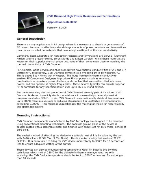
General Description:<br />
<strong>CVD</strong> <strong>Diamond</strong> <strong>High</strong> <strong>Power</strong> <strong>Resistors</strong> <strong>and</strong> Terminations<br />
Application Note 0022<br />
February 18, 2009<br />
There are many applications in RF design where it is necessary to absorb large amounts of<br />
RF power. In order to effectively absorb large amounts of power, resistors <strong>and</strong> terminations<br />
must be constructed on materials that have a high coefficient of thermal conductivity.<br />
Commonly used substrates for high power resistors <strong>and</strong> terminations are Beryllia, Aluminum<br />
Nitride, <strong>and</strong> to a lesser extent, Boron Nitride <strong>and</strong> Silicon Carbide. While these materials are<br />
known for their superior thermal properties, none of them come even close to matching the<br />
thermal conductivity of <strong>CVD</strong> <strong>Diamond</strong>.<br />
For example, while Beryllia <strong>and</strong> Aluminum Nitride have thermal conductivities of 2.5 <strong>and</strong> 1.7<br />
watts/cm/°C respectively, <strong>CVD</strong> <strong>Diamond</strong> comes in at a whopping 10 to 18 watts/cm/°C.<br />
This is about 3 to 4 times that of copper. This huge increase in thermal conductivity<br />
enables RF Component Designers to produce RF components such as resistors,<br />
terminations, attenuators, power dividers, <strong>and</strong> couplers that are smaller, dissipate more<br />
power, <strong>and</strong> can operate at higher frequencies. These devices typically can provide superior<br />
RF performance for any specified power level up to 26.5 GHz <strong>and</strong> beyond.<br />
But the outst<strong>and</strong>ing thermal properties of <strong>CVD</strong> <strong>Diamond</strong> are only part of it’s allure. <strong>CVD</strong><br />
<strong>Diamond</strong> is also an incredibly stable material since it is essentially chemically inert at<br />
temperatures below 300°C. In air, <strong>CVD</strong> <strong>Diamond</strong> is unconditionally stable at temperatures<br />
up to 600°C while in a vacuum or reducing atmosphere it is unaffected by temperatures<br />
exceeding 1,200°C . This makes it unquestionably the material of choice for high reliability<br />
<strong>and</strong> space applications.<br />
Mounting Instructions:<br />
<strong>CVD</strong> <strong>Diamond</strong> components manufactured by EMC Technology are designed to be mounted<br />
using conventional mounting techniques. The backside ground plane of the device is<br />
sputter coated with a solderable metal <strong>and</strong> finished with about 150 nm (5.9 micro-inches) of<br />
pure gold.<br />
The easiest method of attaching the device to a suitable heat sink is by soldering the unit<br />
with Sn96 solder (96.5% Tin / 3.5% Silver). This is a eutectic alloy that melts at 221°C<br />
(430°F). It is permissible to bring the <strong>CVD</strong> device momentarily to 300°C for 10 seconds or<br />
less to ensure adequate wetting of the surface.<br />
These devices can also be mounted using conventional Gold-Tin Eutectic Die Bonding<br />
techniques which melt at 280ºC for the ultimate in thermal management. As with<br />
soldering, the <strong>CVD</strong> Device temperature should be kept to 300ºC or less <strong>and</strong> for not longer<br />
than 10 seconds.
Dissipating the Heat:<br />
<strong>Resistors</strong> <strong>and</strong> Terminations manufactured on <strong>Diamond</strong> Substrates have the ability of<br />
dissipating huge amounts of thermal energy in spite of their extremely small size.<br />
Therefore, the heat sink should be constructed of a high thermal conductivity material such<br />
as copper <strong>and</strong> sized according to good thermal management practices. The physical size of<br />
the heat sink will be approximately the same as with any conventional device dissipating the<br />
same amount of thermal energy.<br />
Aluminum heat sinks can also be used, but it should be noted that the thermal conductivity<br />
of aluminum is approximately one-half that of copper. In situations where weight is a<br />
concern, an acceptable compromise would be to mount the <strong>CVD</strong> <strong>Diamond</strong> device on a<br />
copper heat spreader which in turn is attached to the aluminum heat sink.<br />
For particularly dem<strong>and</strong>ing applications, insulating or electrically conductive diamond heat<br />
spreaders are available to effectively transition the heat from the <strong>CVD</strong> device to an external<br />
chassis or bulkhead for further removal. <strong>Diamond</strong> heat spreaders are extremely small <strong>and</strong><br />
lightweight providing a highly efficient <strong>and</strong> convenient method of removing the heat from a<br />
circuit board to an external heat sink when space <strong>and</strong> weight is limited. Please contact the<br />
factory for additional details.<br />
Good Thermal Practices:<br />
Figure 1 shows the typical thermal path of a <strong>CVD</strong> device mounted on a copper heat sink.<br />
SOLDER<br />
THICKNESS<br />
THIN FILM<br />
RESISTOR<br />
ELEMENT<br />
COPPER<br />
HEAT SINK<br />
Figure 1<br />
ELECTRICAL<br />
CONTACTS<br />
<strong>CVD</strong> DIAMOND<br />
SUBSTRATE<br />
The thermal resistance across the attachment interface has a significant affect on the<br />
performance of the device. For instance, at 50 watts, the temperature differential across a<br />
Sn96 solder interface that is only 0.002 inches thick would be about 39°C for a device<br />
measuring 50 mils square. This is greater than the temperature differential across the<br />
entire <strong>CVD</strong> <strong>Diamond</strong> substrate at the same power level. Therefore, it is important to<br />
maintain the thickness of the solder to between 1 <strong>and</strong> 3 mils. For every 1 mil increase in<br />
the thickness of the solder, the temperature of the device will increase by approximately<br />
20°C therefore reducing it’s ability to absorb power.<br />
2
When soldering the <strong>CVD</strong> <strong>Diamond</strong> device to the heat sink, avoid introducing small pockets<br />
of air <strong>and</strong> flux, called solder voids, between the device <strong>and</strong> the heat sink. It is essential that<br />
solder voids be eliminated or at least reduced as much as possible in order to maximize the<br />
power h<strong>and</strong>ling capability of the device. Even small solder voids can substantially reduce<br />
the efficiency of the thermal interface resulting in devices that run considerably hotter than<br />
necessary.<br />
The thermal integrity of the soldered connection can easily be determined by measuring the<br />
temperature of the top surface of the device <strong>and</strong> comparing it with calculated data. For<br />
example, for a 50 mil square resistor running at 50 watts, the top surface of the device<br />
would normally measure about 60°C to 70°C higher than the heat sink temperature. If the<br />
device temperature is substantially higher than this, the solder interface should be<br />
considered suspect <strong>and</strong> be evaluated for voids or other discontinuities.<br />
Other silver-tin solder compositions such as Sn95 <strong>and</strong> Sn94 <strong>and</strong> many Lead-Free<br />
formulations can also be used with almost no degrading of performance. However, when<br />
using Tin-Lead solders such as Sn63 which have a melting temperature of 183°C, the<br />
maximum permissible input power or the heat sink temperature should be reduced to<br />
prevent the solder from melting. For example, a part rated at 50 watts on a 100°C heat<br />
sink should be derated by about 30% to 35 watts maximum when attached with Sn63<br />
solder.<br />
Epoxies can provide a very high-strength mechanical bond, however, they should be used<br />
with caution due to their generally poor thermal performance. When epoxies are used,<br />
consult with the manufacturer of the epoxy for the coefficient of thermal conductivity. If<br />
necessary, derate the maximum power rating of the <strong>CVD</strong> <strong>Diamond</strong> device accordingly.<br />
As a rule of thumb, the temperature differential across the attachment material should not<br />
exceed 40°C at the maximum rated power of the device. It can be calculated by the<br />
following expression:<br />
P × t<br />
Δ T =<br />
K × A<br />
where: ΔT = Temperature Differential in °C<br />
t = thickness of the interface in cm<br />
P = <strong>Power</strong> in watts<br />
A = Area in Square-cm<br />
K = Thermal Conductivity in Watts/cm/°C<br />
Typical values for the Coefficient of Thermal Conductivity of commonly used attachment<br />
materials are listed in the table below (Figure 2):<br />
3
Commonly Used Attachment Materials<br />
Material Composition<br />
Thermal<br />
Conductivity<br />
( Watts/cm/°C )<br />
Melting<br />
Temperature<br />
( °C )<br />
Gold-Tin Solder 80% Gold / 20% Tin 0.58 280<br />
Lead-Free Solder 99.3% Tin – 0.7% Copper N/A 227<br />
Lead-Free Solder 96.5% Tin / 3.5% Silver 0.33 221<br />
Lead-Free Solder 96.5% Tin / 3% Silver / 0.5% Copper N/A 217 - 220<br />
Sn63 Solder 63% Tin / 37% Lead 0.49 183<br />
Conductive Epoxy Silver Filled 0.01 to 0.29 N/A<br />
Flange Mounting:<br />
Figure 2<br />
A convenient way of mounting diamond resistors <strong>and</strong> terminations for good thermal<br />
performance is to first solder the devices to a copper flange, then screw the flange to a<br />
suitable heat sink. A small amount of thermal grease between the flange/heat-sink<br />
interface will assure a good thermal contact. This method of assembly eliminates the<br />
necessity of bringing the entire heat sink up to soldering temperature. Also, it allows the<br />
use of the existing external case or enclosure to be used as a heat dissipating surface<br />
instead of a dedicated heat sink, thereby saving space <strong>and</strong> weight.<br />
Shown below are typical views of diamond terminations mounted on gold plated copper<br />
flanges. Sn96 solder (96% Tin / 4% Silver) was used for attachment. (Liquidus at 221ºC)<br />
CT0505D & CT1310D Soldered to Gold Plated Copper Flange.<br />
4
Close-up View of CT0505D Soldered to Copper Flange<br />
The counterbore to the bottom-right of the device is for a thermocouple<br />
to measure flange temperature during power testing.<br />
Close-up View of CT1310D Soldered to Copper Flange<br />
5
Flip Chip Mounting:<br />
The preferential method of mounting diamond resistors <strong>and</strong> terminations is with the bottom<br />
of the chip securely attached to a suitable heat-sink of sufficient size to ensure maximum<br />
power dissipation. However, flip chip mounting can be considered when other<br />
considerations such as RF performance or capacitance to ground are of paramount<br />
importance. When using flip-chip mounting, most of the thermal energy will be dissipated<br />
by conduction through the electrical contacts. A small amount of the heat will also be<br />
dissipated from convection <strong>and</strong> radiation. Therefore, the maximum power rating of the<br />
device should be derated based on the physical geometry of the surrounding circuit.<br />
As an example, a CR0505D 50 Ohm resistor was attached to a microstrip line in a flip-chip<br />
configuration. The device was submitted to various power levels <strong>and</strong> the chip temperature<br />
was monitored. The graph in Figure 3 below shows the actual measured temperature on<br />
the exposed (top) side.<br />
Temperature (C)<br />
200<br />
175<br />
150<br />
125<br />
100<br />
75<br />
50<br />
25<br />
0<br />
Chip Temperature vs <strong>Power</strong><br />
0.0 0.5 1.0 1.5 2.0 2.5<br />
<strong>Power</strong> Applied (Watts)<br />
Figure 3<br />
NOTE: Operation above 150ºC is not recommended.<br />
6
Input Connections:<br />
The top side connections are finished with about 1 micron (39.4 micro-inches) of sputtered<br />
gold over a proprietary solderable metal. These electrical contacts are designed to be<br />
soldered or wire bonded to the external circuit.<br />
When wire bonding, conventional ultrasonic <strong>and</strong> thermo-compression wedge bonding<br />
techniques are recommended. The attachment wires can be either 1 mil diameter gold wire<br />
or 1x3 mil gold ribbon. Multiple wires should be used to reduce the input inductance <strong>and</strong> to<br />
increase the current capability of the connection.<br />
Tabs can also be attached to the input pads using commonly available solders such as those<br />
shown in Figure 2. Tab dimensions are typically between 10 mils <strong>and</strong> 63 mils wide <strong>and</strong> up<br />
to 0.5 inches long.<br />
RF Performance:<br />
Typical RF Performance for the CT1310D Termination<br />
For RF performance of other part numbers, please see Specification Control Document.<br />
7